JP6957801B2 - 回路基板 - Google Patents
回路基板 Download PDFInfo
- Publication number
- JP6957801B2 JP6957801B2 JP2016018930A JP2016018930A JP6957801B2 JP 6957801 B2 JP6957801 B2 JP 6957801B2 JP 2016018930 A JP2016018930 A JP 2016018930A JP 2016018930 A JP2016018930 A JP 2016018930A JP 6957801 B2 JP6957801 B2 JP 6957801B2
- Authority
- JP
- Japan
- Prior art keywords
- heat transfer
- transfer structure
- circuit board
- metal pattern
- electronic component
- Prior art date
- Legal status (The legal status is an assumption and is not a legal conclusion. Google has not performed a legal analysis and makes no representation as to the accuracy of the status listed.)
- Active
Links
Images
Classifications
-
- H—ELECTRICITY
- H05—ELECTRIC TECHNIQUES NOT OTHERWISE PROVIDED FOR
- H05K—PRINTED CIRCUITS; CASINGS OR CONSTRUCTIONAL DETAILS OF ELECTRIC APPARATUS; MANUFACTURE OF ASSEMBLAGES OF ELECTRICAL COMPONENTS
- H05K1/00—Printed circuits
- H05K1/02—Details
- H05K1/0201—Thermal arrangements, e.g. for cooling, heating or preventing overheating
- H05K1/0203—Cooling of mounted components
- H05K1/0204—Cooling of mounted components using means for thermal conduction connection in the thickness direction of the substrate
-
- H—ELECTRICITY
- H05—ELECTRIC TECHNIQUES NOT OTHERWISE PROVIDED FOR
- H05K—PRINTED CIRCUITS; CASINGS OR CONSTRUCTIONAL DETAILS OF ELECTRIC APPARATUS; MANUFACTURE OF ASSEMBLAGES OF ELECTRICAL COMPONENTS
- H05K3/00—Apparatus or processes for manufacturing printed circuits
- H05K3/46—Manufacturing multilayer circuits
- H05K3/4602—Manufacturing multilayer circuits characterized by a special circuit board as base or central core whereon additional circuit layers are built or additional circuit boards are laminated
- H05K3/4608—Manufacturing multilayer circuits characterized by a special circuit board as base or central core whereon additional circuit layers are built or additional circuit boards are laminated comprising an electrically conductive base or core
-
- H—ELECTRICITY
- H10—SEMICONDUCTOR DEVICES; ELECTRIC SOLID-STATE DEVICES NOT OTHERWISE PROVIDED FOR
- H10W—GENERIC PACKAGES, INTERCONNECTIONS, CONNECTORS OR OTHER CONSTRUCTIONAL DETAILS OF DEVICES COVERED BY CLASS H10
- H10W40/00—Arrangements for thermal protection or thermal control
- H10W40/20—Arrangements for cooling
- H10W40/22—Arrangements for cooling characterised by their shape, e.g. having conical or cylindrical projections
- H10W40/226—Arrangements for cooling characterised by their shape, e.g. having conical or cylindrical projections characterised by projecting parts, e.g. fins to increase surface area
- H10W40/228—Arrangements for cooling characterised by their shape, e.g. having conical or cylindrical projections characterised by projecting parts, e.g. fins to increase surface area the projecting parts being wire-shaped or pin-shaped
-
- H—ELECTRICITY
- H10—SEMICONDUCTOR DEVICES; ELECTRIC SOLID-STATE DEVICES NOT OTHERWISE PROVIDED FOR
- H10W—GENERIC PACKAGES, INTERCONNECTIONS, CONNECTORS OR OTHER CONSTRUCTIONAL DETAILS OF DEVICES COVERED BY CLASS H10
- H10W70/00—Package substrates; Interposers; Redistribution layers [RDL]
- H10W70/60—Insulating or insulated package substrates; Interposers; Redistribution layers
- H10W70/67—Insulating or insulated package substrates; Interposers; Redistribution layers characterised by their insulating layers or insulating parts
- H10W70/68—Shapes or dispositions thereof
- H10W70/685—Shapes or dispositions thereof comprising multiple insulating layers
-
- H—ELECTRICITY
- H05—ELECTRIC TECHNIQUES NOT OTHERWISE PROVIDED FOR
- H05K—PRINTED CIRCUITS; CASINGS OR CONSTRUCTIONAL DETAILS OF ELECTRIC APPARATUS; MANUFACTURE OF ASSEMBLAGES OF ELECTRICAL COMPONENTS
- H05K1/00—Printed circuits
- H05K1/02—Details
- H05K1/0201—Thermal arrangements, e.g. for cooling, heating or preventing overheating
- H05K1/0203—Cooling of mounted components
- H05K1/0207—Cooling of mounted components using internal conductor planes parallel to the surface for thermal conduction, e.g. power planes
-
- H—ELECTRICITY
- H05—ELECTRIC TECHNIQUES NOT OTHERWISE PROVIDED FOR
- H05K—PRINTED CIRCUITS; CASINGS OR CONSTRUCTIONAL DETAILS OF ELECTRIC APPARATUS; MANUFACTURE OF ASSEMBLAGES OF ELECTRICAL COMPONENTS
- H05K1/00—Printed circuits
- H05K1/02—Details
- H05K1/0213—Electrical arrangements not otherwise provided for
- H05K1/0216—Reduction of cross-talk, noise or electromagnetic interference
- H05K1/0218—Reduction of cross-talk, noise or electromagnetic interference by printed shielding conductors, ground planes or power plane
-
- H—ELECTRICITY
- H05—ELECTRIC TECHNIQUES NOT OTHERWISE PROVIDED FOR
- H05K—PRINTED CIRCUITS; CASINGS OR CONSTRUCTIONAL DETAILS OF ELECTRIC APPARATUS; MANUFACTURE OF ASSEMBLAGES OF ELECTRICAL COMPONENTS
- H05K1/00—Printed circuits
- H05K1/02—Details
- H05K1/0271—Arrangements for reducing stress or warp in rigid printed circuit boards, e.g. caused by loads, vibrations or differences in thermal expansion
-
- H—ELECTRICITY
- H05—ELECTRIC TECHNIQUES NOT OTHERWISE PROVIDED FOR
- H05K—PRINTED CIRCUITS; CASINGS OR CONSTRUCTIONAL DETAILS OF ELECTRIC APPARATUS; MANUFACTURE OF ASSEMBLAGES OF ELECTRICAL COMPONENTS
- H05K2201/00—Indexing scheme relating to printed circuits covered by H05K1/00
- H05K2201/03—Conductive materials
- H05K2201/032—Materials
- H05K2201/0323—Carbon
-
- H—ELECTRICITY
- H05—ELECTRIC TECHNIQUES NOT OTHERWISE PROVIDED FOR
- H05K—PRINTED CIRCUITS; CASINGS OR CONSTRUCTIONAL DETAILS OF ELECTRIC APPARATUS; MANUFACTURE OF ASSEMBLAGES OF ELECTRICAL COMPONENTS
- H05K2201/00—Indexing scheme relating to printed circuits covered by H05K1/00
- H05K2201/03—Conductive materials
- H05K2201/0332—Structure of the conductor
- H05K2201/0335—Layered conductors or foils
- H05K2201/0338—Layered conductor, e.g. layered metal substrate, layered finish layer or layered thin film adhesion layer
-
- H—ELECTRICITY
- H05—ELECTRIC TECHNIQUES NOT OTHERWISE PROVIDED FOR
- H05K—PRINTED CIRCUITS; CASINGS OR CONSTRUCTIONAL DETAILS OF ELECTRIC APPARATUS; MANUFACTURE OF ASSEMBLAGES OF ELECTRICAL COMPONENTS
- H05K2201/00—Indexing scheme relating to printed circuits covered by H05K1/00
- H05K2201/06—Thermal details
- H05K2201/066—Heatsink mounted on the surface of the printed circuit board [PCB]
-
- H—ELECTRICITY
- H05—ELECTRIC TECHNIQUES NOT OTHERWISE PROVIDED FOR
- H05K—PRINTED CIRCUITS; CASINGS OR CONSTRUCTIONAL DETAILS OF ELECTRIC APPARATUS; MANUFACTURE OF ASSEMBLAGES OF ELECTRICAL COMPONENTS
- H05K2201/00—Indexing scheme relating to printed circuits covered by H05K1/00
- H05K2201/10—Details of components or other objects attached to or integrated in a printed circuit board
- H05K2201/10227—Other objects, e.g. metallic pieces
- H05K2201/10416—Metallic blocks or heatsinks completely inserted in a PCB
-
- H—ELECTRICITY
- H10—SEMICONDUCTOR DEVICES; ELECTRIC SOLID-STATE DEVICES NOT OTHERWISE PROVIDED FOR
- H10W—GENERIC PACKAGES, INTERCONNECTIONS, CONNECTORS OR OTHER CONSTRUCTIONAL DETAILS OF DEVICES COVERED BY CLASS H10
- H10W90/00—Package configurations
- H10W90/701—Package configurations characterised by the relative positions of pads or connectors relative to package parts
-
- H—ELECTRICITY
- H10—SEMICONDUCTOR DEVICES; ELECTRIC SOLID-STATE DEVICES NOT OTHERWISE PROVIDED FOR
- H10W—GENERIC PACKAGES, INTERCONNECTIONS, CONNECTORS OR OTHER CONSTRUCTIONAL DETAILS OF DEVICES COVERED BY CLASS H10
- H10W90/00—Package configurations
- H10W90/701—Package configurations characterised by the relative positions of pads or connectors relative to package parts
- H10W90/721—Package configurations characterised by the relative positions of pads or connectors relative to package parts of bump connectors
- H10W90/724—Package configurations characterised by the relative positions of pads or connectors relative to package parts of bump connectors between a chip and a stacked insulating package substrate, interposer or RDL
Landscapes
- Engineering & Computer Science (AREA)
- Microelectronics & Electronic Packaging (AREA)
- Manufacturing & Machinery (AREA)
- Structure Of Printed Boards (AREA)
- Insulated Metal Substrates For Printed Circuits (AREA)
- Production Of Multi-Layered Print Wiring Board (AREA)
- Cooling Or The Like Of Semiconductors Or Solid State Devices (AREA)
Description
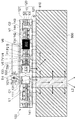
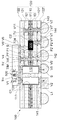
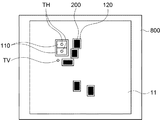
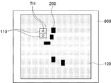
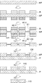
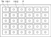
110 第1熱伝達用構造体
TH 機能孔
111 プライマー層
120 絶縁部
121 第1上部絶縁層
121' 第1下部絶縁層
122 第2上部絶縁層
122' 第2下部絶縁層
131 第1金属パターン
133 第3金属パターン
134 第7金属パターン
141 第2金属パターン
142 第4金属パターン
143 第5金属パターン
144 第6金属パターン
S ソルダ
200 第2電子部品
V1 第1ビア
V2 第2ビア
V4 第4ビア
V5 第5ビア
V6 第6ビア
V7 第7ビア
V8 第8 ビア
10 コア部
11 第1コア層
12 第2コア層
13 第3コア層
P1 第1回路パターン
P2 第2回路パターン
TV スルービア
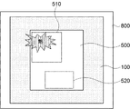
500 第1電子部品
800 付加基板
810 接続パッド
L1 第3熱伝達用構造体
L2 放熱部
C1 第1キャビティ
C2 第2キャビティ
Claims (11)
- 上面と下面とを含む柱形状を有し、熱伝導性物質で形成され、前記上面から前記下面まで貫通する機能孔が備えられた熱伝達用構造体が絶縁部に挿入され、
前記絶縁部には、さらに、コア層を含むコア部が備えられ、
前記熱伝達用構造体の表面には、前記熱伝達用構造体と前記絶縁部とが密着するように、プライマー層が備えられ、
前記プライマー層を貫通する第1ビア及び第2ビアが前記熱伝達用構造体の表面に接触し、
前記コア層はグラファイトを含み、前記熱伝達用構造体の側面と接触する、回路基板。 - 前記機能孔に絶縁物質が充填された請求項1に記載の回路基板。
- 前記機能孔に充填された絶縁物質は、前記絶縁部と一体になるように形成される請求項2に記載の回路基板。
- 前記熱伝達用構造体の上面に一面が接触する前記第1ビアと、
前記第1ビアの他面に接触する第1金属パターンと、
前記第1金属パターンに接続する第1結合部材と、をさらに含む請求項3に記載の回路基板。 - 前記第1結合部材は、第1電子部品に接続可能に設けられ、
前記第1電子部品は、第1領域と、動作の際に前記第1領域よりも温度が高くなる第2領域とを含む請求項4に記載の回路基板。 - 前記熱伝達用構造体の少なくとも一部が前記第1電子部品の垂直下方に位置するように形成される請求項5に記載の回路基板。
- 前記熱伝達用構造体の下面に一面が接触する前記第2ビアと、
前記第2ビアの他面に接触する第2金属パターンと、
前記第2金属パターンに接続する第2結合部材と、をさらに含み、
前記熱伝達用構造体の熱が前記第2ビア及び前記第2金属パターンを経由して前記第2結合部材に移動する請求項6に記載の回路基板。 - 複数の絶縁層と、前記複数の絶縁層に形成される複数の金属層と、前記複数の絶縁層のうちの少なくとも一つの絶縁層を貫通し、前記複数の金属層のうちの少なくとも二つの金属層を接続させる複数のビアと、を含み、
第1領域と、動作の際に前記第1領域よりも温度が高くなる第2領域とを含む第1電子部品に接続可能な複数のパッドが最外層の表面の金属層に形成された回路基板において、
キャビティが備えられ、コア層を含むコア部と、
前記キャビティに少なくとも一部が挿入され、熱伝導性物質で形成された熱伝達用構造体と、
前記熱伝達用構造体及び前記コア部を覆う絶縁層と、を含み、
前記コア層はグラファイトを含み、前記熱伝達用構造体の側面と接触し、
前記熱伝達用構造体は、上面と下面とを含む柱形状を有し、
前記上面から前記下面まで貫通する機能孔が備えられ、前記絶縁層を形成する物質が前記機能孔に充填され、
前記熱伝達用構造体の表面には、前記熱伝達用構造体と前記絶縁層とが密着するように、プライマー層が備えられ、
前記プライマー層を貫通する第1ビア及び第2ビアが形成された、回路基板。 - 前記熱伝達用構造体の上面に一面が接触する前記第1ビアと、
前記第1ビアの他面に接触する第1金属パターンと、
前記第1金属パターンに接続する第1結合部材と、をさらに含み、
前記第1結合部材は、前記第1電子部品に接続可能に設けられる請求項8に記載の回路基板。 - 前記熱伝達用構造体の下面に一面が接触する前記第2ビアと、
前記第2ビアの他面に接触する第2金属パターンと、
前記第2金属パターンに接続する第2結合部材と、をさらに含み、
前記第1電子部品の熱が前記第1結合部材、前記第1金属パターン、前記第1ビア、前記熱伝達用構造体、第2ビア及び前記第2金属パターンを経由して前記第2結合部材に移動する請求項9に記載の回路基板。 - 前記複数のパッドには熱が通過する第1パッド及び電気信号が通過する第2パッドが含まれ、前記第1結合部材は、前記第1パッドに接続可能に形成され、前記第2パッドに接続する導体は、前記熱伝達用構造体に接続しない請求項10に記載の回路基板。
Applications Claiming Priority (2)
| Application Number | Priority Date | Filing Date | Title |
|---|---|---|---|
| KR1020150049568A KR102411999B1 (ko) | 2015-04-08 | 2015-04-08 | 회로기판 |
| KR10-2015-0049568 | 2015-04-08 |
Publications (2)
| Publication Number | Publication Date |
|---|---|
| JP2016201532A JP2016201532A (ja) | 2016-12-01 |
| JP6957801B2 true JP6957801B2 (ja) | 2021-11-02 |
Family
ID=57112978
Family Applications (1)
| Application Number | Title | Priority Date | Filing Date |
|---|---|---|---|
| JP2016018930A Active JP6957801B2 (ja) | 2015-04-08 | 2016-02-03 | 回路基板 |
Country Status (3)
| Country | Link |
|---|---|
| US (1) | US9832856B2 (ja) |
| JP (1) | JP6957801B2 (ja) |
| KR (1) | KR102411999B1 (ja) |
Families Citing this family (10)
| Publication number | Priority date | Publication date | Assignee | Title |
|---|---|---|---|---|
| KR102295105B1 (ko) * | 2014-12-29 | 2021-08-31 | 삼성전기주식회사 | 회로기판 및 회로기판 제조방법 |
| TWI579987B (zh) * | 2015-12-22 | 2017-04-21 | 財團法人工業技術研究院 | 散熱模組 |
| JP6771308B2 (ja) * | 2016-05-02 | 2020-10-21 | 三菱電機株式会社 | 回路基板および半導体集積回路の実装構造 |
| KR102772158B1 (ko) * | 2019-02-12 | 2025-02-25 | 엘지이노텍 주식회사 | 회로기판 |
| JP2020174115A (ja) * | 2019-04-10 | 2020-10-22 | 株式会社フジクラ | 多層回路基板 |
| JP7439833B2 (ja) * | 2019-06-14 | 2024-02-28 | Tdk株式会社 | 電子部品内蔵基板及びこれを用いた回路モジュール |
| KR102802189B1 (ko) | 2020-05-04 | 2025-04-30 | 삼성전자주식회사 | 반도체 패키지 |
| JPWO2022004280A1 (ja) * | 2020-07-02 | 2022-01-06 | ||
| CN115708420A (zh) * | 2021-06-18 | 2023-02-21 | 华为技术有限公司 | 芯片封装结构及其制备方法、封装系统 |
| US11924962B2 (en) * | 2021-10-21 | 2024-03-05 | Dell Products L.P. | Printed circuit board (PCB) including heatsinks |
Family Cites Families (43)
| Publication number | Priority date | Publication date | Assignee | Title |
|---|---|---|---|---|
| US4396936A (en) * | 1980-12-29 | 1983-08-02 | Honeywell Information Systems, Inc. | Integrated circuit chip package with improved cooling means |
| JPH0423485A (ja) * | 1990-05-18 | 1992-01-27 | Cmk Corp | プリント配線板とその製造法 |
| US5200809A (en) * | 1991-09-27 | 1993-04-06 | Vlsi Technology, Inc. | Exposed die-attach heatsink package |
| DE69225896T2 (de) * | 1992-12-15 | 1998-10-15 | Sgs Thomson Microelectronics | Träger für Halbleitergehäuse |
| US6331731B1 (en) * | 1995-12-07 | 2001-12-18 | International Business Machines Corporation | Column for module component |
| US5831826A (en) * | 1996-09-20 | 1998-11-03 | Motorola, Inc. | Heat transfer apparatus suitable for use in a circuit board assembly |
| JP3684830B2 (ja) | 1998-03-27 | 2005-08-17 | イビデン株式会社 | プリント配線板 |
| US6430047B2 (en) | 1999-05-28 | 2002-08-06 | Agere Systems Guardian Corp. | Standardized test board for testing custom chips |
| JP4187352B2 (ja) | 1999-06-02 | 2008-11-26 | イビデン株式会社 | ビルドアップ多層プリント配線板及びビルドアップ多層プリント配線板の製造方法 |
| JP3573034B2 (ja) * | 1999-11-17 | 2004-10-06 | 日本電気株式会社 | 多層プリント配線板およびその放熱構造 |
| US6538210B2 (en) * | 1999-12-20 | 2003-03-25 | Matsushita Electric Industrial Co., Ltd. | Circuit component built-in module, radio device having the same, and method for producing the same |
| TW554069B (en) * | 2001-08-10 | 2003-09-21 | Ebara Corp | Plating device and method |
| DE10153763B4 (de) * | 2001-10-31 | 2006-09-28 | Advanced Micro Devices, Inc., Sunnyvale | Überwachung der Void-Bildung in einem Damascence-Prozess |
| US6873529B2 (en) * | 2002-02-26 | 2005-03-29 | Kyocera Corporation | High frequency module |
| JP3527229B2 (ja) * | 2002-05-20 | 2004-05-17 | 沖電気工業株式会社 | 半導体装置、半導体装置の実装方法、及び半導体装置のリペア方法 |
| JP4008782B2 (ja) * | 2002-08-23 | 2007-11-14 | 日本特殊陶業株式会社 | 多層配線基板の製造方法 |
| JP2005183559A (ja) * | 2003-12-18 | 2005-07-07 | Nec Corp | プリント配線板およびその製造方法 |
| JP4291729B2 (ja) * | 2004-04-23 | 2009-07-08 | 新光電気工業株式会社 | 基板及び半導体装置 |
| JP2006100631A (ja) * | 2004-09-30 | 2006-04-13 | Tdk Corp | 配線基板及びその製造方法 |
| JP4316483B2 (ja) * | 2004-12-08 | 2009-08-19 | ユーアイ電子株式会社 | プリント基板の製造方法及びプリント基板 |
| US7190581B1 (en) * | 2005-01-11 | 2007-03-13 | Midwest Research Institute | Low thermal resistance power module assembly |
| JP4697533B2 (ja) * | 2005-06-08 | 2011-06-08 | ミネベア株式会社 | 面状照明装置 |
| KR100691900B1 (ko) * | 2006-01-16 | 2007-03-09 | 삼성전자주식회사 | 하드디스크 드라이브 |
| US7629683B1 (en) * | 2006-02-28 | 2009-12-08 | Juniper Networks, Inc. | Thermal management of electronic devices |
| TW200806160A (en) * | 2006-07-07 | 2008-01-16 | Integrated Module Technology Inc | High heat conductive substrate and manufacturing method thereof |
| JP5142119B2 (ja) * | 2006-09-20 | 2013-02-13 | 住友電装株式会社 | 放熱構造を備えたプリント基板の製造方法および該方法で製造されたプリント基板の放熱構造 |
| JP2008140924A (ja) * | 2006-11-30 | 2008-06-19 | Toshiba Corp | 電子機器 |
| US7738249B2 (en) * | 2007-10-25 | 2010-06-15 | Endicott Interconnect Technologies, Inc. | Circuitized substrate with internal cooling structure and electrical assembly utilizing same |
| KR100976201B1 (ko) | 2007-10-30 | 2010-08-17 | 삼성전기주식회사 | 인쇄회로기판 및 그 제조 방법 |
| JP5026947B2 (ja) * | 2007-12-21 | 2012-09-19 | 矢崎総業株式会社 | 回路基板の熱対策構造 |
| JP2009200212A (ja) * | 2008-02-21 | 2009-09-03 | Keihin Corp | プリント基板の放熱構造 |
| US8166650B2 (en) | 2008-05-30 | 2012-05-01 | Steering Solutions IP Holding Company | Method of manufacturing a printed circuit board |
| US8248803B2 (en) * | 2010-03-31 | 2012-08-21 | Hong Kong Applied Science and Technology Research Institute Company Limited | Semiconductor package and method of manufacturing the same |
| JP2011222579A (ja) * | 2010-04-05 | 2011-11-04 | Kaneka Corp | 放熱構造体 |
| US8210716B2 (en) * | 2010-08-27 | 2012-07-03 | Quarkstar Llc | Solid state bidirectional light sheet for general illumination |
| JP2012253167A (ja) * | 2011-06-02 | 2012-12-20 | Denki Kagaku Kogyo Kk | 熱伝導性絶縁シート、金属ベース基板及び回路基板 |
| JP5987314B2 (ja) * | 2011-12-27 | 2016-09-07 | イビデン株式会社 | プリント配線板 |
| JP5692056B2 (ja) * | 2011-12-28 | 2015-04-01 | 株式会社デンソー | 多層プリント基板 |
| JP6119111B2 (ja) * | 2012-05-16 | 2017-04-26 | 富士通株式会社 | 回路基板、回路基板の製造方法、電子装置及び電子装置の製造方法 |
| JP2014192518A (ja) * | 2013-03-28 | 2014-10-06 | Toyota Motor Corp | 半導体装置およびその製造方法 |
| JP5764234B2 (ja) * | 2014-04-23 | 2015-08-19 | 島田理化工業株式会社 | プリント配線板の製造方法 |
| US9706668B2 (en) * | 2014-10-24 | 2017-07-11 | Samsung Electro-Mechanics Co., Ltd. | Printed circuit board, electronic module and method of manufacturing the same |
| KR102411997B1 (ko) * | 2015-04-08 | 2022-06-22 | 삼성전기주식회사 | 회로기판 및 회로기판 제조방법 |
-
2015
- 2015-04-08 KR KR1020150049568A patent/KR102411999B1/ko active Active
-
2016
- 2016-01-21 US US15/002,720 patent/US9832856B2/en active Active
- 2016-02-03 JP JP2016018930A patent/JP6957801B2/ja active Active
Also Published As
| Publication number | Publication date |
|---|---|
| US9832856B2 (en) | 2017-11-28 |
| KR20160120481A (ko) | 2016-10-18 |
| JP2016201532A (ja) | 2016-12-01 |
| US20160302298A1 (en) | 2016-10-13 |
| KR102411999B1 (ko) | 2022-06-22 |
Similar Documents
| Publication | Publication Date | Title |
|---|---|---|
| JP6957801B2 (ja) | 回路基板 | |
| KR102374256B1 (ko) | 회로기판 및 회로기판 제조방법 | |
| KR102262906B1 (ko) | 회로기판 | |
| JP6682741B2 (ja) | 回路基板及び回路基板組立体 | |
| JP6773366B2 (ja) | 回路基板及び回路基板の製造方法 | |
| JP5314889B2 (ja) | 電子装置及びその製造方法及び配線基板及びその製造方法 | |
| KR20160038293A (ko) | 회로기판 | |
| KR102253473B1 (ko) | 회로기판 | |
| US20190067543A1 (en) | Structure and manufacturing method of heat dissipation substrate and package structure and method thereof | |
| US9699885B2 (en) | Circuit board including heat dissipation structure | |
| US9345125B2 (en) | Wiring substrate | |
| CN206059386U (zh) | 布线基板以及电子装置 | |
| KR102149794B1 (ko) | 인쇄회로기판 및 그 제조방법 | |
| US8829361B2 (en) | Wiring board and mounting structure using the same | |
| CN1560911B (zh) | 电路载板的制造方法 | |
| KR101796519B1 (ko) | 회로기판 및 회로기판 조립체 | |
| JP7841678B2 (ja) | コンポーネントキャリア及びコンポーネントキャリアを製造する方法 | |
| TWI240368B (en) | Circuit carrier process |
Legal Events
| Date | Code | Title | Description |
|---|---|---|---|
| A621 | Written request for application examination |
Free format text: JAPANESE INTERMEDIATE CODE: A621 Effective date: 20190129 |
|
| A977 | Report on retrieval |
Free format text: JAPANESE INTERMEDIATE CODE: A971007 Effective date: 20200110 |
|
| A131 | Notification of reasons for refusal |
Free format text: JAPANESE INTERMEDIATE CODE: A131 Effective date: 20200121 |
|
| A521 | Request for written amendment filed |
Free format text: JAPANESE INTERMEDIATE CODE: A523 Effective date: 20200327 |
|
| A131 | Notification of reasons for refusal |
Free format text: JAPANESE INTERMEDIATE CODE: A131 Effective date: 20200526 |
|
| A521 | Request for written amendment filed |
Free format text: JAPANESE INTERMEDIATE CODE: A523 Effective date: 20200702 |
|
| A02 | Decision of refusal |
Free format text: JAPANESE INTERMEDIATE CODE: A02 Effective date: 20200929 |
|
| A521 | Request for written amendment filed |
Free format text: JAPANESE INTERMEDIATE CODE: A523 Effective date: 20210127 |
|
| C60 | Trial request (containing other claim documents, opposition documents) |
Free format text: JAPANESE INTERMEDIATE CODE: C60 Effective date: 20210127 |
|
| A911 | Transfer to examiner for re-examination before appeal (zenchi) |
Free format text: JAPANESE INTERMEDIATE CODE: A911 Effective date: 20210208 |
|
| C21 | Notice of transfer of a case for reconsideration by examiners before appeal proceedings |
Free format text: JAPANESE INTERMEDIATE CODE: C21 Effective date: 20210209 |
|
| A912 | Re-examination (zenchi) completed and case transferred to appeal board |
Free format text: JAPANESE INTERMEDIATE CODE: A912 Effective date: 20210409 |
|
| C211 | Notice of termination of reconsideration by examiners before appeal proceedings |
Free format text: JAPANESE INTERMEDIATE CODE: C211 Effective date: 20210413 |
|
| C22 | Notice of designation (change) of administrative judge |
Free format text: JAPANESE INTERMEDIATE CODE: C22 Effective date: 20210608 |
|
| C23 | Notice of termination of proceedings |
Free format text: JAPANESE INTERMEDIATE CODE: C23 Effective date: 20210803 |
|
| C03 | Trial/appeal decision taken |
Free format text: JAPANESE INTERMEDIATE CODE: C03 Effective date: 20210907 |
|
| C30A | Notification sent |
Free format text: JAPANESE INTERMEDIATE CODE: C3012 Effective date: 20210907 |
|
| A61 | First payment of annual fees (during grant procedure) |
Free format text: JAPANESE INTERMEDIATE CODE: A61 Effective date: 20210910 |
|
| R150 | Certificate of patent or registration of utility model |
Ref document number: 6957801 Country of ref document: JP Free format text: JAPANESE INTERMEDIATE CODE: R150 |
|
| R250 | Receipt of annual fees |
Free format text: JAPANESE INTERMEDIATE CODE: R250 |
|
| R250 | Receipt of annual fees |
Free format text: JAPANESE INTERMEDIATE CODE: R250 |