JP7045954B2 - ハードマスク用膜を形成する方法および装置、ならびに半導体装置の製造方法 - Google Patents
ハードマスク用膜を形成する方法および装置、ならびに半導体装置の製造方法 Download PDFInfo
- Publication number
- JP7045954B2 JP7045954B2 JP2018139051A JP2018139051A JP7045954B2 JP 7045954 B2 JP7045954 B2 JP 7045954B2 JP 2018139051 A JP2018139051 A JP 2018139051A JP 2018139051 A JP2018139051 A JP 2018139051A JP 7045954 B2 JP7045954 B2 JP 7045954B2
- Authority
- JP
- Japan
- Prior art keywords
- film
- hard mask
- forming
- microwave
- plasma
- Prior art date
- Legal status (The legal status is an assumption and is not a legal conclusion. Google has not performed a legal analysis and makes no representation as to the accuracy of the status listed.)
- Active
Links
Images


Classifications
-
- H—ELECTRICITY
- H01—ELECTRIC ELEMENTS
- H01J—ELECTRIC DISCHARGE TUBES OR DISCHARGE LAMPS
- H01J37/00—Discharge tubes with provision for introducing objects or material to be exposed to the discharge, e.g. for the purpose of examination or processing thereof
- H01J37/32—Gas-filled discharge tubes
- H01J37/32009—Arrangements for generation of plasma specially adapted for examination or treatment of objects, e.g. plasma sources
- H01J37/32192—Microwave generated discharge
- H01J37/32211—Means for coupling power to the plasma
- H01J37/3222—Antennas
-
- H—ELECTRICITY
- H10—SEMICONDUCTOR DEVICES; ELECTRIC SOLID-STATE DEVICES NOT OTHERWISE PROVIDED FOR
- H10P—GENERIC PROCESSES OR APPARATUS FOR THE MANUFACTURE OR TREATMENT OF DEVICES COVERED BY CLASS H10
- H10P76/00—Manufacture or treatment of masks on semiconductor bodies, e.g. by lithography or photolithography
- H10P76/40—Manufacture or treatment of masks on semiconductor bodies, e.g. by lithography or photolithography of masks comprising inorganic materials
- H10P76/408—Manufacture or treatment of masks on semiconductor bodies, e.g. by lithography or photolithography of masks comprising inorganic materials characterised by their sizes, orientations, dispositions, behaviours or shapes
- H10P76/4083—Manufacture or treatment of masks on semiconductor bodies, e.g. by lithography or photolithography of masks comprising inorganic materials characterised by their sizes, orientations, dispositions, behaviours or shapes characterised by their behaviours during the lithography processes, e.g. soluble masks or redeposited masks
-
- C—CHEMISTRY; METALLURGY
- C23—COATING METALLIC MATERIAL; COATING MATERIAL WITH METALLIC MATERIAL; CHEMICAL SURFACE TREATMENT; DIFFUSION TREATMENT OF METALLIC MATERIAL; COATING BY VACUUM EVAPORATION, BY SPUTTERING, BY ION IMPLANTATION OR BY CHEMICAL VAPOUR DEPOSITION, IN GENERAL; INHIBITING CORROSION OF METALLIC MATERIAL OR INCRUSTATION IN GENERAL
- C23C—COATING METALLIC MATERIAL; COATING MATERIAL WITH METALLIC MATERIAL; SURFACE TREATMENT OF METALLIC MATERIAL BY DIFFUSION INTO THE SURFACE, BY CHEMICAL CONVERSION OR SUBSTITUTION; COATING BY VACUUM EVAPORATION, BY SPUTTERING, BY ION IMPLANTATION OR BY CHEMICAL VAPOUR DEPOSITION, IN GENERAL
- C23C16/00—Chemical coating by decomposition of gaseous compounds, without leaving reaction products of surface material in the coating, i.e. chemical vapour deposition [CVD] processes
- C23C16/22—Chemical coating by decomposition of gaseous compounds, without leaving reaction products of surface material in the coating, i.e. chemical vapour deposition [CVD] processes characterised by the deposition of inorganic material, other than metallic material
- C23C16/30—Deposition of compounds, mixtures or solid solutions, e.g. borides, carbides, nitrides
- C23C16/34—Nitrides
- C23C16/345—Silicon nitride
-
- C—CHEMISTRY; METALLURGY
- C23—COATING METALLIC MATERIAL; COATING MATERIAL WITH METALLIC MATERIAL; CHEMICAL SURFACE TREATMENT; DIFFUSION TREATMENT OF METALLIC MATERIAL; COATING BY VACUUM EVAPORATION, BY SPUTTERING, BY ION IMPLANTATION OR BY CHEMICAL VAPOUR DEPOSITION, IN GENERAL; INHIBITING CORROSION OF METALLIC MATERIAL OR INCRUSTATION IN GENERAL
- C23C—COATING METALLIC MATERIAL; COATING MATERIAL WITH METALLIC MATERIAL; SURFACE TREATMENT OF METALLIC MATERIAL BY DIFFUSION INTO THE SURFACE, BY CHEMICAL CONVERSION OR SUBSTITUTION; COATING BY VACUUM EVAPORATION, BY SPUTTERING, BY ION IMPLANTATION OR BY CHEMICAL VAPOUR DEPOSITION, IN GENERAL
- C23C16/00—Chemical coating by decomposition of gaseous compounds, without leaving reaction products of surface material in the coating, i.e. chemical vapour deposition [CVD] processes
- C23C16/44—Chemical coating by decomposition of gaseous compounds, without leaving reaction products of surface material in the coating, i.e. chemical vapour deposition [CVD] processes characterised by the method of coating
- C23C16/455—Chemical coating by decomposition of gaseous compounds, without leaving reaction products of surface material in the coating, i.e. chemical vapour deposition [CVD] processes characterised by the method of coating characterised by the method used for introducing gases into reaction chamber or for modifying gas flows in reaction chamber
- C23C16/45523—Pulsed gas flow or change of composition over time
- C23C16/45525—Atomic layer deposition [ALD]
- C23C16/45527—Atomic layer deposition [ALD] characterized by the ALD cycle, e.g. different flows or temperatures during half-reactions, unusual pulsing sequence, use of precursor mixtures or auxiliary reactants or activations
- C23C16/45536—Use of plasma, radiation or electromagnetic fields
-
- C—CHEMISTRY; METALLURGY
- C23—COATING METALLIC MATERIAL; COATING MATERIAL WITH METALLIC MATERIAL; CHEMICAL SURFACE TREATMENT; DIFFUSION TREATMENT OF METALLIC MATERIAL; COATING BY VACUUM EVAPORATION, BY SPUTTERING, BY ION IMPLANTATION OR BY CHEMICAL VAPOUR DEPOSITION, IN GENERAL; INHIBITING CORROSION OF METALLIC MATERIAL OR INCRUSTATION IN GENERAL
- C23C—COATING METALLIC MATERIAL; COATING MATERIAL WITH METALLIC MATERIAL; SURFACE TREATMENT OF METALLIC MATERIAL BY DIFFUSION INTO THE SURFACE, BY CHEMICAL CONVERSION OR SUBSTITUTION; COATING BY VACUUM EVAPORATION, BY SPUTTERING, BY ION IMPLANTATION OR BY CHEMICAL VAPOUR DEPOSITION, IN GENERAL
- C23C16/00—Chemical coating by decomposition of gaseous compounds, without leaving reaction products of surface material in the coating, i.e. chemical vapour deposition [CVD] processes
- C23C16/44—Chemical coating by decomposition of gaseous compounds, without leaving reaction products of surface material in the coating, i.e. chemical vapour deposition [CVD] processes characterised by the method of coating
- C23C16/455—Chemical coating by decomposition of gaseous compounds, without leaving reaction products of surface material in the coating, i.e. chemical vapour deposition [CVD] processes characterised by the method of coating characterised by the method used for introducing gases into reaction chamber or for modifying gas flows in reaction chamber
- C23C16/45563—Gas nozzles
-
- C—CHEMISTRY; METALLURGY
- C23—COATING METALLIC MATERIAL; COATING MATERIAL WITH METALLIC MATERIAL; CHEMICAL SURFACE TREATMENT; DIFFUSION TREATMENT OF METALLIC MATERIAL; COATING BY VACUUM EVAPORATION, BY SPUTTERING, BY ION IMPLANTATION OR BY CHEMICAL VAPOUR DEPOSITION, IN GENERAL; INHIBITING CORROSION OF METALLIC MATERIAL OR INCRUSTATION IN GENERAL
- C23C—COATING METALLIC MATERIAL; COATING MATERIAL WITH METALLIC MATERIAL; SURFACE TREATMENT OF METALLIC MATERIAL BY DIFFUSION INTO THE SURFACE, BY CHEMICAL CONVERSION OR SUBSTITUTION; COATING BY VACUUM EVAPORATION, BY SPUTTERING, BY ION IMPLANTATION OR BY CHEMICAL VAPOUR DEPOSITION, IN GENERAL
- C23C16/00—Chemical coating by decomposition of gaseous compounds, without leaving reaction products of surface material in the coating, i.e. chemical vapour deposition [CVD] processes
- C23C16/44—Chemical coating by decomposition of gaseous compounds, without leaving reaction products of surface material in the coating, i.e. chemical vapour deposition [CVD] processes characterised by the method of coating
- C23C16/458—Chemical coating by decomposition of gaseous compounds, without leaving reaction products of surface material in the coating, i.e. chemical vapour deposition [CVD] processes characterised by the method of coating characterised by the method used for supporting substrates in the reaction chamber
- C23C16/4582—Rigid and flat substrates, e.g. plates or discs
- C23C16/4583—Rigid and flat substrates, e.g. plates or discs the substrate being supported substantially horizontally
-
- C—CHEMISTRY; METALLURGY
- C23—COATING METALLIC MATERIAL; COATING MATERIAL WITH METALLIC MATERIAL; CHEMICAL SURFACE TREATMENT; DIFFUSION TREATMENT OF METALLIC MATERIAL; COATING BY VACUUM EVAPORATION, BY SPUTTERING, BY ION IMPLANTATION OR BY CHEMICAL VAPOUR DEPOSITION, IN GENERAL; INHIBITING CORROSION OF METALLIC MATERIAL OR INCRUSTATION IN GENERAL
- C23C—COATING METALLIC MATERIAL; COATING MATERIAL WITH METALLIC MATERIAL; SURFACE TREATMENT OF METALLIC MATERIAL BY DIFFUSION INTO THE SURFACE, BY CHEMICAL CONVERSION OR SUBSTITUTION; COATING BY VACUUM EVAPORATION, BY SPUTTERING, BY ION IMPLANTATION OR BY CHEMICAL VAPOUR DEPOSITION, IN GENERAL
- C23C16/00—Chemical coating by decomposition of gaseous compounds, without leaving reaction products of surface material in the coating, i.e. chemical vapour deposition [CVD] processes
- C23C16/44—Chemical coating by decomposition of gaseous compounds, without leaving reaction products of surface material in the coating, i.e. chemical vapour deposition [CVD] processes characterised by the method of coating
- C23C16/46—Chemical coating by decomposition of gaseous compounds, without leaving reaction products of surface material in the coating, i.e. chemical vapour deposition [CVD] processes characterised by the method of coating characterised by the method used for heating the substrate
-
- C—CHEMISTRY; METALLURGY
- C23—COATING METALLIC MATERIAL; COATING MATERIAL WITH METALLIC MATERIAL; CHEMICAL SURFACE TREATMENT; DIFFUSION TREATMENT OF METALLIC MATERIAL; COATING BY VACUUM EVAPORATION, BY SPUTTERING, BY ION IMPLANTATION OR BY CHEMICAL VAPOUR DEPOSITION, IN GENERAL; INHIBITING CORROSION OF METALLIC MATERIAL OR INCRUSTATION IN GENERAL
- C23C—COATING METALLIC MATERIAL; COATING MATERIAL WITH METALLIC MATERIAL; SURFACE TREATMENT OF METALLIC MATERIAL BY DIFFUSION INTO THE SURFACE, BY CHEMICAL CONVERSION OR SUBSTITUTION; COATING BY VACUUM EVAPORATION, BY SPUTTERING, BY ION IMPLANTATION OR BY CHEMICAL VAPOUR DEPOSITION, IN GENERAL
- C23C16/00—Chemical coating by decomposition of gaseous compounds, without leaving reaction products of surface material in the coating, i.e. chemical vapour deposition [CVD] processes
- C23C16/44—Chemical coating by decomposition of gaseous compounds, without leaving reaction products of surface material in the coating, i.e. chemical vapour deposition [CVD] processes characterised by the method of coating
- C23C16/50—Chemical coating by decomposition of gaseous compounds, without leaving reaction products of surface material in the coating, i.e. chemical vapour deposition [CVD] processes characterised by the method of coating using electric discharges
- C23C16/511—Chemical coating by decomposition of gaseous compounds, without leaving reaction products of surface material in the coating, i.e. chemical vapour deposition [CVD] processes characterised by the method of coating using electric discharges using microwave discharges
-
- H—ELECTRICITY
- H01—ELECTRIC ELEMENTS
- H01J—ELECTRIC DISCHARGE TUBES OR DISCHARGE LAMPS
- H01J37/00—Discharge tubes with provision for introducing objects or material to be exposed to the discharge, e.g. for the purpose of examination or processing thereof
- H01J37/32—Gas-filled discharge tubes
- H01J37/32431—Constructional details of the reactor
- H01J37/32715—Workpiece holder
- H01J37/32724—Temperature
-
- H—ELECTRICITY
- H05—ELECTRIC TECHNIQUES NOT OTHERWISE PROVIDED FOR
- H05H—PLASMA TECHNIQUE; PRODUCTION OF ACCELERATED ELECTRICALLY-CHARGED PARTICLES OR OF NEUTRONS; PRODUCTION OR ACCELERATION OF NEUTRAL MOLECULAR OR ATOMIC BEAMS
- H05H1/00—Generating plasma; Handling plasma
- H05H1/24—Generating plasma
- H05H1/46—Generating plasma using applied electromagnetic fields, e.g. high frequency or microwave energy
-
- H—ELECTRICITY
- H10—SEMICONDUCTOR DEVICES; ELECTRIC SOLID-STATE DEVICES NOT OTHERWISE PROVIDED FOR
- H10P—GENERIC PROCESSES OR APPARATUS FOR THE MANUFACTURE OR TREATMENT OF DEVICES COVERED BY CLASS H10
- H10P14/00—Formation of materials, e.g. in the shape of layers or pillars
- H10P14/60—Formation of materials, e.g. in the shape of layers or pillars of insulating materials
- H10P14/63—Formation of materials, e.g. in the shape of layers or pillars of insulating materials characterised by the formation processes
- H10P14/6326—Deposition processes
- H10P14/6328—Deposition from the gas or vapour phase
- H10P14/6334—Deposition from the gas or vapour phase using decomposition or reaction of gaseous or vapour phase compounds, i.e. chemical vapour deposition
- H10P14/6336—Deposition from the gas or vapour phase using decomposition or reaction of gaseous or vapour phase compounds, i.e. chemical vapour deposition in the presence of a plasma [PECVD]
-
- H—ELECTRICITY
- H10—SEMICONDUCTOR DEVICES; ELECTRIC SOLID-STATE DEVICES NOT OTHERWISE PROVIDED FOR
- H10P—GENERIC PROCESSES OR APPARATUS FOR THE MANUFACTURE OR TREATMENT OF DEVICES COVERED BY CLASS H10
- H10P14/00—Formation of materials, e.g. in the shape of layers or pillars
- H10P14/60—Formation of materials, e.g. in the shape of layers or pillars of insulating materials
- H10P14/69—Inorganic materials
- H10P14/694—Inorganic materials composed of nitrides
- H10P14/6943—Inorganic materials composed of nitrides containing silicon
- H10P14/69433—Inorganic materials composed of nitrides containing silicon the material being a silicon nitride not containing oxygen, e.g. SixNy or SixByNz
-
- H—ELECTRICITY
- H10—SEMICONDUCTOR DEVICES; ELECTRIC SOLID-STATE DEVICES NOT OTHERWISE PROVIDED FOR
- H10P—GENERIC PROCESSES OR APPARATUS FOR THE MANUFACTURE OR TREATMENT OF DEVICES COVERED BY CLASS H10
- H10P50/00—Etching of wafers, substrates or parts of devices
- H10P50/20—Dry etching; Plasma etching; Reactive-ion etching
- H10P50/24—Dry etching; Plasma etching; Reactive-ion etching of semiconductor materials
- H10P50/242—Dry etching; Plasma etching; Reactive-ion etching of semiconductor materials of Group IV materials
-
- H—ELECTRICITY
- H10—SEMICONDUCTOR DEVICES; ELECTRIC SOLID-STATE DEVICES NOT OTHERWISE PROVIDED FOR
- H10P—GENERIC PROCESSES OR APPARATUS FOR THE MANUFACTURE OR TREATMENT OF DEVICES COVERED BY CLASS H10
- H10P50/00—Etching of wafers, substrates or parts of devices
- H10P50/20—Dry etching; Plasma etching; Reactive-ion etching
- H10P50/26—Dry etching; Plasma etching; Reactive-ion etching of conductive or resistive materials
- H10P50/264—Dry etching; Plasma etching; Reactive-ion etching of conductive or resistive materials by chemical means
- H10P50/266—Dry etching; Plasma etching; Reactive-ion etching of conductive or resistive materials by chemical means by vapour etching only
-
- H—ELECTRICITY
- H10—SEMICONDUCTOR DEVICES; ELECTRIC SOLID-STATE DEVICES NOT OTHERWISE PROVIDED FOR
- H10P—GENERIC PROCESSES OR APPARATUS FOR THE MANUFACTURE OR TREATMENT OF DEVICES COVERED BY CLASS H10
- H10P50/00—Etching of wafers, substrates or parts of devices
- H10P50/20—Dry etching; Plasma etching; Reactive-ion etching
- H10P50/28—Dry etching; Plasma etching; Reactive-ion etching of insulating materials
- H10P50/282—Dry etching; Plasma etching; Reactive-ion etching of insulating materials of inorganic materials
- H10P50/283—Dry etching; Plasma etching; Reactive-ion etching of insulating materials of inorganic materials by chemical means
-
- H—ELECTRICITY
- H10—SEMICONDUCTOR DEVICES; ELECTRIC SOLID-STATE DEVICES NOT OTHERWISE PROVIDED FOR
- H10P—GENERIC PROCESSES OR APPARATUS FOR THE MANUFACTURE OR TREATMENT OF DEVICES COVERED BY CLASS H10
- H10P50/00—Etching of wafers, substrates or parts of devices
- H10P50/71—Etching of wafers, substrates or parts of devices using masks for conductive or resistive materials
-
- H—ELECTRICITY
- H10—SEMICONDUCTOR DEVICES; ELECTRIC SOLID-STATE DEVICES NOT OTHERWISE PROVIDED FOR
- H10P—GENERIC PROCESSES OR APPARATUS FOR THE MANUFACTURE OR TREATMENT OF DEVICES COVERED BY CLASS H10
- H10P50/00—Etching of wafers, substrates or parts of devices
- H10P50/73—Etching of wafers, substrates or parts of devices using masks for insulating materials
-
- H—ELECTRICITY
- H10—SEMICONDUCTOR DEVICES; ELECTRIC SOLID-STATE DEVICES NOT OTHERWISE PROVIDED FOR
- H10P—GENERIC PROCESSES OR APPARATUS FOR THE MANUFACTURE OR TREATMENT OF DEVICES COVERED BY CLASS H10
- H10P72/00—Handling or holding of wafers, substrates or devices during manufacture or treatment thereof
- H10P72/04—Apparatus for manufacture or treatment
- H10P72/0402—Apparatus for fluid treatment
-
- H—ELECTRICITY
- H10—SEMICONDUCTOR DEVICES; ELECTRIC SOLID-STATE DEVICES NOT OTHERWISE PROVIDED FOR
- H10P—GENERIC PROCESSES OR APPARATUS FOR THE MANUFACTURE OR TREATMENT OF DEVICES COVERED BY CLASS H10
- H10P76/00—Manufacture or treatment of masks on semiconductor bodies, e.g. by lithography or photolithography
- H10P76/40—Manufacture or treatment of masks on semiconductor bodies, e.g. by lithography or photolithography of masks comprising inorganic materials
- H10P76/405—Manufacture or treatment of masks on semiconductor bodies, e.g. by lithography or photolithography of masks comprising inorganic materials characterised by their composition, e.g. multilayer masks
-
- H—ELECTRICITY
- H10—SEMICONDUCTOR DEVICES; ELECTRIC SOLID-STATE DEVICES NOT OTHERWISE PROVIDED FOR
- H10P—GENERIC PROCESSES OR APPARATUS FOR THE MANUFACTURE OR TREATMENT OF DEVICES COVERED BY CLASS H10
- H10P76/00—Manufacture or treatment of masks on semiconductor bodies, e.g. by lithography or photolithography
- H10P76/40—Manufacture or treatment of masks on semiconductor bodies, e.g. by lithography or photolithography of masks comprising inorganic materials
- H10P76/408—Manufacture or treatment of masks on semiconductor bodies, e.g. by lithography or photolithography of masks comprising inorganic materials characterised by their sizes, orientations, dispositions, behaviours or shapes
- H10P76/4085—Manufacture or treatment of masks on semiconductor bodies, e.g. by lithography or photolithography of masks comprising inorganic materials characterised by their sizes, orientations, dispositions, behaviours or shapes characterised by the processes involved to create the masks
-
- H—ELECTRICITY
- H01—ELECTRIC ELEMENTS
- H01J—ELECTRIC DISCHARGE TUBES OR DISCHARGE LAMPS
- H01J2237/00—Discharge tubes exposing object to beam, e.g. for analysis treatment, etching, imaging
- H01J2237/32—Processing objects by plasma generation
- H01J2237/33—Processing objects by plasma generation characterised by the type of processing
- H01J2237/332—Coating
- H01J2237/3321—CVD [Chemical Vapor Deposition]
-
- H—ELECTRICITY
- H10—SEMICONDUCTOR DEVICES; ELECTRIC SOLID-STATE DEVICES NOT OTHERWISE PROVIDED FOR
- H10P—GENERIC PROCESSES OR APPARATUS FOR THE MANUFACTURE OR TREATMENT OF DEVICES COVERED BY CLASS H10
- H10P72/00—Handling or holding of wafers, substrates or devices during manufacture or treatment thereof
- H10P72/04—Apparatus for manufacture or treatment
- H10P72/0431—Apparatus for thermal treatment
- H10P72/0432—Apparatus for thermal treatment mainly by conduction
-
- H—ELECTRICITY
- H10—SEMICONDUCTOR DEVICES; ELECTRIC SOLID-STATE DEVICES NOT OTHERWISE PROVIDED FOR
- H10P—GENERIC PROCESSES OR APPARATUS FOR THE MANUFACTURE OR TREATMENT OF DEVICES COVERED BY CLASS H10
- H10P72/00—Handling or holding of wafers, substrates or devices during manufacture or treatment thereof
- H10P72/06—Apparatus for monitoring, sorting, marking, testing or measuring
- H10P72/0602—Temperature monitoring
Landscapes
- Chemical & Material Sciences (AREA)
- Engineering & Computer Science (AREA)
- Physics & Mathematics (AREA)
- Plasma & Fusion (AREA)
- Organic Chemistry (AREA)
- General Chemical & Material Sciences (AREA)
- Chemical Kinetics & Catalysis (AREA)
- Materials Engineering (AREA)
- Mechanical Engineering (AREA)
- Metallurgy (AREA)
- Analytical Chemistry (AREA)
- Electromagnetism (AREA)
- Inorganic Chemistry (AREA)
- Spectroscopy & Molecular Physics (AREA)
- Chemical Vapour Deposition (AREA)
- Plasma Technology (AREA)
- Drying Of Semiconductors (AREA)
Description
最初に、実施形態のハードマスク膜の形成方法に至った経緯について説明する。
ハードマスクとしては、SiN膜等のシリコン系のものや、TiN膜のようなメタル系のものが多用されている。
次に、一実施形態に係るハードマスク用膜の形成方法について説明する。
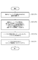
図5は一実施形態に係るハードマスク用膜の形成方法を示すフローチャート、図6A~6Bはその工程断面図である。
次に、以上のように形成されたハードマスク用膜4をハードマスクとして用いた半導体装置の製造方法について説明する。
図11は一実施形態に係る半導体装置の製造方法を示すフローチャート、図12はその工程断面図である。
次に、一実施形態に係るハードマスク用膜の形成に好適な成膜装置の例について説明する。本例の成膜装置は、小型のマイクロ波放射機構を複数有するマイクロ波プラズマ源を用いたマイクロ波プラズマ成膜装置として構成される。
以上、実施形態について説明したが、今回開示された実施形態は、全ての点で例示であって制限的なものではないと考えられるべきである。上記の実施形態は、添付の特許請求の範囲およびその主旨を逸脱することなく、様々な形態で省略、置換、変更されてもよい。
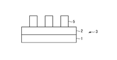
2;エッチング対象膜
3;基板
4;ハードマスク用膜
5;ハードマスク
6;残存部分
100;成膜装置
Claims (16)
- ハードマスク用膜を形成する方法であって、
基体上にエッチング対象膜が形成された基板を準備する工程と、
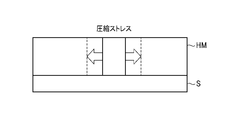
前記基板上に、ハードマスク用膜を、初期の膜ストレスが引張りストレスとなり、かつ引張りストレスが当該膜の底面から上面にかけて単調増加するように、成膜パラメータを制御しつつ成膜する工程と、
を有する、方法。 - 前記成膜する工程は、CVDにより行われる、請求項1に記載の方法。
- 前記成膜する工程は、プラズマCVDにより行われる、請求項2に記載の方法。
- 前記プラズマCVDを行う際のプラズマは、マイクロ波プラズマである、請求項3に記載の方法。
- 前記成膜パラメータは、成膜ガス流量、圧力、プラズマ密度の少なくとも1種である、請求項3または請求項4に記載の方法。
- 前記ハードマスク用膜は、SiN膜である、請求項1から請求項5のいずれか1項に記載の方法。
- 半導体装置の製造方法であって、
基体上にエッチング対象膜が形成された基板を準備する工程と、
前記基板上に、ハードマスク用膜を、初期の膜ストレスが引張りストレスとなり、かつ引張りストレスが当該膜の底面から上面にかけて単調増加するように、成膜パラメータを制御しつつ成膜する工程と、
前記ハードマスク用膜を所定パターンにエッチングし、ハードマスクを形成する工程と、
前記ハードマスクをマスクとして前記エッチング対象膜をエッチングする工程と、
を有する、方法。 - 前記成膜する工程は、CVDにより行われる、請求項7に記載の方法。
- 前記成膜する工程は、プラズマCVDにより行われる、請求項8に記載の方法。
- 前記プラズマCVDを行う際のプラズマは、マイクロ波プラズマである、請求項9に記載の方法。
- 前記成膜パラメータは、成膜速度、圧力、プラズマ密度の少なくとも1種である、請求項9または請求項10に記載の方法。
- 前記ハードマスク用膜は、SiN膜である、請求項7から請求項11のいずれか1項に記載の方法。
- ハードマスク用膜を成膜する装置であって、
基板を収容する処理容器と、
前記処理容器内で基板を載置する載置台と、
前記載置台上の被処理基板を加熱する加熱部と、
前記処理容器の天壁から前記処理容器内にマイクロ波を導入するマイクロ波導入部と、
前記処理容器内に成膜に用いる成膜ガスを供給するガス供給部と、
前記処理容器内を排気する排気部と、
制御部と、
を有し、
前記マイクロ波により成膜ガスのプラズマを生成し、該プラズマにより前記ハードマスク用膜を成膜し、
前記制御部は、ハードマスク用膜の初期の膜ストレスが引張りストレスとなり、かつ引張りストレスが当該膜の底面から上面にかけて単調増加するように、成膜パラメータを制御する、装置。 - 前記マイクロ波導入部は、
マイクロ波を出力するマイクロ波出力部と、
前記マイクロ波出力部からマイクロ波が給電され、インピーダンス整合を行うチューナと、給電されたマイクロ波を放射するスロットを有する平面アンテナと、前記スロットから放射されたマイクロ波を透過するマイクロ波透過板とを有する複数のマイクロ波放射機構と、
を有する、請求項13に記載の装置。 - 前記成膜パラメータは、成膜ガス流量、圧力、プラズマ密度の少なくとも1種である、請求項13または請求項14に記載の装置。
- 前記成膜ガスは、窒素含有ガスおよびSi原料ガスであり、ハードマスク用膜としてSiN膜を形成する、請求項13から請求項15のいずれか1項に記載の装置。
Priority Applications (3)
| Application Number | Priority Date | Filing Date | Title |
|---|---|---|---|
| JP2018139051A JP7045954B2 (ja) | 2018-07-25 | 2018-07-25 | ハードマスク用膜を形成する方法および装置、ならびに半導体装置の製造方法 |
| US16/510,519 US10879069B2 (en) | 2018-07-25 | 2019-07-12 | Method and apparatus for forming hard mask film and method for manufacturing semiconductor devices |
| KR1020190089311A KR102259647B1 (ko) | 2018-07-25 | 2019-07-24 | 하드 마스크용 막을 형성하는 방법 및 장치, 및 반도체 장치의 제조 방법 |
Applications Claiming Priority (1)
| Application Number | Priority Date | Filing Date | Title |
|---|---|---|---|
| JP2018139051A JP7045954B2 (ja) | 2018-07-25 | 2018-07-25 | ハードマスク用膜を形成する方法および装置、ならびに半導体装置の製造方法 |
Publications (2)
| Publication Number | Publication Date |
|---|---|
| JP2020017606A JP2020017606A (ja) | 2020-01-30 |
| JP7045954B2 true JP7045954B2 (ja) | 2022-04-01 |
Family
ID=69178595
Family Applications (1)
| Application Number | Title | Priority Date | Filing Date |
|---|---|---|---|
| JP2018139051A Active JP7045954B2 (ja) | 2018-07-25 | 2018-07-25 | ハードマスク用膜を形成する方法および装置、ならびに半導体装置の製造方法 |
Country Status (3)
| Country | Link |
|---|---|
| US (1) | US10879069B2 (ja) |
| JP (1) | JP7045954B2 (ja) |
| KR (1) | KR102259647B1 (ja) |
Families Citing this family (3)
| Publication number | Priority date | Publication date | Assignee | Title |
|---|---|---|---|---|
| KR102849886B1 (ko) * | 2021-01-20 | 2025-08-26 | 도쿄엘렉트론가부시키가이샤 | 기판 처리 방법 및 기판 처리 장치 |
| US11574808B2 (en) * | 2021-02-16 | 2023-02-07 | Tokyo Electron Limited | Plasma processing method and plasma processing apparatus |
| JP2024088507A (ja) * | 2022-12-20 | 2024-07-02 | 東京エレクトロン株式会社 | 基板処理方法及び基板処理装置 |
Citations (3)
| Publication number | Priority date | Publication date | Assignee | Title |
|---|---|---|---|---|
| US20080054415A1 (en) | 2006-08-31 | 2008-03-06 | Kai Frohberg | n-channel field effect transistor having a contact etch stop layer in combination with an interlayer dielectric sub-layer having the same type of intrinsic stress |
| JP2009246129A (ja) | 2008-03-31 | 2009-10-22 | Tokyo Electron Ltd | プラズマcvd窒化珪素膜の成膜方法及び半導体集積回路装置の製造方法 |
| JP2013543281A (ja) | 2010-11-22 | 2013-11-28 | アプライド マテリアルズ インコーポレイテッド | 複合的な除去可能ハードマスク |
Family Cites Families (8)
| Publication number | Priority date | Publication date | Assignee | Title |
|---|---|---|---|---|
| JP2993675B2 (ja) * | 1989-02-08 | 1999-12-20 | 株式会社日立製作所 | プラズマ処理方法及びその装置 |
| KR100557581B1 (ko) * | 2003-11-28 | 2006-03-03 | 주식회사 하이닉스반도체 | 반도체소자의 제조방법 |
| US7834399B2 (en) * | 2007-06-05 | 2010-11-16 | International Business Machines Corporation | Dual stress memorization technique for CMOS application |
| JP2009246131A (ja) | 2008-03-31 | 2009-10-22 | Tokyo Electron Ltd | 高ストレス薄膜の成膜方法及び半導体集積回路装置の製造方法 |
| JP2012015343A (ja) | 2010-07-01 | 2012-01-19 | Hitachi High-Technologies Corp | プラズマエッチング方法 |
| US9117668B2 (en) * | 2012-05-23 | 2015-08-25 | Novellus Systems, Inc. | PECVD deposition of smooth silicon films |
| JP6356029B2 (ja) | 2014-09-25 | 2018-07-11 | 東京エレクトロン株式会社 | メタルハードマスクおよびその製造方法 |
| JP6363266B2 (ja) | 2017-06-22 | 2018-07-25 | 株式会社日立ハイテクノロジーズ | 半導体装置の製造方法 |
-
2018
- 2018-07-25 JP JP2018139051A patent/JP7045954B2/ja active Active
-
2019
- 2019-07-12 US US16/510,519 patent/US10879069B2/en active Active
- 2019-07-24 KR KR1020190089311A patent/KR102259647B1/ko active Active
Patent Citations (3)
| Publication number | Priority date | Publication date | Assignee | Title |
|---|---|---|---|---|
| US20080054415A1 (en) | 2006-08-31 | 2008-03-06 | Kai Frohberg | n-channel field effect transistor having a contact etch stop layer in combination with an interlayer dielectric sub-layer having the same type of intrinsic stress |
| JP2009246129A (ja) | 2008-03-31 | 2009-10-22 | Tokyo Electron Ltd | プラズマcvd窒化珪素膜の成膜方法及び半導体集積回路装置の製造方法 |
| JP2013543281A (ja) | 2010-11-22 | 2013-11-28 | アプライド マテリアルズ インコーポレイテッド | 複合的な除去可能ハードマスク |
Also Published As
| Publication number | Publication date |
|---|---|
| US10879069B2 (en) | 2020-12-29 |
| JP2020017606A (ja) | 2020-01-30 |
| US20200035491A1 (en) | 2020-01-30 |
| KR102259647B1 (ko) | 2021-06-03 |
| KR20200011888A (ko) | 2020-02-04 |
Similar Documents
| Publication | Publication Date | Title |
|---|---|---|
| KR102751036B1 (ko) | 성막 방법 및 성막 장치 | |
| US12018375B2 (en) | Flim forming method of carbon-containing film by microwave plasma | |
| JP6752117B2 (ja) | マイクロ波プラズマ源およびマイクロ波プラズマ処理装置 | |
| JP2019055887A (ja) | グラフェン構造体の形成方法および形成装置 | |
| JP6700118B2 (ja) | プラズマ成膜装置および基板載置台 | |
| US20190237326A1 (en) | Selective film forming method and film forming apparatus | |
| US11972929B2 (en) | Processing apparatus and film forming method | |
| US12534800B2 (en) | Pre-coating method and processing apparatus | |
| KR101681061B1 (ko) | 플라즈마 처리 방법 및 플라즈마 처리 장치 | |
| JP7045954B2 (ja) | ハードマスク用膜を形成する方法および装置、ならびに半導体装置の製造方法 | |
| US10190217B2 (en) | Plasma film-forming method and plasma film-forming apparatus | |
| US12129544B2 (en) | Cleaning method and plasma treatment device | |
| WO2022102463A1 (ja) | 基板処理方法および基板処理装置 | |
| CN112652513A (zh) | 处理方法和等离子体处理装置 | |
| KR20250024998A (ko) | 기판 처리 방법 및 기판 처리 장치 | |
| JP2021192343A (ja) | プラズマ処理装置およびプラズマ処理方法 |
Legal Events
| Date | Code | Title | Description |
|---|---|---|---|
| A621 | Written request for application examination |
Free format text: JAPANESE INTERMEDIATE CODE: A621 Effective date: 20210426 |
|
| TRDD | Decision of grant or rejection written | ||
| A977 | Report on retrieval |
Free format text: JAPANESE INTERMEDIATE CODE: A971007 Effective date: 20220217 |
|
| A01 | Written decision to grant a patent or to grant a registration (utility model) |
Free format text: JAPANESE INTERMEDIATE CODE: A01 Effective date: 20220222 |
|
| A61 | First payment of annual fees (during grant procedure) |
Free format text: JAPANESE INTERMEDIATE CODE: A61 Effective date: 20220322 |
|
| R150 | Certificate of patent or registration of utility model |
Ref document number: 7045954 Country of ref document: JP Free format text: JAPANESE INTERMEDIATE CODE: R150 |
|
| R250 | Receipt of annual fees |
Free format text: JAPANESE INTERMEDIATE CODE: R250 |
|
| R250 | Receipt of annual fees |
Free format text: JAPANESE INTERMEDIATE CODE: R250 |