JP7082015B2 - Measuring device - Google Patents
Measuring device Download PDFInfo
- Publication number
- JP7082015B2 JP7082015B2 JP2018168935A JP2018168935A JP7082015B2 JP 7082015 B2 JP7082015 B2 JP 7082015B2 JP 2018168935 A JP2018168935 A JP 2018168935A JP 2018168935 A JP2018168935 A JP 2018168935A JP 7082015 B2 JP7082015 B2 JP 7082015B2
- Authority
- JP
- Japan
- Prior art keywords
- calibration
- measuring device
- output terminal
- current
- voltage
- Prior art date
- Legal status (The legal status is an assumption and is not a legal conclusion. Google has not performed a legal analysis and makes no representation as to the accuracy of the status listed.)
- Active
Links
Images


Classifications
-
- G—PHYSICS
- G01—MEASURING; TESTING
- G01N—INVESTIGATING OR ANALYSING MATERIALS BY DETERMINING THEIR CHEMICAL OR PHYSICAL PROPERTIES
- G01N15/00—Investigating characteristics of particles; Investigating permeability, pore-volume or surface-area of porous materials
- G01N15/10—Investigating individual particles
- G01N15/1031—Investigating individual particles by measuring electrical or magnetic effects
- G01N15/12—Investigating individual particles by measuring electrical or magnetic effects by observing changes in resistance or impedance across apertures when traversed by individual particles, e.g. by using the Coulter principle
- G01N15/131—Details
- G01N15/132—Circuits
Landscapes
- Chemical & Material Sciences (AREA)
- Biochemistry (AREA)
- Physics & Mathematics (AREA)
- Health & Medical Sciences (AREA)
- Life Sciences & Earth Sciences (AREA)
- Analytical Chemistry (AREA)
- Dispersion Chemistry (AREA)
- General Health & Medical Sciences (AREA)
- General Physics & Mathematics (AREA)
- Immunology (AREA)
- Pathology (AREA)
- Measurement Of Resistance Or Impedance (AREA)
- Amplifiers (AREA)
- Investigating Or Analyzing Materials By The Use Of Electric Means (AREA)
Description
本発明は、ナノポアデバイスを用いた計測に関する。 The present invention relates to measurement using a nanopore device.
電気的検知帯法(コールター原理)と呼ばれる粒度分布測定法が知られている。この測定法では、粒子を含む電界液を、ナノポアと称される細孔を通過させる。粒子が細孔を通過するとき、細孔中の電解液は粒子の体積に相当する量だけ減少し、細孔の電気抵抗を増加させる。したがって細孔の電気抵抗を測定することで、粒子より細孔の厚みの方が大きい場合には通過する粒子の体積を測定することができ、粒子より細孔の厚みの方が十分に小さい場合、通過している粒子の断面積(すなわち径)を測定することができる。 A particle size distribution measurement method called the electrical detection band method (Coulter principle) is known. In this measurement method, an electric field liquid containing particles is passed through pores called nanopores. As the particles pass through the pores, the electrolyte in the pores is reduced by an amount corresponding to the volume of the particles, increasing the electrical resistance of the pores. Therefore, by measuring the electrical resistance of the pores, the volume of the passing particles can be measured when the thickness of the pores is larger than that of the particles, and when the thickness of the pores is sufficiently smaller than that of the particles. , The cross-sectional area (ie, diameter) of the passing particles can be measured.
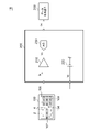
図1は、電気的検知帯法を用いた微粒子測定システム1Rのブロック図である。微粒子測定システム1Rは、ナノポアデバイス100、計測装置200Rおよびデータ処理装置300を備える。
FIG. 1 is a block diagram of a fine
ナノポアデバイス100の内部は、検出対象の粒子4を含む電解液2が満たされる。ナノポアデバイス100の内部は、ナノポアチップ102によって2つの空間に隔てられており、2つの空間には電極106と電極108が設けられる。電極106と電極108の間に電位差を発生させると、電極間にイオン電流が流れ、また電気泳動によって粒子4が細孔104を経由して、一方の空間から他方の空間に移動する。
The inside of the
計測装置200Rは、電極対106,108の間に電位差を発生させるとともに、電極対の間の抵抗値Rpと相関を有する情報を取得する。計測装置200Rは、トランスインピーダンスアンプ210、電圧源220、デジタイザ230を含む。電圧源220は電極対106,108の間に電位差Vbを発生させる。この電位差Vbは、電気泳動の駆動源であるとともに、抵抗値Rpを測定するためのバイアス信号となる。
The measuring device 200R generates a potential difference between the
電極対106,108の間には、細孔104の抵抗に反比例する微小電流Isが流れる。
Is=Vb/Rp …(1)
A minute current Is, which is inversely proportional to the resistance of the
Is = Vb / Rp ... (1)
トランスインピーダンスアンプ210は、微小電流Isを電圧信号Vsに変換する。変換ゲインをrとするとき、以下の式が成り立つ。
Vs=r×Is …(2)
式(1)を式(2)に代入すると、式(3)が得られる。
Vs=Vb×r/Rp …(3)
デジタイザ230は、電圧信号VsをデジタルデータDsに変換する。このように計測装置200Rにより、細孔104の抵抗値Rpに反比例する電圧信号Vsを得ることができる。
The
Vs = r × Is ... (2)
Substituting Eq. (1) into Eq. (2) gives Eq. (3).
Vs = Vb × r / Rp ... (3)
The
図2は、計測装置200Rにより測定される例示的な微小電流Isの波形図である。なお本明細書において参照する波形図やタイムチャートの縦軸および横軸は、理解を容易とするために適宜拡大、縮小したものであり、また示される各波形も、理解の容易のために簡略化され、あるいは誇張もしくは強調されている。 FIG. 2 is a waveform diagram of an exemplary minute current Is measured by the measuring device 200R. The vertical and horizontal axes of the waveform charts and time charts referred to in the present specification are appropriately enlarged or reduced for easy understanding, and each waveform shown is also simplified for easy understanding. It is made, or exaggerated or emphasized.
粒子が通過する短い期間、細孔104の抵抗値Rpが増大する。したがって、粒子が通過するごとに電流Isはパルス状に減少する。個々のパルス電流の振幅は、粒径と相関を有する。データ処理装置300は、デジタルデータDsを処理し、電解液2に含まれる粒子4の個数や粒径分布などを解析する。
The resistance value Rp of the
従来の微粒子測定システム1Rでは、粒径が既知(標準粒径という)である国際標準規格粒子を利用して測定(以下、校正測定と称する)を行い、その結果得られた信号強度(パルス電流の振幅)と標準粒径との対応関係を取得する。そして、任意の粒子を測定する際には、得られた信号強度と、校正測定で得られた相対関係にもとづいて、粒子の径を推定する。
In the conventional fine
従来の粒径の推定について詳しく説明する。図3は、国際標準規格粒子を測定したときに得られる信号強度のヒストグラムの一例である。横軸の信号強度は、パルス毎のデジタルデータDsの変化量、言い換えればパルス電流の振幅を示し、縦軸はパルスの個数を示す。 The conventional estimation of particle size will be described in detail. FIG. 3 is an example of a histogram of signal intensity obtained when measuring international standard particles. The signal strength on the horizontal axis indicates the amount of change in the digital data Ds for each pulse, in other words, the amplitude of the pulse current, and the vertical axis indicates the number of pulses.
図3のヒストグラムの中心は標準粒径φ0に対応する基準強度IREFとなる。したがって任意の粒子を測定したときに得られた信号強度がIxであったとき、その粒径φxは、IREFとR0の関係から推定される。 The center of the histogram in FIG. 3 is the reference intensity I REF corresponding to the standard particle size φ0 . Therefore, when the signal intensity obtained when measuring an arbitrary particle is I x , the particle size φ x is estimated from the relationship between I REF and R 0 .
このように従来の電気的検知帯法を利用した微粒子計測システム1Rでは、信号確度の電気的校正が実施されていない。したがって、デジタルデータDsが示すのは、電流量の相対値に過ぎず、デジタルデータDsに物理的な意味づけを与えることができない。そのため、測定器が入力信号に対して予期せぬ加工を加えている場合でも、その出力信号が正しいものと扱われてしまうおそれがある。
As described above, in the fine
この懸念から、従来では、微粒子測定システム1Rが生成する生データの一部のみを、粒径測定や粒子数計測に用いることができ、残りのデータは、無駄になっているといえる。裏を返すと、データの一部しか用いることができないため、粒子の形状の分析や、粒子がナノポアを通過する際の通過過渡現象の分析など、発展的なアプリケーションに応用することが難しい。なおこの問題を当業者の一般的な認識と捉えてはならない。
From this concern, it can be said that conventionally, only a part of the raw data generated by the fine
本発明は係る状況においてなされたものであり、そのある態様の例示的な目的のひとつは、電流や電圧の絶対値を測定可能な測定装置の提供にある。 The present invention has been made in such a situation, and one of the exemplary purposes of the embodiment is to provide a measuring device capable of measuring absolute values of current and voltage.
本発明のある態様は、細孔および電極対を有するナノポアデバイスのインピーダンスと相関を有する信号を測定する計測装置に関する。計測装置は、ナノポアデバイスの電極対と接続可能な出力端子対と、出力端子対の間のインピーダンスと相関を有するアナログ検出信号を生成するフロントエンド回路と、アナログ検出信号をデジタル検出信号に変換するA/Dコンバータと、を備える。出力端子対の間に、ナノポアデバイスに代えて既知の抵抗値を有する校正デバイスを接続可能であり、校正デバイスを接続した状態において、校正可能である。 One aspect of the invention relates to a measuring device that measures a signal that correlates with the impedance of a nanopore device having pores and electrode pairs. The measuring device has an output terminal pair that can be connected to the electrode pair of the nanopore device, a front-end circuit that generates an analog detection signal that correlates with the impedance between the output terminal pairs, and a front-end circuit that converts the analog detection signal into a digital detection signal. It is equipped with an A / D converter. A calibration device having a known resistance value can be connected between the output terminal pairs in place of the nanopore device, and calibration can be performed with the calibration device connected.
本発明の別の態様は、細孔および電極対を有するナノポアデバイスのインピーダンスと相関を有する信号を測定する計測装置の校正方法に関する。計測装置は、ナノポアデバイスの電極対と接続可能な出力端子対と、出力端子対の間に直流のバイアス電圧を印加可能なバイアス電圧源と、出力端子対の間に流れる電流信号を電圧信号に変換するトランスインピーダンスアンプと、トランスインピーダンスアンプの出力をデジタル値に変換するA/Dコンバータと、を備える。校正方法は、出力端子対の間に、ナノポアデバイスに代えて既知の抵抗を接続するステップと、既知の抵抗の間に、既知の直流バイアス電圧を印加し、そのときに得られるA/Dコンバータの出力を取得するステップと、A/Dコンバータの出力にもとづいて、校正用パラメータを取得するステップと、を備える。 Another aspect of the invention relates to a method of calibrating a measuring device that measures a signal that correlates with the impedance of a nanopore device having pores and electrode pairs. The measuring device uses an output terminal pair that can be connected to the electrode pair of the nanopore device, a bias voltage source that can apply a DC bias voltage between the output terminal pairs, and a current signal that flows between the output terminal pairs as a voltage signal. It includes a transimpedance amplifier for conversion and an A / D converter for converting the output of the transimpedance amplifier into a digital value. The calibration method is a step of connecting a known resistor instead of a nanopore device between the output terminal pairs, and an A / D converter obtained by applying a known DC bias voltage between the known resistors. It is provided with a step of acquiring the output of the above and a step of acquiring the calibration parameter based on the output of the A / D converter.
なお、以上の構成要素の任意の組み合わせや本発明の構成要素や表現を、方法、装置などの間で相互に置換したものもまた、本発明の態様として有効である。 It should be noted that any combination of the above components and the components and expressions of the present invention that are mutually replaced between methods, devices and the like are also effective as aspects of the present invention.
本発明のある態様によれば、電流信号や電圧信号の信号確度が保証された計測装置を提供できる。 According to an aspect of the present invention, it is possible to provide a measuring device in which the signal accuracy of a current signal or a voltage signal is guaranteed.
以下、本発明を好適な実施の形態をもとに図面を参照しながら説明する。各図面に示される同一または同等の構成要素、部材、処理には、同一の符号を付するものとし、適宜重複した説明は省略する。また、実施の形態は、発明を限定するものではなく例示であって、実施の形態に記述されるすべての特徴やその組み合わせは、必ずしも発明の本質的なものであるとは限らない。 Hereinafter, the present invention will be described with reference to the drawings based on the preferred embodiments. The same or equivalent components, members, and processes shown in the drawings shall be designated by the same reference numerals, and duplicate description thereof will be omitted as appropriate. Further, the embodiment is not limited to the invention, but is an example, and all the features and combinations thereof described in the embodiment are not necessarily essential to the invention.
本明細書において、「部材Aが、部材Bと接続された状態」とは、部材Aと部材Bが物理的に直接的に接続される場合のほか、部材Aと部材Bが、それらの電気的な接続状態に実質的な影響を及ぼさない、あるいはそれらの結合により奏される機能や効果を損なわせない、その他の部材を介して間接的に接続される場合も含む。 In the present specification, the "state in which the member A is connected to the member B" means that the member A and the member B are physically directly connected, and the member A and the member B are electrically connected to each other. It also includes cases of being indirectly connected via other members that do not substantially affect the connection state or impair the functions and effects performed by the combination thereof.
同様に、「部材Cが、部材Aと部材Bの間に設けられた状態」とは、部材Aと部材C、あるいは部材Bと部材Cが直接的に接続される場合のほか、それらの電気的な接続状態に実質的な影響を及ぼさない、あるいはそれらの結合により奏される機能や効果を損なわせない、その他の部材を介して間接的に接続される場合も含む。 Similarly, "a state in which the member C is provided between the member A and the member B" means that the member A and the member C, or the member B and the member C are directly connected, and their electricity. It also includes cases of being indirectly connected via other members that do not substantially affect the connection state or impair the functions and effects performed by the combination thereof.
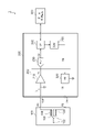
(基本構成)
図4は、実施の形態に係る微粒子測定システム1のブロック図である。微粒子測定システム1は、ナノポアデバイス100、計測装置200、データ処理装置300を備える。
(Basic configuration)
FIG. 4 is a block diagram of the fine particle measurement system 1 according to the embodiment. The fine particle measurement system 1 includes a
ナノポアデバイス100については、図1を参照して説明した通りであり、細孔104が設けられたナノポアチップ102と、電極対106,108を備える。ナノポアチップ102の内部は、KCl(塩化カリウム)やPBS(リン酸緩衝生理食塩水)などの電解液で満たされる。
The
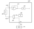
計測装置200は、出力端子対OUT1,OUT2、フロントエンド回路202、デジタイザ230、インタフェース240、キャリブレーションコントローラ250を備える。出力端子対OUT1,OUT2には、ナノポアデバイス100が着脱可能に接続される。ナノポアデバイス100が接続された状態において、出力端子対OUT1,OUTは、ナノポアデバイス100のピンP1,P2を介して、電極対106、108と電気的に接続される。フロントエンド回路202は、ナノポアデバイス100が装着された状態において、出力端子対OUT1,OUT2の間のインピーダンスと相関を有するアナログ検出信号Vsを生成可能である。
The measuring
デジタイザ230は、A/Dコンバータを含み、アナログ検出信号Vsをデジタル検出信号Dsに変換する。
The
本実施の形態においてフロントエンド回路202は、出力端子対OUT1,OUT2の間にバイアス電圧Vbを印加し、そのときに流れる電流Isを測定可能である。フロントエンド回路202は、トランスインピーダンスアンプ210および電圧源220を備える。
In the present embodiment, the front-
データ処理装置300は、ユーザとのインタフェースであり、また微粒子測定システム1を統合的に制御し、測定結果を取得、保存、表示する機能を備える。データ処理装置300は、汎用的なコンピュータやワークステーションであってもよいし、微粒子測定システム1専用に設計されたハードウェアであってもよい。
The
計測装置200は、通常測定モードと校正モードが切り替え可能である。データ処理装置300は、ユーザ(オペレータ)の操作に応じて、計測装置200の動作モードを切り替える。
The measuring
通常測定モードにおける動作は、図1の計測装置200Rと同様である。計測装置200の出力端子対OUT1,OUT2の間には、ナノポアデバイス100が接続される。電圧源220は、通常測定モードにおいて、電極対106,108の間に直流のバイアス電圧Vbを印加する。たとえば電圧源220はD/Aコンバータを含み、入力デジタルデータに応じたバイアス電圧Vbを発生する。トランスインピーダンスアンプ210は、ナノポアデバイス100に流れる電流Isを電圧信号Vsに変換する。デジタイザ230は電圧信号VsをデジタルデータDsに変換する。インタフェース240は、デジタルデータDsをデータ処理装置300に送信する。デジタルデータDsの時系列データは電流波形を表す。データ処理装置300は、通常測定モードで得られたデジタルデータDsを処理し、電解液2に含まれる粒子4の個数や粒径を取得する。さらには、以下で説明する校正モードにより電流信号や電圧信号の信号確度が保証されるため、電流波形にもとづいて粒子の形状をはじめとする詳細な特徴量の取得が可能となる。
The operation in the normal measurement mode is the same as that of the measuring device 200R of FIG. The
続いて校正モードについて説明する。インタフェース240がデータ処理装置300から所定の制御データを受信すると、計測装置200が電流校正モードにセットされる。キャリブレーションコントローラ250は、電流校正モードにおいて、計測装置200の動作を制御する。
Next, the calibration mode will be described. When the
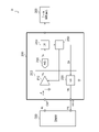
図5は、電流校正モードにおける微粒子測定システム1Cのブロック図である。電流校正モードにおいて、計測装置200の出力端子対OUT1,OUT2の間には、校正デバイス400が接続される。校正デバイス400は、既知の抵抗値を有する標準抵抗Rを含む。計測装置200は、校正デバイス400が接続された状態で、その内部の少なくとも一部分を校正可能となっている。
FIG. 5 is a block diagram of the fine
計測装置200は、デバイスホルダーを備えることができる。このデバイスホルダーには、ナノポアデバイス100が装着可能である。図4に示すように、ナノポアデバイス100は、電極対106,108と接続されるピンP1,P2を有する。デバイスホルダーからは、ナノポアデバイス100のピンP1,P2とコンタクト可能な態様で、出力端子対OUT1,OUT2が露出している。この場合において、校正デバイス400は、計測装置200のデバイスホルダーに装着可能であり、かつデバイスホルダーに装着した状態において出力端子対OUT1,OUT2とコンタクト可能なピンP1,P2を具備する。すなわち校正デバイス400とナノポアデバイス100は、形状やサイズにおいて互換性を有することが望ましい。これにより、ナノポアデバイス100を用いた粒子計測のときと、校正デバイス400を用いた校正のときとで、信号経路のインピーダンスなどを揃えることができ、キャリブレーションの精度を高めることができる。
The measuring
以上が微粒子測定システム1の構成である。続いてその動作を説明する。
1. 電流測定系の校正
はじめに、電流測定系、すなわちトランスインピーダンスアンプ210およびデジタイザ230の校正を説明する。この校正においては、電圧印加系、電圧源220は校正済みであり、バイアス電圧Vbの確度は保証されているものとする。電圧源220の校正については後述する。
The above is the configuration of the fine particle measurement system 1. Next, the operation will be described.
1. 1. Calibration of the current measurement system First, calibration of the current measurement system, that is, the
上述のように、電流校正モードでは計測装置200に、校正デバイス400が接続される。電流測定系の校正時に、データ処理装置300においてキャリブレーション用のプログラムが実行される。データ処理装置300は、計測装置200に制御データを送信し、計測装置200を電流校正モードにセットする。続いてデータ処理装置300は、バイアス電圧Vbの設定値Dbを、複数N個の値x1,x2,…,xNで切り替えながら、計測装置200に送信する。キャリブレーションコントローラ250は、データ処理装置300から受信した設定値xiを電圧源220に入力し、バイアス電圧Vbiを発生させる。
As described above, in the current calibration mode, the
フロントエンド回路202およびデジタイザ230は、バイアス電圧Vbi(i=1,2,…,N)に対応するデジタル検出信号Dsiを生成する。デジタル検出信号Dsi(i=1,2,…,N)は、データ処理装置300に送信される。
The front-
各バイアス電圧Vbに対して、デジタル検出信号Dsiを複数回、測定することが好ましい。この場合、複数回の測定で得られたデジタル検出信号Dsiの平均値miを計算する。 It is preferable to measure the digital detection signal Ds i a plurality of times for each bias voltage Vb. In this case, the average value mi of the digital detection signals Ds i obtained by a plurality of measurements is calculated.
図6(a)、(b)は、電流測定系の校正を説明する図である。図6(a)の横軸は印加したバイアス電圧Vbiを、縦軸は測定したデジタル検出信号の値miを表す。ここではN=2とする。データ処理装置300は、Vb=Vb1のときに得られた複数のデジタル検出信号Ds1の平均値m1を計算する。またデータ処理装置300は、Vb=Vb2のときに得られた複数のデジタル検出信号Ds2の平均値m2を計算する。
6 (a) and 6 (b) are diagrams illustrating calibration of the current measurement system. The horizontal axis of FIG. 6A represents the applied bias voltage Vbi , and the vertical axis represents the measured digital detection signal value mi . Here, N = 2. The
標準抵抗RにVbiを与えたときに流れる電流IiはIi=Vbi/Rである。この関係を用いて横軸を電流Iに書き換えたものが図6(b)に示される。 The current I i that flows when Vbi is applied to the standard resistance R is I i = Vb i / R. FIG. 6B shows a case in which the horizontal axis is rewritten to the current I using this relationship.
電流測定系の校正は、図6(b)において、測定値mと電流Iを関係づける関数を決定することと等価である。m1,m2,I1,I2が既知であるとき、任意のmに対応する電流Iは、以下の式(4)で表すことができる。
I=(I2-I1)/(m2-m1)×(m-m1)+I1 …(4)
Calibration of the current measurement system is equivalent to determining the function relating the measured value m and the current I in FIG. 6 (b). When m 1 , m 2 , I 1 , and I 2 are known, the current I corresponding to any m can be expressed by the following equation (4).
I = (I 2 -I 1 ) / (m 2 -m 1 ) x (m-m 1 ) + I 1 ... (4)
通常測定モードにおいて、ナノポアデバイス100を測定した結果、デジタル検出信号Dsの値としてmが得られたとき、それに対応する電流量の真値を、式(1)から計算することができる。
When m is obtained as the value of the digital detection signal Ds as a result of measuring the
この好ましくは、Vb1=0[V]とすると、校正処理を簡素化できる。
Vb1=0[V]のとき、I1=0[A]である。したがって、式(4)は式(5)に書き改めることができる。
I=I2/(m2-m1)×(m-m1) …(5)
I2=Vb2/Rを代入すると、式(6)を得る。
I=Vb2/{R×(m2-m1)}×(m-m1) …(6)
This preferably, when Vb 1 = 0 [V], the calibration process can be simplified.
When Vb 1 = 0 [V], I 1 = 0 [A]. Therefore, the equation (4) can be rewritten into the equation (5).
I = I 2 / (m 2 -m 1 ) x (m-m 1 ) ... (5)
Substituting I 2 = Vb 2 / R gives Eq. (6).
I = Vb 2 / {R × (m 2 -m 1 )} × (m-m 1 )… (6)
データ処理装置300は、測定値m1,m2を取得したのち、ゲインGAIN_CURを以下の式にもとづいて計算する。また測定値m1を、オフセットOFS_CURとして保持する。
GAIN_CUR=Vb2/{R×(m2-m1)}
OFS_CUR=m1
After acquiring the measured values m 1 and m 2 , the
GAIN_CUR = Vb 2 / {R × ( m2 - m1)}
OFS_CUR = m 1
そして通常測定時には、電流校正モードで取得したGAIN_CUR,OFS_CURにもとづいて、電流の真値を、式(7)にもとづいて計算することができる。
I=GAIN_CUR×(m-OFS_CUR) …(7)
Then, at the time of normal measurement, the true value of the current can be calculated based on the equation (7) based on the GAIN_CUR and OFS_CUR acquired in the current calibration mode.
I = GAIN_CUR × (m-OFS_CUR)… (7)
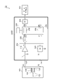
(電圧印加系の校正)
図7は、電圧校正モードにおける微粒子測定システム1Dのブロック図である。電圧印加系(電圧源220)を構成する際には、計測装置200の出力端子対OUT1,OUT2の間に、ナノポアデバイス100に代えて、デジタルマルチメータ500などの電圧測定器が接続される。
(Calibration of voltage application system)
FIG. 7 is a block diagram of the fine
電圧印加系の校正時に、データ処理装置300においてキャリブレーション用のプログラムが実行される。データ処理装置300は、計測装置200に制御データを送信し、計測装置200を電圧校正モードにセットする。続いてデータ処理装置300は、バイアス電圧Vbの設定値Dbを複数N個の値x1,x2,…,xNで切り替えながら、計測装置200に送信する。キャリブレーションコントローラ250は、データ処理装置300から受信した設定値xi(i=1,2,…,N)を電圧源220に入力し、バイアス電圧Vbiを発生させる。
At the time of calibration of the voltage application system, the calibration program is executed in the
デジタルマルチメータ500によって、バイアス電圧Vbi(i=1,2,…,N)が測定される。バイアス電圧Vbiの測定値biは、データ処理装置300に入力される。
The bias voltage Vbi ( i = 1, 2, ..., N) is measured by the
各バイアス電圧Vbに対して、デジタルマルチメータ500は、複数回の測定を行うことが好ましい。データ処理装置300は、バイアス電圧Vbiごとに、複数回の測定の平均値biを計算する。
For each bias voltage Vb, the
図8は、電圧印加系の校正を説明する図である。図8の横軸は、電圧源220に与える設定値Dbを、縦軸はデジタルマルチメータ500により測定したバイアス電圧Vbの値biを表す。ここではN=2とする。
FIG. 8 is a diagram illustrating calibration of the voltage application system. The horizontal axis of FIG. 8 represents the set value Db given to the
データ処理装置300は、設定値x1のときに得られたバイアス電圧Vb1の測定値b1を取得する。またデータ処理装置300は、設定値x2のときに得られたバイアス電圧Vb2の測定値b2を取得する。
The
図8の2点を通る関数g(x)は、式(8)で表される。
y=g(x)=(b2-b1)/(x2-x1)・(x-x1)+b1 …(8)
The function g (x) passing through the two points in FIG. 8 is represented by the equation (8).
y = g (x) = (b 2 -b 1 ) / (x 2 -x 1 ) · (x-x 1 ) + b 1 ... (8)
計測装置200において、任意のバイアス電圧Vbの値yを得るために必要な設定データDbの値x’は、式(9)で表される。
x’=g-1(y)=(x2-x1)/(b2-b1)・(y-b1)+x1 …(9)
In the
x'= g -1 (y) = (x 2 -x 1 ) / (b 2 -b 1 ) · (y-b 1 ) + x 1 ... (9)
データ処理装置300は、
GAIN_V=(x2-x1)/(b2-b1)
OFS_y=b1
OFS_x=x1
を計算し、それらの値を保持する。キャリブレーション完了後、通常の動作モードでは、任意のバイアス電圧yを生成する際には、Dsの値として、
x’=GAIN_V・(y-OFS_y)+OFS_x …(10)
を生成する。これにより正確なバイアス電圧Vbを生成することができる。
The
GAIN_V = (x 2 -x 1 ) / (b 2 -b 1 )
OFS_y = b 1
OFS_x = x 1
And keep their values. After the calibration is completed, in the normal operation mode, when generating an arbitrary bias voltage y, the value of Ds is set.
x'= GAIN_V ・ (y-OFS_y) + OFS_x ... (10)
To generate. This makes it possible to generate an accurate bias voltage Vb.
好ましくは、Vb1=0[V]とすると、校正処理を簡素化できる。このとき、x1=0であるから、計算すべきゲインとオフセットは、以下の式に修正される。
GAIN_V=x2/(b2-b1)
OFS_y=b1
OFS_x=0
となる。任意のバイアス電圧yを生成する際には、Dsの値として、
x’=GAIN_V・(y-OFS_y) …(11)
を生成すればよい。
Preferably, when Vb 1 = 0 [V], the calibration process can be simplified. At this time, since x 1 = 0, the gain and offset to be calculated are corrected by the following equations.
GAIN_V = x 2 / (b 2 -b 1 )
OFS_y = b 1
OFS_x = 0
Will be. When generating an arbitrary bias voltage y, as the value of Ds,
x'= GAIN_V ・ (y-OFS_y) ... (11)
Should be generated.
電流測定系の式(7)や、電圧印加系の式(11)に対応する演算は、計測装置200の内部で行ってもよい。図9は、計測装置200Dのブロック図である。
The calculation corresponding to the formula (7) of the current measurement system and the formula (11) of the voltage application system may be performed inside the measuring
上述の電圧校正モードにより、2つのパラメータGAIN_CUR、OFS_CURが生成される。これらのパラメータは、計測装置200のメモリ256に不揮発的に書き込まれる。
Two parameters GAIN_CUR and OFS_CUR are generated by the voltage calibration mode described above. These parameters are written non-volatilely to the
キャリブレーションコントローラ250Dは、第1演算部252を有する。第1演算部252は、通常動作モードにおいて、式(7)にしたがって、デジタルデータDsの値mを式(7)の電流値Iに変換する。インタフェース240は、変換後の正しい電流Iを示すデジタルデータDs’を、データ処理装置300に送信する。
The calibration controller 250D has a
また上述の電流校正モードにより、2つのパラメータGAIN_V、OFS_yが生成される。これらのパラメータも、計測装置200のメモリ256に不揮発的に書き込まれる。キャリブレーションコントローラ250Dは、第2演算部254を有する。第2演算部254は、通常動作モードにおいて、式(11)にしたがって、データ処理装置300から受信した設定データDsの値xを、式(11)の値x’に変換し、電圧源220に供給する。
Further, two parameters GAIN_V and OFS_y are generated by the above-mentioned current calibration mode. These parameters are also written non-volatilely to the
図10は、実施の形態に係る微粒子測定システム1における校正のフローチャートである。はじめに、電圧校正モード(S100)が実施され、電圧印加系を校正する。これにより、電圧源220が生成するバイアス電圧Vbの確度が保証される。
FIG. 10 is a flowchart of calibration in the fine particle measurement system 1 according to the embodiment. First, the voltage calibration mode (S100) is performed to calibrate the voltage application system. This guarantees the accuracy of the bias voltage Vb generated by the
続いて、電流校正モード(S102)が実施され、電流測定系を校正する。これにより、トランスインピーダンスアンプ210およデジタイザ230によって測定される電流信号の確度が保証される。これらの校正の完了後、通常の測定が可能となり、ナノポアデバイス100のインピーダンスが測定される。
Subsequently, the current calibration mode (S102) is executed to calibrate the current measurement system. This guarantees the accuracy of the current signal measured by the
そして、前回の校正実施から所定期間が経過するまで(S104のN)、通常測定時に、同じ校正パラメータが使用される。所定期間が経過すると(S104のY)、再び校正が行われる(S100,S102)。 Then, the same calibration parameter is used at the time of normal measurement until a predetermined period elapses from the previous calibration execution (N in S104). When the predetermined period elapses (Y in S104), calibration is performed again (S100, S102).
本実施の形態によれば、出力信号(デジタルデータDs)から求められる入力信号(電流信号Is)の値をある確度内に保証することができ、その絶対数値を、粒子の形状分析や過渡現象解析などの発展的アプリケーションに用いることができる。 According to this embodiment, the value of the input signal (current signal Is) obtained from the output signal (digital data Ds) can be guaranteed within a certain accuracy, and the absolute value can be used for particle shape analysis or transient phenomenon. It can be used for advanced applications such as analysis.
また出力信号値が入力信号にもとづくものであることが保証されるため、計測機器としての信頼性を担保できる。 Further, since the output signal value is guaranteed to be based on the input signal, the reliability as a measuring device can be guaranteed.
以上、本発明について、実施の形態をもとに説明した。この実施の形態は例示であり、それらの各構成要素や各処理プロセスの組み合わせにいろいろな変形例が可能なこと、またそうした変形例も本発明の範囲にあることは当業者に理解されるところである。以下、こうした変形例について説明する。 The present invention has been described above based on the embodiments. It is understood by those skilled in the art that this embodiment is an example, and that various modifications are possible for each of these components and combinations of each processing process, and that such modifications are also within the scope of the present invention. be. Hereinafter, such a modification will be described.
(変形例1)
校正で得られたパラメータは、データ処理装置300の内蔵メモリに不揮発的に保存しておき、計測装置200の起動のたびに、パラメータを計測装置200にロードするようにしてもよい。
(Modification 1)
The parameters obtained by the calibration may be stored non-volatilely in the built-in memory of the
(変形例2)
実施の形態では、データ処理装置300のプログラム制御により、校正を実現したがその限りでない。たとえばFPGA(Field Programmable Gate Array)やマイコン、ASIC(Application Specific Integrated)などのプロセッサを計測装置200に内蔵し、計測装置200に、校正用のプログラムを実行させてもよい。
(Modification 2)
In the embodiment, calibration is realized by the program control of the
(変形例3)
図11は、変形例3に係る計測装置200Eの電流測定系のブロック図である。図9では、計測装置200Dがデジタル信号処理によって、デジタルデータを補正した。図11では、計測装置200Eは、アナログ信号処理によって、デジタルデータを補正する。キャリブレーション用のハードウェア270は、加算器272、オフセット補正用のD/Aコンバータ274、ゲイン補正用のD/Aコンバータ276を含む。オフセット補正用のD/Aコンバータ274は、上述の電流校正モードで得られたオフセット補正値OFS_CURを、アナログのオフセット電圧VOFSに変換する。加算器272は、トランスインピーダンスアンプ210の出力電圧Vsに、オフセット電圧VOFSを加算する。ゲイン補正用のD/Aコンバータ276は、電流校正モードで得られたゲイン補正値GAIN_CURを、アナログの基準電圧VREFに変換し、デジタイザ230(A/Dコンバータ)の基準端子に供給する。
(Modification 3)
FIG. 11 is a block diagram of the current measuring system of the
(変形例4)
図12は、変形例4に係る計測装置200Fのブロック図である。計測装置200Fには、すでに校正済みの外部電圧源510を接続可能となっている。そして、出力端子OUT2から、内部の電圧源220の出力電圧VINTに変えて、外部電圧源510の出力電圧VEXTを、校正デバイス400に印加可能である。たとえば計測装置200Fは、外部電源接続ピン(EXT)と、マルチプレクサ(セレクタ)260を備えてもよい。電流校正モードにおいて、マルチプレクサ260は、外部電圧VEXTを選択することで、電圧印加系の校正完了前に、電流測定系の校正を行うことができる。
(Modification example 4)
FIG. 12 is a block diagram of the measuring
(変形例5)
図13は、変形例5に係る計測装置200Gのブロック図である。この変形例においてフロントエンド回路202Gは、出力端子対OUT1,OUT2の間に電流Ibを流し、そのときに出力端子対OUT1,OUT2の間に生ずる電圧Vsを測定可能である。フロントエンド回路202Gは、バイアス電流源280、アンプ282を含む。バイアス電流源280は、出力端子対OUT1,OUT2の間に直流のバイアス電流Ibを供給する。アンプ282は、出力端子対OUT1,OUT2の間に発生する電圧信号Vsを増幅し、デジタイザ230に供給する。
(Modification 5)
FIG. 13 is a block diagram of the measuring
計測装置200Gの校正は、アンプ282、デジタイザ230を含む電圧測定系と、バイアス電流源280を含む電流印加系に分けて実施することができる。電圧測定系の校正時には、出力端子対OUT1,OUT2に、標準抵抗を有する校正デバイス400を接続すればよい。また、電流印加系の校正時には、出力端子対OUT1,OUT2に、外部の電流測定装置を接続すればよい。校正処理自体は、上述したとおりである。
Calibration of the measuring
計測装置200Gは、外部電流源520が接続可能な接続端子(EXTピン)をさらに備えてもよい。校正時には、バイアス電流源280が生成するバイアス電流Ibに代えて、外部電流源520が生成する電流IEXTを、出力端子対に接続されるデバイスに供給可能である。計測装置200Gは、電流源を切り替えるためのセレクタ262を含んでもよい。
The measuring
(変形例6)
本明細書では微粒子計測装置について説明したが本発明の用途はそれに限定されず、DNAシーケンサをはじめとするナノポアデバイスを用いた微小電流計測を伴う計測器に広く用いることができる。
(Modification 6)
Although the fine particle measuring device has been described in the present specification, the application of the present invention is not limited to this, and it can be widely used for a measuring instrument accompanied by minute current measurement using a nanopore device such as a DNA sequencer.
実施の形態にもとづき本発明を説明したが、実施の形態は、本発明の原理、応用を示しているにすぎず、実施の形態には、請求の範囲に規定された本発明の思想を逸脱しない範囲において、多くの変形例や配置の変更が認められる。 Although the present invention has been described based on the embodiments, the embodiments merely show the principles and applications of the present invention, and the embodiments deviate from the ideas of the present invention defined in the claims. Many modifications and arrangement changes are allowed to the extent that they are not.
1 微粒子測定システム
2 電解液
4 粒子
100 ナノポアデバイス
102 ナノポアチップ
104 細孔
106,108 電極
110 シールドケース
200 計測装置
202 フロントエンド回路
210 トランスインピーダンスアンプ
220 電圧源
230 デジタイザ
240 インタフェース
250 キャリブレーションコントローラ
260 マルチプレクサ
270 バイアス電流源
272 アンプ
300 データ処理装置
400 校正デバイス
500 デジタルマルチメータ
510 外部電圧源
520 外部電流源
1 Fine
Claims (9)
ナノポアデバイスの電極対と接続可能な出力端子対を含み、測定時に、前記ナノポアデバイスが装着されるデバイスホルダーと、
前記出力端子対の間のインピーダンスと相関を有するアナログ検出信号を生成するフロントエンド回路と、
前記アナログ検出信号をデジタル検出信号に変換するA/Dコンバータと、
既知の抵抗値を有するとともに、ピン接続に関して前記ナノポアデバイスと互換性を有しており、校正時に、前記デバイスホルダーに装着される校正デバイスと、
を備え、
前記フロントエンド回路は、
前記出力端子対の間に直流のバイアス電圧を印加可能なバイアス電圧源と、
前記出力端子対の間に流れる電流信号を電圧信号に変換するトランスインピーダンスアンプと、
を含み、前記電圧信号が前記アナログ検出信号であり、
校正時に、前記校正デバイスを前記デバイスホルダーに装着した状態において、校正を実行することを特徴とする計測装置。 A measuring device that measures a signal that correlates with the impedance of a nanopore device that has pores and a pair of electrodes.
A device holder that includes an output terminal pair that can be connected to an electrode pair of a nanopore device and to which the nanopore device is mounted at the time of measurement.
A front-end circuit that generates an analog detection signal that correlates with the impedance between the output terminal pairs.
An A / D converter that converts the analog detection signal into a digital detection signal,
With a calibration device that has a known resistance value and is compatible with the nanopore device in terms of pin connection and is mounted on the device holder during calibration.
Equipped with
The front-end circuit
A bias voltage source to which a DC bias voltage can be applied between the output terminal pairs,
A transimpedance amplifier that converts the current signal flowing between the output terminal pairs into a voltage signal,
The voltage signal is the analog detection signal.
A measuring device characterized in that calibration is performed with the calibration device mounted on the device holder at the time of calibration.
校正時に、前記バイアス電圧源が生成するバイアス電圧に代えて、前記外部電圧源が生成する電圧を、前記出力端子対に印加可能であることを特徴とする請求項1から3のいずれかに記載の計測装置。 It also has a connection terminal to which an external voltage source can be connected.
The invention according to any one of claims 1 to 3 , wherein a voltage generated by the external voltage source can be applied to the output terminal pair in place of the bias voltage generated by the bias voltage source at the time of calibration. Measuring device.
校正時に、前記バイアス電流源が生成するバイアス電流に代えて、前記外部電流源が生成する電流を、前記出力端子対に供給可能であることを特徴とする請求項6から8のいずれかに記載の計測装置。 It also has a connection terminal to which an external current source can be connected.
6 . Measuring device.
Priority Applications (2)
| Application Number | Priority Date | Filing Date | Title |
|---|---|---|---|
| JP2018168935A JP7082015B2 (en) | 2018-09-10 | 2018-09-10 | Measuring device |
| DE102019123163.9A DE102019123163A1 (en) | 2018-09-10 | 2019-08-29 | MEASURING DEVICE AND CALIBRATION METHOD |
Applications Claiming Priority (1)
| Application Number | Priority Date | Filing Date | Title |
|---|---|---|---|
| JP2018168935A JP7082015B2 (en) | 2018-09-10 | 2018-09-10 | Measuring device |
Publications (2)
| Publication Number | Publication Date |
|---|---|
| JP2020041894A JP2020041894A (en) | 2020-03-19 |
| JP7082015B2 true JP7082015B2 (en) | 2022-06-07 |
Family
ID=69621229
Family Applications (1)
| Application Number | Title | Priority Date | Filing Date |
|---|---|---|---|
| JP2018168935A Active JP7082015B2 (en) | 2018-09-10 | 2018-09-10 | Measuring device |
Country Status (2)
| Country | Link |
|---|---|
| JP (1) | JP7082015B2 (en) |
| DE (1) | DE102019123163A1 (en) |
Families Citing this family (1)
| Publication number | Priority date | Publication date | Assignee | Title |
|---|---|---|---|---|
| CN113740397B (en) * | 2020-05-27 | 2024-05-28 | 成都今是科技有限公司 | Microcurrent detection circuit and gene sequencing device |
Citations (5)
| Publication number | Priority date | Publication date | Assignee | Title |
|---|---|---|---|---|
| JP2009128057A (en) | 2007-11-20 | 2009-06-11 | Sekisui Chem Co Ltd | Fine particle counter and fine particle counter chip |
| US20110285409A1 (en) | 2009-01-31 | 2011-11-24 | Teimour Maleki | Nanofluidic channel with embedded transverse nanoelectrodes and method of fabricating for same |
| JP2016102749A (en) | 2014-11-28 | 2016-06-02 | 株式会社アドバンテスト | measuring device |
| JP2016102748A (en) | 2014-11-28 | 2016-06-02 | 株式会社アドバンテスト | Current measuring device and base sequence analyzer; and measurement chip |
| JP2018112566A (en) | 2018-04-26 | 2018-07-19 | 株式会社アドバンテスト | Measuring apparatus |
Family Cites Families (1)
| Publication number | Priority date | Publication date | Assignee | Title |
|---|---|---|---|---|
| JP3851375B2 (en) * | 1996-04-18 | 2006-11-29 | アジレント・テクノロジーズ・インク | Impedance measuring device |
-
2018
- 2018-09-10 JP JP2018168935A patent/JP7082015B2/en active Active
-
2019
- 2019-08-29 DE DE102019123163.9A patent/DE102019123163A1/en active Pending
Patent Citations (5)
| Publication number | Priority date | Publication date | Assignee | Title |
|---|---|---|---|---|
| JP2009128057A (en) | 2007-11-20 | 2009-06-11 | Sekisui Chem Co Ltd | Fine particle counter and fine particle counter chip |
| US20110285409A1 (en) | 2009-01-31 | 2011-11-24 | Teimour Maleki | Nanofluidic channel with embedded transverse nanoelectrodes and method of fabricating for same |
| JP2016102749A (en) | 2014-11-28 | 2016-06-02 | 株式会社アドバンテスト | measuring device |
| JP2016102748A (en) | 2014-11-28 | 2016-06-02 | 株式会社アドバンテスト | Current measuring device and base sequence analyzer; and measurement chip |
| JP2018112566A (en) | 2018-04-26 | 2018-07-19 | 株式会社アドバンテスト | Measuring apparatus |
Also Published As
| Publication number | Publication date |
|---|---|
| JP2020041894A (en) | 2020-03-19 |
| DE102019123163A1 (en) | 2020-03-12 |
Similar Documents
| Publication | Publication Date | Title |
|---|---|---|
| JP3907353B2 (en) | Bioimpedance measurement device | |
| CN113614555B (en) | Impedance Standard | |
| JP2003219565A (en) | Calibration method and calibration device for battery charge / discharge system | |
| CN109073683B (en) | Method and battery sensor for determining load current | |
| CN113138341A (en) | Measuring device and measuring method for electricity storage device | |
| JP7082015B2 (en) | Measuring device | |
| JP5641627B2 (en) | Subsystem and method for use in a patch clamp system | |
| WO2021192578A1 (en) | Fine particle measuring system, and measurement device | |
| KR101968375B1 (en) | Method for Controlling Electrodes for Bio-impedance Measurements and Apparatus for Bio-impedance Measurements | |
| CN110646494B (en) | Circuit arrangement and corresponding method for operating an electrochemical cell | |
| CN120760893A (en) | Neutral electrode thermal effect testing method and system | |
| CN218767949U (en) | Voltage output circuit and voltage output device | |
| EP4306948A1 (en) | Validation of electrochemical measurements using a potentiostat | |
| JP2007064834A (en) | Device characteristic measurement system | |
| JP4744025B2 (en) | Method for determining connection state of gas sensor and constant potential electrolytic gas measuring instrument | |
| JP7802999B1 (en) | Calibration device and calibration method for charge/discharge testing device | |
| KR100834542B1 (en) | Vein measuring device | |
| JP2016085087A (en) | Method for determining wiring cable length in circuit element measurement device | |
| RU2121336C1 (en) | Method of measuring of electrodermal resistance | |
| US8346496B1 (en) | Apparatus and method for multi-channel materials assaying | |
| SU382092A1 (en) | 8THE UNION I | |
| JPS6313486Y2 (en) | ||
| JP5641626B6 (en) | Subsystem and method for use in a patch clamp system | |
| KR20250095935A (en) | Circuit and method for determining the sensitivity of a bridge circuit | |
| CN121955518A (en) | Resistance measuring circuit and resistance measuring device |
Legal Events
| Date | Code | Title | Description |
|---|---|---|---|
| A621 | Written request for application examination |
Free format text: JAPANESE INTERMEDIATE CODE: A621 Effective date: 20210513 |
|
| A977 | Report on retrieval |
Free format text: JAPANESE INTERMEDIATE CODE: A971007 Effective date: 20220217 |
|
| A131 | Notification of reasons for refusal |
Free format text: JAPANESE INTERMEDIATE CODE: A131 Effective date: 20220301 |
|
| A521 | Request for written amendment filed |
Free format text: JAPANESE INTERMEDIATE CODE: A523 Effective date: 20220428 |
|
| TRDD | Decision of grant or rejection written | ||
| A01 | Written decision to grant a patent or to grant a registration (utility model) |
Free format text: JAPANESE INTERMEDIATE CODE: A01 Effective date: 20220524 |
|
| A61 | First payment of annual fees (during grant procedure) |
Free format text: JAPANESE INTERMEDIATE CODE: A61 Effective date: 20220526 |
|
| R150 | Certificate of patent or registration of utility model |
Ref document number: 7082015 Country of ref document: JP Free format text: JAPANESE INTERMEDIATE CODE: R150 |
|
| R250 | Receipt of annual fees |
Free format text: JAPANESE INTERMEDIATE CODE: R250 |