JP7100577B2 - 表示装置および電子機器 - Google Patents
表示装置および電子機器 Download PDFInfo
- Publication number
- JP7100577B2 JP7100577B2 JP2018513064A JP2018513064A JP7100577B2 JP 7100577 B2 JP7100577 B2 JP 7100577B2 JP 2018513064 A JP2018513064 A JP 2018513064A JP 2018513064 A JP2018513064 A JP 2018513064A JP 7100577 B2 JP7100577 B2 JP 7100577B2
- Authority
- JP
- Japan
- Prior art keywords
- transistor
- video signal
- display device
- drive transistor
- signal writing
- Prior art date
- Legal status (The legal status is an assumption and is not a legal conclusion. Google has not performed a legal analysis and makes no representation as to the accuracy of the status listed.)
- Active
Links
Images


Classifications
-
- G—PHYSICS
- G09—EDUCATION; CRYPTOGRAPHY; DISPLAY; ADVERTISING; SEALS
- G09G—ARRANGEMENTS OR CIRCUITS FOR CONTROL OF INDICATING DEVICES USING STATIC MEANS TO PRESENT VARIABLE INFORMATION
- G09G3/00—Control arrangements or circuits, of interest only in connection with visual indicators other than cathode-ray tubes
- G09G3/20—Control arrangements or circuits, of interest only in connection with visual indicators other than cathode-ray tubes for presentation of an assembly of a number of characters, e.g. a page, by composing the assembly by combination of individual elements arranged in a matrix no fixed position being assigned to or needed to be assigned to the individual characters or partial characters
- G09G3/22—Control arrangements or circuits, of interest only in connection with visual indicators other than cathode-ray tubes for presentation of an assembly of a number of characters, e.g. a page, by composing the assembly by combination of individual elements arranged in a matrix no fixed position being assigned to or needed to be assigned to the individual characters or partial characters using controlled light sources
- G09G3/30—Control arrangements or circuits, of interest only in connection with visual indicators other than cathode-ray tubes for presentation of an assembly of a number of characters, e.g. a page, by composing the assembly by combination of individual elements arranged in a matrix no fixed position being assigned to or needed to be assigned to the individual characters or partial characters using controlled light sources using electroluminescent panels
- G09G3/32—Control arrangements or circuits, of interest only in connection with visual indicators other than cathode-ray tubes for presentation of an assembly of a number of characters, e.g. a page, by composing the assembly by combination of individual elements arranged in a matrix no fixed position being assigned to or needed to be assigned to the individual characters or partial characters using controlled light sources using electroluminescent panels semiconductive, e.g. using light-emitting diodes [LED]
- G09G3/3208—Control arrangements or circuits, of interest only in connection with visual indicators other than cathode-ray tubes for presentation of an assembly of a number of characters, e.g. a page, by composing the assembly by combination of individual elements arranged in a matrix no fixed position being assigned to or needed to be assigned to the individual characters or partial characters using controlled light sources using electroluminescent panels semiconductive, e.g. using light-emitting diodes [LED] organic, e.g. using organic light-emitting diodes [OLED]
- G09G3/3225—Control arrangements or circuits, of interest only in connection with visual indicators other than cathode-ray tubes for presentation of an assembly of a number of characters, e.g. a page, by composing the assembly by combination of individual elements arranged in a matrix no fixed position being assigned to or needed to be assigned to the individual characters or partial characters using controlled light sources using electroluminescent panels semiconductive, e.g. using light-emitting diodes [LED] organic, e.g. using organic light-emitting diodes [OLED] using an active matrix
- G09G3/3233—Control arrangements or circuits, of interest only in connection with visual indicators other than cathode-ray tubes for presentation of an assembly of a number of characters, e.g. a page, by composing the assembly by combination of individual elements arranged in a matrix no fixed position being assigned to or needed to be assigned to the individual characters or partial characters using controlled light sources using electroluminescent panels semiconductive, e.g. using light-emitting diodes [LED] organic, e.g. using organic light-emitting diodes [OLED] using an active matrix with pixel circuitry controlling the current through the light-emitting element
-
- G—PHYSICS
- G09—EDUCATION; CRYPTOGRAPHY; DISPLAY; ADVERTISING; SEALS
- G09F—DISPLAYING; ADVERTISING; SIGNS; LABELS OR NAME-PLATES; SEALS
- G09F9/00—Indicating arrangements for variable information in which the information is built-up on a support by selection or combination of individual elements
- G09F9/30—Indicating arrangements for variable information in which the information is built-up on a support by selection or combination of individual elements in which the desired character or characters are formed by combining individual elements
-
- G—PHYSICS
- G09—EDUCATION; CRYPTOGRAPHY; DISPLAY; ADVERTISING; SEALS
- G09G—ARRANGEMENTS OR CIRCUITS FOR CONTROL OF INDICATING DEVICES USING STATIC MEANS TO PRESENT VARIABLE INFORMATION
- G09G3/00—Control arrangements or circuits, of interest only in connection with visual indicators other than cathode-ray tubes
- G09G3/20—Control arrangements or circuits, of interest only in connection with visual indicators other than cathode-ray tubes for presentation of an assembly of a number of characters, e.g. a page, by composing the assembly by combination of individual elements arranged in a matrix no fixed position being assigned to or needed to be assigned to the individual characters or partial characters
- G09G3/22—Control arrangements or circuits, of interest only in connection with visual indicators other than cathode-ray tubes for presentation of an assembly of a number of characters, e.g. a page, by composing the assembly by combination of individual elements arranged in a matrix no fixed position being assigned to or needed to be assigned to the individual characters or partial characters using controlled light sources
- G09G3/30—Control arrangements or circuits, of interest only in connection with visual indicators other than cathode-ray tubes for presentation of an assembly of a number of characters, e.g. a page, by composing the assembly by combination of individual elements arranged in a matrix no fixed position being assigned to or needed to be assigned to the individual characters or partial characters using controlled light sources using electroluminescent panels
- G09G3/32—Control arrangements or circuits, of interest only in connection with visual indicators other than cathode-ray tubes for presentation of an assembly of a number of characters, e.g. a page, by composing the assembly by combination of individual elements arranged in a matrix no fixed position being assigned to or needed to be assigned to the individual characters or partial characters using controlled light sources using electroluminescent panels semiconductive, e.g. using light-emitting diodes [LED]
- G09G3/3208—Control arrangements or circuits, of interest only in connection with visual indicators other than cathode-ray tubes for presentation of an assembly of a number of characters, e.g. a page, by composing the assembly by combination of individual elements arranged in a matrix no fixed position being assigned to or needed to be assigned to the individual characters or partial characters using controlled light sources using electroluminescent panels semiconductive, e.g. using light-emitting diodes [LED] organic, e.g. using organic light-emitting diodes [OLED]
- G09G3/3266—Details of drivers for scan electrodes
-
- H—ELECTRICITY
- H10—SEMICONDUCTOR DEVICES; ELECTRIC SOLID-STATE DEVICES NOT OTHERWISE PROVIDED FOR
- H10D—INORGANIC ELECTRIC SEMICONDUCTOR DEVICES
- H10D30/00—Field-effect transistors [FET]
- H10D30/60—Insulated-gate field-effect transistors [IGFET]
- H10D30/67—Thin-film transistors [TFT]
-
- H—ELECTRICITY
- H10—SEMICONDUCTOR DEVICES; ELECTRIC SOLID-STATE DEVICES NOT OTHERWISE PROVIDED FOR
- H10K—ORGANIC ELECTRIC SOLID-STATE DEVICES
- H10K59/00—Integrated devices, or assemblies of multiple devices, comprising at least one organic light-emitting element covered by group H10K50/00
- H10K59/10—OLED displays
- H10K59/12—Active-matrix OLED [AMOLED] displays
- H10K59/121—Active-matrix OLED [AMOLED] displays characterised by the geometry or disposition of pixel elements
- H10K59/1213—Active-matrix OLED [AMOLED] displays characterised by the geometry or disposition of pixel elements the pixel elements being TFTs
-
- H—ELECTRICITY
- H10—SEMICONDUCTOR DEVICES; ELECTRIC SOLID-STATE DEVICES NOT OTHERWISE PROVIDED FOR
- H10K—ORGANIC ELECTRIC SOLID-STATE DEVICES
- H10K59/00—Integrated devices, or assemblies of multiple devices, comprising at least one organic light-emitting element covered by group H10K50/00
- H10K59/10—OLED displays
- H10K59/12—Active-matrix OLED [AMOLED] displays
- H10K59/121—Active-matrix OLED [AMOLED] displays characterised by the geometry or disposition of pixel elements
- H10K59/1216—Active-matrix OLED [AMOLED] displays characterised by the geometry or disposition of pixel elements the pixel elements being capacitors
-
- H—ELECTRICITY
- H10—SEMICONDUCTOR DEVICES; ELECTRIC SOLID-STATE DEVICES NOT OTHERWISE PROVIDED FOR
- H10K—ORGANIC ELECTRIC SOLID-STATE DEVICES
- H10K59/00—Integrated devices, or assemblies of multiple devices, comprising at least one organic light-emitting element covered by group H10K50/00
- H10K59/80—Constructional details
- H10K59/805—Electrodes
- H10K59/8052—Cathodes
-
- G—PHYSICS
- G09—EDUCATION; CRYPTOGRAPHY; DISPLAY; ADVERTISING; SEALS
- G09G—ARRANGEMENTS OR CIRCUITS FOR CONTROL OF INDICATING DEVICES USING STATIC MEANS TO PRESENT VARIABLE INFORMATION
- G09G2320/00—Control of display operating conditions
- G09G2320/02—Improving the quality of display appearance
- G09G2320/0252—Improving the response speed
-
- H—ELECTRICITY
- H10—SEMICONDUCTOR DEVICES; ELECTRIC SOLID-STATE DEVICES NOT OTHERWISE PROVIDED FOR
- H10D—INORGANIC ELECTRIC SEMICONDUCTOR DEVICES
- H10D86/00—Integrated devices formed in or on insulating or conducting substrates, e.g. formed in silicon-on-insulator [SOI] substrates or on stainless steel or glass substrates
- H10D86/40—Integrated devices formed in or on insulating or conducting substrates, e.g. formed in silicon-on-insulator [SOI] substrates or on stainless steel or glass substrates characterised by multiple TFTs
- H10D86/481—Integrated devices formed in or on insulating or conducting substrates, e.g. formed in silicon-on-insulator [SOI] substrates or on stainless steel or glass substrates characterised by multiple TFTs integrated with passive devices, e.g. auxiliary capacitors
-
- H—ELECTRICITY
- H10—SEMICONDUCTOR DEVICES; ELECTRIC SOLID-STATE DEVICES NOT OTHERWISE PROVIDED FOR
- H10D—INORGANIC ELECTRIC SEMICONDUCTOR DEVICES
- H10D86/00—Integrated devices formed in or on insulating or conducting substrates, e.g. formed in silicon-on-insulator [SOI] substrates or on stainless steel or glass substrates
- H10D86/40—Integrated devices formed in or on insulating or conducting substrates, e.g. formed in silicon-on-insulator [SOI] substrates or on stainless steel or glass substrates characterised by multiple TFTs
- H10D86/60—Integrated devices formed in or on insulating or conducting substrates, e.g. formed in silicon-on-insulator [SOI] substrates or on stainless steel or glass substrates characterised by multiple TFTs wherein the TFTs are in active matrices
Landscapes
- Engineering & Computer Science (AREA)
- Physics & Mathematics (AREA)
- General Physics & Mathematics (AREA)
- Theoretical Computer Science (AREA)
- Computer Hardware Design (AREA)
- Geometry (AREA)
- Microelectronics & Electronic Packaging (AREA)
- Electroluminescent Light Sources (AREA)
- Control Of El Displays (AREA)
- Devices For Indicating Variable Information By Combining Individual Elements (AREA)
- Control Of Indicators Other Than Cathode Ray Tubes (AREA)
Description
1.本開示の実施の形態
1.1.概要
1.2.表示装置及び画素の構成例
1.3.画素の動作例
1.4.断面例
2.まとめ
[1.1.概要]
まず、本開示の実施の形態について詳細に説明する前に、本開示の実施の形態の概要について説明する。
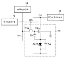
続いて、本開示の実施の形態に係る有機EL表示装置の構成例を説明する。図2は、本開示の実施の形態に係る有機EL表示装置の構成例を示す説明図である。以下、図2を用いて本開示の実施の形態に係る有機EL表示装置の構成例について説明する。
図4は、本開示の実施の形態に係る有機EL表示装置1の画素15の動作例をタイミングチャートで示す説明図である。以下、図4を用いて本開示の実施の形態に係る有機EL表示装置1の画素15の動作例について説明する。
本開示の実施の形態に係る有機EL表示装置1の画素15は、上述したように、映像信号書き込みトランジスタTsigには、Si半導体基板上に形成したMOSトランジスタを用い、駆動トランジスタTdrvにはTFTを用い、それぞれ使い分ける。
以上説明したように本開示の実施の形態によれば、駆動トランジスタと、映像信号書き込みトランジスタとでキャリア移動度が異なるトランジスタ、例えば、映像信号書き込みトランジスタには単結晶Si基板上に形成されたMOSトランジスタを用い、駆動トランジスタにはTFTを用いる、有機EL表示装置1が提供される。
(1)
発光部及び前記発光部を駆動するための駆動回路を備えた発光素子を複数有し、
前記駆動回路は、
前記発光部を制御する駆動トランジスタと、
映像信号の書き込みを制御する映像信号書き込みトランジスタと、
容量素子と、
を備え、
前記駆動トランジスタは、一方のソース・ドレイン領域が電流供給線に接続され、他方のソース・ドレイン領域が前記発光部及び前記容量素子の第1ノードに接続され、ゲート電極が前記容量素子の第2ノードに接続され、
前記映像信号書き込みトランジスタは、一方のソース・ドレイン領域がデータ線に接続され、他方のソース・ドレイン領域が前記駆動トランジスタのゲート電極及び前記容量素子の第2ノードに接続され、ゲート電極が走査線に接続され、
前記駆動トランジスタと、前記映像信号書き込みトランジスタとはキャリア移動度が異なる、表示装置。
(2)
前記駆動トランジスタのキャリア移動度は、前記映像信号書き込みトランジスタのキャリア移動度より低い、前記(1)に記載の表示装置。
(3)
前記映像信号書き込みトランジスタはシリコン半導体基板上に形成され、前記駆動トランジスタは薄膜トランジスタを用いる、前記(1)に記載の表示装置。
(4)
前記駆動トランジスタは、nチャネル型のMOSトランジスタである、前記(2)に記載の表示装置。
(5)
前記駆動トランジスタは配線層に形成される、前記(2)または(3)に記載の表示装置。
(6)
前記駆動トランジスタと前記映像信号書き込みトランジスタとは水平方向において少なくとも一部が重なる位置に形成される、前記(5)に記載の表示装置。
(7)
前記容量素子は、前記駆動トランジスタのソース・ドレイン領域を第1ノードとして、前記映像信号書き込みトランジスタのソース・ドレイン領域を第2ノードとする、前記(1)~(6)のいずれかに記載の表示装置。
(8)
前記容量素子は、MIS(Metal Insulator Semiconductor)キャパシタである前記(7)に記載の表示装置。
(9)
前記映像信号書き込みトランジスタのゲート酸化膜厚と、前記MISキャパシタの絶縁膜厚とが異なる、前記(8)に記載の表示装置。
(10)
前記(1)~(9)のいずれかに記載の表示装置を備える、電子機器。
11 :画素アレイ部
12 :ライトスキャナ
13 :ドライブスキャナ
14 :水平セレクタ
15 :画素
16 :信号線
32 :電源供給線
101 :Si基板
102 :酸化膜
103 :埋め込み酸化膜
111 :ソース・ドレイン領域
112 :ソース・ドレイン領域
113 :サイドウォール
114 :ゲート電極
115 :ゲート絶縁膜
121 :ソース・ドレイン領域
122 :ソース・ドレイン領域
124 :ゲート絶縁膜
125 :ゲート電極
131 :配線層間膜
132 :配線層間膜
133 :配線層間膜
134 :配線層間膜
135 :配線層間膜
136 :配線層間膜
140 :コンタクトホール及びコンタクトビア
151 :アノード電極
152 :有機材料層
153 :カソード電極
161 :電極
162 :電極
Cs :保持容量
Cel :補助容量
DS :電源供給線
Tdrv :駆動トランジスタ
Tsig :映像信号書き込みトランジスタ
WS :走査線
Claims (9)
- 発光部及び前記発光部を駆動するための駆動回路を備えた発光素子を複数有し、
前記駆動回路は、
前記発光部を制御する駆動トランジスタと、
シリコン半導体基板に形成されたMOSトランジスタにより構成されて映像信号の書き込みを制御する映像信号書き込みトランジスタと、
容量素子と、
を備え、
前記駆動トランジスタは、前記シリコン半導体基板に積層された配線層間膜に形成される薄膜トランジスタにより構成されて、一方のソース・ドレイン領域が電流供給線に接続され、他方のソース・ドレイン領域が前記発光部及び前記容量素子の第1ノードに接続され、ゲート電極が前記容量素子の第2ノードに接続され、
前記映像信号書き込みトランジスタは、一方のソース・ドレイン領域がデータ線に接続され、他方のソース・ドレイン領域が前記駆動トランジスタのゲート電極及び前記容量素子の第2ノードに接続され、ゲート電極が走査線に接続され、
前記駆動トランジスタは、前記映像信号書き込みトランジスタ及び前記容量素子とは異なる層に配置されるとともに前記シリコン半導体基板表面に対する法線方向から見て少なくとも一部が重なる位置に形成され、
前記駆動トランジスタのキャリア移動度は、前記映像信号書き込みトランジスタのキャリア移動度より低い、表示装置。 - 前記映像信号書き込みトランジスタは、nチャネル型のMOSトランジスタである、請求項1に記載の表示装置。
- 前記容量素子は、前記駆動トランジスタ及び前記映像信号書き込みトランジスタの間に配置される、請求項1に記載の表示装置。
- 前記容量素子は、MIMキャパシタである、請求項3に記載の表示装置。
- 前記容量素子は、前記シリコン半導体基板上に形成されるとともに前記映像信号書き込みトランジスタに隣接して配置される、請求項1に記載の表示装置。
- 前記容量素子は、MIS(Metal Insulator Semiconductor)キャパシタである、請求項5に記載の表示装置。
- 前記映像信号書き込みトランジスタのゲート酸化膜厚と、前記MISキャパシタの絶縁膜厚とが異なる、請求項6に記載の表示装置。
- 前記MISキャパシタは、10nm以下の膜厚の絶縁膜を備える、請求項6に記載の表示装置。
- 請求項1に記載の表示装置を備える、電子機器。
Applications Claiming Priority (3)
| Application Number | Priority Date | Filing Date | Title |
|---|---|---|---|
| JP2016085682 | 2016-04-22 | ||
| JP2016085682 | 2016-04-22 | ||
| PCT/JP2017/009691 WO2017183355A1 (ja) | 2016-04-22 | 2017-03-10 | 表示装置および電子機器 |
Publications (2)
| Publication Number | Publication Date |
|---|---|
| JPWO2017183355A1 JPWO2017183355A1 (ja) | 2019-02-28 |
| JP7100577B2 true JP7100577B2 (ja) | 2022-07-13 |
Family
ID=60116021
Family Applications (1)
| Application Number | Title | Priority Date | Filing Date |
|---|---|---|---|
| JP2018513064A Active JP7100577B2 (ja) | 2016-04-22 | 2017-03-10 | 表示装置および電子機器 |
Country Status (5)
| Country | Link |
|---|---|
| US (4) | US11081057B2 (ja) |
| JP (1) | JP7100577B2 (ja) |
| CN (3) | CN113936601A (ja) |
| DE (1) | DE112017002103B4 (ja) |
| WO (1) | WO2017183355A1 (ja) |
Families Citing this family (14)
| Publication number | Priority date | Publication date | Assignee | Title |
|---|---|---|---|---|
| CN106663394B (zh) * | 2014-07-23 | 2019-10-22 | 索尼公司 | 显示装置、制造显示装置的方法以及电子设备 |
| CN114155812A (zh) * | 2016-08-30 | 2022-03-08 | 索尼半导体解决方案公司 | 显示装置和电子设备 |
| JP7011449B2 (ja) | 2017-11-21 | 2022-01-26 | ソニーセミコンダクタソリューションズ株式会社 | 画素回路、表示装置および電子機器 |
| WO2020082390A1 (en) | 2018-10-27 | 2020-04-30 | Huawei Technologies Co., Ltd. | Sensor and display device |
| US11957017B2 (en) * | 2019-10-03 | 2024-04-09 | Sharp Kabushiki Kaisha | Display device |
| KR102779728B1 (ko) * | 2020-03-12 | 2025-03-12 | 삼성디스플레이 주식회사 | 표시 장치 및 그 구동 방법 |
| TWI744024B (zh) * | 2020-10-07 | 2021-10-21 | 聯嘉光電股份有限公司 | 一種微型發光二極體顯示器的晶粒結構 |
| EP4131239A4 (en) * | 2021-02-23 | 2023-05-24 | BOE Technology Group Co., Ltd. | DISPLAY PANEL AND DISPLAY DEVICE |
| CN112951824A (zh) * | 2021-02-25 | 2021-06-11 | 安徽熙泰智能科技有限公司 | 一种微显示用组合驱动芯片结构及其制作工艺 |
| CN113013163A (zh) * | 2021-02-25 | 2021-06-22 | 安徽熙泰智能科技有限公司 | 一种微显示驱动芯片结构及其制作工艺 |
| CN114005409B (zh) * | 2021-10-29 | 2022-11-25 | 绵阳惠科光电科技有限公司 | 像素驱动电路、方法及显示面板 |
| CN119384692A (zh) * | 2022-06-23 | 2025-01-28 | 索尼集团公司 | 显示装置及电子设备 |
| CN121713229A (zh) * | 2023-08-22 | 2026-03-20 | 索尼半导体解决方案公司 | 显示装置及电子设备 |
| KR20250143908A (ko) * | 2024-03-25 | 2025-10-10 | 삼성디스플레이 주식회사 | 픽셀 회로 및 이를 포함하는 표시 장치 |
Citations (3)
| Publication number | Priority date | Publication date | Assignee | Title |
|---|---|---|---|---|
| JP2005300786A (ja) | 2004-04-09 | 2005-10-27 | Sanyo Electric Co Ltd | 表示装置及びその製造方法 |
| JP2015194577A (ja) | 2014-03-31 | 2015-11-05 | ソニー株式会社 | 表示装置および電子機器 |
| US20160064421A1 (en) | 2014-08-29 | 2016-03-03 | Lg Display Co., Ltd. | Thin film transistor substrate and display device using the same |
Family Cites Families (51)
| Publication number | Priority date | Publication date | Assignee | Title |
|---|---|---|---|---|
| TW486869B (en) * | 1999-12-27 | 2002-05-11 | Sanyo Electric Co | Voltage producing circuit and a display device provided with such voltage producing circuit |
| US20030003665A1 (en) * | 2001-06-27 | 2003-01-02 | Nakagawa Osamu Samuel | Process for high-dielectric constant metal-insulator metal capacitor in VLSI multi-level metallization systems |
| JP3800050B2 (ja) * | 2001-08-09 | 2006-07-19 | 日本電気株式会社 | 表示装置の駆動回路 |
| KR100458710B1 (ko) * | 2001-11-06 | 2004-12-03 | 네오폴리((주)) | Oeld용 결정질 실리콘 박막트랜지스터 패널 및 제작방법 |
| US7230592B2 (en) * | 2002-03-04 | 2007-06-12 | Hitachi, Ltd. | Organic electroluminescent light emitting display device |
| JP4683825B2 (ja) * | 2002-04-24 | 2011-05-18 | 株式会社半導体エネルギー研究所 | 半導体装置およびその作製方法 |
| JP4128045B2 (ja) * | 2002-07-26 | 2008-07-30 | 三洋電機株式会社 | 有機elパネル |
| KR100466628B1 (ko) * | 2002-11-12 | 2005-01-15 | 삼성에스디아이 주식회사 | 평판표시장치 및 그의 제조방법 |
| JP2005308857A (ja) * | 2004-04-19 | 2005-11-04 | Sony Corp | アクティブマトリクス型表示装置およびその駆動方法 |
| TWI334313B (en) * | 2005-02-23 | 2010-12-01 | Au Optronics Corp | Organic electroluminiscent display and fabricating method thereof |
| JP2006284915A (ja) * | 2005-03-31 | 2006-10-19 | Toshiba Matsushita Display Technology Co Ltd | 表示装置及びアレイ基板 |
| TWI429327B (zh) * | 2005-06-30 | 2014-03-01 | Semiconductor Energy Lab | 半導體裝置、顯示裝置、及電子設備 |
| JP2007316510A (ja) * | 2006-05-29 | 2007-12-06 | Toshiba Matsushita Display Technology Co Ltd | アクティブマトリクス型表示装置 |
| JP2008046427A (ja) * | 2006-08-18 | 2008-02-28 | Sony Corp | 画像表示装置 |
| JP2008085091A (ja) * | 2006-09-28 | 2008-04-10 | Sony Corp | 薄膜トランジスタの製造方法、薄膜トランジスタ、および表示装置 |
| JP2008256916A (ja) * | 2007-04-04 | 2008-10-23 | Sony Corp | 有機エレクトロルミネッセンス発光部の駆動方法 |
| JP4479755B2 (ja) * | 2007-07-03 | 2010-06-09 | ソニー株式会社 | 有機エレクトロルミネッセンス素子、及び、有機エレクトロルミネッセンス表示装置 |
| JP5251034B2 (ja) * | 2007-08-15 | 2013-07-31 | ソニー株式会社 | 表示装置および電子機器 |
| JP4978435B2 (ja) * | 2007-11-14 | 2012-07-18 | ソニー株式会社 | 表示装置、表示装置の駆動方法および電子機器 |
| JP5181164B2 (ja) * | 2008-03-17 | 2013-04-10 | ユー・ディー・シー アイルランド リミテッド | 有機電界発光表示装置 |
| JP2009271200A (ja) * | 2008-05-01 | 2009-11-19 | Sony Corp | 表示装置及びその駆動方法 |
| KR101341011B1 (ko) * | 2008-05-17 | 2013-12-13 | 엘지디스플레이 주식회사 | 발광표시장치 |
| KR101681884B1 (ko) * | 2009-03-27 | 2016-12-05 | 가부시키가이샤 한도오따이 에네루기 켄큐쇼 | 반도체장치, 표시장치 및 전자기기 |
| KR101022652B1 (ko) * | 2009-04-02 | 2011-03-22 | 삼성모바일디스플레이주식회사 | 박막 트랜지스터 기판 제조방법 및 유기 발광 디스플레이 장치 제조방법 |
| JP2010243938A (ja) * | 2009-04-09 | 2010-10-28 | Sony Corp | 表示装置およびその駆動方法 |
| CN102439652B (zh) * | 2010-04-05 | 2015-05-06 | 松下电器产业株式会社 | 有机电致发光显示装置及其控制方法 |
| JP5644511B2 (ja) * | 2011-01-06 | 2014-12-24 | ソニー株式会社 | 有機el表示装置及び電子機器 |
| JP2012255874A (ja) | 2011-06-08 | 2012-12-27 | Sony Corp | 画素回路、表示装置、電子機器、及び、画素回路の駆動方法 |
| JP5891492B2 (ja) * | 2011-06-22 | 2016-03-23 | 株式会社Joled | 表示素子、表示装置、及び、電子機器 |
| JP5870546B2 (ja) * | 2011-08-23 | 2016-03-01 | ソニー株式会社 | 表示装置及び電子機器 |
| KR20130024029A (ko) * | 2011-08-30 | 2013-03-08 | 삼성디스플레이 주식회사 | 유기 발광 표시 장치 및 그 제조 방법 |
| JP5792745B2 (ja) * | 2011-10-28 | 2015-10-14 | 株式会社Joled | 薄膜半導体装置及び薄膜半導体装置の製造方法 |
| CN103582952B (zh) * | 2011-11-30 | 2016-08-03 | 株式会社日本有机雷特显示器 | 半导体器件和显示装置 |
| TW201324760A (zh) * | 2011-12-07 | 2013-06-16 | Chunghwa Picture Tubes Ltd | 畫素結構及其製造方法 |
| JP2013168341A (ja) | 2012-02-17 | 2013-08-29 | Seiko Epson Corp | 有機el装置および電子機器 |
| JP6056175B2 (ja) * | 2012-04-03 | 2017-01-11 | セイコーエプソン株式会社 | 電気光学装置及び電子機器 |
| US9190525B2 (en) * | 2012-07-06 | 2015-11-17 | Semiconductor Energy Laboratory Co., Ltd. | Semiconductor device including oxide semiconductor layer |
| JP6031652B2 (ja) * | 2012-08-31 | 2016-11-24 | 株式会社Joled | 表示装置及び電子機器 |
| JP6286941B2 (ja) | 2013-08-27 | 2018-03-07 | セイコーエプソン株式会社 | 発光装置、発光装置の製造方法、電子機器 |
| JP5770236B2 (ja) * | 2013-09-18 | 2015-08-26 | 株式会社ジャパンディスプレイ | 表示装置 |
| US9083320B2 (en) * | 2013-09-20 | 2015-07-14 | Maofeng YANG | Apparatus and method for electrical stability compensation |
| KR20160102295A (ko) * | 2013-12-26 | 2016-08-29 | 가부시키가이샤 한도오따이 에네루기 켄큐쇼 | 반도체 장치 |
| JP6474648B2 (ja) * | 2014-03-07 | 2019-02-27 | 株式会社半導体エネルギー研究所 | 検知器および入力装置 |
| TWI663726B (zh) | 2014-05-30 | 2019-06-21 | Semiconductor Energy Laboratory Co., Ltd. | 半導體裝置、模組及電子裝置 |
| US9362320B2 (en) * | 2014-06-03 | 2016-06-07 | Taiwan Semiconductor Manufacturing Company, Ltd. | Integrated circuit having a level shifter and method of making the same |
| KR102298336B1 (ko) * | 2014-06-20 | 2021-09-08 | 엘지디스플레이 주식회사 | 유기발광다이오드 표시장치 |
| KR102296945B1 (ko) * | 2014-07-04 | 2021-09-01 | 엘지디스플레이 주식회사 | 유기 발광 표시 장치 및 그 제조 방법 |
| US10181573B2 (en) * | 2014-07-11 | 2019-01-15 | Lg Display Co., Ltd. | Organic light-emitting diode display device and method of fabricating the same |
| CN104201188B (zh) | 2014-08-22 | 2017-07-25 | 京东方科技集团股份有限公司 | Oled像素单元及其制备方法、显示面板和显示装置 |
| KR102289838B1 (ko) * | 2015-04-28 | 2021-08-13 | 삼성디스플레이 주식회사 | 유기 발광 표시 장치 |
| KR102663039B1 (ko) * | 2017-02-28 | 2024-05-07 | 엘지디스플레이 주식회사 | 전계 발광 표시장치 |
-
2017
- 2017-03-10 CN CN202111209606.2A patent/CN113936601A/zh active Pending
- 2017-03-10 JP JP2018513064A patent/JP7100577B2/ja active Active
- 2017-03-10 US US16/088,162 patent/US11081057B2/en active Active
- 2017-03-10 CN CN202111209345.4A patent/CN113948560A/zh active Pending
- 2017-03-10 WO PCT/JP2017/009691 patent/WO2017183355A1/ja not_active Ceased
- 2017-03-10 CN CN201780023790.7A patent/CN109074765B/zh active Active
- 2017-03-10 DE DE112017002103.0T patent/DE112017002103B4/de active Active
-
2021
- 2021-07-20 US US17/380,346 patent/US11710456B2/en active Active
-
2023
- 2023-06-20 US US18/337,754 patent/US12148392B2/en active Active
-
2024
- 2024-10-17 US US18/918,496 patent/US20250037671A1/en active Pending
Patent Citations (3)
| Publication number | Priority date | Publication date | Assignee | Title |
|---|---|---|---|---|
| JP2005300786A (ja) | 2004-04-09 | 2005-10-27 | Sanyo Electric Co Ltd | 表示装置及びその製造方法 |
| JP2015194577A (ja) | 2014-03-31 | 2015-11-05 | ソニー株式会社 | 表示装置および電子機器 |
| US20160064421A1 (en) | 2014-08-29 | 2016-03-03 | Lg Display Co., Ltd. | Thin film transistor substrate and display device using the same |
Also Published As
| Publication number | Publication date |
|---|---|
| US11081057B2 (en) | 2021-08-03 |
| JPWO2017183355A1 (ja) | 2019-02-28 |
| CN113936601A (zh) | 2022-01-14 |
| US20250037671A1 (en) | 2025-01-30 |
| US12148392B2 (en) | 2024-11-19 |
| US20200302873A1 (en) | 2020-09-24 |
| DE112017002103B4 (de) | 2022-06-15 |
| US11710456B2 (en) | 2023-07-25 |
| CN109074765A (zh) | 2018-12-21 |
| CN109074765B (zh) | 2021-11-05 |
| CN113948560A (zh) | 2022-01-18 |
| US20240038178A1 (en) | 2024-02-01 |
| DE112017002103T5 (de) | 2019-01-03 |
| US20220028343A1 (en) | 2022-01-27 |
| WO2017183355A1 (ja) | 2017-10-26 |
Similar Documents
| Publication | Publication Date | Title |
|---|---|---|
| US12148392B2 (en) | Display apparatus and electronic device | |
| KR102245043B1 (ko) | 표시 장치 | |
| US10559256B2 (en) | Pixel driver circuitry for a display device | |
| US9792860B2 (en) | Light-emitting element, display device and electronic apparatus | |
| TWI633529B (zh) | 顯示器、顯示器驅動電路、顯示器驅動方法及電子設備 | |
| WO2020001026A1 (zh) | 像素驱动电路及方法、显示面板 | |
| CN101271665B (zh) | 用于有机电致发光发光部的驱动方法 | |
| US12315444B2 (en) | Pixel circuit, display device, and electronic apparatus | |
| JP2014160203A (ja) | 表示装置およびその駆動方法、並びに電子機器 | |
| US10985216B2 (en) | Display apparatus and imaging apparatus | |
| CN221008952U (zh) | 显示装置 | |
| JP2014163972A (ja) | 表示装置およびその駆動方法、並びに電子機器 | |
| WO2025194446A1 (zh) | 像素驱动电路及其驱动方法、显示装置 |
Legal Events
| Date | Code | Title | Description |
|---|---|---|---|
| RD04 | Notification of resignation of power of attorney |
Free format text: JAPANESE INTERMEDIATE CODE: A7424 Effective date: 20190208 |
|
| RD03 | Notification of appointment of power of attorney |
Free format text: JAPANESE INTERMEDIATE CODE: A7423 Effective date: 20190214 |
|
| RD04 | Notification of resignation of power of attorney |
Free format text: JAPANESE INTERMEDIATE CODE: A7424 Effective date: 20190222 |
|
| RD02 | Notification of acceptance of power of attorney |
Free format text: JAPANESE INTERMEDIATE CODE: A7422 Effective date: 20190515 |
|
| RD04 | Notification of resignation of power of attorney |
Free format text: JAPANESE INTERMEDIATE CODE: A7424 Effective date: 20190522 |
|
| A621 | Written request for application examination |
Free format text: JAPANESE INTERMEDIATE CODE: A621 Effective date: 20200302 |
|
| A131 | Notification of reasons for refusal |
Free format text: JAPANESE INTERMEDIATE CODE: A131 Effective date: 20200915 |
|
| A521 | Request for written amendment filed |
Free format text: JAPANESE INTERMEDIATE CODE: A523 Effective date: 20201027 |
|
| A02 | Decision of refusal |
Free format text: JAPANESE INTERMEDIATE CODE: A02 Effective date: 20210202 |
|
| A521 | Request for written amendment filed |
Free format text: JAPANESE INTERMEDIATE CODE: A523 Effective date: 20210506 |
|
| C60 | Trial request (containing other claim documents, opposition documents) |
Free format text: JAPANESE INTERMEDIATE CODE: C60 Effective date: 20210506 |
|
| A911 | Transfer to examiner for re-examination before appeal (zenchi) |
Free format text: JAPANESE INTERMEDIATE CODE: A911 Effective date: 20210513 |
|
| C21 | Notice of transfer of a case for reconsideration by examiners before appeal proceedings |
Free format text: JAPANESE INTERMEDIATE CODE: C21 Effective date: 20210518 |
|
| A912 | Re-examination (zenchi) completed and case transferred to appeal board |
Free format text: JAPANESE INTERMEDIATE CODE: A912 Effective date: 20210604 |
|
| C211 | Notice of termination of reconsideration by examiners before appeal proceedings |
Free format text: JAPANESE INTERMEDIATE CODE: C211 Effective date: 20210608 |
|
| C22 | Notice of designation (change) of administrative judge |
Free format text: JAPANESE INTERMEDIATE CODE: C22 Effective date: 20211019 |
|
| C13 | Notice of reasons for refusal |
Free format text: JAPANESE INTERMEDIATE CODE: C13 Effective date: 20220201 |
|
| C19 | Decision taken to dismiss amendment |
Free format text: JAPANESE INTERMEDIATE CODE: C19 Effective date: 20220215 |
|
| C30A | Notification sent |
Free format text: JAPANESE INTERMEDIATE CODE: C3012 Effective date: 20220215 |
|
| A521 | Request for written amendment filed |
Free format text: JAPANESE INTERMEDIATE CODE: A523 Effective date: 20220404 |
|
| C22 | Notice of designation (change) of administrative judge |
Free format text: JAPANESE INTERMEDIATE CODE: C22 Effective date: 20220426 |
|
| C23 | Notice of termination of proceedings |
Free format text: JAPANESE INTERMEDIATE CODE: C23 Effective date: 20220510 |
|
| C03 | Trial/appeal decision taken |
Free format text: JAPANESE INTERMEDIATE CODE: C03 Effective date: 20220607 |
|
| C30A | Notification sent |
Free format text: JAPANESE INTERMEDIATE CODE: C3012 Effective date: 20220607 |
|
| A61 | First payment of annual fees (during grant procedure) |
Free format text: JAPANESE INTERMEDIATE CODE: A61 Effective date: 20220701 |
|
| R150 | Certificate of patent or registration of utility model |
Ref document number: 7100577 Country of ref document: JP Free format text: JAPANESE INTERMEDIATE CODE: R150 |