JP7216623B2 - 半導体チップ - Google Patents
半導体チップ Download PDFInfo
- Publication number
- JP7216623B2 JP7216623B2 JP2019146036A JP2019146036A JP7216623B2 JP 7216623 B2 JP7216623 B2 JP 7216623B2 JP 2019146036 A JP2019146036 A JP 2019146036A JP 2019146036 A JP2019146036 A JP 2019146036A JP 7216623 B2 JP7216623 B2 JP 7216623B2
- Authority
- JP
- Japan
- Prior art keywords
- semiconductor chip
- thin film
- semiconductor
- semiconductor substrate
- present
- Prior art date
- Legal status (The legal status is an assumption and is not a legal conclusion. Google has not performed a legal analysis and makes no representation as to the accuracy of the status listed.)
- Active
Links
Images




Classifications
-
- H—ELECTRICITY
- H10—SEMICONDUCTOR DEVICES; ELECTRIC SOLID-STATE DEVICES NOT OTHERWISE PROVIDED FOR
- H10W—GENERIC PACKAGES, INTERCONNECTIONS, CONNECTORS OR OTHER CONSTRUCTIONAL DETAILS OF DEVICES COVERED BY CLASS H10
- H10W42/00—Arrangements for protection of devices
- H10W42/121—Arrangements for protection of devices protecting against mechanical damage
-
- B—PERFORMING OPERATIONS; TRANSPORTING
- B06—GENERATING OR TRANSMITTING MECHANICAL VIBRATIONS IN GENERAL
- B06B—METHODS OR APPARATUS FOR GENERATING OR TRANSMITTING MECHANICAL VIBRATIONS OF INFRASONIC, SONIC, OR ULTRASONIC FREQUENCY, e.g. FOR PERFORMING MECHANICAL WORK IN GENERAL
- B06B1/00—Methods or apparatus for generating mechanical vibrations of infrasonic, sonic, or ultrasonic frequency
- B06B1/02—Methods or apparatus for generating mechanical vibrations of infrasonic, sonic, or ultrasonic frequency making use of electrical energy
- B06B1/0292—Electrostatic transducers, e.g. electret-type
-
- B—PERFORMING OPERATIONS; TRANSPORTING
- B81—MICROSTRUCTURAL TECHNOLOGY
- B81B—MICROSTRUCTURAL DEVICES OR SYSTEMS, e.g. MICROMECHANICAL DEVICES
- B81B3/00—Devices comprising flexible or deformable elements, e.g. comprising elastic tongues or membranes
- B81B3/0064—Constitution or structural means for improving or controlling the physical properties of a device
- B81B3/0067—Mechanical properties
- B81B3/0072—For controlling internal stress or strain in moving or flexible elements, e.g. stress compensating layers
-
- H—ELECTRICITY
- H10—SEMICONDUCTOR DEVICES; ELECTRIC SOLID-STATE DEVICES NOT OTHERWISE PROVIDED FOR
- H10W—GENERIC PACKAGES, INTERCONNECTIONS, CONNECTORS OR OTHER CONSTRUCTIONAL DETAILS OF DEVICES COVERED BY CLASS H10
- H10W74/00—Encapsulations, e.g. protective coatings
- H10W74/10—Encapsulations, e.g. protective coatings characterised by their shape or disposition
- H10W74/131—Encapsulations, e.g. protective coatings characterised by their shape or disposition the semiconductor body being only partially enclosed
-
- A—HUMAN NECESSITIES
- A61—MEDICAL OR VETERINARY SCIENCE; HYGIENE
- A61B—DIAGNOSIS; SURGERY; IDENTIFICATION
- A61B8/00—Diagnosis using ultrasonic, sonic or infrasonic waves
- A61B8/12—Diagnosis using ultrasonic, sonic or infrasonic waves in body cavities or body tracts, e.g. by using catheters
-
- A—HUMAN NECESSITIES
- A61—MEDICAL OR VETERINARY SCIENCE; HYGIENE
- A61B—DIAGNOSIS; SURGERY; IDENTIFICATION
- A61B8/00—Diagnosis using ultrasonic, sonic or infrasonic waves
- A61B8/44—Constructional features of the ultrasonic, sonic or infrasonic diagnostic device
- A61B8/4444—Constructional features of the ultrasonic, sonic or infrasonic diagnostic device related to the probe
- A61B8/445—Details of catheter construction
-
- A—HUMAN NECESSITIES
- A61—MEDICAL OR VETERINARY SCIENCE; HYGIENE
- A61B—DIAGNOSIS; SURGERY; IDENTIFICATION
- A61B8/00—Diagnosis using ultrasonic, sonic or infrasonic waves
- A61B8/44—Constructional features of the ultrasonic, sonic or infrasonic diagnostic device
- A61B8/4483—Constructional features of the ultrasonic, sonic or infrasonic diagnostic device characterised by features of the ultrasound transducer
-
- B—PERFORMING OPERATIONS; TRANSPORTING
- B81—MICROSTRUCTURAL TECHNOLOGY
- B81B—MICROSTRUCTURAL DEVICES OR SYSTEMS, e.g. MICROMECHANICAL DEVICES
- B81B2201/00—Specific applications of microelectromechanical systems
- B81B2201/02—Sensors
- B81B2201/0271—Resonators; ultrasonic resonators
Landscapes
- Engineering & Computer Science (AREA)
- Mechanical Engineering (AREA)
- Computer Hardware Design (AREA)
- Microelectronics & Electronic Packaging (AREA)
- Transducers For Ultrasonic Waves (AREA)
- Semiconductor Integrated Circuits (AREA)
- Micromachines (AREA)
Description

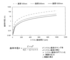
E:シリコン基板(すなわち半導体基板101)のヤング率
d:シリコン基板の厚さ
ν:シリコン基板のポワソン比
σ:薄膜102の応力
t:薄膜102の厚さ
である。
101 半導体基板
102 内部応力を持つ薄膜
103 半導体デバイス
Claims (5)
- 半導体チップであって、
半導体基板と、前記半導体基板の上に形成された内部応力を持つ薄膜と、前記薄膜が形成された前記半導体基板の上に形成された半導体デバイスと、を有し、
前記薄膜の内部応力によって湾曲し、
前記半導体基板の上に、前記半導体チップが湾曲する方向と直交する方向に整列した複数の前記薄膜のパターンが形成されることを特徴とする半導体チップ。 - 請求項1に記載の半導体チップであって、
前記薄膜は、前記半導体基板に接して形成されることを特徴とする半導体チップ。 - 請求項1に記載の半導体チップであって、
各々の前記薄膜のパターンの前記半導体チップが湾曲する方向のサイズは、前記半導体チップが湾曲する方向と直交する方向のサイズより大きいことを特徴とする半導体チップ。 - 請求項1に記載の半導体チップであって、
前記半導体デバイスは、静電容量型の超音波トランスデューサであることを特徴とする半導体チップ。 - 請求項4に記載の半導体チップであって、
前記半導体デバイスが形成される層に、前記静電容量型の超音波トランスデューサの複数のセルが形成され、
前記半導体デバイスが形成される層の前記複数のセル間を区切る位置に溝が形成されることを特徴とする半導体チップ。
Priority Applications (2)
| Application Number | Priority Date | Filing Date | Title |
|---|---|---|---|
| JP2019146036A JP7216623B2 (ja) | 2019-08-08 | 2019-08-08 | 半導体チップ |
| US16/928,909 US11502046B2 (en) | 2019-08-08 | 2020-07-14 | Semiconductor chip |
Applications Claiming Priority (1)
| Application Number | Priority Date | Filing Date | Title |
|---|---|---|---|
| JP2019146036A JP7216623B2 (ja) | 2019-08-08 | 2019-08-08 | 半導体チップ |
Publications (2)
| Publication Number | Publication Date |
|---|---|
| JP2021027538A JP2021027538A (ja) | 2021-02-22 |
| JP7216623B2 true JP7216623B2 (ja) | 2023-02-01 |
Family
ID=74498957
Family Applications (1)
| Application Number | Title | Priority Date | Filing Date |
|---|---|---|---|
| JP2019146036A Active JP7216623B2 (ja) | 2019-08-08 | 2019-08-08 | 半導体チップ |
Country Status (2)
| Country | Link |
|---|---|
| US (1) | US11502046B2 (ja) |
| JP (1) | JP7216623B2 (ja) |
Families Citing this family (1)
| Publication number | Priority date | Publication date | Assignee | Title |
|---|---|---|---|---|
| DE102021129855A1 (de) * | 2021-11-16 | 2023-05-17 | Infineon Technologies Ag | Ultraschallberührungssensor |
Citations (3)
| Publication number | Priority date | Publication date | Assignee | Title |
|---|---|---|---|---|
| JP2005210710A (ja) | 2003-12-31 | 2005-08-04 | General Electric Co <Ge> | マイクロマシン加工した湾曲超音波トランスジューサ・アレイ並びに関連する製造方法 |
| JP2013141524A (ja) | 2012-01-11 | 2013-07-22 | Seiko Epson Corp | 超音波トランスデューサー、超音波プローブ、診断機器および電子機器 |
| JP2018183426A (ja) | 2017-04-26 | 2018-11-22 | 株式会社日立製作所 | 超音波撮像装置並びに超音波トランスデューサおよびその製造方法 |
Family Cites Families (9)
| Publication number | Priority date | Publication date | Assignee | Title |
|---|---|---|---|---|
| JP3400329B2 (ja) * | 1998-01-07 | 2003-04-28 | 日本電信電話株式会社 | 半導体装置 |
| WO2008120705A1 (ja) * | 2007-03-29 | 2008-10-09 | Nec Corporation | 半導体装置 |
| US8954156B2 (en) | 2010-10-27 | 2015-02-10 | National Tsing Hua University | Methods and apparatuses for configuring artificial retina devices |
| US20120109255A1 (en) | 2010-10-27 | 2012-05-03 | National Tsing Hua University | Retina Stimulation Apparatus and Manufacturing Method Thereof |
| US9114004B2 (en) | 2010-10-27 | 2015-08-25 | Iridium Medical Technology Co, Ltd. | Flexible artificial retina devices |
| US8530265B2 (en) | 2010-10-27 | 2013-09-10 | National Tsing Hua University | Method of fabricating flexible artificial retina devices |
| US9155881B2 (en) | 2011-05-06 | 2015-10-13 | Iridium Medical Technology Co, Ltd. | Non-planar chip assembly |
| WO2012154211A1 (en) | 2011-05-06 | 2012-11-15 | National Tsing Hua University | Non-planar chip assembly |
| US8613135B2 (en) | 2011-05-06 | 2013-12-24 | National Tsing Hua University | Method for non-planar chip assembly |
-
2019
- 2019-08-08 JP JP2019146036A patent/JP7216623B2/ja active Active
-
2020
- 2020-07-14 US US16/928,909 patent/US11502046B2/en active Active
Patent Citations (3)
| Publication number | Priority date | Publication date | Assignee | Title |
|---|---|---|---|---|
| JP2005210710A (ja) | 2003-12-31 | 2005-08-04 | General Electric Co <Ge> | マイクロマシン加工した湾曲超音波トランスジューサ・アレイ並びに関連する製造方法 |
| JP2013141524A (ja) | 2012-01-11 | 2013-07-22 | Seiko Epson Corp | 超音波トランスデューサー、超音波プローブ、診断機器および電子機器 |
| JP2018183426A (ja) | 2017-04-26 | 2018-11-22 | 株式会社日立製作所 | 超音波撮像装置並びに超音波トランスデューサおよびその製造方法 |
Also Published As
| Publication number | Publication date |
|---|---|
| US20210043584A1 (en) | 2021-02-11 |
| JP2021027538A (ja) | 2021-02-22 |
| US11502046B2 (en) | 2022-11-15 |
Similar Documents
| Publication | Publication Date | Title |
|---|---|---|
| KR101954102B1 (ko) | 정전용량형 트랜스듀서, 정전용량형 트랜스듀서 제조 방법 및 피검체 정보취득장치 | |
| US7667374B2 (en) | Ultrasonic transducer, ultrasonic probe and method for fabricating the same | |
| CN102728535B (zh) | 电气机械换能器及其制造方法 | |
| KR101561661B1 (ko) | 진동막에 부착된 질량체를 가진 압전형 마이크로 스피커 및 그 제조 방법 | |
| US20110215672A1 (en) | Mems device | |
| US7285897B2 (en) | Curved micromachined ultrasonic transducer arrays and related methods of manufacture | |
| JP5178791B2 (ja) | 静電容量型超音波振動子 | |
| JP6123171B2 (ja) | 超音波トランスデューサー、超音波プローブおよび超音波検査装置 | |
| US8858447B2 (en) | Ultrasonic transducer and method of manufacturing the same | |
| WO2016047186A1 (ja) | 超音波トランスデューサ、その製造方法、超音波トランスデューサアレイ及び超音波検査装置 | |
| JP7772148B2 (ja) | 圧電素子、圧電装置 | |
| Sadeghpour et al. | Flexible soi-based piezoelectric micromachined ultrasound transducer (PMUT) arrays | |
| CN112485775A (zh) | 换能装置、换能结构及其制造方法 | |
| KR100791821B1 (ko) | 용량성 초음파 변환기 및 그것의 제조방법 | |
| US11762192B2 (en) | Optical scanning device and method of manufacturing the same | |
| JP6606034B2 (ja) | 容量検出型超音波トランスデューサおよびそれを備えた超音波撮像装置 | |
| US11502046B2 (en) | Semiconductor chip | |
| JP4640249B2 (ja) | 超音波センサ | |
| JP7816794B2 (ja) | 可撓性超音波プローブヘッド、超音波プローブ、及び超音波診断装置 | |
| CN114105082B (zh) | 压电微机械超声波换能器及其制作方法 | |
| JP7660664B2 (ja) | 超音波トランスデューサ、測距装置および超音波トランスデューサの製造方法 | |
| JP2010156591A (ja) | Memsセンサおよびmemsセンサの製造方法 | |
| CN117985648A (zh) | 压电mems换能器及其加工方法、封装结构及电子设备 |
Legal Events
| Date | Code | Title | Description |
|---|---|---|---|
| A621 | Written request for application examination |
Free format text: JAPANESE INTERMEDIATE CODE: A621 Effective date: 20211008 |
|
| A977 | Report on retrieval |
Free format text: JAPANESE INTERMEDIATE CODE: A971007 Effective date: 20220802 |
|
| A131 | Notification of reasons for refusal |
Free format text: JAPANESE INTERMEDIATE CODE: A131 Effective date: 20220809 |
|
| A521 | Request for written amendment filed |
Free format text: JAPANESE INTERMEDIATE CODE: A523 Effective date: 20220922 |
|
| TRDD | Decision of grant or rejection written | ||
| A01 | Written decision to grant a patent or to grant a registration (utility model) |
Free format text: JAPANESE INTERMEDIATE CODE: A01 Effective date: 20230117 |
|
| A61 | First payment of annual fees (during grant procedure) |
Free format text: JAPANESE INTERMEDIATE CODE: A61 Effective date: 20230120 |
|
| R150 | Certificate of patent or registration of utility model |
Ref document number: 7216623 Country of ref document: JP Free format text: JAPANESE INTERMEDIATE CODE: R150 |