JP7247681B2 - 半導体組立体 - Google Patents
半導体組立体 Download PDFInfo
- Publication number
- JP7247681B2 JP7247681B2 JP2019049921A JP2019049921A JP7247681B2 JP 7247681 B2 JP7247681 B2 JP 7247681B2 JP 2019049921 A JP2019049921 A JP 2019049921A JP 2019049921 A JP2019049921 A JP 2019049921A JP 7247681 B2 JP7247681 B2 JP 7247681B2
- Authority
- JP
- Japan
- Prior art keywords
- insulating layer
- semiconductor
- semiconductor chip
- electrode
- anode wiring
- Prior art date
- Legal status (The legal status is an assumption and is not a legal conclusion. Google has not performed a legal analysis and makes no representation as to the accuracy of the status listed.)
- Active
Links
Images

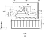


Classifications
-
- H—ELECTRICITY
- H10—SEMICONDUCTOR DEVICES; ELECTRIC SOLID-STATE DEVICES NOT OTHERWISE PROVIDED FOR
- H10W—GENERIC PACKAGES, INTERCONNECTIONS, CONNECTORS OR OTHER CONSTRUCTIONAL DETAILS OF DEVICES COVERED BY CLASS H10
- H10W40/00—Arrangements for thermal protection or thermal control
- H10W40/20—Arrangements for cooling
- H10W40/25—Arrangements for cooling characterised by their materials
- H10W40/255—Arrangements for cooling characterised by their materials having a laminate or multilayered structure, e.g. direct bond copper [DBC] ceramic substrates
-
- H—ELECTRICITY
- H10—SEMICONDUCTOR DEVICES; ELECTRIC SOLID-STATE DEVICES NOT OTHERWISE PROVIDED FOR
- H10P—GENERIC PROCESSES OR APPARATUS FOR THE MANUFACTURE OR TREATMENT OF DEVICES COVERED BY CLASS H10
- H10P74/00—Testing or measuring during manufacture or treatment of wafers, substrates or devices
- H10P74/27—Structural arrangements therefor
-
- G—PHYSICS
- G01—MEASURING; TESTING
- G01K—MEASURING TEMPERATURE; MEASURING QUANTITY OF HEAT; THERMALLY-SENSITIVE ELEMENTS NOT OTHERWISE PROVIDED FOR
- G01K7/00—Measuring temperature based on the use of electric or magnetic elements directly sensitive to heat ; Power supply therefor, e.g. using thermoelectric elements
- G01K7/01—Measuring temperature based on the use of electric or magnetic elements directly sensitive to heat ; Power supply therefor, e.g. using thermoelectric elements using semiconducting elements having PN junctions
-
- H—ELECTRICITY
- H10—SEMICONDUCTOR DEVICES; ELECTRIC SOLID-STATE DEVICES NOT OTHERWISE PROVIDED FOR
- H10W—GENERIC PACKAGES, INTERCONNECTIONS, CONNECTORS OR OTHER CONSTRUCTIONAL DETAILS OF DEVICES COVERED BY CLASS H10
- H10W40/00—Arrangements for thermal protection or thermal control
-
- H—ELECTRICITY
- H10—SEMICONDUCTOR DEVICES; ELECTRIC SOLID-STATE DEVICES NOT OTHERWISE PROVIDED FOR
- H10W—GENERIC PACKAGES, INTERCONNECTIONS, CONNECTORS OR OTHER CONSTRUCTIONAL DETAILS OF DEVICES COVERED BY CLASS H10
- H10W40/00—Arrangements for thermal protection or thermal control
- H10W40/10—Arrangements for heating
-
- H—ELECTRICITY
- H10—SEMICONDUCTOR DEVICES; ELECTRIC SOLID-STATE DEVICES NOT OTHERWISE PROVIDED FOR
- H10W—GENERIC PACKAGES, INTERCONNECTIONS, CONNECTORS OR OTHER CONSTRUCTIONAL DETAILS OF DEVICES COVERED BY CLASS H10
- H10W70/00—Package substrates; Interposers; Redistribution layers [RDL]
- H10W70/20—Conductive package substrates serving as an interconnection, e.g. metal plates
-
- H—ELECTRICITY
- H10—SEMICONDUCTOR DEVICES; ELECTRIC SOLID-STATE DEVICES NOT OTHERWISE PROVIDED FOR
- H10W—GENERIC PACKAGES, INTERCONNECTIONS, CONNECTORS OR OTHER CONSTRUCTIONAL DETAILS OF DEVICES COVERED BY CLASS H10
- H10W76/00—Containers; Fillings or auxiliary members therefor; Seals
- H10W76/10—Containers or parts thereof
- H10W76/12—Containers or parts thereof characterised by their shape
- H10W76/15—Containers comprising an insulating or insulated base
-
- H—ELECTRICITY
- H10—SEMICONDUCTOR DEVICES; ELECTRIC SOLID-STATE DEVICES NOT OTHERWISE PROVIDED FOR
- H10W—GENERIC PACKAGES, INTERCONNECTIONS, CONNECTORS OR OTHER CONSTRUCTIONAL DETAILS OF DEVICES COVERED BY CLASS H10
- H10W76/00—Containers; Fillings or auxiliary members therefor; Seals
- H10W76/40—Fillings or auxiliary members in containers, e.g. centering rings
- H10W76/42—Fillings
- H10W76/47—Solid or gel fillings
-
- H—ELECTRICITY
- H10—SEMICONDUCTOR DEVICES; ELECTRIC SOLID-STATE DEVICES NOT OTHERWISE PROVIDED FOR
- H10P—GENERIC PROCESSES OR APPARATUS FOR THE MANUFACTURE OR TREATMENT OF DEVICES COVERED BY CLASS H10
- H10P74/00—Testing or measuring during manufacture or treatment of wafers, substrates or devices
- H10P74/27—Structural arrangements therefor
- H10P74/277—Circuits for electrically characterising or monitoring manufacturing processes, e.g. circuits in tested chips or circuits in testing wafers
-
- H—ELECTRICITY
- H10—SEMICONDUCTOR DEVICES; ELECTRIC SOLID-STATE DEVICES NOT OTHERWISE PROVIDED FOR
- H10W—GENERIC PACKAGES, INTERCONNECTIONS, CONNECTORS OR OTHER CONSTRUCTIONAL DETAILS OF DEVICES COVERED BY CLASS H10
- H10W70/00—Package substrates; Interposers; Redistribution layers [RDL]
- H10W70/60—Insulating or insulated package substrates; Interposers; Redistribution layers
- H10W70/62—Insulating or insulated package substrates; Interposers; Redistribution layers characterised by their interconnections
- H10W70/65—Shapes or dispositions of interconnections
-
- H—ELECTRICITY
- H10—SEMICONDUCTOR DEVICES; ELECTRIC SOLID-STATE DEVICES NOT OTHERWISE PROVIDED FOR
- H10W—GENERIC PACKAGES, INTERCONNECTIONS, CONNECTORS OR OTHER CONSTRUCTIONAL DETAILS OF DEVICES COVERED BY CLASS H10
- H10W72/00—Interconnections or connectors in packages
- H10W72/30—Die-attach connectors
- H10W72/381—Auxiliary members
- H10W72/387—Flow barriers
-
- H—ELECTRICITY
- H10—SEMICONDUCTOR DEVICES; ELECTRIC SOLID-STATE DEVICES NOT OTHERWISE PROVIDED FOR
- H10W—GENERIC PACKAGES, INTERCONNECTIONS, CONNECTORS OR OTHER CONSTRUCTIONAL DETAILS OF DEVICES COVERED BY CLASS H10
- H10W72/00—Interconnections or connectors in packages
- H10W72/60—Strap connectors, e.g. thick copper clips for grounding of power devices
- H10W72/641—Dispositions of strap connectors
- H10W72/646—Dispositions of strap connectors the connected ends being on auxiliary connecting means on bond pads, e.g. on a bump connector
-
- H—ELECTRICITY
- H10—SEMICONDUCTOR DEVICES; ELECTRIC SOLID-STATE DEVICES NOT OTHERWISE PROVIDED FOR
- H10W—GENERIC PACKAGES, INTERCONNECTIONS, CONNECTORS OR OTHER CONSTRUCTIONAL DETAILS OF DEVICES COVERED BY CLASS H10
- H10W72/00—Interconnections or connectors in packages
- H10W72/60—Strap connectors, e.g. thick copper clips for grounding of power devices
- H10W72/681—Auxiliary members, e.g. flow barriers
-
- H—ELECTRICITY
- H10—SEMICONDUCTOR DEVICES; ELECTRIC SOLID-STATE DEVICES NOT OTHERWISE PROVIDED FOR
- H10W—GENERIC PACKAGES, INTERCONNECTIONS, CONNECTORS OR OTHER CONSTRUCTIONAL DETAILS OF DEVICES COVERED BY CLASS H10
- H10W72/00—Interconnections or connectors in packages
- H10W72/90—Bond pads, in general
-
- H—ELECTRICITY
- H10—SEMICONDUCTOR DEVICES; ELECTRIC SOLID-STATE DEVICES NOT OTHERWISE PROVIDED FOR
- H10W—GENERIC PACKAGES, INTERCONNECTIONS, CONNECTORS OR OTHER CONSTRUCTIONAL DETAILS OF DEVICES COVERED BY CLASS H10
- H10W90/00—Package configurations
- H10W90/701—Package configurations characterised by the relative positions of pads or connectors relative to package parts
- H10W90/731—Package configurations characterised by the relative positions of pads or connectors relative to package parts of die-attach connectors
- H10W90/734—Package configurations characterised by the relative positions of pads or connectors relative to package parts of die-attach connectors between a chip and a stacked insulating package substrate, interposer or RDL
-
- H—ELECTRICITY
- H10—SEMICONDUCTOR DEVICES; ELECTRIC SOLID-STATE DEVICES NOT OTHERWISE PROVIDED FOR
- H10W—GENERIC PACKAGES, INTERCONNECTIONS, CONNECTORS OR OTHER CONSTRUCTIONAL DETAILS OF DEVICES COVERED BY CLASS H10
- H10W90/00—Package configurations
- H10W90/701—Package configurations characterised by the relative positions of pads or connectors relative to package parts
- H10W90/751—Package configurations characterised by the relative positions of pads or connectors relative to package parts of bond wires
- H10W90/756—Package configurations characterised by the relative positions of pads or connectors relative to package parts of bond wires between a chip and a stacked lead frame, conducting package substrate or heat sink
-
- H—ELECTRICITY
- H10—SEMICONDUCTOR DEVICES; ELECTRIC SOLID-STATE DEVICES NOT OTHERWISE PROVIDED FOR
- H10W—GENERIC PACKAGES, INTERCONNECTIONS, CONNECTORS OR OTHER CONSTRUCTIONAL DETAILS OF DEVICES COVERED BY CLASS H10
- H10W90/00—Package configurations
- H10W90/701—Package configurations characterised by the relative positions of pads or connectors relative to package parts
- H10W90/761—Package configurations characterised by the relative positions of pads or connectors relative to package parts of strap connectors
- H10W90/764—Package configurations characterised by the relative positions of pads or connectors relative to package parts of strap connectors between a chip and a stacked insulating package substrate, interposer or RDL
Landscapes
- Physics & Mathematics (AREA)
- General Physics & Mathematics (AREA)
- Engineering & Computer Science (AREA)
- Manufacturing & Machinery (AREA)
- Inverter Devices (AREA)
- Cooling Or The Like Of Semiconductors Or Solid State Devices (AREA)
Description
特許文献1 特開2017-22310号公報
Claims (8)
- 上面電極および前記上面電極の反対側の下面電極を有する半導体チップと、
前記半導体チップと電気的に接続される金属配線板と、
前記半導体チップの前記上面電極と前記金属配線板とをはんだ接合するはんだ部と
を備え、
前記半導体チップは、
温度検出部と、
前記温度検出部用のアノード配線と、
前記はんだ部を堰き止め、前記はんだ部と前記アノード配線とを絶縁する第1絶縁層と、
半導体基板と、
前記半導体基板の上面に設けられ、前記アノード配線と前記半導体基板との間を絶縁する第2絶縁層と、を含み、
前記上面電極は前記第2絶縁層の上面に設けられ、
前記アノード配線の上面および前記第2絶縁層の上面は、前記上面電極の上面と同一平面に設けられる
半導体組立体。 - 前記第1絶縁層は、前記アノード配線、前記第2絶縁層および前記上面電極の前記同一平面上に設けられる
請求項1に記載の半導体組立体。 - 前記アノード配線は、前記第2絶縁層の上面において、上面および側面を前記第1絶縁層で覆って設けられ、
前記第1絶縁層の上面は、前記上面電極の上面よりも上方に設けられる
請求項1に記載の半導体組立体。 - 上面電極および前記上面電極の反対側の下面電極を有する半導体チップと、
前記半導体チップと電気的に接続される金属配線板と、
前記半導体チップの前記上面電極と前記金属配線板とをはんだ接合するはんだ部と
を備え、
前記半導体チップは、
温度検出部と、
前記温度検出部用のアノード配線と、
前記はんだ部を堰き止め、前記はんだ部と前記アノード配線とを絶縁する第1絶縁層と、
半導体基板と、
前記半導体基板の上面に設けられ、前記アノード配線と前記半導体基板との間を絶縁する第2絶縁層と、を含み、
前記上面電極は前記第2絶縁層の上面に設けられ、
前記アノード配線は、前記第1絶縁層と前記上面電極との境界の下方において、前記第2絶縁層に周囲を覆って設けられる
半導体組立体。 - 上面電極および前記上面電極の反対側の下面電極を有する半導体チップと、
前記半導体チップと電気的に接続される金属配線板と、
前記半導体チップの前記上面電極と前記金属配線板とをはんだ接合するはんだ部と
を備え、
前記半導体チップは、
温度検出部と、
前記温度検出部用のアノード配線と、
前記はんだ部を堰き止め、前記はんだ部と前記アノード配線とを絶縁する第1絶縁層と、
半導体基板と、
前記半導体基板の上面に設けられ、前記アノード配線と前記半導体基板との間を絶縁する第2絶縁層と、を含み、
前記上面電極は前記第2絶縁層の上面に設けられ、
前記アノード配線と前記はんだ部との距離は、前記半導体基板と前記はんだ部との距離よりも短い
半導体組立体。 - 前記アノード配線は、前記金属配線板の外周を囲って設けられる
請求項1から5のいずれか一項に記載の半導体組立体。 - 前記金属配線板は、
前記半導体チップと接合するための接合部と、
前記接合部と接続され、前記半導体チップと離れる方向に延伸する立上り部と
を備え、
前記立上り部は、前記第1絶縁層の前記はんだ部を堰き止める領域に、前記接合部よりも近接して設けられる
請求項1から6のいずれか一項に記載の半導体組立体。 - 請求項1から7のいずれか一項に記載の半導体組立体を備える半導体モジュール。
Priority Applications (2)
| Application Number | Priority Date | Filing Date | Title |
|---|---|---|---|
| JP2019049921A JP7247681B2 (ja) | 2019-03-18 | 2019-03-18 | 半導体組立体 |
| US16/752,685 US11189534B2 (en) | 2019-03-18 | 2020-01-26 | Semiconductor assembly and deterioration detection method |
Applications Claiming Priority (1)
| Application Number | Priority Date | Filing Date | Title |
|---|---|---|---|
| JP2019049921A JP7247681B2 (ja) | 2019-03-18 | 2019-03-18 | 半導体組立体 |
Publications (2)
| Publication Number | Publication Date |
|---|---|
| JP2020155464A JP2020155464A (ja) | 2020-09-24 |
| JP7247681B2 true JP7247681B2 (ja) | 2023-03-29 |
Family
ID=72513724
Family Applications (1)
| Application Number | Title | Priority Date | Filing Date |
|---|---|---|---|
| JP2019049921A Active JP7247681B2 (ja) | 2019-03-18 | 2019-03-18 | 半導体組立体 |
Country Status (2)
| Country | Link |
|---|---|
| US (1) | US11189534B2 (ja) |
| JP (1) | JP7247681B2 (ja) |
Families Citing this family (2)
| Publication number | Priority date | Publication date | Assignee | Title |
|---|---|---|---|---|
| DE102020133635B4 (de) * | 2020-12-16 | 2024-09-12 | Audi Aktiengesellschaft | Verfahren zur Herstellung einer Elektronikbaugruppe, Elektronikbaugruppe und Kraftfahrzeug |
| JP7639583B2 (ja) * | 2021-06-29 | 2025-03-05 | 富士電機株式会社 | 半導体モジュール、及び半導体モジュールの製造方法 |
Citations (3)
| Publication number | Priority date | Publication date | Assignee | Title |
|---|---|---|---|---|
| JP2007142138A (ja) | 2005-11-18 | 2007-06-07 | Mitsubishi Electric Corp | 半導体装置 |
| JP2011096699A (ja) | 2009-10-27 | 2011-05-12 | Mitsubishi Electric Corp | 半導体装置およびその製造方法 |
| JP2018120930A (ja) | 2017-01-24 | 2018-08-02 | トヨタ自動車株式会社 | 半導体装置 |
Family Cites Families (7)
| Publication number | Priority date | Publication date | Assignee | Title |
|---|---|---|---|---|
| JP3982842B2 (ja) | 1993-08-18 | 2007-09-26 | 株式会社ルネサステクノロジ | 半導体装置 |
| JP4882234B2 (ja) | 2005-01-26 | 2012-02-22 | 富士電機株式会社 | 半導体装置およびその製造方法 |
| JP2006303290A (ja) | 2005-04-22 | 2006-11-02 | Mitsubishi Electric Corp | 半導体装置 |
| JP2012134198A (ja) | 2010-12-20 | 2012-07-12 | Mitsubishi Electric Corp | 半導体装置およびその製造方法 |
| WO2014024595A1 (ja) | 2012-08-09 | 2014-02-13 | 富士電機株式会社 | 半導体装置及びその製造方法 |
| JP6351551B2 (ja) | 2015-07-14 | 2018-07-04 | 三菱電機株式会社 | 半導体装置、半導体装置の劣化評価方法、半導体装置を含むシステム |
| CN110323273B (zh) * | 2018-03-30 | 2025-02-25 | 富士电机株式会社 | 半导体装置、半导体封装、半导体模块及半导体电路装置 |
-
2019
- 2019-03-18 JP JP2019049921A patent/JP7247681B2/ja active Active
-
2020
- 2020-01-26 US US16/752,685 patent/US11189534B2/en active Active
Patent Citations (3)
| Publication number | Priority date | Publication date | Assignee | Title |
|---|---|---|---|---|
| JP2007142138A (ja) | 2005-11-18 | 2007-06-07 | Mitsubishi Electric Corp | 半導体装置 |
| JP2011096699A (ja) | 2009-10-27 | 2011-05-12 | Mitsubishi Electric Corp | 半導体装置およびその製造方法 |
| JP2018120930A (ja) | 2017-01-24 | 2018-08-02 | トヨタ自動車株式会社 | 半導体装置 |
Also Published As
| Publication number | Publication date |
|---|---|
| JP2020155464A (ja) | 2020-09-24 |
| US11189534B2 (en) | 2021-11-30 |
| US20200303267A1 (en) | 2020-09-24 |
Similar Documents
| Publication | Publication Date | Title |
|---|---|---|
| JP7476989B2 (ja) | 半導体モジュール | |
| JP7206652B2 (ja) | 半導体装置、半導体パッケージ、半導体モジュール、および半導体回路装置 | |
| JP5257817B2 (ja) | 半導体装置 | |
| JP7380062B2 (ja) | 半導体モジュール | |
| JP6727428B2 (ja) | 半導体装置 | |
| US10128345B2 (en) | Semiconductor device | |
| US10115798B2 (en) | Semiconductor device and method of manufacturing the same | |
| US11239131B2 (en) | Semiconductor module | |
| JP4097613B2 (ja) | 半導体装置 | |
| JP7722535B2 (ja) | 半導体モジュール | |
| CN113228265A (zh) | 半导体组件的电路构造 | |
| JP4984485B2 (ja) | 半導体装置 | |
| JP7529143B2 (ja) | 半導体モジュール | |
| JP7099115B2 (ja) | 半導体装置 | |
| US11189534B2 (en) | Semiconductor assembly and deterioration detection method | |
| JP2020202250A (ja) | 半導体装置 | |
| JP2023134143A (ja) | 半導体モジュール、半導体装置、及び車両 | |
| JP7392319B2 (ja) | 半導体装置 | |
| JPWO2018029801A1 (ja) | 半導体装置 | |
| JP2023081134A (ja) | 半導体モジュール、半導体装置、及び車両 | |
| US11894280B2 (en) | Semiconductor module | |
| CN112768503A (zh) | Igbt芯片、其制造方法及功率模块 | |
| WO2019123931A1 (ja) | パワー半導体装置、モジュール及び製造方法 | |
| WO2023017707A1 (ja) | 半導体装置 | |
| WO2023042641A1 (ja) | 半導体装置、半導体装置の駆動装置、および、半導体装置の製造方法 |
Legal Events
| Date | Code | Title | Description |
|---|---|---|---|
| A621 | Written request for application examination |
Free format text: JAPANESE INTERMEDIATE CODE: A621 Effective date: 20220214 |
|
| A131 | Notification of reasons for refusal |
Free format text: JAPANESE INTERMEDIATE CODE: A131 Effective date: 20221115 |
|
| A521 | Request for written amendment filed |
Free format text: JAPANESE INTERMEDIATE CODE: A523 Effective date: 20230116 |
|
| TRDD | Decision of grant or rejection written | ||
| A01 | Written decision to grant a patent or to grant a registration (utility model) |
Free format text: JAPANESE INTERMEDIATE CODE: A01 Effective date: 20230214 |
|
| A61 | First payment of annual fees (during grant procedure) |
Free format text: JAPANESE INTERMEDIATE CODE: A61 Effective date: 20230227 |
|
| R150 | Certificate of patent or registration of utility model |
Ref document number: 7247681 Country of ref document: JP Free format text: JAPANESE INTERMEDIATE CODE: R150 |
|
| R250 | Receipt of annual fees |
Free format text: JAPANESE INTERMEDIATE CODE: R250 |