JP7332623B2 - 半導体レーザ装置 - Google Patents
半導体レーザ装置 Download PDFInfo
- Publication number
- JP7332623B2 JP7332623B2 JP2020558355A JP2020558355A JP7332623B2 JP 7332623 B2 JP7332623 B2 JP 7332623B2 JP 2020558355 A JP2020558355 A JP 2020558355A JP 2020558355 A JP2020558355 A JP 2020558355A JP 7332623 B2 JP7332623 B2 JP 7332623B2
- Authority
- JP
- Japan
- Prior art keywords
- electrode
- layer
- laser device
- semiconductor laser
- opening
- Prior art date
- Legal status (The legal status is an assumption and is not a legal conclusion. Google has not performed a legal analysis and makes no representation as to the accuracy of the status listed.)
- Active
Links
- 239000004065 semiconductor Substances 0.000 title claims description 402
- 230000002093 peripheral effect Effects 0.000 claims description 54
- 229910045601 alloy Inorganic materials 0.000 claims description 5
- 239000000956 alloy Substances 0.000 claims description 5
- 229910052697 platinum Inorganic materials 0.000 claims description 5
- 229910052719 titanium Inorganic materials 0.000 claims description 5
- 229910052782 aluminium Inorganic materials 0.000 claims description 4
- 229910052804 chromium Inorganic materials 0.000 claims description 4
- 229910052759 nickel Inorganic materials 0.000 claims description 4
- 229910052763 palladium Inorganic materials 0.000 claims description 3
- 239000010410 layer Substances 0.000 description 548
- 239000000758 substrate Substances 0.000 description 27
- 239000012535 impurity Substances 0.000 description 24
- 238000005253 cladding Methods 0.000 description 16
- 230000000052 comparative effect Effects 0.000 description 16
- 239000002184 metal Substances 0.000 description 16
- 229910052751 metal Inorganic materials 0.000 description 16
- 229910002704 AlGaN Inorganic materials 0.000 description 15
- 229910000679 solder Inorganic materials 0.000 description 15
- 238000012360 testing method Methods 0.000 description 13
- 230000000694 effects Effects 0.000 description 10
- 230000004048 modification Effects 0.000 description 10
- 238000012986 modification Methods 0.000 description 10
- 230000010355 oscillation Effects 0.000 description 10
- 239000000203 mixture Substances 0.000 description 9
- 238000004519 manufacturing process Methods 0.000 description 8
- 238000000034 method Methods 0.000 description 8
- 229910004298 SiO 2 Inorganic materials 0.000 description 7
- 238000005530 etching Methods 0.000 description 7
- 238000003776 cleavage reaction Methods 0.000 description 6
- 239000000470 constituent Substances 0.000 description 6
- 238000010438 heat treatment Methods 0.000 description 6
- 239000000463 material Substances 0.000 description 6
- 238000000206 photolithography Methods 0.000 description 6
- 230000007017 scission Effects 0.000 description 6
- 230000004888 barrier function Effects 0.000 description 5
- 238000000059 patterning Methods 0.000 description 5
- 238000000926 separation method Methods 0.000 description 5
- 230000000903 blocking effect Effects 0.000 description 4
- 238000001312 dry etching Methods 0.000 description 4
- 239000007789 gas Substances 0.000 description 4
- 230000017525 heat dissipation Effects 0.000 description 4
- 125000004435 hydrogen atom Chemical group [H]* 0.000 description 4
- 150000004767 nitrides Chemical class 0.000 description 4
- 230000009471 action Effects 0.000 description 3
- 230000008859 change Effects 0.000 description 3
- 239000011521 glass Substances 0.000 description 3
- 230000003287 optical effect Effects 0.000 description 3
- NKNQXCZWYOZFLT-XAVROVCUSA-N (4s)-4-[4-[(2r)-1-amino-2-methylbutyl]triazol-1-yl]-5-[4-[4-[4-[(2s)-2-[4-[(2r)-1-amino-2-methylbutyl]triazol-1-yl]-4-carboxybutanoyl]piperazin-1-yl]-6-[2-[2-(2-prop-2-ynoxyethoxy)ethoxy]ethylamino]-1,3,5-triazin-2-yl]piperazin-1-yl]-5-oxopentanoic acid;h Chemical compound Cl.N1=NC(C(N)[C@H](C)CC)=CN1[C@@H](CCC(O)=O)C(=O)N1CCN(C=2N=C(N=C(NCCOCCOCCOCC#C)N=2)N2CCN(CC2)C(=O)[C@H](CCC(O)=O)N2N=NC(=C2)C(N)[C@H](C)CC)CC1 NKNQXCZWYOZFLT-XAVROVCUSA-N 0.000 description 2
- -1 Ta 2 O 5 Inorganic materials 0.000 description 2
- 229910010413 TiO 2 Inorganic materials 0.000 description 2
- 238000001505 atmospheric-pressure chemical vapour deposition Methods 0.000 description 2
- 239000000460 chlorine Substances 0.000 description 2
- 239000013078 crystal Substances 0.000 description 2
- 238000013461 design Methods 0.000 description 2
- 238000009792 diffusion process Methods 0.000 description 2
- 238000005304 joining Methods 0.000 description 2
- 238000001451 molecular beam epitaxy Methods 0.000 description 2
- 238000005498 polishing Methods 0.000 description 2
- 238000001039 wet etching Methods 0.000 description 2
- 229910018072 Al 2 O 3 Inorganic materials 0.000 description 1
- ZAMOUSCENKQFHK-UHFFFAOYSA-N Chlorine atom Chemical compound [Cl] ZAMOUSCENKQFHK-UHFFFAOYSA-N 0.000 description 1
- 239000004642 Polyimide Substances 0.000 description 1
- VYPSYNLAJGMNEJ-UHFFFAOYSA-N Silicium dioxide Chemical compound O=[Si]=O VYPSYNLAJGMNEJ-UHFFFAOYSA-N 0.000 description 1
- 235000005811 Viola adunca Nutrition 0.000 description 1
- 240000009038 Viola odorata Species 0.000 description 1
- 235000013487 Viola odorata Nutrition 0.000 description 1
- 235000002254 Viola papilionacea Nutrition 0.000 description 1
- HIVGXUNKSAJJDN-UHFFFAOYSA-N [Si].[P] Chemical compound [Si].[P] HIVGXUNKSAJJDN-UHFFFAOYSA-N 0.000 description 1
- MXSJNBRAMXILSE-UHFFFAOYSA-N [Si].[P].[B] Chemical compound [Si].[P].[B] MXSJNBRAMXILSE-UHFFFAOYSA-N 0.000 description 1
- 239000000853 adhesive Substances 0.000 description 1
- 230000001070 adhesive effect Effects 0.000 description 1
- 239000012790 adhesive layer Substances 0.000 description 1
- 238000000137 annealing Methods 0.000 description 1
- QVGXLLKOCUKJST-UHFFFAOYSA-N atomic oxygen Chemical compound [O] QVGXLLKOCUKJST-UHFFFAOYSA-N 0.000 description 1
- 230000015572 biosynthetic process Effects 0.000 description 1
- 238000005229 chemical vapour deposition Methods 0.000 description 1
- 229910052801 chlorine Inorganic materials 0.000 description 1
- 238000001816 cooling Methods 0.000 description 1
- 230000006378 damage Effects 0.000 description 1
- 238000010586 diagram Methods 0.000 description 1
- 229910003460 diamond Inorganic materials 0.000 description 1
- 239000010432 diamond Substances 0.000 description 1
- 229910052737 gold Inorganic materials 0.000 description 1
- 229910052735 hafnium Inorganic materials 0.000 description 1
- 229910052738 indium Inorganic materials 0.000 description 1
- 238000002347 injection Methods 0.000 description 1
- 239000007924 injection Substances 0.000 description 1
- 229910052741 iridium Inorganic materials 0.000 description 1
- 238000002955 isolation Methods 0.000 description 1
- 230000031700 light absorption Effects 0.000 description 1
- 239000007769 metal material Substances 0.000 description 1
- 229910052758 niobium Inorganic materials 0.000 description 1
- 239000011368 organic material Substances 0.000 description 1
- 239000001301 oxygen Substances 0.000 description 1
- 229910052760 oxygen Inorganic materials 0.000 description 1
- 238000005192 partition Methods 0.000 description 1
- 238000005268 plasma chemical vapour deposition Methods 0.000 description 1
- 229920001721 polyimide Polymers 0.000 description 1
- 230000008569 process Effects 0.000 description 1
- 238000012545 processing Methods 0.000 description 1
- 230000009467 reduction Effects 0.000 description 1
- 229910052703 rhodium Inorganic materials 0.000 description 1
- 229910052707 ruthenium Inorganic materials 0.000 description 1
- 229910052814 silicon oxide Inorganic materials 0.000 description 1
- 238000004544 sputter deposition Methods 0.000 description 1
- 239000000126 substance Substances 0.000 description 1
- 230000008719 thickening Effects 0.000 description 1
- 229910052718 tin Inorganic materials 0.000 description 1
- 238000007740 vapor deposition Methods 0.000 description 1
Images




Classifications
-
- H—ELECTRICITY
- H01—ELECTRIC ELEMENTS
- H01S—DEVICES USING THE PROCESS OF LIGHT AMPLIFICATION BY STIMULATED EMISSION OF RADIATION [LASER] TO AMPLIFY OR GENERATE LIGHT; DEVICES USING STIMULATED EMISSION OF ELECTROMAGNETIC RADIATION IN WAVE RANGES OTHER THAN OPTICAL
- H01S5/00—Semiconductor lasers
- H01S5/02—Structural details or components not essential to laser action
- H01S5/028—Coatings ; Treatment of the laser facets, e.g. etching, passivation layers or reflecting layers
-
- H—ELECTRICITY
- H01—ELECTRIC ELEMENTS
- H01S—DEVICES USING THE PROCESS OF LIGHT AMPLIFICATION BY STIMULATED EMISSION OF RADIATION [LASER] TO AMPLIFY OR GENERATE LIGHT; DEVICES USING STIMULATED EMISSION OF ELECTROMAGNETIC RADIATION IN WAVE RANGES OTHER THAN OPTICAL
- H01S5/00—Semiconductor lasers
- H01S5/20—Structure or shape of the semiconductor body to guide the optical wave ; Confining structures perpendicular to the optical axis, e.g. index or gain guiding, stripe geometry, broad area lasers, gain tailoring, transverse or lateral reflectors, special cladding structures, MQW barrier reflection layers
- H01S5/22—Structure or shape of the semiconductor body to guide the optical wave ; Confining structures perpendicular to the optical axis, e.g. index or gain guiding, stripe geometry, broad area lasers, gain tailoring, transverse or lateral reflectors, special cladding structures, MQW barrier reflection layers having a ridge or stripe structure
- H01S5/2202—Structure or shape of the semiconductor body to guide the optical wave ; Confining structures perpendicular to the optical axis, e.g. index or gain guiding, stripe geometry, broad area lasers, gain tailoring, transverse or lateral reflectors, special cladding structures, MQW barrier reflection layers having a ridge or stripe structure by making a groove in the upper laser structure
-
- H—ELECTRICITY
- H01—ELECTRIC ELEMENTS
- H01S—DEVICES USING THE PROCESS OF LIGHT AMPLIFICATION BY STIMULATED EMISSION OF RADIATION [LASER] TO AMPLIFY OR GENERATE LIGHT; DEVICES USING STIMULATED EMISSION OF ELECTROMAGNETIC RADIATION IN WAVE RANGES OTHER THAN OPTICAL
- H01S5/00—Semiconductor lasers
- H01S5/02—Structural details or components not essential to laser action
- H01S5/022—Mountings; Housings
- H01S5/023—Mount members, e.g. sub-mount members
-
- H—ELECTRICITY
- H01—ELECTRIC ELEMENTS
- H01S—DEVICES USING THE PROCESS OF LIGHT AMPLIFICATION BY STIMULATED EMISSION OF RADIATION [LASER] TO AMPLIFY OR GENERATE LIGHT; DEVICES USING STIMULATED EMISSION OF ELECTROMAGNETIC RADIATION IN WAVE RANGES OTHER THAN OPTICAL
- H01S5/00—Semiconductor lasers
- H01S5/04—Processes or apparatus for excitation, e.g. pumping, e.g. by electron beams
- H01S5/042—Electrical excitation ; Circuits therefor
- H01S5/0425—Electrodes, e.g. characterised by the structure
- H01S5/04252—Electrodes, e.g. characterised by the structure characterised by the material
-
- H—ELECTRICITY
- H01—ELECTRIC ELEMENTS
- H01S—DEVICES USING THE PROCESS OF LIGHT AMPLIFICATION BY STIMULATED EMISSION OF RADIATION [LASER] TO AMPLIFY OR GENERATE LIGHT; DEVICES USING STIMULATED EMISSION OF ELECTROMAGNETIC RADIATION IN WAVE RANGES OTHER THAN OPTICAL
- H01S5/00—Semiconductor lasers
- H01S5/04—Processes or apparatus for excitation, e.g. pumping, e.g. by electron beams
- H01S5/042—Electrical excitation ; Circuits therefor
- H01S5/0425—Electrodes, e.g. characterised by the structure
- H01S5/04254—Electrodes, e.g. characterised by the structure characterised by the shape
-
- H—ELECTRICITY
- H01—ELECTRIC ELEMENTS
- H01S—DEVICES USING THE PROCESS OF LIGHT AMPLIFICATION BY STIMULATED EMISSION OF RADIATION [LASER] TO AMPLIFY OR GENERATE LIGHT; DEVICES USING STIMULATED EMISSION OF ELECTROMAGNETIC RADIATION IN WAVE RANGES OTHER THAN OPTICAL
- H01S5/00—Semiconductor lasers
- H01S5/04—Processes or apparatus for excitation, e.g. pumping, e.g. by electron beams
- H01S5/042—Electrical excitation ; Circuits therefor
- H01S5/0425—Electrodes, e.g. characterised by the structure
- H01S5/04256—Electrodes, e.g. characterised by the structure characterised by the configuration
-
- H—ELECTRICITY
- H01—ELECTRIC ELEMENTS
- H01S—DEVICES USING THE PROCESS OF LIGHT AMPLIFICATION BY STIMULATED EMISSION OF RADIATION [LASER] TO AMPLIFY OR GENERATE LIGHT; DEVICES USING STIMULATED EMISSION OF ELECTROMAGNETIC RADIATION IN WAVE RANGES OTHER THAN OPTICAL
- H01S5/00—Semiconductor lasers
- H01S5/20—Structure or shape of the semiconductor body to guide the optical wave ; Confining structures perpendicular to the optical axis, e.g. index or gain guiding, stripe geometry, broad area lasers, gain tailoring, transverse or lateral reflectors, special cladding structures, MQW barrier reflection layers
- H01S5/22—Structure or shape of the semiconductor body to guide the optical wave ; Confining structures perpendicular to the optical axis, e.g. index or gain guiding, stripe geometry, broad area lasers, gain tailoring, transverse or lateral reflectors, special cladding structures, MQW barrier reflection layers having a ridge or stripe structure
-
- H—ELECTRICITY
- H01—ELECTRIC ELEMENTS
- H01S—DEVICES USING THE PROCESS OF LIGHT AMPLIFICATION BY STIMULATED EMISSION OF RADIATION [LASER] TO AMPLIFY OR GENERATE LIGHT; DEVICES USING STIMULATED EMISSION OF ELECTROMAGNETIC RADIATION IN WAVE RANGES OTHER THAN OPTICAL
- H01S5/00—Semiconductor lasers
- H01S5/30—Structure or shape of the active region; Materials used for the active region
- H01S5/305—Structure or shape of the active region; Materials used for the active region characterised by the doping materials used in the laser structure
- H01S5/3072—Diffusion blocking layer, i.e. a special layer blocking diffusion of dopants
-
- H—ELECTRICITY
- H01—ELECTRIC ELEMENTS
- H01S—DEVICES USING THE PROCESS OF LIGHT AMPLIFICATION BY STIMULATED EMISSION OF RADIATION [LASER] TO AMPLIFY OR GENERATE LIGHT; DEVICES USING STIMULATED EMISSION OF ELECTROMAGNETIC RADIATION IN WAVE RANGES OTHER THAN OPTICAL
- H01S5/00—Semiconductor lasers
- H01S5/30—Structure or shape of the active region; Materials used for the active region
- H01S5/34—Structure or shape of the active region; Materials used for the active region comprising quantum well or superlattice structures, e.g. single quantum well [SQW] lasers, multiple quantum well [MQW] lasers or graded index separate confinement heterostructure [GRINSCH] lasers
-
- H—ELECTRICITY
- H01—ELECTRIC ELEMENTS
- H01S—DEVICES USING THE PROCESS OF LIGHT AMPLIFICATION BY STIMULATED EMISSION OF RADIATION [LASER] TO AMPLIFY OR GENERATE LIGHT; DEVICES USING STIMULATED EMISSION OF ELECTROMAGNETIC RADIATION IN WAVE RANGES OTHER THAN OPTICAL
- H01S5/00—Semiconductor lasers
- H01S5/30—Structure or shape of the active region; Materials used for the active region
- H01S5/34—Structure or shape of the active region; Materials used for the active region comprising quantum well or superlattice structures, e.g. single quantum well [SQW] lasers, multiple quantum well [MQW] lasers or graded index separate confinement heterostructure [GRINSCH] lasers
- H01S5/343—Structure or shape of the active region; Materials used for the active region comprising quantum well or superlattice structures, e.g. single quantum well [SQW] lasers, multiple quantum well [MQW] lasers or graded index separate confinement heterostructure [GRINSCH] lasers in AIIIBV compounds, e.g. AlGaAs-laser, InP-based laser
- H01S5/34333—Structure or shape of the active region; Materials used for the active region comprising quantum well or superlattice structures, e.g. single quantum well [SQW] lasers, multiple quantum well [MQW] lasers or graded index separate confinement heterostructure [GRINSCH] lasers in AIIIBV compounds, e.g. AlGaAs-laser, InP-based laser with a well layer based on Ga(In)N or Ga(In)P, e.g. blue laser
-
- H—ELECTRICITY
- H01—ELECTRIC ELEMENTS
- H01S—DEVICES USING THE PROCESS OF LIGHT AMPLIFICATION BY STIMULATED EMISSION OF RADIATION [LASER] TO AMPLIFY OR GENERATE LIGHT; DEVICES USING STIMULATED EMISSION OF ELECTROMAGNETIC RADIATION IN WAVE RANGES OTHER THAN OPTICAL
- H01S2301/00—Functional characteristics
- H01S2301/17—Semiconductor lasers comprising special layers
- H01S2301/176—Specific passivation layers on surfaces other than the emission facet
-
- H—ELECTRICITY
- H01—ELECTRIC ELEMENTS
- H01S—DEVICES USING THE PROCESS OF LIGHT AMPLIFICATION BY STIMULATED EMISSION OF RADIATION [LASER] TO AMPLIFY OR GENERATE LIGHT; DEVICES USING STIMULATED EMISSION OF ELECTROMAGNETIC RADIATION IN WAVE RANGES OTHER THAN OPTICAL
- H01S5/00—Semiconductor lasers
- H01S5/0014—Measuring characteristics or properties thereof
-
- H—ELECTRICITY
- H01—ELECTRIC ELEMENTS
- H01S—DEVICES USING THE PROCESS OF LIGHT AMPLIFICATION BY STIMULATED EMISSION OF RADIATION [LASER] TO AMPLIFY OR GENERATE LIGHT; DEVICES USING STIMULATED EMISSION OF ELECTROMAGNETIC RADIATION IN WAVE RANGES OTHER THAN OPTICAL
- H01S5/00—Semiconductor lasers
- H01S5/02—Structural details or components not essential to laser action
- H01S5/022—Mountings; Housings
- H01S5/0233—Mounting configuration of laser chips
- H01S5/0234—Up-side down mountings, e.g. Flip-chip, epi-side down mountings or junction down mountings
-
- H—ELECTRICITY
- H01—ELECTRIC ELEMENTS
- H01S—DEVICES USING THE PROCESS OF LIGHT AMPLIFICATION BY STIMULATED EMISSION OF RADIATION [LASER] TO AMPLIFY OR GENERATE LIGHT; DEVICES USING STIMULATED EMISSION OF ELECTROMAGNETIC RADIATION IN WAVE RANGES OTHER THAN OPTICAL
- H01S5/00—Semiconductor lasers
- H01S5/02—Structural details or components not essential to laser action
- H01S5/022—Mountings; Housings
- H01S5/0233—Mounting configuration of laser chips
- H01S5/02345—Wire-bonding
-
- H—ELECTRICITY
- H01—ELECTRIC ELEMENTS
- H01S—DEVICES USING THE PROCESS OF LIGHT AMPLIFICATION BY STIMULATED EMISSION OF RADIATION [LASER] TO AMPLIFY OR GENERATE LIGHT; DEVICES USING STIMULATED EMISSION OF ELECTROMAGNETIC RADIATION IN WAVE RANGES OTHER THAN OPTICAL
- H01S5/00—Semiconductor lasers
- H01S5/02—Structural details or components not essential to laser action
- H01S5/022—Mountings; Housings
- H01S5/0235—Method for mounting laser chips
- H01S5/02355—Fixing laser chips on mounts
- H01S5/0237—Fixing laser chips on mounts by soldering
-
- H—ELECTRICITY
- H01—ELECTRIC ELEMENTS
- H01S—DEVICES USING THE PROCESS OF LIGHT AMPLIFICATION BY STIMULATED EMISSION OF RADIATION [LASER] TO AMPLIFY OR GENERATE LIGHT; DEVICES USING STIMULATED EMISSION OF ELECTROMAGNETIC RADIATION IN WAVE RANGES OTHER THAN OPTICAL
- H01S5/00—Semiconductor lasers
- H01S5/02—Structural details or components not essential to laser action
- H01S5/024—Arrangements for thermal management
- H01S5/02469—Passive cooling, e.g. where heat is removed by the housing as a whole or by a heat pipe without any active cooling element like a TEC
-
- H—ELECTRICITY
- H01—ELECTRIC ELEMENTS
- H01S—DEVICES USING THE PROCESS OF LIGHT AMPLIFICATION BY STIMULATED EMISSION OF RADIATION [LASER] TO AMPLIFY OR GENERATE LIGHT; DEVICES USING STIMULATED EMISSION OF ELECTROMAGNETIC RADIATION IN WAVE RANGES OTHER THAN OPTICAL
- H01S5/00—Semiconductor lasers
- H01S5/10—Construction or shape of the optical resonator, e.g. extended or external cavity, coupled cavities, bent-guide, varying width, thickness or composition of the active region
- H01S5/1039—Details on the cavity length
-
- H—ELECTRICITY
- H01—ELECTRIC ELEMENTS
- H01S—DEVICES USING THE PROCESS OF LIGHT AMPLIFICATION BY STIMULATED EMISSION OF RADIATION [LASER] TO AMPLIFY OR GENERATE LIGHT; DEVICES USING STIMULATED EMISSION OF ELECTROMAGNETIC RADIATION IN WAVE RANGES OTHER THAN OPTICAL
- H01S5/00—Semiconductor lasers
- H01S5/20—Structure or shape of the semiconductor body to guide the optical wave ; Confining structures perpendicular to the optical axis, e.g. index or gain guiding, stripe geometry, broad area lasers, gain tailoring, transverse or lateral reflectors, special cladding structures, MQW barrier reflection layers
- H01S5/2004—Confining in the direction perpendicular to the layer structure
- H01S5/2009—Confining in the direction perpendicular to the layer structure by using electron barrier layers
-
- H—ELECTRICITY
- H01—ELECTRIC ELEMENTS
- H01S—DEVICES USING THE PROCESS OF LIGHT AMPLIFICATION BY STIMULATED EMISSION OF RADIATION [LASER] TO AMPLIFY OR GENERATE LIGHT; DEVICES USING STIMULATED EMISSION OF ELECTROMAGNETIC RADIATION IN WAVE RANGES OTHER THAN OPTICAL
- H01S5/00—Semiconductor lasers
- H01S5/20—Structure or shape of the semiconductor body to guide the optical wave ; Confining structures perpendicular to the optical axis, e.g. index or gain guiding, stripe geometry, broad area lasers, gain tailoring, transverse or lateral reflectors, special cladding structures, MQW barrier reflection layers
- H01S5/2054—Methods of obtaining the confinement
- H01S5/2059—Methods of obtaining the confinement by means of particular conductivity zones, e.g. obtained by particle bombardment or diffusion
- H01S5/2068—Methods of obtaining the confinement by means of particular conductivity zones, e.g. obtained by particle bombardment or diffusion obtained by radiation treatment or annealing
-
- H—ELECTRICITY
- H01—ELECTRIC ELEMENTS
- H01S—DEVICES USING THE PROCESS OF LIGHT AMPLIFICATION BY STIMULATED EMISSION OF RADIATION [LASER] TO AMPLIFY OR GENERATE LIGHT; DEVICES USING STIMULATED EMISSION OF ELECTROMAGNETIC RADIATION IN WAVE RANGES OTHER THAN OPTICAL
- H01S5/00—Semiconductor lasers
- H01S5/20—Structure or shape of the semiconductor body to guide the optical wave ; Confining structures perpendicular to the optical axis, e.g. index or gain guiding, stripe geometry, broad area lasers, gain tailoring, transverse or lateral reflectors, special cladding structures, MQW barrier reflection layers
- H01S5/2054—Methods of obtaining the confinement
- H01S5/2081—Methods of obtaining the confinement using special etching techniques
- H01S5/2086—Methods of obtaining the confinement using special etching techniques lateral etch control, e.g. mask induced
-
- H—ELECTRICITY
- H01—ELECTRIC ELEMENTS
- H01S—DEVICES USING THE PROCESS OF LIGHT AMPLIFICATION BY STIMULATED EMISSION OF RADIATION [LASER] TO AMPLIFY OR GENERATE LIGHT; DEVICES USING STIMULATED EMISSION OF ELECTROMAGNETIC RADIATION IN WAVE RANGES OTHER THAN OPTICAL
- H01S5/00—Semiconductor lasers
- H01S5/30—Structure or shape of the active region; Materials used for the active region
- H01S5/305—Structure or shape of the active region; Materials used for the active region characterised by the doping materials used in the laser structure
- H01S5/3054—Structure or shape of the active region; Materials used for the active region characterised by the doping materials used in the laser structure p-doping
- H01S5/3063—Structure or shape of the active region; Materials used for the active region characterised by the doping materials used in the laser structure p-doping using Mg
Landscapes
- Physics & Mathematics (AREA)
- Condensed Matter Physics & Semiconductors (AREA)
- General Physics & Mathematics (AREA)
- Electromagnetism (AREA)
- Optics & Photonics (AREA)
- Geometry (AREA)
- Semiconductor Lasers (AREA)
Description
実施の形態1に係る半導体レーザ装置について説明する。
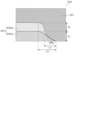
まず、本実施の形態に係る半導体レーザ装置の全体構成について図面を用いて説明する。図1Aは、本実施の形態に係る半導体レーザ装置10の全体構成を示す模式的な平面図である。図1Aにおいては、密着補助層22などの構成を示すために、第二電極23の一部が切り欠かれており、切り欠かれた部分については、輪郭だけが破線で示されている。図1B~図1Fは、本実施の形態に係る半導体レーザ装置10の全体構成を示す模式的な断面図である。図1B~図1Fは、それぞれ、図1Aに示されるIB-IB線、IC-IC線、ID-ID線、IE-IE線及びIF-IF線における断面を示す。


次に、本実施の形態に係る半導体レーザ装置10の主な作用及び効果について、比較例と比較しながら、図1A~図3Bを用いて説明する。
次に、本実施の形態に係る半導体レーザ装置10の製造方法を図4A及び図4Bを用いて説明する。図4Aは、本実施の形態に係る半導体レーザ装置10の製造方法のうち、第一電極25の形成工程までの各工程を示す模式的な断面図である。図4Bは、本実施の形態に係る半導体レーザ装置10の製造方法のうち、密着補助層22の形成工程以降の各工程を示す模式的な断面図である。図4A及び図4Bにおいては、図1Bと同様の位置における断面が示されている。
実施の形態2に係る半導体レーザ装置について説明する。本実施の形態に係る半導体レーザ装置は、主に電流狭窄のための構成において実施の形態1に係る半導体レーザ装置10と相違する。以下、本実施の形態に係る半導体レーザ装置について、実施の形態1に係る半導体レーザ装置10との相違点を中心に図5A及び図5Bを用いて説明する。
実施の形態3に係る半導体レーザ装置について説明する。本実施の形態に係る半導体レーザ装置は、主に絶縁層及び密着補助層の構成において実施の形態1に係る半導体レーザ装置10と相違する。以下、本実施の形態に係る半導体レーザ装置について、実施の形態1に係る半導体レーザ装置10との相違点を中心に図6A~図6Cを用いて説明する。
実施の形態4に係る半導体レーザ装置について説明する。本実施の形態に係る半導体レーザ装置は、主に密着補助層の構成において実施の形態1に係る半導体レーザ装置10と相違する。以下、本実施の形態に係る半導体レーザ装置について、実施の形態1に係る半導体レーザ装置10との相違点を中心に図7A~図7Fを用いて説明する。
実施の形態5に係る半導体レーザ装置について説明する。本実施の形態に係る半導体レーザ装置は、主に第一電極の構成において実施の形態1に係る半導体レーザ装置10と相違する。以下、本実施の形態に係る半導体レーザ装置について、実施の形態1に係る半導体レーザ装置10との相違点を中心に図8A及び図8Bを用いて説明する。
実施の形態6に係る半導体レーザ装置について説明する。本実施の形態に係る半導体レーザ装置は、主に絶縁層の構成において実施の形態1に係る半導体レーザ装置10と相違する。以下、本実施の形態に係る半導体レーザ装置について、実施の形態1に係る半導体レーザ装置10との相違点を中心に図9A及び図9Bを用いて説明する。
実施の形態7に係る半導体レーザ装置について説明する。本実施の形態に係る半導体レーザ装置は、主に、第二電極に接合されるサブマウントを備える点において、実施の形態4に係る半導体レーザ装置310と相違する。以下、本実施の形態に係る半導体レーザ装置について、実施の形態4に係る半導体レーザ装置310との相違点を中心に図10A~図10Cを用いて説明する。
実施の形態8に係る半導体レーザ装置について説明する。本実施の形態に係る半導体レーザ装置は、主に、サブマウントと第二電極との接合構成において、実施の形態7に係る半導体レーザ装置610と相違する。以下、本実施の形態に係る半導体レーザ装置について、実施の形態7に係る半導体レーザ装置610との相違点を中心に図11A~図11Cを用いて説明する。
実施の形態9に係る半導体レーザ装置について説明する。本実施の形態に係る半導体レーザ装置は、主に、第一電極の構成において、実施の形態4に係る半導体レーザ装置310と相違する。以下、本実施の形態に係る半導体レーザ装置について、実施の形態4に係る半導体レーザ装置310との相違点を中心に図12A~図12Cを用いて説明する。
実施の形態10に係る半導体レーザ装置について説明する。本実施の形態に係る半導体レーザ装置は、主に、第一電極の構成において、実施の形態9に係る半導体レーザ装置810と相違する。以下、本実施の形態に係る半導体レーザ装置について、実施の形態9に係る半導体レーザ装置810との相違点を中心に図13A及び図13Bを用いて説明する。
以上、本開示に係る半導体レーザ装置について、各実施の形態に基づいて説明したが、本開示は、上記各実施の形態に限定されるものではない。
12 半田層
13 サブマウント
13a メタル層
13b 基台
15 分離層
17 金属ボール
18 ワイヤ
21、121、221、421、521、1021 絶縁層
22、122、222、322、422、522、1022 密着補助層
23、24、123、223、323、423、523、1023 第二電極
25、125、425、525、825、925、1025 第一電極
26、126、226、326、426、526、1026 第二開口部
27、127、227、427、527、1027 第一開口部
28、1028 n側電極
30、130、1030 半導体積層体
31、1031 基板
32、1032 n型半導体層
33、1033 活性層
34、134、1034 p型半導体層
35、1035 リッジ部
35t 溝部
35w 突出部
36、136、1036 前端面
37、137、1037 後端面
38 側端面
41 酸化膜
42、43、44 感光性レジスト
322a 第一層
322b 第二層
825a、925a 下層電極
825b、925b 上層電極
Claims (21)
- レーザ光を出射する半導体レーザ装置であって、
前記レーザ光を生成する活性層を含む半導体積層体と、
前記半導体積層体の上方に配置された絶縁層と、
前記半導体積層体の上方に配置された第一電極と、
前記第一電極及び前記絶縁層の上方に配置された第二電極と、
前記第二電極と前記絶縁層との間に配置された密着補助層とを備え、
前記半導体積層体は、前記レーザ光の出射端面である前端面と、前記前端面と反対側の面である後端面とを有し、
前記絶縁層は、前記前端面から前記後端面へ向かう第一方向に沿って延びるように形成された第一開口部を有し、
前記密着補助層は、前記密着補助層の平面視において少なくとも一部が前記第一開口部と重なる第二開口部を有し、
前記第一電極の少なくとも一部は、前記密着補助層の平面視において前記第一開口部及び前記第二開口部に配置され、
前記第二電極と前記密着補助層とは、前記前端面及び前記後端面の少なくとも一方の端面と前記第一開口部との間であって、前記絶縁層の上方に配置され、
前記密着補助層の平面視において、前記第二開口部のすべての端縁は、前記第一開口部の端縁の内側、又は、前記第一開口部の端縁上に配置される
半導体レーザ装置。 - 前記第一開口部の端縁は、前記第一電極の外周縁より外側に、前記第一電極から離隔して配置される
請求項1に記載の半導体レーザ装置。 - 前記第一電極の断面の端部は、前記半導体積層体の上面のうち前記第一電極が配置される部分に対して傾斜している
請求項1又は2に記載の半導体レーザ装置。 - 前記第一電極は、下層部と、前記下層部の上方に配置される上層部とを有し、
前記下層部の断面の端部は、前記半導体積層体の上面のうち前記第一電極が配置される部分に対して傾斜しており、かつ、凹状の形状を有する下層凹部を有し、
前記上層部の断面の端部は、前記半導体積層体の上面のうち前記第一電極が配置される部分に対して傾斜しており、かつ、凹状の形状を有する上層凹部を有し、
前記下層凹部は、前記上層凹部より曲率半径が大きい
請求項3に記載の半導体レーザ装置。 - 前記第二電極は、前記第一電極と接する
請求項1~4のいずれか1項に記載の半導体レーザ装置。 - 前記密着補助層の平面視において、前記第二電極の外周縁は、前記密着補助層の外周縁より内側に配置され、かつ、前記第二電極の外周縁は、前記第一開口部の端縁及び前記第二開口部の端縁より外側に配置される
請求項1~5のいずれか1項に記載の半導体レーザ装置。 - 前記第二電極は、前記少なくとも一方の端面に接しない
請求項1~6のいずれか1項に記載の半導体レーザ装置。 - 前記密着補助層は、前記第一電極に接しない
請求項1~7のいずれか1項に記載の半導体レーザ装置。 - 前記半導体積層体は、前記活性層と前記第一電極との間に配置されるp型半導体層を含む
請求項1~8のいずれか1項に記載の半導体レーザ装置。 - 前記半導体積層体は、リッジ部を有し、
前記密着補助層の平面視において、前記リッジ部の上面の少なくとも一部は、前記第一開口部に配置される
請求項1~9のいずれか1項に記載の半導体レーザ装置。 - 前記第二電極は、前記密着補助層より電気伝導度が高い
請求項1~10のいずれか1項に記載の半導体レーザ装置。 - 前記第一電極は、前記密着補助層より、電気伝導度が高い
請求項1~11のいずれか1項に記載の半導体レーザ装置。 - 前記第二電極に接合されるサブマウントをさらに備える
請求項1~12のいずれか1項に記載の半導体レーザ装置。 - 前記第二電極は、Auを含む合金からなる
請求項13に記載の半導体レーザ装置。 - 前記サブマウントは、前記第一方向と交差する端面を備え、
前記密着補助層の平面視において、前記前端面と前記第一開口部との間に、前記端面が配置される
請求項13又は14に記載の半導体レーザ装置。 - 前記第一電極は、オーミック電極である
請求項1~15のいずれか1項に記載の半導体レーザ装置。 - 前記第二電極は、パッド電極である
請求項1~12、16のいずれか1項に記載の半導体レーザ装置。 - 前記第一電極は、Pd、Pt、Ni及びAlの少なくともひとつを含む
請求項1~17のいずれか1項に記載の半導体レーザ装置。 - 前記密着補助層は、Ti及びCrの少なくとも一方を含む
請求項1~18のいずれか1項に記載の半導体レーザ装置。 - 前記第二電極は、Tiを含まない
請求項1~19のいずれか1項に記載の半導体レーザ装置。 - 前記第一電極は、Tiを含まない
請求項1~20のいずれか1項に記載の半導体レーザ装置。
Applications Claiming Priority (3)
| Application Number | Priority Date | Filing Date | Title |
|---|---|---|---|
| JP2018225661 | 2018-11-30 | ||
| JP2018225661 | 2018-11-30 | ||
| PCT/JP2019/044934 WO2020110783A1 (ja) | 2018-11-30 | 2019-11-15 | 半導体レーザ装置 |
Publications (3)
| Publication Number | Publication Date |
|---|---|
| JPWO2020110783A1 JPWO2020110783A1 (ja) | 2021-10-28 |
| JPWO2020110783A5 JPWO2020110783A5 (ja) | 2023-04-04 |
| JP7332623B2 true JP7332623B2 (ja) | 2023-08-23 |
Family
ID=70852964
Family Applications (1)
| Application Number | Title | Priority Date | Filing Date |
|---|---|---|---|
| JP2020558355A Active JP7332623B2 (ja) | 2018-11-30 | 2019-11-15 | 半導体レーザ装置 |
Country Status (3)
| Country | Link |
|---|---|
| US (1) | US12142895B2 (ja) |
| JP (1) | JP7332623B2 (ja) |
| WO (1) | WO2020110783A1 (ja) |
Families Citing this family (4)
| Publication number | Priority date | Publication date | Assignee | Title |
|---|---|---|---|---|
| JP2022020503A (ja) | 2020-07-20 | 2022-02-01 | ソニーグループ株式会社 | 半導体レーザおよび半導体レーザ装置 |
| WO2022158557A1 (ja) * | 2021-01-22 | 2022-07-28 | 京セラ株式会社 | 発光素子、半導体レーザ素子並びにその製造方法および製造装置 |
| CN118715679A (zh) * | 2022-02-22 | 2024-09-27 | 新唐科技日本株式会社 | 半导体激光元件及半导体激光元件的制造方法 |
| JPWO2023223859A1 (ja) * | 2022-05-19 | 2023-11-23 |
Citations (6)
| Publication number | Priority date | Publication date | Assignee | Title |
|---|---|---|---|---|
| JP2005109291A (ja) | 2003-10-01 | 2005-04-21 | Nichia Chem Ind Ltd | 半導体レーザ素子 |
| JP2010062300A (ja) | 2008-09-03 | 2010-03-18 | Rohm Co Ltd | 窒化物半導体素子およびその製造方法 |
| JP2011135016A (ja) | 2009-12-25 | 2011-07-07 | Sumitomo Electric Ind Ltd | Iii族窒化物半導体レーザ素子、及びiii族窒化物半導体レーザ素子を作製する方法 |
| JP2013125886A (ja) | 2011-12-15 | 2013-06-24 | Sony Corp | 半導体レーザ素子及び半導体レーザ素子の製造方法 |
| US20170054271A1 (en) | 2014-04-11 | 2017-02-23 | Osram Opto Semiconductors Gmbh | Semiconductor Strip Laser and Semiconductor Component |
| WO2018180524A1 (ja) | 2017-03-28 | 2018-10-04 | パナソニック株式会社 | 窒化物半導体レーザ素子および窒化物半導体レーザ装置 |
Family Cites Families (6)
| Publication number | Priority date | Publication date | Assignee | Title |
|---|---|---|---|---|
| JP2006013331A (ja) | 2004-06-29 | 2006-01-12 | Sanyo Electric Co Ltd | 半導体レーザ素子 |
| JP2007027572A (ja) * | 2005-07-20 | 2007-02-01 | Sony Corp | 半導体発光装置およびその製造方法 |
| JP4948307B2 (ja) * | 2006-07-31 | 2012-06-06 | 三洋電機株式会社 | 半導体レーザ素子およびその製造方法 |
| JP5100407B2 (ja) | 2008-01-17 | 2012-12-19 | シャープ株式会社 | 半導体発光素子およびそれを用いた半導体発光装置 |
| JP2011165869A (ja) * | 2010-02-09 | 2011-08-25 | Mitsubishi Electric Corp | 半導体発光素子及びその製造方法 |
| JP2020077715A (ja) * | 2018-11-06 | 2020-05-21 | 富士通株式会社 | 光モジュール、光通信機器および製造方法 |
-
2019
- 2019-11-15 JP JP2020558355A patent/JP7332623B2/ja active Active
- 2019-11-15 WO PCT/JP2019/044934 patent/WO2020110783A1/ja not_active Ceased
-
2021
- 2021-05-26 US US17/331,128 patent/US12142895B2/en active Active
Patent Citations (6)
| Publication number | Priority date | Publication date | Assignee | Title |
|---|---|---|---|---|
| JP2005109291A (ja) | 2003-10-01 | 2005-04-21 | Nichia Chem Ind Ltd | 半導体レーザ素子 |
| JP2010062300A (ja) | 2008-09-03 | 2010-03-18 | Rohm Co Ltd | 窒化物半導体素子およびその製造方法 |
| JP2011135016A (ja) | 2009-12-25 | 2011-07-07 | Sumitomo Electric Ind Ltd | Iii族窒化物半導体レーザ素子、及びiii族窒化物半導体レーザ素子を作製する方法 |
| JP2013125886A (ja) | 2011-12-15 | 2013-06-24 | Sony Corp | 半導体レーザ素子及び半導体レーザ素子の製造方法 |
| US20170054271A1 (en) | 2014-04-11 | 2017-02-23 | Osram Opto Semiconductors Gmbh | Semiconductor Strip Laser and Semiconductor Component |
| WO2018180524A1 (ja) | 2017-03-28 | 2018-10-04 | パナソニック株式会社 | 窒化物半導体レーザ素子および窒化物半導体レーザ装置 |
Also Published As
| Publication number | Publication date |
|---|---|
| US20210281038A1 (en) | 2021-09-09 |
| US12142895B2 (en) | 2024-11-12 |
| WO2020110783A1 (ja) | 2020-06-04 |
| JPWO2020110783A1 (ja) | 2021-10-28 |
Similar Documents
| Publication | Publication Date | Title |
|---|---|---|
| JP7191167B2 (ja) | 半導体レーザーダイオード | |
| JP4352337B2 (ja) | 半導体レーザおよび半導体レーザ装置 | |
| US12142895B2 (en) | Semiconductor laser device | |
| US12483006B2 (en) | Edge-emitting laser bar | |
| CN102904156A (zh) | 半导体激光器元件及其制造方法 | |
| US20070274360A1 (en) | Semiconductor laser element and semiconductor laser device | |
| JP2007081399A (ja) | キャビティ内コンタクトのための高融点金属ELOGマスクを備えているGaNレーザ | |
| JP2012094564A (ja) | 半導体レーザ素子およびその製造方法 | |
| JP2009099959A (ja) | 窒化物系半導体レーザ素子 | |
| JP4697488B2 (ja) | マルチビーム半導体レーザ | |
| JP5127642B2 (ja) | 窒化物系半導体レーザ素子 | |
| JP5103008B2 (ja) | 半導体レーザ素子及び半導体レーザ装置 | |
| JP2007027572A (ja) | 半導体発光装置およびその製造方法 | |
| JP7391944B2 (ja) | 半導体レーザ素子 | |
| US20230335972A1 (en) | Semiconductor laser and semiconductor laser device | |
| JP6140101B2 (ja) | 半導体光装置 | |
| JP2011258883A (ja) | 半導体レーザ | |
| JPH11340570A (ja) | 光電変換素子およびその製造方法 | |
| JP4737387B2 (ja) | 半導体レーザ素子 | |
| US20240162686A1 (en) | Semiconductor laser | |
| JP7774456B2 (ja) | 半導体レーザ装置 | |
| JP2007158008A (ja) | 半導体発光素子 |
Legal Events
| Date | Code | Title | Description |
|---|---|---|---|
| A521 | Request for written amendment filed |
Free format text: JAPANESE INTERMEDIATE CODE: A523 Effective date: 20210528 |
|
| A621 | Written request for application examination |
Free format text: JAPANESE INTERMEDIATE CODE: A621 Effective date: 20221111 |
|
| A521 | Request for written amendment filed |
Free format text: JAPANESE INTERMEDIATE CODE: A523 Effective date: 20230327 |
|
| TRDD | Decision of grant or rejection written | ||
| A01 | Written decision to grant a patent or to grant a registration (utility model) |
Free format text: JAPANESE INTERMEDIATE CODE: A01 Effective date: 20230718 |
|
| A61 | First payment of annual fees (during grant procedure) |
Free format text: JAPANESE INTERMEDIATE CODE: A61 Effective date: 20230810 |
|
| R150 | Certificate of patent or registration of utility model |
Ref document number: 7332623 Country of ref document: JP Free format text: JAPANESE INTERMEDIATE CODE: R150 |