JP7404371B2 - 複数の格子を形成する方法 - Google Patents
複数の格子を形成する方法 Download PDFInfo
- Publication number
- JP7404371B2 JP7404371B2 JP2021533803A JP2021533803A JP7404371B2 JP 7404371 B2 JP7404371 B2 JP 7404371B2 JP 2021533803 A JP2021533803 A JP 2021533803A JP 2021533803 A JP2021533803 A JP 2021533803A JP 7404371 B2 JP7404371 B2 JP 7404371B2
- Authority
- JP
- Japan
- Prior art keywords
- gratings
- grating
- protective material
- thickness
- depositing
- Prior art date
- Legal status (The legal status is an assumption and is not a legal conclusion. Google has not performed a legal analysis and makes no representation as to the accuracy of the status listed.)
- Active
Links
Images




Classifications
-
- G—PHYSICS
- G02—OPTICS
- G02B—OPTICAL ELEMENTS, SYSTEMS OR APPARATUS
- G02B6/00—Light guides; Structural details of arrangements comprising light guides and other optical elements, e.g. couplings
- G02B6/0001—Light guides; Structural details of arrangements comprising light guides and other optical elements, e.g. couplings specially adapted for lighting devices or systems
- G02B6/0011—Light guides; Structural details of arrangements comprising light guides and other optical elements, e.g. couplings specially adapted for lighting devices or systems the light guides being planar or of plate-like form
- G02B6/0065—Manufacturing aspects; Material aspects
-
- B—PERFORMING OPERATIONS; TRANSPORTING
- B23—MACHINE TOOLS; METAL-WORKING NOT OTHERWISE PROVIDED FOR
- B23K—SOLDERING OR UNSOLDERING; WELDING; CLADDING OR PLATING BY SOLDERING OR WELDING; CUTTING BY APPLYING HEAT LOCALLY, e.g. FLAME CUTTING; WORKING BY LASER BEAM
- B23K26/00—Working by laser beam, e.g. welding, cutting or boring
- B23K26/34—Laser welding for purposes other than joining
-
- H—ELECTRICITY
- H10—SEMICONDUCTOR DEVICES; ELECTRIC SOLID-STATE DEVICES NOT OTHERWISE PROVIDED FOR
- H10P—GENERIC PROCESSES OR APPARATUS FOR THE MANUFACTURE OR TREATMENT OF DEVICES COVERED BY CLASS H10
- H10P72/00—Handling or holding of wafers, substrates or devices during manufacture or treatment thereof
- H10P72/06—Apparatus for monitoring, sorting, marking, testing or measuring
- H10P72/0602—Temperature monitoring
-
- B—PERFORMING OPERATIONS; TRANSPORTING
- B23—MACHINE TOOLS; METAL-WORKING NOT OTHERWISE PROVIDED FOR
- B23K—SOLDERING OR UNSOLDERING; WELDING; CLADDING OR PLATING BY SOLDERING OR WELDING; CUTTING BY APPLYING HEAT LOCALLY, e.g. FLAME CUTTING; WORKING BY LASER BEAM
- B23K26/00—Working by laser beam, e.g. welding, cutting or boring
- B23K26/36—Removing material
- B23K26/362—Laser etching
- B23K26/364—Laser etching for making a groove or trench, e.g. for scribing a break initiation groove
-
- B—PERFORMING OPERATIONS; TRANSPORTING
- B29—WORKING OF PLASTICS; WORKING OF SUBSTANCES IN A PLASTIC STATE IN GENERAL
- B29D—PRODUCING PARTICULAR ARTICLES FROM PLASTICS OR FROM SUBSTANCES IN A PLASTIC STATE
- B29D11/00—Producing optical elements, e.g. lenses or prisms
- B29D11/0074—Production of other optical elements not provided for in B29D11/00009- B29D11/0073
- B29D11/00769—Producing diffraction gratings
-
- C—CHEMISTRY; METALLURGY
- C04—CEMENTS; CONCRETE; ARTIFICIAL STONE; CERAMICS; REFRACTORIES
- C04B—LIME, MAGNESIA; SLAG; CEMENTS; COMPOSITIONS THEREOF, e.g. MORTARS, CONCRETE OR LIKE BUILDING MATERIALS; ARTIFICIAL STONE; CERAMICS; REFRACTORIES; TREATMENT OF NATURAL STONE
- C04B41/00—After-treatment of mortars, concrete, artificial stone or ceramics; Treatment of natural stone
- C04B41/0036—Laser treatment
-
- G—PHYSICS
- G02—OPTICS
- G02B—OPTICAL ELEMENTS, SYSTEMS OR APPARATUS
- G02B27/00—Optical systems or apparatus not provided for by any of the groups G02B1/00 - G02B26/00, G02B30/00
- G02B27/01—Head-up displays
- G02B27/017—Head mounted
- G02B27/0172—Head mounted characterised by optical features
-
- G—PHYSICS
- G02—OPTICS
- G02B—OPTICAL ELEMENTS, SYSTEMS OR APPARATUS
- G02B27/00—Optical systems or apparatus not provided for by any of the groups G02B1/00 - G02B26/00, G02B30/00
- G02B27/42—Diffraction optics, i.e. systems including a diffractive element being designed for providing a diffractive effect
- G02B27/4272—Diffraction optics, i.e. systems including a diffractive element being designed for providing a diffractive effect having plural diffractive elements positioned sequentially along the optical path
-
- G—PHYSICS
- G02—OPTICS
- G02B—OPTICAL ELEMENTS, SYSTEMS OR APPARATUS
- G02B5/00—Optical elements other than lenses
- G02B5/18—Diffraction gratings
- G02B5/1814—Diffraction gratings structurally combined with one or more further optical elements, e.g. lenses, mirrors, prisms or other diffraction gratings
- G02B5/1819—Plural gratings positioned on the same surface, e.g. array of gratings
-
- G—PHYSICS
- G02—OPTICS
- G02B—OPTICAL ELEMENTS, SYSTEMS OR APPARATUS
- G02B5/00—Optical elements other than lenses
- G02B5/18—Diffraction gratings
- G02B5/1847—Manufacturing methods
- G02B5/1857—Manufacturing methods using exposure or etching means, e.g. holography, photolithography, exposure to electron or ion beams
-
- G—PHYSICS
- G02—OPTICS
- G02B—OPTICAL ELEMENTS, SYSTEMS OR APPARATUS
- G02B6/00—Light guides; Structural details of arrangements comprising light guides and other optical elements, e.g. couplings
- G02B6/24—Coupling light guides
- G02B6/26—Optical coupling means
- G02B6/34—Optical coupling means utilising prism or grating
-
- G—PHYSICS
- G03—PHOTOGRAPHY; CINEMATOGRAPHY; ANALOGOUS TECHNIQUES USING WAVES OTHER THAN OPTICAL WAVES; ELECTROGRAPHY; HOLOGRAPHY
- G03F—PHOTOMECHANICAL PRODUCTION OF TEXTURED OR PATTERNED SURFACES, e.g. FOR PRINTING, FOR PROCESSING OF SEMICONDUCTOR DEVICES; MATERIALS THEREFOR; ORIGINALS THEREFOR; APPARATUS SPECIALLY ADAPTED THEREFOR
- G03F7/00—Photomechanical, e.g. photolithographic, production of textured or patterned surfaces, e.g. printing surfaces; Materials therefor, e.g. comprising photoresists; Apparatus specially adapted therefor
- G03F7/0005—Production of optical devices or components in so far as characterised by the lithographic processes or materials used therefor
-
- G—PHYSICS
- G06—COMPUTING OR CALCULATING; COUNTING
- G06F—ELECTRIC DIGITAL DATA PROCESSING
- G06F3/00—Input arrangements for transferring data to be processed into a form capable of being handled by the computer; Output arrangements for transferring data from processing unit to output unit, e.g. interface arrangements
- G06F3/01—Input arrangements or combined input and output arrangements for interaction between user and computer
- G06F3/011—Arrangements for interaction with the human body, e.g. for user immersion in virtual reality
-
- H—ELECTRICITY
- H10—SEMICONDUCTOR DEVICES; ELECTRIC SOLID-STATE DEVICES NOT OTHERWISE PROVIDED FOR
- H10H—INORGANIC LIGHT-EMITTING SEMICONDUCTOR DEVICES HAVING POTENTIAL BARRIERS
- H10H29/00—Integrated devices, or assemblies of multiple devices, comprising at least one light-emitting semiconductor element covered by group H10H20/00
- H10H29/10—Integrated devices comprising at least one light-emitting semiconductor component covered by group H10H20/00
- H10H29/14—Integrated devices comprising at least one light-emitting semiconductor component covered by group H10H20/00 comprising multiple light-emitting semiconductor components
- H10H29/142—Two-dimensional arrangements, e.g. asymmetric LED layout
-
- H—ELECTRICITY
- H10—SEMICONDUCTOR DEVICES; ELECTRIC SOLID-STATE DEVICES NOT OTHERWISE PROVIDED FOR
- H10P—GENERIC PROCESSES OR APPARATUS FOR THE MANUFACTURE OR TREATMENT OF DEVICES COVERED BY CLASS H10
- H10P30/00—Ion implantation into wafers, substrates or parts of devices
- H10P30/20—Ion implantation into wafers, substrates or parts of devices into semiconductor materials, e.g. for doping
- H10P30/202—Ion implantation into wafers, substrates or parts of devices into semiconductor materials, e.g. for doping characterised by the semiconductor materials
-
- H—ELECTRICITY
- H10—SEMICONDUCTOR DEVICES; ELECTRIC SOLID-STATE DEVICES NOT OTHERWISE PROVIDED FOR
- H10P—GENERIC PROCESSES OR APPARATUS FOR THE MANUFACTURE OR TREATMENT OF DEVICES COVERED BY CLASS H10
- H10P50/00—Etching of wafers, substrates or parts of devices
-
- H—ELECTRICITY
- H10—SEMICONDUCTOR DEVICES; ELECTRIC SOLID-STATE DEVICES NOT OTHERWISE PROVIDED FOR
- H10P—GENERIC PROCESSES OR APPARATUS FOR THE MANUFACTURE OR TREATMENT OF DEVICES COVERED BY CLASS H10
- H10P76/00—Manufacture or treatment of masks on semiconductor bodies, e.g. by lithography or photolithography
- H10P76/20—Manufacture or treatment of masks on semiconductor bodies, e.g. by lithography or photolithography of masks comprising organic materials
- H10P76/204—Manufacture or treatment of masks on semiconductor bodies, e.g. by lithography or photolithography of masks comprising organic materials of organic photoresist masks
- H10P76/2049—Ion beam lithography processes
-
- H—ELECTRICITY
- H10—SEMICONDUCTOR DEVICES; ELECTRIC SOLID-STATE DEVICES NOT OTHERWISE PROVIDED FOR
- H10W—GENERIC PACKAGES, INTERCONNECTIONS, CONNECTORS OR OTHER CONSTRUCTIONAL DETAILS OF DEVICES COVERED BY CLASS H10
- H10W90/00—Package configurations
-
- G—PHYSICS
- G02—OPTICS
- G02B—OPTICAL ELEMENTS, SYSTEMS OR APPARATUS
- G02B6/00—Light guides; Structural details of arrangements comprising light guides and other optical elements, e.g. couplings
- G02B6/0001—Light guides; Structural details of arrangements comprising light guides and other optical elements, e.g. couplings specially adapted for lighting devices or systems
- G02B6/0011—Light guides; Structural details of arrangements comprising light guides and other optical elements, e.g. couplings specially adapted for lighting devices or systems the light guides being planar or of plate-like form
- G02B6/0013—Means for improving the coupling-in of light from the light source into the light guide
- G02B6/0015—Means for improving the coupling-in of light from the light source into the light guide provided on the surface of the light guide or in the bulk of it
- G02B6/0016—Grooves, prisms, gratings, scattering particles or rough surfaces
Landscapes
- Physics & Mathematics (AREA)
- Engineering & Computer Science (AREA)
- Optics & Photonics (AREA)
- General Physics & Mathematics (AREA)
- Manufacturing & Machinery (AREA)
- Chemical & Material Sciences (AREA)
- Mechanical Engineering (AREA)
- Ceramic Engineering (AREA)
- Plasma & Fusion (AREA)
- General Engineering & Computer Science (AREA)
- Theoretical Computer Science (AREA)
- Materials Engineering (AREA)
- Organic Chemistry (AREA)
- Structural Engineering (AREA)
- Human Computer Interaction (AREA)
- Health & Medical Sciences (AREA)
- Ophthalmology & Optometry (AREA)
- Optical Integrated Circuits (AREA)
- Drying Of Semiconductors (AREA)
- Diffracting Gratings Or Hologram Optical Elements (AREA)
- Optical Modulation, Optical Deflection, Nonlinear Optics, Optical Demodulation, Optical Logic Elements (AREA)
- Microelectronics & Electronic Packaging (AREA)
- Recrystallisation Techniques (AREA)
- Led Devices (AREA)
- Container, Conveyance, Adherence, Positioning, Of Wafer (AREA)
Description
本出願の実施形態は方法に関し、より具体的には、複数の格子を形成する方法に関する。
仮想現実とは、一般に、コンピュータで生成された模擬環境であって、その中でユーザが見かけ上の物理的存在を有する、模擬環境であると考えられる。仮想現実体験は、三次元(3D)で生成されることが可能であり、実際の環境を置換する仮想現実環境を表示するためのレンズとしてニアアイディスプレイパネルを有する、眼鏡又はその他のウエアラブルディスプレイデバイスといったヘッドマウントディスプレイ(HMD)を用いて視認されうる。
Claims (15)
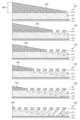
- 第1の複数の格子を形成する方法であって、
基板上に配置された格子材料の上に保護材料を堆積させることであって、前記保護材料が、前記格子材料上に配置されたパターニングされたハードマスクの部分間に堆積され、前記保護材料は、前記格子材料の平坦な上面から前記保護材料の上面までの厚さを有し、前記保護材料の前記厚さは、イオンビームが前記格子材料に向けて方向付けられた時に前記保護材料の前記厚さが前記格子材料の除去を少なくとも部分的に阻害するように、前記格子材料の平坦な上面に沿って変動する、保護材料を堆積させることと、
前記格子材料の少なくとも一部分が除去され、これにより前記保護材料の前記厚さにそれぞれ対応する深さプロファイルを有する前記第1の複数の格子が形成されて、前記第1の複数の格子のうちの少なくとも1つの格子が前記第1の複数の格子のうちの他の格子とは異なる厚さを有するように、前記イオンビームを前記格子材料に向けて方向付けることと、を含み、前記第1の複数の格子のうちの少なくとも1つの格子が、5°~85°の角度を有する、
方法。 - 前記保護材料を堆積させることは、前記格子材料の第1部分と第2部分の上に前記保護材料を堆積させることであって、これにより、前記厚さを有する前記保護材料が、前記第1部分における前記格子材料の除去を完全に阻害する、前記保護材料を堆積させることと、
前記第2部分の上の前記保護材料を除去することと、を含む、請求項1に記載の方法。 - 前記第1部分の上に配置された前記保護材料が、前記第2部分の上に配置された前記保護材料よりも厚い、請求項2に記載の方法。
- 前記保護材料の前記厚さが、前記第1の複数の格子にわたって2次元的に変動するか、又は前記格子材料にわたって線形に変動する、請求項1に記載の方法。
- 複数の格子を形成する方法であって、
基板上に配置された格子材料の第1部分の上に保護材料を堆積させることであって、前記格子材料の前記第1部分は第2部分に隣接しており、前記保護材料が、前記第1部分上のパターニングされたハードマスクの部分間に配置され、前記パターニングされたハードマスクは、前記格子材料の上に配置され、前記保護材料は、前記格子材料の平坦な上面から前記保護材料の上面までの厚さを含み、前記保護材料の前記厚さは、イオンビームが前記格子材料に向けて方向付けられた時に前記格子材料の前記第1部分の除去を阻害する、保護材料を堆積させることと、
前記複数の格子が形成されるように、前記イオンビームを前記格子材料の前記第1部分及び前記第2部分に向けて方向付けることであって、前記第1部分において第1の複数の格子が形成され、前記第2部分において第2の複数の格子が形成され、前記第1の複数の格子は前記第2の複数の格子の第2の深さよりも小さな第1の深さを有し、前記第1の深さは対応する前記保護材料の厚さに基づく、前記イオンビームを前記格子材料の前記第1部分及び前記第2部分に向けて方向付けることと、を含み、
前記第1の複数の格子及び前記第2の複数の格子のうちの少なくとも1つの格子が、5°~85°の角度を有する、
方法。 - 前記格子材料の前記第2部分の上に前記保護材料を堆積させることを更に含む、請求項5に記載の方法。
- 前記第1部分の上に配置された前記保護材料が、前記第2部分の上に配置された前記保護材料よりも厚い、請求項6に記載の方法。
- 前記第1の複数の格子のうちの少なくとも1つの格子が、前記第1の複数の格子のうちの他の格子とは異なる厚さを有する、請求項5に記載の方法。
- 前記保護材料を堆積させること及び前記イオンビームを方向付けることが反復される、請求項5に記載の方法。
- 第1の複数の格子を形成する方法であって、:
基板上に配置された格子材料の第1部分及び第2部分の上に保護材料を堆積させることであって、前記格子材料の前記第1部分は第2部分に隣接しており、前記保護材料が、前記第1部分及び前記第2部分上のパターニングされたハードマスクの部分間に配置され、前記パターニングされたハードマスクは、前記格子材料の上に配置され、前記保護材料は、
前記格子材料の平坦な上面から前記保護材料の上面までの第1の厚さであって、イオンビームが前記第1部分に向けて方向付けられた時に前記格子材料の前記第1部分の除去を阻害する、前記保護材料の前記第1の厚さと、
前記格子材料の平坦な上面から前記保護材料の上面までの第2の厚さであって、イオンビームが前記第2部分に向けて方向付けられた時に前記格子材料の前記第2部分の除去を阻害する前記第2の厚さと、を含む、保護材料を堆積させることと、
前記第1の複数の格子及び第2の複数の格子が形成されるように、前記イオンビームを前記格子材料の前記第1部分及び前記第2部分に向けて方向付けることであって、前記第1部分において前記第1の複数の格子が形成され、前記第2部分において前記第2の複数の格子が形成され、前記第1の複数の格子は前記第2の複数の格子の第2の深さよりも小さな第1の深さを有し、前記第1の複数の格子の前記第1の深さは前記保護材料の前記第1の厚さに基づき、前記第2の複数の格子の前記第2の深さは前記保護材料の前記第2の厚さに基づく、前記イオンビームを前記格子材料の前記第1部分及び前記第2部分に向けて方向付けることと、を含み、
前記第1の複数の格子及び前記第2の複数の格子のうちの少なくとも1つの格子は、5°~85°の角度を有し、
前記第2部分の上に前記保護材料を堆積させることが、複数の加熱ピクセル又は発光ダイオード(LED)に前記保護材料を曝露することを含む、
方法。 - 前記複数の加熱ピクセル又はLEDの各々が個別に制御される、請求項10に記載の方法。
- 前記基板の裏面に、前記第1部分に対応する温度分布が提供される、請求項11に記載の方法。
- 前記第1の複数の格子のうちの少なくとも1つの格子が、前記第1の複数の格子のうちの他の格子とは異なる厚さを有する、請求項10に記載の方法。
- 前記保護材料がジアゾナフトキノン、フェノールホルムアルデヒド樹脂、ポリ(メチルメタクリレート)、ポリ(メチルグルタルイミド)、及びSU-8の少なくとも1つを含む、請求項10に記載の方法。
- 前記保護材料を堆積させることが、インクジェットプリンティング又は三次元(3D)プリンティングを含む、請求項10に記載の方法。
Priority Applications (1)
| Application Number | Priority Date | Filing Date | Title |
|---|---|---|---|
| JP2023209912A JP7663668B2 (ja) | 2018-12-17 | 2023-12-13 | 複数の格子を形成する方法 |
Applications Claiming Priority (3)
| Application Number | Priority Date | Filing Date | Title |
|---|---|---|---|
| US201862780802P | 2018-12-17 | 2018-12-17 | |
| US62/780,802 | 2018-12-17 | ||
| PCT/US2019/066812 WO2020131852A1 (en) | 2018-12-17 | 2019-12-17 | Method of forming a plurality of gratings |
Related Child Applications (1)
| Application Number | Title | Priority Date | Filing Date |
|---|---|---|---|
| JP2023209912A Division JP7663668B2 (ja) | 2018-12-17 | 2023-12-13 | 複数の格子を形成する方法 |
Publications (2)
| Publication Number | Publication Date |
|---|---|
| JP2022514525A JP2022514525A (ja) | 2022-02-14 |
| JP7404371B2 true JP7404371B2 (ja) | 2023-12-25 |
Family
ID=71072279
Family Applications (3)
| Application Number | Title | Priority Date | Filing Date |
|---|---|---|---|
| JP2021533802A Pending JP2022514524A (ja) | 2018-12-17 | 2019-11-25 | 局所加熱によるエッチング深さの制御方法 |
| JP2021533803A Active JP7404371B2 (ja) | 2018-12-17 | 2019-12-17 | 複数の格子を形成する方法 |
| JP2023209912A Active JP7663668B2 (ja) | 2018-12-17 | 2023-12-13 | 複数の格子を形成する方法 |
Family Applications Before (1)
| Application Number | Title | Priority Date | Filing Date |
|---|---|---|---|
| JP2021533802A Pending JP2022514524A (ja) | 2018-12-17 | 2019-11-25 | 局所加熱によるエッチング深さの制御方法 |
Family Applications After (1)
| Application Number | Title | Priority Date | Filing Date |
|---|---|---|---|
| JP2023209912A Active JP7663668B2 (ja) | 2018-12-17 | 2023-12-13 | 複数の格子を形成する方法 |
Country Status (7)
| Country | Link |
|---|---|
| US (3) | US11554445B2 (ja) |
| EP (2) | EP3900027B1 (ja) |
| JP (3) | JP2022514524A (ja) |
| KR (2) | KR102871301B1 (ja) |
| CN (2) | CN113169099B (ja) |
| TW (3) | TWI801948B (ja) |
| WO (2) | WO2020131317A1 (ja) |
Families Citing this family (12)
| Publication number | Priority date | Publication date | Assignee | Title |
|---|---|---|---|---|
| WO2020131317A1 (en) * | 2018-12-17 | 2020-06-25 | Applied Materials, Inc. | Methods for controlling etch depth by localized heating |
| US20220171105A1 (en) * | 2020-09-11 | 2022-06-02 | Board Of Regents, The University Of Texas System | Resonant filters having simultaneously tuned central wavelengths and sidebands |
| US20220082739A1 (en) * | 2020-09-17 | 2022-03-17 | Facebook Technologies, Llc | Techniques for manufacturing variable etch depth gratings using gray-tone lithography |
| FI130396B (fi) * | 2020-09-23 | 2023-08-10 | Dispelix Oy | Optinen aaltojohde lisätyn todellisuuden näyttölaitteeseen |
| WO2022066941A1 (en) * | 2020-09-23 | 2022-03-31 | Applied Materials, Inc. | Fabrication of diffractive optic element having a variable refractive index profile by inkjet printing deposition |
| CN116635787A (zh) | 2020-11-30 | 2023-08-22 | 应用材料公司 | 用以形成具倾斜角的结构的平版印刷术方法 |
| US12259552B2 (en) * | 2020-12-17 | 2025-03-25 | Google Llc | Spatial variance along waveguide incoupler |
| CN112684536B (zh) * | 2021-03-19 | 2021-06-04 | 北京至格科技有限公司 | 一种光波导器件及近眼显示设备 |
| FI130664B1 (fi) * | 2021-05-17 | 2024-01-09 | Dispelix Oy | Menetelmä porrastetun hilan valmistamiseksi |
| CN114273785B (zh) * | 2021-12-14 | 2025-02-18 | 莆田市鑫镭腾科技有限公司 | 一种光纤激光器流水线二维码打标方法及系统 |
| US11892676B2 (en) * | 2022-01-10 | 2024-02-06 | Applied Materials, Inc. | Self-aligned formation of angled optical device structures |
| CN116564800B (zh) * | 2023-07-04 | 2023-09-08 | 芯众享(成都)微电子有限公司 | 一种在半导体表面一次形成具有不同深度沟槽的方法 |
Citations (6)
| Publication number | Priority date | Publication date | Assignee | Title |
|---|---|---|---|---|
| JP2003100706A (ja) | 2001-09-26 | 2003-04-04 | Shin Etsu Handotai Co Ltd | ドライエッチング方法 |
| US20070263973A1 (en) | 2006-05-12 | 2007-11-15 | Interuniversitair Microelektronica Centrum (Imec) | Slanted Segmented Coupler |
| JP2011237374A (ja) | 2010-05-13 | 2011-11-24 | Seiko Epson Corp | 分光装置、検出装置及び分光装置の製造方法 |
| CN103675969A (zh) | 2013-12-04 | 2014-03-26 | 中国科学院上海光学精密机械研究所 | 高效率斜双层光栅 |
| JP2016177244A (ja) | 2015-03-18 | 2016-10-06 | エーエスエムエル ネザーランズ ビー.ブイ. | リソグラフィ装置における加熱システムおよび冷却システム |
| JP2022506595A (ja) | 2018-11-07 | 2022-01-17 | アプライド マテリアルズ インコーポレイテッド | グレートーンリソグラフィと傾斜エッチングを使用した、深さ調節された傾斜格子 |
Family Cites Families (37)
| Publication number | Priority date | Publication date | Assignee | Title |
|---|---|---|---|---|
| JPH0653600A (ja) | 1992-07-30 | 1994-02-25 | Oki Electric Ind Co Ltd | 半導体発光素子の回折格子の形成方法 |
| JPH0669605A (ja) * | 1992-08-21 | 1994-03-11 | Oki Electric Ind Co Ltd | 回折格子の形成方法 |
| JPH06201909A (ja) | 1992-12-28 | 1994-07-22 | Canon Inc | 回折格子の製造方法 |
| JPH0829606A (ja) * | 1994-07-11 | 1996-02-02 | Canon Inc | 位相シフト回折格子の作製方法 |
| JP2002189112A (ja) * | 2000-12-22 | 2002-07-05 | Canon Inc | 回折光学素子の製造方法、回折光学素子の製造方法によって製造したことを特徴とする回折光学素子製造用金型、回折光学素子、および該回折光学素子を有する光学系、光学機器、露光装置、デバイス製造方法、デバイス |
| US7435193B2 (en) | 2005-07-28 | 2008-10-14 | Johnson Larry W | Retrieval device for tethered articles |
| US7569463B2 (en) * | 2006-03-08 | 2009-08-04 | Applied Materials, Inc. | Method of thermal processing structures formed on a substrate |
| US20090120924A1 (en) | 2007-11-08 | 2009-05-14 | Stephen Moffatt | Pulse train annealing method and apparatus |
| US20100304061A1 (en) | 2009-05-26 | 2010-12-02 | Zena Technologies, Inc. | Fabrication of high aspect ratio features in a glass layer by etching |
| US8247332B2 (en) * | 2009-12-04 | 2012-08-21 | Novellus Systems, Inc. | Hardmask materials |
| JP5786487B2 (ja) * | 2011-06-22 | 2015-09-30 | 東京エレクトロン株式会社 | 熱処理装置及び熱処理方法 |
| KR101905158B1 (ko) * | 2013-08-06 | 2018-10-08 | 어플라이드 머티어리얼스, 인코포레이티드 | 국부적으로 가열되는 다-구역 기판 지지부 |
| US9472410B2 (en) * | 2014-03-05 | 2016-10-18 | Applied Materials, Inc. | Pixelated capacitance controlled ESC |
| WO2015173686A1 (en) * | 2014-05-16 | 2015-11-19 | Semiconductor Energy Laboratory Co., Ltd. | Electronic device with secondary battery |
| US20160033784A1 (en) * | 2014-07-30 | 2016-02-04 | Tapani Levola | Optical Components |
| US20160035539A1 (en) * | 2014-07-30 | 2016-02-04 | Lauri SAINIEMI | Microfabrication |
| US9287148B1 (en) * | 2014-12-18 | 2016-03-15 | Varian Semiconductor Equipment Associates, Inc. | Dynamic heating method and system for wafer processing |
| US9685303B2 (en) | 2015-05-08 | 2017-06-20 | Varian Semiconductor Equipment Associates, Inc. | Apparatus for heating and processing a substrate |
| KR20180011119A (ko) * | 2015-05-22 | 2018-01-31 | 어플라이드 머티어리얼스, 인코포레이티드 | 방위방향으로 튜닝가능한 다중-구역 정전 척 |
| US9910276B2 (en) | 2015-06-30 | 2018-03-06 | Microsoft Technology Licensing, Llc | Diffractive optical elements with graded edges |
| WO2017210178A1 (en) * | 2016-06-02 | 2017-12-07 | Axcelis Technologies, Inc. | Apparatus and method for heating or cooling a wafer |
| WO2018039273A1 (en) | 2016-08-22 | 2018-03-01 | Magic Leap, Inc. | Dithering methods and apparatus for wearable display device |
| US10436958B2 (en) | 2016-10-05 | 2019-10-08 | Magic Leap, Inc. | Fabricating non-uniform diffraction gratings |
| AU2018235893A1 (en) * | 2017-03-15 | 2019-10-31 | Callaghan Innovation | Apparatus for and method of manufacturing an article using photolithography and a photoresist |
| FI128629B (en) * | 2017-06-02 | 2020-09-15 | Dispelix Oy | Method for making a master plate and a master plate |
| US10684407B2 (en) * | 2017-10-30 | 2020-06-16 | Facebook Technologies, Llc | Reactivity enhancement in ion beam etcher |
| EP3717967A4 (en) | 2017-11-29 | 2021-09-01 | Applied Materials, Inc. | METHOD OF MANUFACTURING WAVE CONDUCTOR COMBINATORS USING DIRECT ETCHES |
| US10598832B2 (en) | 2018-01-09 | 2020-03-24 | Varian Semiconductor Equipment Associates, Inc. | System and method for forming diffracted optical element having varied gratings |
| US10818499B2 (en) | 2018-02-21 | 2020-10-27 | Varian Semiconductor Equipment Associates, Inc. | Optical component having variable depth gratings and method of formation |
| US10274678B1 (en) * | 2018-03-26 | 2019-04-30 | Taiwan Semiconductor Manufacturing Co., Ltd. | Methods of forming photonic devices |
| US10732351B2 (en) * | 2018-04-23 | 2020-08-04 | Facebook Technologies, Llc | Gratings with variable depths formed using planarization for waveguide displays |
| US10649141B1 (en) * | 2018-04-23 | 2020-05-12 | Facebook Technologies, Llc | Gratings with variable etch heights for waveguide displays |
| CN108873350A (zh) | 2018-07-24 | 2018-11-23 | 上海鲲游光电科技有限公司 | 一种波导显示装置 |
| US10690821B1 (en) * | 2018-12-14 | 2020-06-23 | Applied Materials, Inc. | Methods of producing slanted gratings |
| WO2020131317A1 (en) * | 2018-12-17 | 2020-06-25 | Applied Materials, Inc. | Methods for controlling etch depth by localized heating |
| US10976483B2 (en) | 2019-02-26 | 2021-04-13 | Facebook Technologies, Llc | Variable-etch-depth gratings |
| US10823888B1 (en) * | 2019-11-12 | 2020-11-03 | Applied Materials, Inc. | Methods of producing slanted gratings with variable etch depths |
-
2019
- 2019-11-25 WO PCT/US2019/063082 patent/WO2020131317A1/en not_active Ceased
- 2019-11-25 KR KR1020217022182A patent/KR102871301B1/ko active Active
- 2019-11-25 JP JP2021533802A patent/JP2022514524A/ja active Pending
- 2019-11-25 EP EP19900499.5A patent/EP3900027B1/en active Active
- 2019-11-25 CN CN201980081072.4A patent/CN113169099B/zh active Active
- 2019-11-25 US US16/694,580 patent/US11554445B2/en active Active
- 2019-12-06 TW TW110128042A patent/TWI801948B/zh active
- 2019-12-06 TW TW108144625A patent/TWI738142B/zh active
- 2019-12-17 WO PCT/US2019/066812 patent/WO2020131852A1/en not_active Ceased
- 2019-12-17 KR KR1020217022203A patent/KR102793724B1/ko active Active
- 2019-12-17 TW TW108146227A patent/TWI720746B/zh active
- 2019-12-17 US US16/716,997 patent/US11247298B2/en active Active
- 2019-12-17 CN CN201980080151.3A patent/CN113168021B/zh active Active
- 2019-12-17 JP JP2021533803A patent/JP7404371B2/ja active Active
- 2019-12-17 EP EP19899470.9A patent/EP3899646A4/en active Pending
-
2022
- 2022-02-11 US US17/650,814 patent/US11766744B2/en active Active
-
2023
- 2023-12-13 JP JP2023209912A patent/JP7663668B2/ja active Active
Patent Citations (6)
| Publication number | Priority date | Publication date | Assignee | Title |
|---|---|---|---|---|
| JP2003100706A (ja) | 2001-09-26 | 2003-04-04 | Shin Etsu Handotai Co Ltd | ドライエッチング方法 |
| US20070263973A1 (en) | 2006-05-12 | 2007-11-15 | Interuniversitair Microelektronica Centrum (Imec) | Slanted Segmented Coupler |
| JP2011237374A (ja) | 2010-05-13 | 2011-11-24 | Seiko Epson Corp | 分光装置、検出装置及び分光装置の製造方法 |
| CN103675969A (zh) | 2013-12-04 | 2014-03-26 | 中国科学院上海光学精密机械研究所 | 高效率斜双层光栅 |
| JP2016177244A (ja) | 2015-03-18 | 2016-10-06 | エーエスエムエル ネザーランズ ビー.ブイ. | リソグラフィ装置における加熱システムおよび冷却システム |
| JP2022506595A (ja) | 2018-11-07 | 2022-01-17 | アプライド マテリアルズ インコーポレイテッド | グレートーンリソグラフィと傾斜エッチングを使用した、深さ調節された傾斜格子 |
Also Published As
| Publication number | Publication date |
|---|---|
| US11554445B2 (en) | 2023-01-17 |
| TW202029338A (zh) | 2020-08-01 |
| CN113168021A (zh) | 2021-07-23 |
| CN113169099B (zh) | 2024-12-17 |
| JP2022514525A (ja) | 2022-02-14 |
| US20220161363A1 (en) | 2022-05-26 |
| KR102871301B1 (ko) | 2025-10-14 |
| US11766744B2 (en) | 2023-09-26 |
| EP3899646A4 (en) | 2022-09-07 |
| CN113169099A (zh) | 2021-07-23 |
| WO2020131317A1 (en) | 2020-06-25 |
| KR20210094109A (ko) | 2021-07-28 |
| EP3900027B1 (en) | 2024-05-22 |
| US20200192031A1 (en) | 2020-06-18 |
| EP3900027A4 (en) | 2022-11-16 |
| US11247298B2 (en) | 2022-02-15 |
| KR102793724B1 (ko) | 2025-04-08 |
| TWI720746B (zh) | 2021-03-01 |
| JP7663668B2 (ja) | 2025-04-16 |
| EP3900027A1 (en) | 2021-10-27 |
| TWI801948B (zh) | 2023-05-11 |
| TW202030796A (zh) | 2020-08-16 |
| EP3899646A1 (en) | 2021-10-27 |
| JP2024037863A (ja) | 2024-03-19 |
| JP2022514524A (ja) | 2022-02-14 |
| TW202145341A (zh) | 2021-12-01 |
| CN113168021B (zh) | 2023-07-11 |
| US20200189036A1 (en) | 2020-06-18 |
| KR20210094107A (ko) | 2021-07-28 |
| TWI738142B (zh) | 2021-09-01 |
| WO2020131852A1 (en) | 2020-06-25 |
Similar Documents
| Publication | Publication Date | Title |
|---|---|---|
| JP7404371B2 (ja) | 複数の格子を形成する方法 | |
| JP7585383B2 (ja) | グレートーンリソグラフィと傾斜エッチングを使用した、深さ調節された傾斜格子 | |
| JP7599520B2 (ja) | 可変的な高さで傾斜した格子の方法 | |
| KR102793797B1 (ko) | 격자들을 형성하는 방법 | |
| JP2022505379A (ja) | 深さ変調された傾斜格子を有する光学部品及び形成方法 | |
| JP7629391B2 (ja) | 回折光学素子の格子を最適に形成するためのシステム及び方法 | |
| CN113196453B (zh) | 在基板上形成装置的方法 | |
| WO2024182166A1 (en) | Method to modify an optical device resist |
Legal Events
| Date | Code | Title | Description |
|---|---|---|---|
| A621 | Written request for application examination |
Free format text: JAPANESE INTERMEDIATE CODE: A621 Effective date: 20221214 |
|
| A977 | Report on retrieval |
Free format text: JAPANESE INTERMEDIATE CODE: A971007 Effective date: 20230426 |
|
| A131 | Notification of reasons for refusal |
Free format text: JAPANESE INTERMEDIATE CODE: A131 Effective date: 20230530 |
|
| A521 | Request for written amendment filed |
Free format text: JAPANESE INTERMEDIATE CODE: A523 Effective date: 20230829 |
|
| TRDD | Decision of grant or rejection written | ||
| A01 | Written decision to grant a patent or to grant a registration (utility model) |
Free format text: JAPANESE INTERMEDIATE CODE: A01 Effective date: 20231114 |
|
| A61 | First payment of annual fees (during grant procedure) |
Free format text: JAPANESE INTERMEDIATE CODE: A61 Effective date: 20231213 |
|
| R150 | Certificate of patent or registration of utility model |
Ref document number: 7404371 Country of ref document: JP Free format text: JAPANESE INTERMEDIATE CODE: R150 |