JP7477461B2 - 表示装置および電子機器 - Google Patents
表示装置および電子機器 Download PDFInfo
- Publication number
- JP7477461B2 JP7477461B2 JP2020561970A JP2020561970A JP7477461B2 JP 7477461 B2 JP7477461 B2 JP 7477461B2 JP 2020561970 A JP2020561970 A JP 2020561970A JP 2020561970 A JP2020561970 A JP 2020561970A JP 7477461 B2 JP7477461 B2 JP 7477461B2
- Authority
- JP
- Japan
- Prior art keywords
- transistor
- circuit
- electrode
- electrically connected
- source
- Prior art date
- Legal status (The legal status is an assumption and is not a legal conclusion. Google has not performed a legal analysis and makes no representation as to the accuracy of the status listed.)
- Active
Links
Images






Classifications
-
- G—PHYSICS
- G09—EDUCATION; CRYPTOGRAPHY; DISPLAY; ADVERTISING; SEALS
- G09G—ARRANGEMENTS OR CIRCUITS FOR CONTROL OF INDICATING DEVICES USING STATIC MEANS TO PRESENT VARIABLE INFORMATION
- G09G3/00—Control arrangements or circuits, of interest only in connection with visual indicators other than cathode-ray tubes
- G09G3/20—Control arrangements or circuits, of interest only in connection with visual indicators other than cathode-ray tubes for presentation of an assembly of a number of characters, e.g. a page, by composing the assembly by combination of individual elements arranged in a matrix no fixed position being assigned to or needed to be assigned to the individual characters or partial characters
- G09G3/34—Control arrangements or circuits, of interest only in connection with visual indicators other than cathode-ray tubes for presentation of an assembly of a number of characters, e.g. a page, by composing the assembly by combination of individual elements arranged in a matrix no fixed position being assigned to or needed to be assigned to the individual characters or partial characters by control of light from an independent source
- G09G3/36—Control arrangements or circuits, of interest only in connection with visual indicators other than cathode-ray tubes for presentation of an assembly of a number of characters, e.g. a page, by composing the assembly by combination of individual elements arranged in a matrix no fixed position being assigned to or needed to be assigned to the individual characters or partial characters by control of light from an independent source using liquid crystals
- G09G3/3611—Control of matrices with row and column drivers
- G09G3/3685—Details of drivers for data electrodes
- G09G3/3688—Details of drivers for data electrodes suitable for active matrices only
-
- G—PHYSICS
- G02—OPTICS
- G02F—OPTICAL DEVICES OR ARRANGEMENTS FOR THE CONTROL OF LIGHT BY MODIFICATION OF THE OPTICAL PROPERTIES OF THE MEDIA OF THE ELEMENTS INVOLVED THEREIN; NON-LINEAR OPTICS; FREQUENCY-CHANGING OF LIGHT; OPTICAL LOGIC ELEMENTS; OPTICAL ANALOGUE/DIGITAL CONVERTERS
- G02F1/00—Devices or arrangements for the control of the intensity, colour, phase, polarisation or direction of light arriving from an independent light source, e.g. switching, gating or modulating; Non-linear optics
- G02F1/01—Devices or arrangements for the control of the intensity, colour, phase, polarisation or direction of light arriving from an independent light source, e.g. switching, gating or modulating; Non-linear optics for the control of the intensity, phase, polarisation or colour
- G02F1/13—Devices or arrangements for the control of the intensity, colour, phase, polarisation or direction of light arriving from an independent light source, e.g. switching, gating or modulating; Non-linear optics for the control of the intensity, phase, polarisation or colour based on liquid crystals, e.g. single liquid crystal display cells
- G02F1/133—Constructional arrangements; Operation of liquid crystal cells; Circuit arrangements
- G02F1/136—Liquid crystal cells structurally associated with a semi-conducting layer or substrate, e.g. cells forming part of an integrated circuit
- G02F1/1362—Active matrix addressed cells
- G02F1/1368—Active matrix addressed cells in which the switching element is a three-electrode device
-
- G—PHYSICS
- G09—EDUCATION; CRYPTOGRAPHY; DISPLAY; ADVERTISING; SEALS
- G09F—DISPLAYING; ADVERTISING; SIGNS; LABELS OR NAME-PLATES; SEALS
- G09F9/00—Indicating arrangements for variable information in which the information is built-up on a support by selection or combination of individual elements
- G09F9/30—Indicating arrangements for variable information in which the information is built-up on a support by selection or combination of individual elements in which the desired character or characters are formed by combining individual elements
-
- G—PHYSICS
- G09—EDUCATION; CRYPTOGRAPHY; DISPLAY; ADVERTISING; SEALS
- G09G—ARRANGEMENTS OR CIRCUITS FOR CONTROL OF INDICATING DEVICES USING STATIC MEANS TO PRESENT VARIABLE INFORMATION
- G09G3/00—Control arrangements or circuits, of interest only in connection with visual indicators other than cathode-ray tubes
- G09G3/20—Control arrangements or circuits, of interest only in connection with visual indicators other than cathode-ray tubes for presentation of an assembly of a number of characters, e.g. a page, by composing the assembly by combination of individual elements arranged in a matrix no fixed position being assigned to or needed to be assigned to the individual characters or partial characters
- G09G3/34—Control arrangements or circuits, of interest only in connection with visual indicators other than cathode-ray tubes for presentation of an assembly of a number of characters, e.g. a page, by composing the assembly by combination of individual elements arranged in a matrix no fixed position being assigned to or needed to be assigned to the individual characters or partial characters by control of light from an independent source
- G09G3/36—Control arrangements or circuits, of interest only in connection with visual indicators other than cathode-ray tubes for presentation of an assembly of a number of characters, e.g. a page, by composing the assembly by combination of individual elements arranged in a matrix no fixed position being assigned to or needed to be assigned to the individual characters or partial characters by control of light from an independent source using liquid crystals
- G09G3/3611—Control of matrices with row and column drivers
- G09G3/3648—Control of matrices with row and column drivers using an active matrix
-
- G—PHYSICS
- G09—EDUCATION; CRYPTOGRAPHY; DISPLAY; ADVERTISING; SEALS
- G09G—ARRANGEMENTS OR CIRCUITS FOR CONTROL OF INDICATING DEVICES USING STATIC MEANS TO PRESENT VARIABLE INFORMATION
- G09G3/00—Control arrangements or circuits, of interest only in connection with visual indicators other than cathode-ray tubes
- G09G3/20—Control arrangements or circuits, of interest only in connection with visual indicators other than cathode-ray tubes for presentation of an assembly of a number of characters, e.g. a page, by composing the assembly by combination of individual elements arranged in a matrix no fixed position being assigned to or needed to be assigned to the individual characters or partial characters
- G09G3/34—Control arrangements or circuits, of interest only in connection with visual indicators other than cathode-ray tubes for presentation of an assembly of a number of characters, e.g. a page, by composing the assembly by combination of individual elements arranged in a matrix no fixed position being assigned to or needed to be assigned to the individual characters or partial characters by control of light from an independent source
- G09G3/36—Control arrangements or circuits, of interest only in connection with visual indicators other than cathode-ray tubes for presentation of an assembly of a number of characters, e.g. a page, by composing the assembly by combination of individual elements arranged in a matrix no fixed position being assigned to or needed to be assigned to the individual characters or partial characters by control of light from an independent source using liquid crystals
- G09G3/3611—Control of matrices with row and column drivers
- G09G3/3696—Generation of voltages supplied to electrode drivers
-
- H—ELECTRICITY
- H05—ELECTRIC TECHNIQUES NOT OTHERWISE PROVIDED FOR
- H05B—ELECTRIC HEATING; ELECTRIC LIGHT SOURCES NOT OTHERWISE PROVIDED FOR; CIRCUIT ARRANGEMENTS FOR ELECTRIC LIGHT SOURCES, IN GENERAL
- H05B33/00—Electroluminescent light sources
- H05B33/12—Light sources with substantially two-dimensional [2D] radiating surfaces
- H05B33/14—Light sources with substantially two-dimensional [2D] radiating surfaces characterised by the chemical or physical composition or the arrangement of the electroluminescent material, or by the simultaneous addition of the electroluminescent material in or onto the light source
-
- G—PHYSICS
- G09—EDUCATION; CRYPTOGRAPHY; DISPLAY; ADVERTISING; SEALS
- G09G—ARRANGEMENTS OR CIRCUITS FOR CONTROL OF INDICATING DEVICES USING STATIC MEANS TO PRESENT VARIABLE INFORMATION
- G09G2300/00—Aspects of the constitution of display devices
- G09G2300/04—Structural and physical details of display devices
- G09G2300/0421—Structural details of the set of electrodes
- G09G2300/0426—Layout of electrodes and connections
-
- G—PHYSICS
- G09—EDUCATION; CRYPTOGRAPHY; DISPLAY; ADVERTISING; SEALS
- G09G—ARRANGEMENTS OR CIRCUITS FOR CONTROL OF INDICATING DEVICES USING STATIC MEANS TO PRESENT VARIABLE INFORMATION
- G09G2310/00—Command of the display device
- G09G2310/02—Addressing, scanning or driving the display screen or processing steps related thereto
- G09G2310/0264—Details of driving circuits
- G09G2310/0289—Details of voltage level shifters arranged for use in a driving circuit
-
- G—PHYSICS
- G09—EDUCATION; CRYPTOGRAPHY; DISPLAY; ADVERTISING; SEALS
- G09G—ARRANGEMENTS OR CIRCUITS FOR CONTROL OF INDICATING DEVICES USING STATIC MEANS TO PRESENT VARIABLE INFORMATION
- G09G2310/00—Command of the display device
- G09G2310/02—Addressing, scanning or driving the display screen or processing steps related thereto
- G09G2310/0264—Details of driving circuits
- G09G2310/0291—Details of output amplifiers or buffers arranged for use in a driving circuit
-
- G—PHYSICS
- G09—EDUCATION; CRYPTOGRAPHY; DISPLAY; ADVERTISING; SEALS
- G09G—ARRANGEMENTS OR CIRCUITS FOR CONTROL OF INDICATING DEVICES USING STATIC MEANS TO PRESENT VARIABLE INFORMATION
- G09G2310/00—Command of the display device
- G09G2310/02—Addressing, scanning or driving the display screen or processing steps related thereto
- G09G2310/0264—Details of driving circuits
- G09G2310/0297—Special arrangements with multiplexing or demultiplexing of display data in the drivers for data electrodes, in a pre-processing circuitry delivering display data to said drivers or in the matrix panel, e.g. multiplexing plural data signals to one D/A converter or demultiplexing the D/A converter output to multiple columns
-
- G—PHYSICS
- G09—EDUCATION; CRYPTOGRAPHY; DISPLAY; ADVERTISING; SEALS
- G09G—ARRANGEMENTS OR CIRCUITS FOR CONTROL OF INDICATING DEVICES USING STATIC MEANS TO PRESENT VARIABLE INFORMATION
- G09G2330/00—Aspects of power supply; Aspects of display protection and defect management
- G09G2330/02—Details of power systems and of start or stop of display operation
- G09G2330/021—Power management, e.g. power saving
-
- H—ELECTRICITY
- H10—SEMICONDUCTOR DEVICES; ELECTRIC SOLID-STATE DEVICES NOT OTHERWISE PROVIDED FOR
- H10K—ORGANIC ELECTRIC SOLID-STATE DEVICES
- H10K59/00—Integrated devices, or assemblies of multiple devices, comprising at least one organic light-emitting element covered by group H10K50/00
- H10K59/10—OLED displays
- H10K59/12—Active-matrix OLED [AMOLED] displays
- H10K59/131—Interconnections, e.g. wiring lines or terminals
Landscapes
- Physics & Mathematics (AREA)
- Engineering & Computer Science (AREA)
- General Physics & Mathematics (AREA)
- Chemical & Material Sciences (AREA)
- Crystallography & Structural Chemistry (AREA)
- Theoretical Computer Science (AREA)
- Computer Hardware Design (AREA)
- Nonlinear Science (AREA)
- Mathematical Physics (AREA)
- Microelectronics & Electronic Packaging (AREA)
- Optics & Photonics (AREA)
- Control Of Indicators Other Than Cathode Ray Tubes (AREA)
- Thin Film Transistor (AREA)
- Liquid Crystal Display Device Control (AREA)
- Control Of El Displays (AREA)
- Liquid Crystal (AREA)
- Devices For Indicating Variable Information By Combining Individual Elements (AREA)
Description
図2は、反転回路および画素を説明する図である。
図3は、反転回路を説明する図である。
図4は、反転回路を説明する図である。
図5A乃至図5Cは、表示装置を説明する図である。
図6A乃至図6Cは、表示装置を説明する図である。
図7は、反転回路の動作を説明するタイミングチャートである。
図8A、図8Bは、回路動作を説明する図である。
図9は、画素の動作を説明するタイミングチャートである。
図10A、図10Bは、回路動作を説明する図である。
図11Aは、反転回路および画素を説明する図である。図11Bは、反転回路および画素の動作を説明するタイミングチャートである。
図12は、反転回路、選択回路および画素を説明する図である。
図13A、図13Bは、回路動作を説明する図である。
図14は、反転回路を省いた構成を説明する図である。
図15A乃至図15Dは、表示デバイスを有する回路を説明する図である。
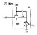
図16A乃至図16Dは、表示デバイスを有する回路を説明する図である。
図17A、図17Bは、画素を説明する図である。
図18は、シミュレーションに用いた回路を説明する図である。
図19は、シミュレーション結果を説明する図である。
図20A乃至図20Cは、表示装置を説明する図である。
図21A、図21Bは、タッチパネルを説明する図である。
図22A、図22Bは、表示装置を説明する図である。
図23は、表示装置を説明する図である。
図24A、図24Bは、表示装置を説明する図である。
図25A、図25Bは、表示装置を説明する図である。
図26A乃至図26Eは、表示装置を説明する図である。
図27A1乃至図27C2は、トランジスタを説明する図である。
図28A1乃至図28C2は、トランジスタを説明する図である。
図29A1乃至図29C2は、トランジスタを説明する図である。
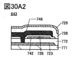
図30A1乃至図30C2は、トランジスタを説明する図である。
図31A乃至図31Fは、電子機器を説明する図である。
本実施の形態では、本発明の一態様である表示装置について、図面を参照して説明する。
図1は、本発明の一態様の表示装置を説明する図である。表示装置は、列方向および行方向に配置された画素10を有する表示領域15と、ソースドライバ12と、ゲートドライバ13と、回路11を有する。ソースドライバ12は、回路11および画素10と電気的に接続される。ゲートドライバ13は、画素10と電気的に接続される。回路11は、画素10と電気的に接続される。なお、ソースドライバ12およびゲートドライバ13は、複数であってもよい。
図3に回路11の構成の一例を示す。回路11は、トランジスタ111と、トランジスタ112と、トランジスタ113と、トランジスタ114と、トランジスタ115と、トランジスタ116と、キャパシタ117と、キャパシタ118を有する構成とすることができる。
画素10は、画像データを生成する回路20と、表示動作を行う回路21を有する構成とすることができる。
回路11では、まず、ノードNAに“+D”(第1のデータ)、ノードNBに“+V1”(例えば、正の電源電位)を書き込む。このとき、キャパシタ117には、“+V1-D1”が保持される。
画素10においては、まず、ノードNMに“+D”(第1のデータ)、ノードNEに“-D”(第2のデータ)を重なるタイミングで書き込む。このとき、キャパシタ117には“+D-(-D)=+2D”が保持される。次に、ノードNMをフローティングとし、ノードNEに“+D”を供給する。
ソースドライバ12および回路11は、図6A、図6B、図6Cに示すように表示領域15の一端側だけでなく、さらに対向する他端側にも設けてもよい。
次に、図7に示すタイミングチャートおよび図8A、図8Bに示す回路動作の説明図を用いて、回路11における反転動作の詳細を説明する。
次に、図9に示すタイミングチャートおよび図10A、図10Bに示す回路動作の説明図を用いて、ソースドライバ12の出力するデータ電位の約3倍のデータ電位を画素10の表示デバイスに供給する方法を説明する。なお、画素10に供給される第2のデータの生成動作の説明は省略する。
図11Aに示す構成は、画素10と2つのソース線との接続関係を入れ替えた構成である。配線127[m_1]には、トランジスタ103のソースまたはドレインの他方が電気的に接続される。配線127[m_2]には、トランジスタ101のソースまたはドレインの他方およびトランジスタ102のソースまたはドレインの他方が電気的に接続される。
図12は、ソースドライバ12および回路11と、画素10との間に選択回路19が設けられた構成である。
ソースドライバ12が第1のデータと、その反転データである第2のデータを出力できる機能を有する場合は、図14に示すように回路11を省いた構成としてもよい。なお、上述した変形例1乃至3は互いに組み合わせることができる。
図15A乃至図15Dは、回路21に適用でき、表示デバイスとして液晶デバイスを含む構成の例である。
また、図17Aに例示するように、本発明の一態様の回路では、バックゲートを設けたトランジスタを用いてもよい。図17Aでは、バックゲートがフロントゲートと電気的に接続された構成を示しており、オン電流を高める効果を有する。または、バックゲートが定電位を供給できる配線と電気的に接続された構成であってもよい。当該構成では、トランジスタのしきい値電圧を制御することができる。なお、回路11および回路21が有するトランジスタにもバックゲートを設けてもよい。
次に、画素の動作に関するシミュレーション結果を説明する。図18にシミュレーションに用いた画素10の構成を示す。図2に示した回路構成を基本とし、回路21としては、液晶デバイス(Clc)およびキャパシタ(Cs)を有する構成を用いた。シミュレーションは、入力電圧を約3倍にする動作におけるノードNMの電圧変化について行った。
本実施の形態では、液晶デバイスを用いた表示装置の構成例と、発光デバイスを用いた表示装置の構成例について説明する。なお、本実施の形態においては、実施の形態1で説明した表示装置の要素、動作および機能の説明は省略する。
本実施の形態では、上記実施の形態に示した各トランジスタに置き換えて用いることのできるトランジスタの一例について、図面を用いて説明する。
図27A1は、ボトムゲート型のトランジスタの一種であるチャネル保護型のトランジスタ810のチャネル長方向の断面図である。図27A1において、トランジスタ810は基板771上に形成されている。また、トランジスタ810は、基板771上に絶縁層772を介して電極746を有する。また、電極746上に絶縁層726を介して半導体層742を有する。電極746はゲート電極として機能できる。絶縁層726はゲート絶縁層として機能できる。
図29A1に例示するトランジスタ842は、トップゲート型のトランジスタの1つである。電極744aおよび電極744bは、絶縁層728および絶縁層729に形成した開口部において半導体層742と電気的に接続する。
本発明の一態様に係る表示装置を用いることができる電子機器として、表示機器、パーソナルコンピュータ、記録媒体を備えた画像記憶装置または画像再生装置、携帯電話、携帯型を含むゲーム機、携帯データ端末、電子書籍端末、ビデオカメラ、デジタルスチルカメラ等のカメラ、ゴーグル型ディスプレイ(ヘッドマウントディスプレイ)、ナビゲーションシステム、音響再生装置(カーオーディオ、デジタルオーディオプレイヤー等)、複写機、ファクシミリ、プリンタ、プリンタ複合機、現金自動預け入れ払い機(ATM)、自動販売機などが挙げられる。これら電子機器の具体例を図31に示す。
Claims (9)
- 第1の回路と、第2の回路と、画素と、を有する表示装置であって、
前記第1の回路は、第1のデータを前記第2の回路に出力する機能を有し、
前記第1の回路は、前記第1のデータを前記画素に出力する機能を有し、
前記第2の回路は、前記第1のデータに基づいて第2のデータを前記画素に出力する機能を有し、
前記第1のデータの電位をD1、前記第2のデータの電位をD2、基準電位をV0としたとき、V0=(D1+D2)/2の関係にあり、
前記画素は、前記第1のデータおよび前記第2のデータに基づいて第3のデータを生成する機能、および前記第3のデータに応じて表示を行う機能を有し、
前記第2の回路は、第1のトランジスタ乃至第6のトランジスタと、第1のキャパシタと、第2のキャパシタと、を有し、
前記第1のトランジスタのソースまたはドレインの一方は、前記第1のキャパシタの一方の電極と電気的に接続され、
前記第1のトランジスタのソースまたはドレインの他方は、前記第1の回路と電気的に接続され、
前記第1のキャパシタの一方の電極は、前記第2のトランジスタのソースまたはドレインの一方と電気的に接続され、
前記第1のトランジスタのゲートは、前記第3のトランジスタのゲートと電気的に接続され、
前記第3のトランジスタのソースまたはドレインの一方は、前記第1のキャパシタの他方の電極と電気的に接続され、
前記第1のキャパシタの他方の電極は、前記第4のトランジスタのソースまたはドレインの一方と電気的に接続され、
前記第4のトランジスタのゲートは、前記第2のトランジスタのゲートと電気的に接続され、
前記第4のトランジスタのソースまたはドレインの他方は、前記第5のトランジスタのゲートと電気的に接続され、
前記第5のトランジスタのゲートは、前記第2のキャパシタの一方の電極と電気的に接続され、
前記第5のトランジスタのソースまたはドレインの一方は、前記第6のトランジスタのソースまたはドレインの一方と電気的に接続され、
前記第6のトランジスタのソースまたはドレインの一方は、前記画素と電気的に接続される表示装置。 - 請求項1において、
さらに第3の回路を有し、
前記第3の回路は、出力経路の選択機能を有し、
前記第3の回路の入力端子は、前記第2の回路と電気的に接続され、
前記第3の回路の出力端子は、前記画素と電気的に接続される表示装置。 - 請求項1または請求項2において、
前記画素は、第7のトランジスタ乃至第9のトランジスタと、第3のキャパシタと、第4の回路と、を有し、
前記第3のキャパシタの一方の電極は、前記第7のトランジスタのソースまたはドレインの一方と電気的に接続され、
前記第7のトランジスタのソースまたはドレインの一方は、前記第4の回路と電気的に接続され、
前記第3のキャパシタの他方の電極は、前記第8のトランジスタのソースまたはドレインの一方と電気的に接続され、
前記第8のトランジスタのソースまたはドレインの一方は、前記第9のトランジスタのソースまたはドレインの一方と電気的に接続され、
前記第7のトランジスタのソースまたはドレインの他方は、前記第8のトランジスタのソースまたはドレインの他方と電気的に接続され、
前記第8のトランジスタのソースまたはドレインの他方は、前記第2の回路と電気的に接続され、
前記第8のトランジスタのソースまたはドレインの他方は、前記第1の回路と電気的に接続され、
前記第9のトランジスタのソースまたはドレインの他方は、前記第2の回路と電気的に接続され、
前記第4の回路は、表示デバイスを有する表示装置。 - 請求項3において、
前記第9のトランジスタのチャネル幅は、前記第7のトランジスタのチャネル幅および前記第8のトランジスタのチャネル幅よりも小さい表示装置。 - 請求項3または請求項4において、
前記第4の回路は、前記表示デバイスとして液晶デバイスを有し、
前記液晶デバイスの一方の電極は、前記第7のトランジスタのソースまたはドレインの一方と電気的に接続されている表示装置。 - 請求項5において、
さらに第4のキャパシタを有し、
前記第4のキャパシタの一方の電極は、前記液晶デバイスの一方の電極と電気的に接続される表示装置。 - 請求項3または請求項4において、
前記第4の回路は、第10のトランジスタと、第5のキャパシタと、前記表示デバイスとして発光デバイスと、を有し、
前記第10のトランジスタのゲートは、前記第7のトランジスタのソースまたはドレインの一方と電気的に接続され、
前記第10のトランジスタのソースまたはドレインの一方は、前記発光デバイスの一方の電極と電気的に接続され、
前記発光デバイスの一方の電極は、前記第5のキャパシタの一方の電極と電気的に接続され、
前記第5のキャパシタの他方の電極は、前記第10のトランジスタのゲートと電気的に接続される表示装置。 - 請求項1乃至請求項7のいずれか一項において、
前記第2の回路および前記画素がそれぞれ有するトランジスタは、チャネル形成領域に金属酸化物を有し、
前記金属酸化物は、Inと、Znと、M(MはAl、Ti、Ga、Sn、Y、Zr、La、Ce、NdまたはHf)と、を有する表示装置。 - 請求項1乃至請求項8のいずれか一項に記載の表示装置と、カメラと、を有する電子機器。
Priority Applications (2)
| Application Number | Priority Date | Filing Date | Title |
|---|---|---|---|
| JP2024067237A JP2024094375A (ja) | 2018-12-26 | 2024-04-18 | 表示装置 |
| JP2025077730A JP2025109775A (ja) | 2018-12-26 | 2025-05-08 | 表示装置 |
Applications Claiming Priority (3)
| Application Number | Priority Date | Filing Date | Title |
|---|---|---|---|
| JP2018242749 | 2018-12-26 | ||
| JP2018242749 | 2018-12-26 | ||
| PCT/IB2019/060823 WO2020136494A1 (ja) | 2018-12-26 | 2019-12-16 | 表示装置および電子機器 |
Related Child Applications (1)
| Application Number | Title | Priority Date | Filing Date |
|---|---|---|---|
| JP2024067237A Division JP2024094375A (ja) | 2018-12-26 | 2024-04-18 | 表示装置 |
Publications (3)
| Publication Number | Publication Date |
|---|---|
| JPWO2020136494A1 JPWO2020136494A1 (ja) | 2020-07-02 |
| JPWO2020136494A5 JPWO2020136494A5 (ja) | 2022-11-14 |
| JP7477461B2 true JP7477461B2 (ja) | 2024-05-01 |
Family
ID=71127560
Family Applications (3)
| Application Number | Title | Priority Date | Filing Date |
|---|---|---|---|
| JP2020561970A Active JP7477461B2 (ja) | 2018-12-26 | 2019-12-16 | 表示装置および電子機器 |
| JP2024067237A Withdrawn JP2024094375A (ja) | 2018-12-26 | 2024-04-18 | 表示装置 |
| JP2025077730A Withdrawn JP2025109775A (ja) | 2018-12-26 | 2025-05-08 | 表示装置 |
Family Applications After (2)
| Application Number | Title | Priority Date | Filing Date |
|---|---|---|---|
| JP2024067237A Withdrawn JP2024094375A (ja) | 2018-12-26 | 2024-04-18 | 表示装置 |
| JP2025077730A Withdrawn JP2025109775A (ja) | 2018-12-26 | 2025-05-08 | 表示装置 |
Country Status (6)
| Country | Link |
|---|---|
| US (3) | US11373610B2 (ja) |
| JP (3) | JP7477461B2 (ja) |
| KR (1) | KR20210107645A (ja) |
| CN (1) | CN113228327A (ja) |
| TW (1) | TWI851638B (ja) |
| WO (1) | WO2020136494A1 (ja) |
Families Citing this family (1)
| Publication number | Priority date | Publication date | Assignee | Title |
|---|---|---|---|---|
| WO2020128721A1 (ja) | 2018-12-19 | 2020-06-25 | 株式会社半導体エネルギー研究所 | 表示装置および電子機器 |
Citations (9)
| Publication number | Priority date | Publication date | Assignee | Title |
|---|---|---|---|---|
| JP2002277898A (ja) | 2001-01-09 | 2002-09-25 | Sharp Corp | 電子装置およびその駆動方法 |
| JP2003323153A (ja) | 2002-04-26 | 2003-11-14 | Semiconductor Energy Lab Co Ltd | 発光装置 |
| JP2010092036A (ja) | 2008-09-12 | 2010-04-22 | Semiconductor Energy Lab Co Ltd | 表示装置 |
| JP2010266494A (ja) | 2009-05-12 | 2010-11-25 | Sony Corp | 表示装置、表示方法 |
| CN102034443A (zh) | 2009-09-30 | 2011-04-27 | 北京京东方光电科技有限公司 | 提高像素电极电压准确性的方法和阵列基板 |
| JP2012185328A (ja) | 2011-03-04 | 2012-09-27 | Sony Corp | 画素回路、表示パネル、表示装置および電子機器 |
| US20120249509A1 (en) | 2011-03-29 | 2012-10-04 | Samsung Electronics Co., Ltd. | Pixel circuit and method of operating the same |
| CN105304039A (zh) | 2015-08-31 | 2016-02-03 | 友达光电股份有限公司 | 像素驱动电路及其驱动方法 |
| JP2017027012A (ja) | 2015-07-24 | 2017-02-02 | 株式会社ジャパンディスプレイ | 表示装置 |
Family Cites Families (37)
| Publication number | Priority date | Publication date | Assignee | Title |
|---|---|---|---|---|
| JP3311224B2 (ja) | 1994-12-28 | 2002-08-05 | キヤノン株式会社 | 表示素子用反転信号生成回路とそれを用いた表示装置 |
| US5883608A (en) | 1994-12-28 | 1999-03-16 | Canon Kabushiki Kaisha | Inverted signal generation circuit for display device, and display apparatus using the same |
| JP3630489B2 (ja) | 1995-02-16 | 2005-03-16 | 株式会社東芝 | 液晶表示装置 |
| JP4160141B2 (ja) | 1998-01-08 | 2008-10-01 | エルジー ディスプレイ カンパニー リミテッド | 液晶表示装置 |
| JP3705123B2 (ja) * | 2000-12-05 | 2005-10-12 | セイコーエプソン株式会社 | 電気光学装置、階調表示方法および電子機器 |
| WO2004034368A1 (ja) * | 2002-10-11 | 2004-04-22 | Mitsubishi Denki Kabushiki Kaisha | 表示装置 |
| GB0318611D0 (en) | 2003-08-08 | 2003-09-10 | Koninkl Philips Electronics Nv | Circuit for signal amplification and use of the same in active matrix devices |
| EP1998373A3 (en) | 2005-09-29 | 2012-10-31 | Semiconductor Energy Laboratory Co, Ltd. | Semiconductor device having oxide semiconductor layer and manufacturing method thereof |
| JP5078246B2 (ja) | 2005-09-29 | 2012-11-21 | 株式会社半導体エネルギー研究所 | 半導体装置、及び半導体装置の作製方法 |
| JP5064747B2 (ja) | 2005-09-29 | 2012-10-31 | 株式会社半導体エネルギー研究所 | 半導体装置、電気泳動表示装置、表示モジュール、電子機器、及び半導体装置の作製方法 |
| US8310423B2 (en) * | 2008-03-05 | 2012-11-13 | Epson Imaging Devices Corporation | Liquid crystal display device and head-up display |
| KR101746198B1 (ko) * | 2009-09-04 | 2017-06-12 | 가부시키가이샤 한도오따이 에네루기 켄큐쇼 | 표시장치 및 전자기기 |
| TWI427606B (zh) * | 2009-10-20 | 2014-02-21 | Au Optronics Corp | 具畫素資料自我保持機能之液晶顯示裝置與其靜止模式運作方法 |
| EP2494597A4 (en) | 2009-10-30 | 2015-03-18 | Semiconductor Energy Lab | SEMICONDUCTOR COMPONENT |
| KR101761636B1 (ko) * | 2010-07-20 | 2017-07-27 | 삼성디스플레이 주식회사 | 유기전계발광 표시장치 |
| US8878589B2 (en) | 2011-06-30 | 2014-11-04 | Semiconductor Energy Laboratory Co., Ltd. | Semiconductor device and driving method thereof |
| KR101924417B1 (ko) * | 2011-11-24 | 2019-02-21 | 삼성디스플레이 주식회사 | 표시 패널의 구동 방법 및 이를 수행하기 위한 표시 장치 |
| US9583057B2 (en) * | 2012-01-12 | 2017-02-28 | Sharp Kabushiki Kaisha | Pixel circuit and display device |
| JP6108856B2 (ja) | 2012-03-09 | 2017-04-05 | キヤノン株式会社 | 表示装置及びそれを用いた電子機器及び表示装置の駆動方法 |
| KR101970537B1 (ko) * | 2012-04-12 | 2019-04-22 | 삼성디스플레이 주식회사 | 표시 장치 |
| JP6158588B2 (ja) * | 2012-05-31 | 2017-07-05 | 株式会社半導体エネルギー研究所 | 発光装置 |
| TWI483238B (zh) * | 2012-12-07 | 2015-05-01 | Au Optronics Corp | 畫素驅動電路與畫素矩陣 |
| KR20150004554A (ko) * | 2013-07-03 | 2015-01-13 | 삼성디스플레이 주식회사 | 화소 및 이를 이용한 유기전계발광 표시장치 |
| KR102131874B1 (ko) * | 2013-11-04 | 2020-07-09 | 삼성디스플레이 주식회사 | 액정 표시 장치 및 그 구동 방법 |
| TWI529694B (zh) | 2014-08-19 | 2016-04-11 | 友達光電股份有限公司 | 面板驅動電路、液晶畫素資料的升壓電路及驅動其的方法 |
| KR102351664B1 (ko) * | 2015-01-14 | 2022-01-14 | 삼성디스플레이 주식회사 | 유기 발광 표시 장치 |
| US10140940B2 (en) | 2015-07-24 | 2018-11-27 | Japan Display Inc. | Display device |
| US10224386B2 (en) * | 2016-09-23 | 2019-03-05 | Apple Inc. | Display with power supply mesh |
| CN106856210B (zh) * | 2017-02-16 | 2019-08-02 | 北京京东方光电科技有限公司 | 薄膜晶体管及其制作方法、显示基板及显示装置 |
| US10276105B2 (en) * | 2017-06-07 | 2019-04-30 | Qualcomm Incorporated | Reversible bias organic light-emitting diode (OLED) drive circuit without initialization voltage |
| WO2019043483A1 (en) | 2017-08-31 | 2019-03-07 | Semiconductor Energy Laboratory Co., Ltd. | DISPLAY DEVICE AND ELECTRONIC DEVICE |
| US11302278B2 (en) | 2017-09-15 | 2022-04-12 | Semiconductor Energy Laboratory Co., Ltd. | Display device including pixel and electronic device |
| KR102650004B1 (ko) * | 2017-12-11 | 2024-03-21 | 엘지디스플레이 주식회사 | 데이터드라이버 및 그를 이용한 유기발광표시장치 |
| US11120764B2 (en) | 2017-12-21 | 2021-09-14 | Semiconductor Energy Laboratory Co., Ltd. | Display device and electronic device |
| JP6669178B2 (ja) * | 2018-01-30 | 2020-03-18 | セイコーエプソン株式会社 | 電気光学装置及び電子機器 |
| KR102612016B1 (ko) * | 2018-12-13 | 2023-12-07 | 엘지디스플레이 주식회사 | 유기발광 표시장치 |
| WO2020128721A1 (ja) | 2018-12-19 | 2020-06-25 | 株式会社半導体エネルギー研究所 | 表示装置および電子機器 |
-
2019
- 2019-12-16 CN CN201980085884.6A patent/CN113228327A/zh active Pending
- 2019-12-16 WO PCT/IB2019/060823 patent/WO2020136494A1/ja not_active Ceased
- 2019-12-16 KR KR1020217017596A patent/KR20210107645A/ko active Pending
- 2019-12-16 JP JP2020561970A patent/JP7477461B2/ja active Active
- 2019-12-16 US US17/298,999 patent/US11373610B2/en active Active
- 2019-12-23 TW TW108147265A patent/TWI851638B/zh active
-
2022
- 2022-06-21 US US17/844,931 patent/US11842705B2/en active Active
-
2023
- 2023-12-05 US US18/529,032 patent/US12488767B2/en active Active
-
2024
- 2024-04-18 JP JP2024067237A patent/JP2024094375A/ja not_active Withdrawn
-
2025
- 2025-05-08 JP JP2025077730A patent/JP2025109775A/ja not_active Withdrawn
Patent Citations (9)
| Publication number | Priority date | Publication date | Assignee | Title |
|---|---|---|---|---|
| JP2002277898A (ja) | 2001-01-09 | 2002-09-25 | Sharp Corp | 電子装置およびその駆動方法 |
| JP2003323153A (ja) | 2002-04-26 | 2003-11-14 | Semiconductor Energy Lab Co Ltd | 発光装置 |
| JP2010092036A (ja) | 2008-09-12 | 2010-04-22 | Semiconductor Energy Lab Co Ltd | 表示装置 |
| JP2010266494A (ja) | 2009-05-12 | 2010-11-25 | Sony Corp | 表示装置、表示方法 |
| CN102034443A (zh) | 2009-09-30 | 2011-04-27 | 北京京东方光电科技有限公司 | 提高像素电极电压准确性的方法和阵列基板 |
| JP2012185328A (ja) | 2011-03-04 | 2012-09-27 | Sony Corp | 画素回路、表示パネル、表示装置および電子機器 |
| US20120249509A1 (en) | 2011-03-29 | 2012-10-04 | Samsung Electronics Co., Ltd. | Pixel circuit and method of operating the same |
| JP2017027012A (ja) | 2015-07-24 | 2017-02-02 | 株式会社ジャパンディスプレイ | 表示装置 |
| CN105304039A (zh) | 2015-08-31 | 2016-02-03 | 友达光电股份有限公司 | 像素驱动电路及其驱动方法 |
Also Published As
| Publication number | Publication date |
|---|---|
| US20220051639A1 (en) | 2022-02-17 |
| US12488767B2 (en) | 2025-12-02 |
| JP2025109775A (ja) | 2025-07-25 |
| US20220319461A1 (en) | 2022-10-06 |
| JPWO2020136494A1 (ja) | 2020-07-02 |
| US11842705B2 (en) | 2023-12-12 |
| US11373610B2 (en) | 2022-06-28 |
| JP2024094375A (ja) | 2024-07-09 |
| KR20210107645A (ko) | 2021-09-01 |
| CN113228327A (zh) | 2021-08-06 |
| US20240105138A1 (en) | 2024-03-28 |
| WO2020136494A1 (ja) | 2020-07-02 |
| TWI851638B (zh) | 2024-08-11 |
| TW202105347A (zh) | 2021-02-01 |
Similar Documents
| Publication | Publication Date | Title |
|---|---|---|
| JP7488927B2 (ja) | 表示装置 | |
| US11715435B2 (en) | Display apparatus and electronic device | |
| JP7689595B2 (ja) | 表示装置 | |
| JP7487111B2 (ja) | 表示装置および電子機器 | |
| JP2024050929A (ja) | 表示装置 | |
| JP2025109775A (ja) | 表示装置 | |
| JP7618876B2 (ja) | 表示装置 | |
| JP7315572B2 (ja) | 表示装置および電子機器 |
Legal Events
| Date | Code | Title | Description |
|---|---|---|---|
| A521 | Request for written amendment filed |
Free format text: JAPANESE INTERMEDIATE CODE: A523 Effective date: 20221103 |
|
| A621 | Written request for application examination |
Free format text: JAPANESE INTERMEDIATE CODE: A621 Effective date: 20221103 |
|
| A131 | Notification of reasons for refusal |
Free format text: JAPANESE INTERMEDIATE CODE: A131 Effective date: 20231219 |
|
| A521 | Request for written amendment filed |
Free format text: JAPANESE INTERMEDIATE CODE: A523 Effective date: 20231227 |
|
| TRDD | Decision of grant or rejection written | ||
| A01 | Written decision to grant a patent or to grant a registration (utility model) |
Free format text: JAPANESE INTERMEDIATE CODE: A01 Effective date: 20240402 |
|
| A61 | First payment of annual fees (during grant procedure) |
Free format text: JAPANESE INTERMEDIATE CODE: A61 Effective date: 20240418 |
|
| R150 | Certificate of patent or registration of utility model |
Ref document number: 7477461 Country of ref document: JP Free format text: JAPANESE INTERMEDIATE CODE: R150 |