JP7496208B2 - 検出装置 - Google Patents
検出装置 Download PDFInfo
- Publication number
- JP7496208B2 JP7496208B2 JP2019232050A JP2019232050A JP7496208B2 JP 7496208 B2 JP7496208 B2 JP 7496208B2 JP 2019232050 A JP2019232050 A JP 2019232050A JP 2019232050 A JP2019232050 A JP 2019232050A JP 7496208 B2 JP7496208 B2 JP 7496208B2
- Authority
- JP
- Japan
- Prior art keywords
- electrode
- photoelectric conversion
- substrate
- semiconductor layer
- conversion element
- Prior art date
- Legal status (The legal status is an assumption and is not a legal conclusion. Google has not performed a legal analysis and makes no representation as to the accuracy of the status listed.)
- Active
Links
Images




Classifications
-
- H—ELECTRICITY
- H10—SEMICONDUCTOR DEVICES; ELECTRIC SOLID-STATE DEVICES NOT OTHERWISE PROVIDED FOR
- H10F—INORGANIC SEMICONDUCTOR DEVICES SENSITIVE TO INFRARED RADIATION, LIGHT, ELECTROMAGNETIC RADIATION OF SHORTER WAVELENGTH OR CORPUSCULAR RADIATION
- H10F39/00—Integrated devices, or assemblies of multiple devices, comprising at least one element covered by group H10F30/00, e.g. radiation detectors comprising photodiode arrays
- H10F39/80—Constructional details of image sensors
- H10F39/802—Geometry or disposition of elements in pixels, e.g. address-lines or gate electrodes
-
- G—PHYSICS
- G06—COMPUTING OR CALCULATING; COUNTING
- G06V—IMAGE OR VIDEO RECOGNITION OR UNDERSTANDING
- G06V40/00—Recognition of biometric, human-related or animal-related patterns in image or video data
- G06V40/10—Human or animal bodies, e.g. vehicle occupants or pedestrians; Body parts, e.g. hands
- G06V40/12—Fingerprints or palmprints
- G06V40/13—Sensors therefor
- G06V40/1318—Sensors therefor using electro-optical elements or layers, e.g. electroluminescent sensing
-
- H—ELECTRICITY
- H04—ELECTRIC COMMUNICATION TECHNIQUE
- H04N—PICTORIAL COMMUNICATION, e.g. TELEVISION
- H04N25/00—Circuitry of solid-state image sensors [SSIS]; Control thereof
- H04N25/70—SSIS architectures; Circuits associated therewith
-
- H—ELECTRICITY
- H04—ELECTRIC COMMUNICATION TECHNIQUE
- H04N—PICTORIAL COMMUNICATION, e.g. TELEVISION
- H04N25/00—Circuitry of solid-state image sensors [SSIS]; Control thereof
- H04N25/70—SSIS architectures; Circuits associated therewith
- H04N25/76—Addressed sensors, e.g. MOS or CMOS sensors
-
- H—ELECTRICITY
- H10—SEMICONDUCTOR DEVICES; ELECTRIC SOLID-STATE DEVICES NOT OTHERWISE PROVIDED FOR
- H10D—INORGANIC ELECTRIC SEMICONDUCTOR DEVICES
- H10D30/00—Field-effect transistors [FET]
- H10D30/01—Manufacture or treatment
- H10D30/021—Manufacture or treatment of FETs having insulated gates [IGFET]
-
- H—ELECTRICITY
- H10—SEMICONDUCTOR DEVICES; ELECTRIC SOLID-STATE DEVICES NOT OTHERWISE PROVIDED FOR
- H10D—INORGANIC ELECTRIC SEMICONDUCTOR DEVICES
- H10D30/00—Field-effect transistors [FET]
- H10D30/60—Insulated-gate field-effect transistors [IGFET]
- H10D30/67—Thin-film transistors [TFT]
-
- H—ELECTRICITY
- H10—SEMICONDUCTOR DEVICES; ELECTRIC SOLID-STATE DEVICES NOT OTHERWISE PROVIDED FOR
- H10F—INORGANIC SEMICONDUCTOR DEVICES SENSITIVE TO INFRARED RADIATION, LIGHT, ELECTROMAGNETIC RADIATION OF SHORTER WAVELENGTH OR CORPUSCULAR RADIATION
- H10F39/00—Integrated devices, or assemblies of multiple devices, comprising at least one element covered by group H10F30/00, e.g. radiation detectors comprising photodiode arrays
- H10F39/10—Integrated devices
- H10F39/12—Image sensors
-
- H—ELECTRICITY
- H10—SEMICONDUCTOR DEVICES; ELECTRIC SOLID-STATE DEVICES NOT OTHERWISE PROVIDED FOR
- H10F—INORGANIC SEMICONDUCTOR DEVICES SENSITIVE TO INFRARED RADIATION, LIGHT, ELECTROMAGNETIC RADIATION OF SHORTER WAVELENGTH OR CORPUSCULAR RADIATION
- H10F77/00—Constructional details of devices covered by this subclass
- H10F77/20—Electrodes
- H10F77/206—Electrodes for devices having potential barriers
-
- H—ELECTRICITY
- H10—SEMICONDUCTOR DEVICES; ELECTRIC SOLID-STATE DEVICES NOT OTHERWISE PROVIDED FOR
- H10F—INORGANIC SEMICONDUCTOR DEVICES SENSITIVE TO INFRARED RADIATION, LIGHT, ELECTROMAGNETIC RADIATION OF SHORTER WAVELENGTH OR CORPUSCULAR RADIATION
- H10F77/00—Constructional details of devices covered by this subclass
- H10F77/30—Coatings
- H10F77/306—Coatings for devices having potential barriers
- H10F77/331—Coatings for devices having potential barriers for filtering or shielding light, e.g. multicolour filters for photodetectors
- H10F77/334—Coatings for devices having potential barriers for filtering or shielding light, e.g. multicolour filters for photodetectors for shielding light, e.g. light blocking layers or cold shields for infrared detectors
-
- H—ELECTRICITY
- H10—SEMICONDUCTOR DEVICES; ELECTRIC SOLID-STATE DEVICES NOT OTHERWISE PROVIDED FOR
- H10D—INORGANIC ELECTRIC SEMICONDUCTOR DEVICES
- H10D89/00—Aspects of integrated devices not covered by groups H10D84/00 - H10D88/00
- H10D89/60—Integrated devices comprising arrangements for electrical or thermal protection, e.g. protection circuits against electrostatic discharge [ESD]
- H10D89/601—Integrated devices comprising arrangements for electrical or thermal protection, e.g. protection circuits against electrostatic discharge [ESD] for devices having insulated gate electrodes, e.g. for IGFETs or IGBTs
- H10D89/911—Integrated devices comprising arrangements for electrical or thermal protection, e.g. protection circuits against electrostatic discharge [ESD] for devices having insulated gate electrodes, e.g. for IGFETs or IGBTs using passive elements as protective elements
-
- H—ELECTRICITY
- H10—SEMICONDUCTOR DEVICES; ELECTRIC SOLID-STATE DEVICES NOT OTHERWISE PROVIDED FOR
- H10F—INORGANIC SEMICONDUCTOR DEVICES SENSITIVE TO INFRARED RADIATION, LIGHT, ELECTROMAGNETIC RADIATION OF SHORTER WAVELENGTH OR CORPUSCULAR RADIATION
- H10F30/00—Individual radiation-sensitive semiconductor devices in which radiation controls the flow of current through the devices, e.g. photodetectors
- H10F30/20—Individual radiation-sensitive semiconductor devices in which radiation controls the flow of current through the devices, e.g. photodetectors the devices having potential barriers, e.g. phototransistors
- H10F30/21—Individual radiation-sensitive semiconductor devices in which radiation controls the flow of current through the devices, e.g. photodetectors the devices having potential barriers, e.g. phototransistors the devices being sensitive to infrared, visible or ultraviolet radiation
- H10F30/22—Individual radiation-sensitive semiconductor devices in which radiation controls the flow of current through the devices, e.g. photodetectors the devices having potential barriers, e.g. phototransistors the devices being sensitive to infrared, visible or ultraviolet radiation the devices having only one potential barrier, e.g. photodiodes
- H10F30/223—Individual radiation-sensitive semiconductor devices in which radiation controls the flow of current through the devices, e.g. photodetectors the devices having potential barriers, e.g. phototransistors the devices being sensitive to infrared, visible or ultraviolet radiation the devices having only one potential barrier, e.g. photodiodes the potential barrier being a PIN barrier
- H10F30/2235—Individual radiation-sensitive semiconductor devices in which radiation controls the flow of current through the devices, e.g. photodetectors the devices having potential barriers, e.g. phototransistors the devices being sensitive to infrared, visible or ultraviolet radiation the devices having only one potential barrier, e.g. photodiodes the potential barrier being a PIN barrier the devices comprising Group IV amorphous materials
-
- H—ELECTRICITY
- H10—SEMICONDUCTOR DEVICES; ELECTRIC SOLID-STATE DEVICES NOT OTHERWISE PROVIDED FOR
- H10F—INORGANIC SEMICONDUCTOR DEVICES SENSITIVE TO INFRARED RADIATION, LIGHT, ELECTROMAGNETIC RADIATION OF SHORTER WAVELENGTH OR CORPUSCULAR RADIATION
- H10F39/00—Integrated devices, or assemblies of multiple devices, comprising at least one element covered by group H10F30/00, e.g. radiation detectors comprising photodiode arrays
- H10F39/10—Integrated devices
- H10F39/12—Image sensors
- H10F39/18—Complementary metal-oxide-semiconductor [CMOS] image sensors; Photodiode array image sensors
- H10F39/182—Colour image sensors
-
- H—ELECTRICITY
- H10—SEMICONDUCTOR DEVICES; ELECTRIC SOLID-STATE DEVICES NOT OTHERWISE PROVIDED FOR
- H10F—INORGANIC SEMICONDUCTOR DEVICES SENSITIVE TO INFRARED RADIATION, LIGHT, ELECTROMAGNETIC RADIATION OF SHORTER WAVELENGTH OR CORPUSCULAR RADIATION
- H10F39/00—Integrated devices, or assemblies of multiple devices, comprising at least one element covered by group H10F30/00, e.g. radiation detectors comprising photodiode arrays
- H10F39/80—Constructional details of image sensors
- H10F39/803—Pixels having integrated switching, control, storage or amplification elements
- H10F39/8037—Pixels having integrated switching, control, storage or amplification elements the integrated elements comprising a transistor
Landscapes
- Engineering & Computer Science (AREA)
- Multimedia (AREA)
- Signal Processing (AREA)
- Human Computer Interaction (AREA)
- Physics & Mathematics (AREA)
- General Physics & Mathematics (AREA)
- Theoretical Computer Science (AREA)
- Solid State Image Pick-Up Elements (AREA)
- Light Receiving Elements (AREA)
- Transforming Light Signals Into Electric Signals (AREA)
- Thin Film Transistor (AREA)
Description
図1は、第1実施形態に係る検出装置を有する照明装置付き検出機器の概略断面構成を示す断面図である。図1に示すように、照明装置付き検出機器120は、検出装置1と、照明装置121と、接着層125と、カバー部材122と、を有する。検出装置1の表面に垂直な方向において、照明装置121、検出装置1、接着層125、カバー部材122の順に積層されている。
図8は、第2実施形態に係る検出素子を構成するアレイ基板の平面図である。なお、以下の説明では、上述した実施形態で説明したものと同じ構成要素には同一の符号を付して重複する説明は省略する。
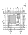
図10は、第3実施形態に係る検出素子を示す平面図である。図10に示すように、第3実施形態の検出素子3Bは、第2電極82Bを有する。なお、図10では、図面を見やすくするために、第2電極82Bを二点鎖線で示している。
2 アレイ基板
3、3A、3B 検出素子
10 センサ部
15 走査線駆動回路
16 信号線選択回路
21 基板
22 アンダーコート膜
23、24、25、26、27、28、29 絶縁膜
30 光電変換素子
81 第1電極
82 第2電極
AA 検出領域
Cs、Cad 容量
Cp 寄生容量
GA 周辺領域
GLrst リセット制御走査線
GLrd 読出制御走査線
SL 出力信号線
SLsf 電源信号線
SLrst リセット信号線
Mrst リセットトランジスタ
Msf ソースフォロワトランジスタ
Mrd 読出トランジスタ
Claims (10)
- 基板と、
前記基板に配列された複数の光電変換素子と、
半導体層と、前記半導体層と対向するゲート電極と、を含み、複数の前記光電変換素子のそれぞれに対応して設けられた複数のトランジスタと、
前記基板に垂直な方向で、前記基板と前記光電変換素子との間に設けられ、絶縁膜を介して対向する第1電極と、第2電極と、を有し、
前記第1電極は前記光電変換素子のそれぞれと重なる複数の主部と、隣り合う前記主部を接続する連結部と、を有し、
前記第2電極は前記複数の光電変換素子の各々に島状に形成され、
前記第1電極は、前記ゲート電極と同層であり、
前記第2電極は、前記半導体層と同層であり、
前記第1電極及び前記第2電極の少なくとも一方は、平面視で、角部が面取りされた面取り部を有する
検出装置。 - 基板と、
前記基板に配列された複数の光電変換素子と、
半導体層と、前記半導体層と対向するゲート電極と、前記半導体層と接続されるソース電極と、を含み、複数の前記光電変換素子のそれぞれに対応して設けられた複数のトランジスタと、
前記基板に垂直な方向で、前記基板と前記光電変換素子との間に設けられ、絶縁膜を介して対向する第1電極と、第2電極と、を有し、
前記第1電極は前記光電変換素子のそれぞれと重なる複数の主部と、隣り合う前記主部を接続する連結部と、を有し、
前記第2電極は前記複数の光電変換素子の各々に島状に形成され、
前記第1電極は、前記ゲート電極と同層であり、
前記第2電極は、前記ソース電極と同層であり、
前記第1電極及び前記第2電極の少なくとも一方は、平面視で、角部が面取りされた面取り部を有する
検出装置。 - 前記第1電極及び前記第2電極は、平面視で、複数の前記トランジスタと重ならない領域に設けられ、
前記第1電極及び前記第2電極は、平面視で、前記光電変換素子に重なる
請求項1又は請求項2に記載の検出装置。 - 複数の前記光電変換素子は、第1方向に並んで配列され、
前記第1電極の前記連結部は、前記第1方向に隣り合う前記主部を電気的に接続する
請求項1から請求項3のいずれか1項に記載の検出装置。 - 基板と、
前記基板に配列された複数の光電変換素子と、
複数の前記光電変換素子のそれぞれに対応して設けられた複数のトランジスタと、
平面視で、前記光電変換素子及び複数の前記トランジスタと重なる領域に設けられ、前記基板に垂直な方向で、絶縁膜を介して対向する第1電極と、第2電極と、を有し、
前記第1電極は、前記光電変換素子の上に設けられ、
前記第2電極は、前記絶縁膜を介して前記第1電極の上に設けられる
検出装置。 - 複数の前記トランジスタを覆う有機絶縁膜と、
前記基板に垂直な方向で、前記有機絶縁膜と前記光電変換素子との間に設けられ、前記光電変換素子と電気的に接続される下部電極と、を有し、
前記第2電極は、前記光電変換素子と重ならない領域に延在し、前記絶縁膜を貫通するコンタクトホールを介して前記下部電極と電気的に接続される
請求項5に記載の検出装置。 - 複数の前記トランジスタに接続される複数の信号線と、複数の走査線とを有し、
前記光電変換素子、前記第1電極及び前記第2電極は、複数の前記信号線と、複数の前記走査線とで囲まれた領域ごとに設けられる
請求項5又は請求項6に記載の検出装置。 - 前記第1電極は、基準電位に接続され、
前記第2電極は、前記トランジスタ及び前記光電変換素子に電気的に接続される
請求項1から請求項7のいずれか1項に記載の検出装置。 - 複数の前記トランジスタは、ソースフォロワトランジスタ、リセットトランジスタ及び読出トランジスタを含み、
前記第2電極は、前記リセットトランジスタのソース又はドレインの一方、及び、前記ソースフォロワトランジスタのゲートに電気的に接続される
請求項1から請求項8のいずれか1項に記載の検出装置。 - 前記光電変換素子は、前記基板の上に積層されたn型半導体層と、i型半導体層と、p型半導体層と、を含む
請求項1から請求項9のいずれか1項に記載の検出装置。
Priority Applications (6)
| Application Number | Priority Date | Filing Date | Title |
|---|---|---|---|
| JP2019232050A JP7496208B2 (ja) | 2019-12-23 | 2019-12-23 | 検出装置 |
| PCT/JP2020/044084 WO2021131483A1 (ja) | 2019-12-23 | 2020-11-26 | 検出装置 |
| CN202080088010.9A CN114830340B (zh) | 2019-12-23 | 2020-11-26 | 检测装置 |
| CN202510635485.XA CN120500129A (zh) | 2019-12-23 | 2020-11-26 | 检测装置 |
| US17/842,236 US12376392B2 (en) | 2019-12-23 | 2022-06-16 | Detection device |
| US18/982,712 US20250120196A1 (en) | 2019-12-23 | 2024-12-16 | Detection device |
Applications Claiming Priority (1)
| Application Number | Priority Date | Filing Date | Title |
|---|---|---|---|
| JP2019232050A JP7496208B2 (ja) | 2019-12-23 | 2019-12-23 | 検出装置 |
Publications (2)
| Publication Number | Publication Date |
|---|---|
| JP2021100081A JP2021100081A (ja) | 2021-07-01 |
| JP7496208B2 true JP7496208B2 (ja) | 2024-06-06 |
Family
ID=76541404
Family Applications (1)
| Application Number | Title | Priority Date | Filing Date |
|---|---|---|---|
| JP2019232050A Active JP7496208B2 (ja) | 2019-12-23 | 2019-12-23 | 検出装置 |
Country Status (4)
| Country | Link |
|---|---|
| US (2) | US12376392B2 (ja) |
| JP (1) | JP7496208B2 (ja) |
| CN (2) | CN120500129A (ja) |
| WO (1) | WO2021131483A1 (ja) |
Families Citing this family (2)
| Publication number | Priority date | Publication date | Assignee | Title |
|---|---|---|---|---|
| JP7626687B2 (ja) * | 2021-08-19 | 2025-02-04 | 株式会社ジャパンディスプレイ | 検出装置 |
| JP7751416B2 (ja) * | 2021-08-23 | 2025-10-08 | 株式会社ジャパンディスプレイ | 検出装置 |
Citations (4)
| Publication number | Priority date | Publication date | Assignee | Title |
|---|---|---|---|---|
| JP2000340777A (ja) | 1999-05-26 | 2000-12-08 | Minolta Co Ltd | 受光素子およびその製造方法 |
| JP2008085029A (ja) | 2006-09-27 | 2008-04-10 | Seiko Epson Corp | 光電変換装置 |
| JP2013012696A (ja) | 2011-05-27 | 2013-01-17 | Sony Corp | 光電変換素子および光電変換装置 |
| JP2013205140A (ja) | 2012-03-28 | 2013-10-07 | Sony Corp | 撮像装置および撮像表示システム |
Family Cites Families (10)
| Publication number | Priority date | Publication date | Assignee | Title |
|---|---|---|---|---|
| JP5109684B2 (ja) * | 2007-06-22 | 2012-12-26 | セイコーエプソン株式会社 | 検出装置及び電子機器 |
| KR101094288B1 (ko) * | 2010-01-27 | 2011-12-19 | 삼성모바일디스플레이주식회사 | 엑스레이 검출 장치 |
| KR20120027708A (ko) * | 2010-09-13 | 2012-03-22 | 삼성모바일디스플레이주식회사 | X-선 검출기 패널 |
| JP5912467B2 (ja) * | 2010-12-10 | 2016-04-27 | 株式会社半導体エネルギー研究所 | 光電変換回路及び表示装置 |
| JP2012227316A (ja) * | 2011-04-19 | 2012-11-15 | Mitsubishi Electric Corp | フォトセンサ |
| JP2014112580A (ja) * | 2012-12-05 | 2014-06-19 | Sony Corp | 固体撮像素子および駆動方法 |
| JP6099035B2 (ja) * | 2012-10-12 | 2017-03-22 | Nltテクノロジー株式会社 | 光電変換装置及びその製造方法並びにx線画像検出装置 |
| WO2015087586A1 (ja) * | 2013-12-10 | 2015-06-18 | シャープ株式会社 | 半導体装置およびその製造方法 |
| JP6555468B2 (ja) * | 2015-04-02 | 2019-08-07 | パナソニックIpマネジメント株式会社 | 撮像装置 |
| JP2019041018A (ja) * | 2017-08-25 | 2019-03-14 | ソニー株式会社 | 撮像素子、積層型撮像素子及び固体撮像装置 |
-
2019
- 2019-12-23 JP JP2019232050A patent/JP7496208B2/ja active Active
-
2020
- 2020-11-26 WO PCT/JP2020/044084 patent/WO2021131483A1/ja not_active Ceased
- 2020-11-26 CN CN202510635485.XA patent/CN120500129A/zh active Pending
- 2020-11-26 CN CN202080088010.9A patent/CN114830340B/zh active Active
-
2022
- 2022-06-16 US US17/842,236 patent/US12376392B2/en active Active
-
2024
- 2024-12-16 US US18/982,712 patent/US20250120196A1/en active Pending
Patent Citations (4)
| Publication number | Priority date | Publication date | Assignee | Title |
|---|---|---|---|---|
| JP2000340777A (ja) | 1999-05-26 | 2000-12-08 | Minolta Co Ltd | 受光素子およびその製造方法 |
| JP2008085029A (ja) | 2006-09-27 | 2008-04-10 | Seiko Epson Corp | 光電変換装置 |
| JP2013012696A (ja) | 2011-05-27 | 2013-01-17 | Sony Corp | 光電変換素子および光電変換装置 |
| JP2013205140A (ja) | 2012-03-28 | 2013-10-07 | Sony Corp | 撮像装置および撮像表示システム |
Also Published As
| Publication number | Publication date |
|---|---|
| CN114830340B (zh) | 2025-05-16 |
| CN114830340A (zh) | 2022-07-29 |
| CN120500129A (zh) | 2025-08-15 |
| US20220328539A1 (en) | 2022-10-13 |
| WO2021131483A1 (ja) | 2021-07-01 |
| US20250120196A1 (en) | 2025-04-10 |
| JP2021100081A (ja) | 2021-07-01 |
| US12376392B2 (en) | 2025-07-29 |
Similar Documents
| Publication | Publication Date | Title |
|---|---|---|
| JP7664447B2 (ja) | 検出装置 | |
| JP7642116B2 (ja) | 検出装置 | |
| JP7529455B2 (ja) | 検出装置 | |
| CN216435906U (zh) | 检测装置 | |
| US20220366720A1 (en) | Biometric authentication device | |
| US20250120196A1 (en) | Detection device | |
| CN114342079B (zh) | 检测装置 | |
| JP7443077B2 (ja) | 検出装置 | |
| JP7550952B2 (ja) | 検出装置 | |
| JP2022029179A (ja) | 検出装置 | |
| JP7633006B2 (ja) | 検出装置 | |
| JP7598710B2 (ja) | 検出装置 | |
| US12457815B2 (en) | Detection device |
Legal Events
| Date | Code | Title | Description |
|---|---|---|---|
| A621 | Written request for application examination |
Free format text: JAPANESE INTERMEDIATE CODE: A621 Effective date: 20221020 |
|
| A131 | Notification of reasons for refusal |
Free format text: JAPANESE INTERMEDIATE CODE: A131 Effective date: 20231219 |
|
| A521 | Request for written amendment filed |
Free format text: JAPANESE INTERMEDIATE CODE: A523 Effective date: 20240119 |
|
| TRDD | Decision of grant or rejection written | ||
| A01 | Written decision to grant a patent or to grant a registration (utility model) |
Free format text: JAPANESE INTERMEDIATE CODE: A01 Effective date: 20240507 |
|
| A61 | First payment of annual fees (during grant procedure) |
Free format text: JAPANESE INTERMEDIATE CODE: A61 Effective date: 20240527 |
|
| R150 | Certificate of patent or registration of utility model |
Ref document number: 7496208 Country of ref document: JP Free format text: JAPANESE INTERMEDIATE CODE: R150 |
|
| S111 | Request for change of ownership or part of ownership |
Free format text: JAPANESE INTERMEDIATE CODE: R313113 |
|
| R350 | Written notification of registration of transfer |
Free format text: JAPANESE INTERMEDIATE CODE: R350 |