JP7500911B2 - キャリア基板へ有用層を移転するためのプロセス - Google Patents
キャリア基板へ有用層を移転するためのプロセス Download PDFInfo
- Publication number
- JP7500911B2 JP7500911B2 JP2021555273A JP2021555273A JP7500911B2 JP 7500911 B2 JP7500911 B2 JP 7500911B2 JP 2021555273 A JP2021555273 A JP 2021555273A JP 2021555273 A JP2021555273 A JP 2021555273A JP 7500911 B2 JP7500911 B2 JP 7500911B2
- Authority
- JP
- Japan
- Prior art keywords
- laminated structure
- carrier substrate
- transferring
- useful layer
- donor substrate
- Prior art date
- Legal status (The legal status is an assumption and is not a legal conclusion. Google has not performed a legal analysis and makes no representation as to the accuracy of the status listed.)
- Active
Links
Images




Classifications
-
- H—ELECTRICITY
- H10—SEMICONDUCTOR DEVICES; ELECTRIC SOLID-STATE DEVICES NOT OTHERWISE PROVIDED FOR
- H10P—GENERIC PROCESSES OR APPARATUS FOR THE MANUFACTURE OR TREATMENT OF DEVICES COVERED BY CLASS H10
- H10P90/00—Preparation of wafers not covered by a single main group of this subclass, e.g. wafer reinforcement
- H10P90/19—Preparing inhomogeneous wafers
- H10P90/1904—Preparing vertically inhomogeneous wafers
- H10P90/1906—Preparing SOI wafers
- H10P90/1914—Preparing SOI wafers using bonding
- H10P90/1916—Preparing SOI wafers using bonding with separation or delamination along an ion implanted layer, e.g. Smart-cut
-
- H—ELECTRICITY
- H10—SEMICONDUCTOR DEVICES; ELECTRIC SOLID-STATE DEVICES NOT OTHERWISE PROVIDED FOR
- H10P—GENERIC PROCESSES OR APPARATUS FOR THE MANUFACTURE OR TREATMENT OF DEVICES COVERED BY CLASS H10
- H10P52/00—Grinding, lapping or polishing of wafers, substrates or parts of devices
-
- H—ELECTRICITY
- H10—SEMICONDUCTOR DEVICES; ELECTRIC SOLID-STATE DEVICES NOT OTHERWISE PROVIDED FOR
- H10P—GENERIC PROCESSES OR APPARATUS FOR THE MANUFACTURE OR TREATMENT OF DEVICES COVERED BY CLASS H10
- H10P54/00—Cutting or separating of wafers, substrates or parts of devices
- H10P54/50—Cutting or separating of wafers, substrates or parts of devices by scoring, breaking or cleaving
- H10P54/52—Cutting or separating of wafers, substrates or parts of devices by scoring, breaking or cleaving by cleaving
-
- H—ELECTRICITY
- H10—SEMICONDUCTOR DEVICES; ELECTRIC SOLID-STATE DEVICES NOT OTHERWISE PROVIDED FOR
- H10P—GENERIC PROCESSES OR APPARATUS FOR THE MANUFACTURE OR TREATMENT OF DEVICES COVERED BY CLASS H10
- H10P95/00—Generic processes or apparatus for manufacture or treatments not covered by the other groups of this subclass
- H10P95/11—Separation of active layers from substrates
-
- H—ELECTRICITY
- H10—SEMICONDUCTOR DEVICES; ELECTRIC SOLID-STATE DEVICES NOT OTHERWISE PROVIDED FOR
- H10W—GENERIC PACKAGES, INTERCONNECTIONS, CONNECTORS OR OTHER CONSTRUCTIONAL DETAILS OF DEVICES COVERED BY CLASS H10
- H10W10/00—Isolation regions in semiconductor bodies between components of integrated devices
- H10W10/10—Isolation regions comprising dielectric materials
- H10W10/181—Semiconductor-on-insulator [SOI] isolation regions, e.g. buried oxide regions of SOI wafers
Landscapes
- Recrystallisation Techniques (AREA)
- Pressure Welding/Diffusion-Bonding (AREA)
- Manufacturing Of Printed Wiring (AREA)
- Macromolecular Compounds Obtained By Forming Nitrogen-Containing Linkages In General (AREA)
- Laminated Bodies (AREA)
Description
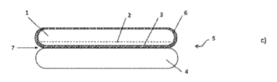
埋め込み弱化平面とドナー基板の表面との間に有用層3を形成するようにドナー基板1へと軽元素種を注入することにより埋め込み弱化平面2を形成するステップと、
次に、キャリア基板4にドナー基板1を接合して、貼り合わせ構造体5を形成するステップと、
次いで、埋め込み弱化平面を弱くするために貼り合わせ構造体5に熱処理を適用するステップと、
そして最後に、埋め込み弱化平面2に沿ってドナー基板1内の分割波の自己維持型の伝播をともなう分割波を惹起するステップと
を含む。
a)埋め込み弱化平面を含んでいるドナー基板を用意するステップであって、前記有用層が前記ドナー基板の前面と前記埋め込み弱化平面とにより範囲を定められている、ドナー基板を用意するステップと、
b)キャリア基板を用意するステップと、
c)貼り合わせ構造体を形成するためにボンディング界面に沿って前記キャリア基板に、前記ドナー基板の前面で、前記ドナー基板を接合するステップと、
d)前記貼り合わせ構造体に弱化サーマルバジェットを加えるため及び定められた弱化のレベルまで前記埋め込み弱化平面を持っていくために前記貼り合わせ構造体をアニールするステップであって、前記アニールが最高保持温度に達する、前記貼り合わせ構造体をアニールするステップと、
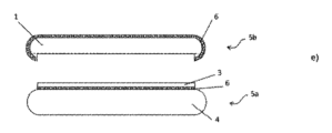
e)前記貼り合わせ構造体に圧力を加えることにより前記埋め込み弱化平面内に分割波を惹起するステップであって、前記有用層が前記キャリア基板へ移転されるという結果をもたらすために、前記分割波が前記埋め込み弱化平面に沿って自己維持型の方式で伝播する、分割波を惹起するステップと
を含む。
前記熱勾配が、20℃と100℃との間、好ましくは60℃と90℃との間、より好ましくは約80℃であるように選択され、
前記最高保持温度が、300℃と600℃との間であり、
アニールするステップd)が、熱処理装置で行われ、ステップe)の前記惹起は、前記貼り合わせ構造体が前記熱処理装置を出るときに生じ、
前記熱処理装置が、複数の貼り合わせ構造体をバッチ処理するために適した横型又は縦型に構成された炉であり、
ステップe)の前記惹起は、前記貼り合わせ構造体の前記ホット領域が150℃と250℃との間の温度に達するときに生じ、
前記弱化サーマルバジェットが、分割サーマルバジェットの40%と95%との間であり、前記分割サーマルバジェットが、前記アニール中に前記埋め込み弱化平面内に前記分割波の自発的な惹起をもたらし、
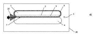
前記圧力が、前記貼り合わせ構造体の、それぞれ前記ドナー基板及び前記キャリア基板の面取りした端部同士の間の前記貼り合わせ構造体の前記ボンディング界面のところにくさびを挿入することによって前記貼り合わせ構造体の周辺部のところに加えられ、
前記ドナー基板及び前記キャリア基板が単結晶シリコン製であり、前記埋め込み弱化平面が前記ドナー基板への軽元素種のイオン注入によって形成され、前記軽元素種が、水素及びヘリウム、又は水素とヘリウムとの組合せから選択される。
発明による移転プロセスは、SOI基板の製造に使用されることがあり、その有用層3は非常に薄く、特に数nmと50nmとの間である。使用した例は、そのドナー基板1及びキャリア基板4が単結晶シリコン製のものであり、各々が直径300mmウェハの形態を取っている。ドナー基板は、50nmの厚さを有する酸化シリコン6の層で覆われている。埋め込み弱化平面2が、下記の条件下で水素イオン及びヘリウムイオンの共注入によりドナー基板1内に形成されている:
H:注入エネルギー38keV、ドーズ1E16 H/cm2、
He:注入エネルギー25keV、ドーズ1E16 He/cm2。
Claims (9)
- キャリア基板(4)へ有用層(3)を移転するためのプロセスであって、
a)埋め込み弱化平面(2)を含んでいるドナー基板(1)を用意するステップであり、前記有用層(3)が前記ドナー基板(1)の前面(1a)と前記埋め込み弱化平面(2)とにより範囲を定められている、ドナー基板(1)を用意するステップと、
b)キャリア基板(4)を用意するステップと、
c)貼り合わせ構造体(5)を形成するためにボンディング界面(7)に沿って前記キャリア基板(4)に、前記ドナー基板(1)の前面(1a)で、前記ドナー基板(1)を接合するステップと、
d)前記貼り合わせ構造体(5)に弱化サーマルバジェットを加えるため及び定められた弱化のレベルまで前記埋め込み弱化平面(2)を持っていくために前記貼り合わせ構造体(5)をアニールするステップであり、前記アニールが最高保持温度に達する、前記貼り合わせ構造体(5)をアニールするステップと、
e)前記貼り合わせ構造体(5)に圧力を加えることにより前記埋め込み弱化平面(2)内に分割波を惹起するステップであり、前記有用層(3)が前記キャリア基板(4)へ移転されるという結果をもたらすために、前記分割波が前記埋め込み弱化平面(2)に沿って自己維持型の方式で伝播する、分割波を惹起するステップと、
を含む、移転するためのプロセスにおいて、
前記移転プロセスは、前記貼り合わせ構造体(5)が、前記貼り合わせ構造体(5)のホット領域及びクール領域を定めている熱勾配を経験しているときに、ステップe)の惹起が生じ、前記圧力が前記クール領域に局所的に加えられ、前記ホット領域が最高保持温度よりも低い温度を経験していることを特徴とする、移転するためのプロセス。 - 前記熱勾配が、20℃と100℃との間であるように選択される、請求項1に記載の移転するためのプロセス。
- 前記最高保持温度が、300℃と600℃との間である、請求項1又は2に記載の移転するためのプロセス。
- アニールするステップd)が、熱処理装置(20)で行われ、ステップe)の前記惹起は、前記貼り合わせ構造体(5)が前記熱処理装置(20)を出るときに生じる、請求項1~3のいずれか一項に記載の移転するためのプロセス。
- 前記熱処理装置(20)が、複数の貼り合わせ構造体(5)をバッチ処理するために適した横型又は縦型に構成された炉である、請求項4に記載の移転するためのプロセス。
- ステップe)の前記惹起は、前記貼り合わせ構造体(5)の前記ホット領域が150℃と250℃との間の温度に達するときに生じる、請求項1~5のいずれか一項に記載の移転するためのプロセス。
- 前記弱化サーマルバジェットが、分割サーマルバジェットの40%と95%との間であり、前記分割サーマルバジェットが、前記アニール中に前記埋め込み弱化平面(2)内に前記分割波の自発的な惹起をもたらす、請求項1~6のいずれか一項に記載の移転するためのプロセス。
- 前記圧力が、前記貼り合わせ構造体(5)の、それぞれ前記ドナー基板(1)及び前記キャリア基板(4)の面取りした端部同士の間の前記貼り合わせ構造体(5)の前記ボンディング界面(7)のところにくさび(10)を挿入することによって前記貼り合わせ構造体(5)の周辺部のところに加えられる、請求項1~7のいずれか一項に記載の移転するためのプロセス。
- 前記ドナー基板(1)及び前記キャリア基板(4)が単結晶シリコン製であり、前記埋め込み弱化平面(2)が前記ドナー基板(1)への軽元素種のイオン注入によって形成され、前記軽元素種が、水素及びヘリウム、又は水素とヘリウムとの組合せから選択される、請求項1~8のいずれか一項に記載の移転するためのプロセス。
Applications Claiming Priority (3)
| Application Number | Priority Date | Filing Date | Title |
|---|---|---|---|
| FR1902674 | 2019-03-15 | ||
| FR1902674A FR3093859B1 (fr) | 2019-03-15 | 2019-03-15 | Procédé de transfert d’une couche utile sur une substrat support |
| PCT/FR2020/050369 WO2020188169A1 (fr) | 2019-03-15 | 2020-02-26 | Procede de transfert d'une couche utile sur une substrat support |
Publications (2)
| Publication Number | Publication Date |
|---|---|
| JP2022527048A JP2022527048A (ja) | 2022-05-30 |
| JP7500911B2 true JP7500911B2 (ja) | 2024-06-18 |
Family
ID=67384010
Family Applications (1)
| Application Number | Title | Priority Date | Filing Date |
|---|---|---|---|
| JP2021555273A Active JP7500911B2 (ja) | 2019-03-15 | 2020-02-26 | キャリア基板へ有用層を移転するためのプロセス |
Country Status (9)
| Country | Link |
|---|---|
| US (1) | US11876015B2 (ja) |
| EP (1) | EP3939078A1 (ja) |
| JP (1) | JP7500911B2 (ja) |
| KR (1) | KR102855947B1 (ja) |
| CN (1) | CN113491004B (ja) |
| FR (1) | FR3093859B1 (ja) |
| SG (1) | SG11202109921QA (ja) |
| TW (1) | TWI824112B (ja) |
| WO (1) | WO2020188169A1 (ja) |
Families Citing this family (3)
| Publication number | Priority date | Publication date | Assignee | Title |
|---|---|---|---|---|
| FR3134229B1 (fr) * | 2022-04-01 | 2024-03-08 | Commissariat Energie Atomique | Procede de transfert d’une couche mince sur un substrat support |
| TWI904594B (zh) * | 2024-03-07 | 2025-11-11 | 鴻揚半導體股份有限公司 | 碳化矽晶圓的製造方法 |
| CN120358922B (zh) * | 2025-04-16 | 2025-11-21 | 达波科技(上海)有限公司 | 一种晶圆复合薄膜及其制备方法 |
Citations (5)
| Publication number | Priority date | Publication date | Assignee | Title |
|---|---|---|---|---|
| JP2004214399A (ja) | 2002-12-27 | 2004-07-29 | Sumitomo Mitsubishi Silicon Corp | 半導体基板の製造方法およびウェーハ剥離熱処理装置 |
| JP2005354078A (ja) | 2004-06-10 | 2005-12-22 | Soi Tec Silicon On Insulator Technologies | 材料複合体ウェーハの製造方法 |
| JP2007510298A (ja) | 2003-10-28 | 2007-04-19 | エス オー イ テク シリコン オン インシュレータ テクノロジース | 注入又は共注入後のパルスによる薄膜層の自立転写方法 |
| JP2012186292A (ja) | 2011-03-04 | 2012-09-27 | Shin Etsu Handotai Co Ltd | 貼り合わせウェーハの製造方法 |
| JP2015213161A (ja) | 2014-04-16 | 2015-11-26 | ソイテックSoitec | 有用層を移転するための方法 |
Family Cites Families (11)
| Publication number | Priority date | Publication date | Assignee | Title |
|---|---|---|---|---|
| FR2839385B1 (fr) * | 2002-05-02 | 2004-07-23 | Soitec Silicon On Insulator | Procede de decollement de couches de materiau |
| US7456080B2 (en) * | 2005-12-19 | 2008-11-25 | Corning Incorporated | Semiconductor on glass insulator made using improved ion implantation process |
| US8993410B2 (en) | 2006-09-08 | 2015-03-31 | Silicon Genesis Corporation | Substrate cleaving under controlled stress conditions |
| US8293619B2 (en) * | 2008-08-28 | 2012-10-23 | Silicon Genesis Corporation | Layer transfer of films utilizing controlled propagation |
| FR2912259B1 (fr) * | 2007-02-01 | 2009-06-05 | Soitec Silicon On Insulator | Procede de fabrication d'un substrat du type "silicium sur isolant". |
| FR2938120B1 (fr) * | 2008-10-31 | 2011-04-08 | Commissariat Energie Atomique | Procede de formation d'une couche monocristalline dans le domaine micro-electronique |
| US8357974B2 (en) * | 2010-06-30 | 2013-01-22 | Corning Incorporated | Semiconductor on glass substrate with stiffening layer and process of making the same |
| US9214353B2 (en) * | 2012-02-26 | 2015-12-15 | Solexel, Inc. | Systems and methods for laser splitting and device layer transfer |
| US9257339B2 (en) * | 2012-05-04 | 2016-02-09 | Silicon Genesis Corporation | Techniques for forming optoelectronic devices |
| JP6396853B2 (ja) * | 2015-06-02 | 2018-09-26 | 信越化学工業株式会社 | 酸化物単結晶薄膜を備えた複合ウェーハの製造方法 |
| JP6563360B2 (ja) * | 2016-04-05 | 2019-08-21 | 信越化学工業株式会社 | 酸化物単結晶薄膜を備えた複合ウェーハの製造方法 |
-
2019
- 2019-03-15 FR FR1902674A patent/FR3093859B1/fr active Active
-
2020
- 2020-02-24 TW TW109105911A patent/TWI824112B/zh active
- 2020-02-26 EP EP20713948.6A patent/EP3939078A1/fr active Pending
- 2020-02-26 WO PCT/FR2020/050369 patent/WO2020188169A1/fr not_active Ceased
- 2020-02-26 KR KR1020217032935A patent/KR102855947B1/ko active Active
- 2020-02-26 SG SG11202109921Q patent/SG11202109921QA/en unknown
- 2020-02-26 JP JP2021555273A patent/JP7500911B2/ja active Active
- 2020-02-26 CN CN202080016748.4A patent/CN113491004B/zh active Active
- 2020-02-26 US US17/435,631 patent/US11876015B2/en active Active
Patent Citations (5)
| Publication number | Priority date | Publication date | Assignee | Title |
|---|---|---|---|---|
| JP2004214399A (ja) | 2002-12-27 | 2004-07-29 | Sumitomo Mitsubishi Silicon Corp | 半導体基板の製造方法およびウェーハ剥離熱処理装置 |
| JP2007510298A (ja) | 2003-10-28 | 2007-04-19 | エス オー イ テク シリコン オン インシュレータ テクノロジース | 注入又は共注入後のパルスによる薄膜層の自立転写方法 |
| JP2005354078A (ja) | 2004-06-10 | 2005-12-22 | Soi Tec Silicon On Insulator Technologies | 材料複合体ウェーハの製造方法 |
| JP2012186292A (ja) | 2011-03-04 | 2012-09-27 | Shin Etsu Handotai Co Ltd | 貼り合わせウェーハの製造方法 |
| JP2015213161A (ja) | 2014-04-16 | 2015-11-26 | ソイテックSoitec | 有用層を移転するための方法 |
Also Published As
| Publication number | Publication date |
|---|---|
| SG11202109921QA (en) | 2021-10-28 |
| TW202036784A (zh) | 2020-10-01 |
| US20220157650A1 (en) | 2022-05-19 |
| FR3093859A1 (fr) | 2020-09-18 |
| TWI824112B (zh) | 2023-12-01 |
| CN113491004B (zh) | 2024-09-13 |
| KR102855947B1 (ko) | 2025-09-05 |
| JP2022527048A (ja) | 2022-05-30 |
| KR20210134784A (ko) | 2021-11-10 |
| CN113491004A (zh) | 2021-10-08 |
| FR3093859B1 (fr) | 2021-02-12 |
| WO2020188169A1 (fr) | 2020-09-24 |
| US11876015B2 (en) | 2024-01-16 |
| EP3939078A1 (fr) | 2022-01-19 |
Similar Documents
| Publication | Publication Date | Title |
|---|---|---|
| US6969668B1 (en) | Treatment method of film quality for the manufacture of substrates | |
| US7449394B2 (en) | Atomic implantation and thermal treatment of a semiconductor layer | |
| JP4425631B2 (ja) | 超小型構成部品を含む薄膜層を製造するための方法 | |
| JP7500911B2 (ja) | キャリア基板へ有用層を移転するためのプロセス | |
| JP2010219566A (ja) | 所望の基板への単結晶材料からなる薄層の移動方法 | |
| EP1429381A2 (en) | A method for manufacturing a material compound | |
| JP5025957B2 (ja) | 欠陥クラスタを有する基板内に形成された薄い層を転写する方法 | |
| JP2006527480A (ja) | 自立を誘発することによって薄肉化された極薄層の製造方法 | |
| JP7510434B2 (ja) | キャリア基板へ有用層を移転するためのプロセス | |
| EP1831922B9 (en) | Method for obtaining a thin layer having a low density of holes | |
| JP7605748B2 (ja) | キャリア基板へ有用層を移転するためのプロセス | |
| US20110256730A1 (en) | Finishing method for manufacturing substrates in the field of electronics | |
| EP2130217B1 (en) | Improving the quality of a thin layer through high-temperature thermal annealing | |
| US7098148B2 (en) | Method for heat treating a semiconductor wafer | |
| TW202335092A (zh) | 用於將薄層移轉至載體底材之方法 | |
| CN119156697A (zh) | 用于将薄膜转移到支撑衬底上的方法 | |
| WO2007071787A1 (en) | Process for simplification of a finishing sequence and structure obtained by the process |
Legal Events
| Date | Code | Title | Description |
|---|---|---|---|
| A521 | Request for written amendment filed |
Free format text: JAPANESE INTERMEDIATE CODE: A523 Effective date: 20220426 |
|
| A521 | Request for written amendment filed |
Free format text: JAPANESE INTERMEDIATE CODE: A821 Effective date: 20220426 |
|
| A621 | Written request for application examination |
Free format text: JAPANESE INTERMEDIATE CODE: A621 Effective date: 20221220 |
|
| A131 | Notification of reasons for refusal |
Free format text: JAPANESE INTERMEDIATE CODE: A131 Effective date: 20240130 |
|
| A977 | Report on retrieval |
Free format text: JAPANESE INTERMEDIATE CODE: A971007 Effective date: 20240131 |
|
| A521 | Request for written amendment filed |
Free format text: JAPANESE INTERMEDIATE CODE: A523 Effective date: 20240304 |
|
| TRDD | Decision of grant or rejection written | ||
| A01 | Written decision to grant a patent or to grant a registration (utility model) |
Free format text: JAPANESE INTERMEDIATE CODE: A01 Effective date: 20240507 |
|
| A61 | First payment of annual fees (during grant procedure) |
Free format text: JAPANESE INTERMEDIATE CODE: A61 Effective date: 20240515 |
|
| R150 | Certificate of patent or registration of utility model |
Ref document number: 7500911 Country of ref document: JP Free format text: JAPANESE INTERMEDIATE CODE: R150 |