JP7524736B2 - SUBSTRATE PROCESSING APPARATUS, SUBSTRATE PROCESSING METHOD, AND STORAGE MEDIUM - Google Patents
SUBSTRATE PROCESSING APPARATUS, SUBSTRATE PROCESSING METHOD, AND STORAGE MEDIUM Download PDFInfo
- Publication number
- JP7524736B2 JP7524736B2 JP2020195422A JP2020195422A JP7524736B2 JP 7524736 B2 JP7524736 B2 JP 7524736B2 JP 2020195422 A JP2020195422 A JP 2020195422A JP 2020195422 A JP2020195422 A JP 2020195422A JP 7524736 B2 JP7524736 B2 JP 7524736B2
- Authority
- JP
- Japan
- Prior art keywords
- processing
- substrate
- block
- processing block
- carrier
- Prior art date
- Legal status (The legal status is an assumption and is not a legal conclusion. Google has not performed a legal analysis and makes no representation as to the accuracy of the status listed.)
- Active
Links
Images




Classifications
-
- H—ELECTRICITY
- H10—SEMICONDUCTOR DEVICES; ELECTRIC SOLID-STATE DEVICES NOT OTHERWISE PROVIDED FOR
- H10P—GENERIC PROCESSES OR APPARATUS FOR THE MANUFACTURE OR TREATMENT OF DEVICES COVERED BY CLASS H10
- H10P72/00—Handling or holding of wafers, substrates or devices during manufacture or treatment thereof
- H10P72/04—Apparatus for manufacture or treatment
- H10P72/0451—Apparatus for manufacturing or treating in a plurality of work-stations
- H10P72/0452—Apparatus for manufacturing or treating in a plurality of work-stations characterised by the layout of the process chambers
- H10P72/0458—Apparatus for manufacturing or treating in a plurality of work-stations characterised by the layout of the process chambers vertical arrangement
-
- H—ELECTRICITY
- H10—SEMICONDUCTOR DEVICES; ELECTRIC SOLID-STATE DEVICES NOT OTHERWISE PROVIDED FOR
- H10P—GENERIC PROCESSES OR APPARATUS FOR THE MANUFACTURE OR TREATMENT OF DEVICES COVERED BY CLASS H10
- H10P72/00—Handling or holding of wafers, substrates or devices during manufacture or treatment thereof
- H10P72/04—Apparatus for manufacture or treatment
- H10P72/0451—Apparatus for manufacturing or treating in a plurality of work-stations
-
- H—ELECTRICITY
- H10—SEMICONDUCTOR DEVICES; ELECTRIC SOLID-STATE DEVICES NOT OTHERWISE PROVIDED FOR
- H10P—GENERIC PROCESSES OR APPARATUS FOR THE MANUFACTURE OR TREATMENT OF DEVICES COVERED BY CLASS H10
- H10P72/00—Handling or holding of wafers, substrates or devices during manufacture or treatment thereof
- H10P72/04—Apparatus for manufacture or treatment
- H10P72/0402—Apparatus for fluid treatment
-
- H—ELECTRICITY
- H10—SEMICONDUCTOR DEVICES; ELECTRIC SOLID-STATE DEVICES NOT OTHERWISE PROVIDED FOR
- H10P—GENERIC PROCESSES OR APPARATUS FOR THE MANUFACTURE OR TREATMENT OF DEVICES COVERED BY CLASS H10
- H10P72/00—Handling or holding of wafers, substrates or devices during manufacture or treatment thereof
- H10P72/04—Apparatus for manufacture or treatment
- H10P72/0448—Apparatus for applying a liquid, a resin, an ink or the like
-
- H—ELECTRICITY
- H10—SEMICONDUCTOR DEVICES; ELECTRIC SOLID-STATE DEVICES NOT OTHERWISE PROVIDED FOR
- H10P—GENERIC PROCESSES OR APPARATUS FOR THE MANUFACTURE OR TREATMENT OF DEVICES COVERED BY CLASS H10
- H10P72/00—Handling or holding of wafers, substrates or devices during manufacture or treatment thereof
- H10P72/04—Apparatus for manufacture or treatment
- H10P72/0451—Apparatus for manufacturing or treating in a plurality of work-stations
- H10P72/0452—Apparatus for manufacturing or treating in a plurality of work-stations characterised by the layout of the process chambers
-
- H—ELECTRICITY
- H10—SEMICONDUCTOR DEVICES; ELECTRIC SOLID-STATE DEVICES NOT OTHERWISE PROVIDED FOR
- H10P—GENERIC PROCESSES OR APPARATUS FOR THE MANUFACTURE OR TREATMENT OF DEVICES COVERED BY CLASS H10
- H10P72/00—Handling or holding of wafers, substrates or devices during manufacture or treatment thereof
- H10P72/04—Apparatus for manufacture or treatment
- H10P72/0451—Apparatus for manufacturing or treating in a plurality of work-stations
- H10P72/0452—Apparatus for manufacturing or treating in a plurality of work-stations characterised by the layout of the process chambers
- H10P72/0456—Apparatus for manufacturing or treating in a plurality of work-stations characterised by the layout of the process chambers in-line arrangement
-
- H—ELECTRICITY
- H10—SEMICONDUCTOR DEVICES; ELECTRIC SOLID-STATE DEVICES NOT OTHERWISE PROVIDED FOR
- H10P—GENERIC PROCESSES OR APPARATUS FOR THE MANUFACTURE OR TREATMENT OF DEVICES COVERED BY CLASS H10
- H10P72/00—Handling or holding of wafers, substrates or devices during manufacture or treatment thereof
- H10P72/30—Handling or holding of wafers, substrates or devices during manufacture or treatment thereof for conveying, e.g. between different workstations
- H10P72/32—Handling or holding of wafers, substrates or devices during manufacture or treatment thereof for conveying, e.g. between different workstations between different workstations
-
- H—ELECTRICITY
- H10—SEMICONDUCTOR DEVICES; ELECTRIC SOLID-STATE DEVICES NOT OTHERWISE PROVIDED FOR
- H10P—GENERIC PROCESSES OR APPARATUS FOR THE MANUFACTURE OR TREATMENT OF DEVICES COVERED BY CLASS H10
- H10P72/00—Handling or holding of wafers, substrates or devices during manufacture or treatment thereof
- H10P72/30—Handling or holding of wafers, substrates or devices during manufacture or treatment thereof for conveying, e.g. between different workstations
- H10P72/32—Handling or holding of wafers, substrates or devices during manufacture or treatment thereof for conveying, e.g. between different workstations between different workstations
- H10P72/3218—Conveying cassettes, containers or carriers
-
- H—ELECTRICITY
- H10—SEMICONDUCTOR DEVICES; ELECTRIC SOLID-STATE DEVICES NOT OTHERWISE PROVIDED FOR
- H10P—GENERIC PROCESSES OR APPARATUS FOR THE MANUFACTURE OR TREATMENT OF DEVICES COVERED BY CLASS H10
- H10P72/00—Handling or holding of wafers, substrates or devices during manufacture or treatment thereof
- H10P72/30—Handling or holding of wafers, substrates or devices during manufacture or treatment thereof for conveying, e.g. between different workstations
- H10P72/33—Handling or holding of wafers, substrates or devices during manufacture or treatment thereof for conveying, e.g. between different workstations into and out of processing chamber
- H10P72/3302—Mechanical parts of transfer devices
-
- H—ELECTRICITY
- H10—SEMICONDUCTOR DEVICES; ELECTRIC SOLID-STATE DEVICES NOT OTHERWISE PROVIDED FOR
- H10P—GENERIC PROCESSES OR APPARATUS FOR THE MANUFACTURE OR TREATMENT OF DEVICES COVERED BY CLASS H10
- H10P72/00—Handling or holding of wafers, substrates or devices during manufacture or treatment thereof
- H10P72/30—Handling or holding of wafers, substrates or devices during manufacture or treatment thereof for conveying, e.g. between different workstations
- H10P72/34—Handling or holding of wafers, substrates or devices during manufacture or treatment thereof for conveying, e.g. between different workstations the wafers being stored in a carrier, involving loading and unloading
- H10P72/3402—Mechanical parts of transfer devices
-
- H—ELECTRICITY
- H10—SEMICONDUCTOR DEVICES; ELECTRIC SOLID-STATE DEVICES NOT OTHERWISE PROVIDED FOR
- H10P—GENERIC PROCESSES OR APPARATUS FOR THE MANUFACTURE OR TREATMENT OF DEVICES COVERED BY CLASS H10
- H10P72/00—Handling or holding of wafers, substrates or devices during manufacture or treatment thereof
- H10P72/30—Handling or holding of wafers, substrates or devices during manufacture or treatment thereof for conveying, e.g. between different workstations
- H10P72/34—Handling or holding of wafers, substrates or devices during manufacture or treatment thereof for conveying, e.g. between different workstations the wafers being stored in a carrier, involving loading and unloading
- H10P72/3408—Docking arrangements
-
- H—ELECTRICITY
- H10—SEMICONDUCTOR DEVICES; ELECTRIC SOLID-STATE DEVICES NOT OTHERWISE PROVIDED FOR
- H10P—GENERIC PROCESSES OR APPARATUS FOR THE MANUFACTURE OR TREATMENT OF DEVICES COVERED BY CLASS H10
- H10P74/00—Testing or measuring during manufacture or treatment of wafers, substrates or devices
- H10P74/20—Testing or measuring during manufacture or treatment of wafers, substrates or devices characterised by the properties tested or measured, e.g. structural or electrical properties
Landscapes
- Container, Conveyance, Adherence, Positioning, Of Wafer (AREA)
- Engineering & Computer Science (AREA)
- Robotics (AREA)
- Manufacturing & Machinery (AREA)
- Exposure Of Semiconductors, Excluding Electron Or Ion Beam Exposure (AREA)
Description
本開示は、基板処理装置、基板処理方法及び記憶媒体に関する。 The present disclosure relates to a substrate processing apparatus, a substrate processing method, and a storage medium.
半導体デバイスの製造工程においては、半導体ウエハ(以下、ウエハと記載する)について基板処理装置内の各種の処理モジュール間を搬送することで、液処理や加熱処理などの処理が行われる。ウエハはキャリアにより基板処理装置に搬送される。特許文献1には、当該キャリアに対してウエハを受け渡すキャリアブロックを備えた基板処理装置について示されている。このキャリアブロックでは、多数の基板の載置部からなる積層体を挟むように搬送機構が2つ設けられており、各搬送機構は、載置部間でのウエハの受け渡し用の保持部と、キャリアに対してのウエハの受け渡し用の保持部と、を備える。
In the manufacturing process of semiconductor devices, semiconductor wafers (hereinafter referred to as wafers) are transported between various processing modules in a substrate processing apparatus, where they are subjected to processes such as liquid processing and heat treatment. Wafers are transported to the substrate processing apparatus by a carrier.
本開示は、基板処理装置におけるスループットを高くすると共に、専有床面積を抑えることができる技術を提供する。 This disclosure provides technology that can increase the throughput of substrate processing equipment while reducing the amount of floor space required.
本開示の基板処理装置は、基板を格納するキャリアが載置されるキャリア載置部を備えるキャリアブロックと、
前記基板を各々処理し、互いに積層されて設けられる複数の処理モジュールと、前記複数の処理モジュールに共用されて前記基板を搬送する主搬送機構と、を備え、前記キャリア載置部に対して平面視、左右の一方に設けられる一の処理ブロックと、
前記基板を各々処理し、互いに積層されて設けられる複数の処理モジュールと、前記複数の処理モジュールに共用されて前記基板を搬送する主搬送機構と、を備え、前記一の処理ブロックに対して縦方向に重なる他の処理ブロックと、
平面視、前記キャリア載置部と、前記一の処理ブロック及び前記他の処理ブロックとの間に介在するように、前記キャリアブロックに設けられる前記基板の搬送領域と、
前記キャリアに対して前記基板を受け渡すために前記搬送領域に設けられる第1の搬送機構と、
前記第1の搬送機構、前記一の処理ブロックの主搬送機構、前記他の処理ブロックの主搬送機構によって夫々前記基板が受け渡される第1の載置部、第2の載置部、第3の載置部が互いに縦方向に重なって構成されると共に、平面視、前記第1の搬送機構に対して前後の一方側に設けられる載置部の積層体と、
平面視、前記第1の搬送機構と共に前記積層体を前後から挟むように前記搬送領域に設けられ、前記第1の載置部と前記第2の載置部との間、前記第1の載置部と前記第3の載置部との間で夫々前記基板を搬送するための第2の搬送機構と、
を備える。
The substrate processing apparatus according to the present disclosure includes a carrier block including a carrier placement portion on which a carrier for storing a substrate is placed;
a processing block including a plurality of processing modules each for processing the substrate, the processing block being stacked on top of one another, and a main transport mechanism shared by the plurality of processing modules for transporting the substrate, the processing block being provided on either the left or right side of the carrier placement unit in a plan view;
a plurality of processing modules each for processing the substrate, the processing modules being stacked on top of one another; and a main transport mechanism shared by the plurality of processing modules for transporting the substrate, the main transport mechanism being overlapped in a vertical direction with respect to the first processing block;
a transport region for the substrate provided in the carrier block so as to be interposed between the carrier placement part, the first processing block, and the second processing block in a plan view;
a first transport mechanism provided in the transport region for transferring the substrate to the carrier;
a stack of platform parts, which are configured so that a first platform part, a second platform part, and a third platform part to which the substrate is transferred by the first transport mechanism, the main transport mechanism of the one processing block, and the main transport mechanism of the other processing block, are stacked one on top of the other in the vertical direction, and which are provided on one of the front and rear sides of the first transport mechanism in a plan view;
a second transport mechanism that is provided in the transport region so as to sandwich the stack from the front and rear together with the first transport mechanism in a plan view, and that transports the substrate between the first placement part and the second placement part and between the first placement part and the third placement part, respectively;
Equipped with.
本開示は、基板処理装置におけるスループットを高くすると共に、専有床面積を抑えることができる。 This disclosure can increase the throughput of substrate processing equipment while reducing the amount of floor space required.
本開示の基板処理装置の一実施形態に係る塗布、現像装置1について、図1の横断平面図、図2、図3の縦断正面図を夫々参照して説明する。図2、図3については装置の異なる位置の断面を示している。塗布、現像装置1は、キャリアブロックD1と、第1の処理ブロックD2と、第2の処理ブロックD3と、インターフェイスブロックD4と、がこの順で横方向に直線状に配列され、隣り合うブロック同士が互いに接続されている。これらのブロック(キャリアブロック、第1及び第2の処理ブロック、インターフェイスブロック)D1~D4は各々筐体を備えて互いに区画されており、各筐体の内部に基板であるウエハWの搬送領域が形成されている。
A coating and developing
以降の説明にあたり、これらブロックD1~D4の配列方向を左右方向とし、キャリアブロックD1側を左側、インターフェイスブロックD4を右側とする。また、装置の前後方向について、キャリアブロックD1を左に見たときの手前を前方、奥を後方とする。中継ブロックであるインターフェイスブロックD4には、右側から露光機20が接続されている。
In the following explanation, the arrangement direction of these blocks D1 to D4 is referred to as the left-right direction, with the carrier block D1 side being the left side and the interface block D4 being the right side. In addition, in terms of the front-to-rear direction of the device, when looking at the carrier block D1 from the left, the front is referred to as the front and the back is referred to as the rear. The
ブロックD1~D4の各々について詳細に説明する前に、塗布、現像装置1の概略構成を述べる。塗布、現像装置1には、例えばFOUP(Front Opening Unify Pod)と呼ばれるキャリアCに格納された状態でウエハWが搬送される。塗布、現像装置1は、レジストを含む各種の塗布液をウエハWに供給することによる塗布膜の形成と、露光機20によって露光されたレジスト膜の現像と、を行う。
Before describing each of blocks D1 to D4 in detail, the general configuration of the coating and developing
第1の処理ブロック(左側の処理ブロック)D2及び第2の処理ブロック(右側の処理ブロック)D3は、各々縦方向において2分割されるように区画されている。そのように互いに区画された第1の処理ブロックD2の下側、上側を夫々第1の下側処理ブロックD21、第1の上側処理ブロックD22とする。また、互いに区画された第2の処理ブロックD3の下側、上側を夫々第2の下側処理ブロックD31、第2の上側処理ブロックD32とする。従って、第1の下側処理ブロックD21及び第1の上側処理ブロックD22は互いに積層され、第2の下側処理ブロックD31及び第2の上側処理ブロックD32は互いに積層される。そして、第1の下側処理ブロックD21及び第1の上側処理ブロックD22が互いに隣接し、第2の下側処理ブロックD31及び第2の上側処理ブロックD32が互いに隣接する。 The first processing block (left processing block) D2 and the second processing block (right processing block) D3 are each partitioned vertically into two parts. The lower and upper sides of the first processing block D2 partitioned from each other in this way are respectively referred to as the first lower processing block D21 and the first upper processing block D22. The lower and upper sides of the second processing block D3 partitioned from each other are respectively referred to as the second lower processing block D31 and the second upper processing block D32. Therefore, the first lower processing block D21 and the first upper processing block D22 are stacked on top of each other, and the second lower processing block D31 and the second upper processing block D32 are stacked on top of each other. The first lower processing block D21 and the first upper processing block D22 are adjacent to each other, and the second lower processing block D31 and the second upper processing block D32 are adjacent to each other.
これらの処理ブロック(D21、D22、D31、D32)の各々が上記の処理モジュールと、処理モジュールに対する受け渡しが可能な搬送機構(主搬送機構)と、を備える。さらに、第1の上側処理ブロックD22及び第2の上側処理ブロックD32には、そのように処理モジュールへ受け渡す搬送機構とは別の搬送機構が各々設けられる。当該別の搬送機構について、以降はシャトルとして記載する。このシャトルは、処理モジュールを経由しないようにウエハWを下流側のブロックに向けて搬送するバイパス搬送機構であり、当該シャトルが設けられる第1の上側処理ブロックD22及び第2の上側処理ブロックD32は、バイパス搬送路形成ブロックである。 Each of these processing blocks (D21, D22, D31, D32) includes the above-mentioned processing modules and a transfer mechanism (main transfer mechanism) capable of transferring to and from the processing modules. Furthermore, the first upper processing block D22 and the second upper processing block D32 are each provided with a transfer mechanism separate from the transfer mechanism that transfers to the processing modules. Hereinafter, this separate transfer mechanism will be referred to as a shuttle. This shuttle is a bypass transfer mechanism that transfers the wafer W to a downstream block without passing through the processing modules, and the first upper processing block D22 and the second upper processing block D32 in which the shuttle is provided are bypass transfer path forming blocks.
第1の下側処理ブロックD21及び第2の下側処理ブロックD31は、キャリアブロックD1からインターフェイスブロックD4へ向けてウエハWを搬送する往路を形成する。そして、第1の上側処理ブロックD22及び第2の上側処理ブロックD32については、露光機20にて露光済みのウエハWを、インターフェイスブロックD4からキャリアブロックD1へ向けて搬送する復路を形成し、互いに同じ処理を行えるように同じ種類の処理モジュールが設けられる。当該復路においてウエハWは、第1の上側処理ブロックD22及び第2の上側処理ブロックD32のうちの一方のブロックにおける搬送機構によって処理モジュールへ搬送されて処理を受け、他方のブロックではシャトルによって搬送される。
The first lower processing block D21 and the second lower processing block D31 form an outbound path for transporting wafers W from the carrier block D1 to the interface block D4. The first upper processing block D22 and the second upper processing block D32 form a return path for transporting wafers W that have been exposed by the
上記の往路をなす第1の下側処理ブロックD21及び第2の下側処理ブロックD31についてまとめて下側処理ブロックG1、復路をなす第1の上側処理ブロックD22及び第2の上側処理ブロックD32についてまとめて上側処理ブロックG2として記載する場合がある。これまで述べてきたように下側処理ブロックG1、上側処理ブロックG2は互いに縦方向に重なる関係となっている。そして、上記のようにシャトルが設けられることにより、上側処理ブロックG2ではウエハWは2つの搬送経路のうちのいずれかの経路で搬送される。なおモジュールとは搬送機構(シャトルを含む)以外でのウエハWが載置される場所、即ちウエハWの載置部である。ウエハWに処理を行うモジュールを、上記のように処理モジュールとして記載するが、この処理としては検査のために画像を取得することも含む。 The first lower processing block D21 and the second lower processing block D31 that make up the outbound path may be collectively referred to as the lower processing block G1, and the first upper processing block D22 and the second upper processing block D32 that make up the return path may be collectively referred to as the upper processing block G2. As described above, the lower processing block G1 and the upper processing block G2 are vertically stacked on top of each other. As a result of the shuttle being provided as described above, the wafer W is transported in the upper processing block G2 via one of two transport paths. Note that a module is a location other than the transport mechanism (including the shuttle) where the wafer W is placed, i.e., a placement portion for the wafer W. A module that processes the wafer W is described as a processing module as described above, but this processing also includes acquiring images for inspection.
以下、キャリアブロックD1について、図4の側面図も参照しながら説明する。塗布、現像装置1が設置されるクリーンルーム内に設けられる図示しないキャリア用の搬送機構(外部搬送機構)によって、当該キャリアブロックD1に対してキャリアCが搬入出される。キャリアブロックD1は当該キャリアCに対してウエハWの搬入出を行うと共に、上側処理ブロックG2、下側処理ブロックG1に対してウエハWを受け渡すブロックである。
Below, carrier block D1 will be described with reference to the side view of FIG. 4. Carriers C are transported in and out of carrier block D1 by a carrier transport mechanism (external transport mechanism) (not shown) provided in the clean room in which coating and developing
キャリアブロックD1を構成する既述の筐体を11とする。当該筐体11は角型に形成されており、その下部側は左方へと突出して支持台12を形成している。また支持台12の上側における筐体11の左側面について、縦方向に互いに離間した2箇所が左方に突出し、各々支持台13、14を形成している。下方側の支持台、上方側の支持台を夫々13、14とする。
The aforementioned housing constituting carrier block D1 is designated as 11.
支持台12~14については例えば4つずつ、前後方向に間隔を空けてキャリアCを載置することが可能であり、そのように各々キャリアCを載置するステージが設けられており、当該ステージについては左方から見て、例えば3×4の行列状に配置される。なお、支持台12の左端部は支持台13、14よりも左方側に突出しており、支持台12におけるステージは当該支持台12の右側で、支持台13、14の下方位置に設けられている。支持台12の内部は、既述のように第1の処理ブロックD2及び第2の処理ブロックD3における液処理用の処理液が貯留されたボトルが格納される領域とされる。
Each of the
後述するキャリア移載機構21により、各ステージ間でのキャリアCの移載が可能である。この各ステージについて述べると、支持台13、14の各々の前方側の2つのステージは、装置に対してウエハWの搬入出を行うためにキャリアCが載置される移動ステージ15として構成されている。従って、計4つの移動ステージ15は、左方から見て2×2の行列状に配置されている。当該移動ステージ15は、上記のウエハWの搬入出を行うための右方側のロード位置と、キャリア移載機構21との間でキャリアCの受け渡しを行うための左方側のアンロード位置との間で移動する。本例では、支持台12の移動ステージ15は装置内へ未処理のウエハWを払い出すためにキャリアCを載置するステージ、支持台13の移動ステージ15は装置にて処理済みのウエハWを格納するためにキャリアCを載置するステージとして、用途が区別される。
The carrier C can be transferred between the stages by the
他のステージについて述べると、支持台13、14における後側の2つのステージ及び支持台14における2つのステージは仮置きステージ16として構成されている。また、支持台14における他の2つのステージは搬入ステージ17、搬出ステージ18として構成されている。例えば、支持台14の後端側のステージ、前端側のステージが夫々、搬入ステージ17、搬出ステージ18である。これらの搬入ステージ17、搬出ステージ18は、既述した外部搬送機構が当該塗布、現像装置1に対してキャリアCの搬入、搬出を夫々行うために当該キャリアCが載置されるステージである。
Regarding the other stages, the two rear stages on the support bases 13 and 14 and the two stages on the
キャリアCは、搬入ステージ17→支持台12の移動ステージ15→支持台13の移動ステージ15→搬出ステージ18の順で移載される。このように各ステージ間でキャリアCを移載するにあたり、移載先のステージが空いてなければ(他のキャリアCにより占有されていれば)、当該キャリアCは当該移載先のステージが空くまで、仮置きステージ16に載置されて待機する。
The carrier C is transferred in the following order:
支持台12の左側の上方には、キャリア移載機構21が設けられる。キャリア移載機構21は、キャリアCの上部に設けられた被保持部を保持することができる多関節アーム22と、当該多関節アーム22を昇降移動及び前後移動させることができる移動機構23と、を備え、既述したようにステージ間でキャリアCを移載することができる。
A
筐体11の左側壁には、ウエハWの搬入出を行うための搬送口24が4つ形成されており、上記の移動ステージ15の配置に合わせて2×2の行列状に形成されている。各搬送口24にはドア25が設けられている。当該ドア25は上記のロード位置における移動ステージ15上のキャリアCの蓋を保持可能であると共に、当該蓋を保持した状態で移動して搬送口24を開閉可能である。
Four
上記の搬送口24は、筐体11内に形成されるウエハWの搬送領域31に面している。当該搬送領域31は、平面視、前後に長い直線状に形成されており、平面視、キャリア載置部である移動ステージ15と、第1の処理ブロックG2との間に介在して設けられている。当該搬送領域31の前方側(前後の他方側)には、搬送機構32が設けられている。当該搬送機構32は前後移動自在、昇降自在、且つ鉛直軸まわりに回動自在な基台と、基台上を進退自在なウエハWの保持部と、を備える。第1の搬送機構である当該搬送機構32は、既述のロード位置における移動ステージ15上のキャリアCと、後述のモジュール積層体T1及び処理前検査モジュール41と、にアクセスしてウエハWの受け渡しを行うことができる。
The
キャリアブロックD1には第3の処理モジュールである処理前検査モジュール41が設けられており、当該処理前検査モジュール41は、塗布、現像装置1による処理前のウエハWの表面を撮像する。その撮像により得られた画像データが後述の制御部10に送信され、当該制御部10により当該画像データに基づいてウエハWの異常の有無の判定が行われる。処理前検査モジュール41は左右に細長で扁平な直方体形状の筐体を備えており、右側が搬送領域31の前後の中央部に位置し、左側は筐体11の左側壁を貫き、当該筐体11の外側に突出している。
The carrier block D1 is provided with a third processing module, a
処理前検査モジュール41の筐体内には、当該モジュール内を左右で移動自在なステージ42と、ステージ42の移動路の上方に設けられたハーフミラー43と、ハーフミラー43を介して下方に光を照射する照明部44と、ハーフミラー43の左方に設けられたカメラ45と、が設けられる(図3参照)。筐体内の右側に位置するステージ42に対して搬送機構32によりウエハWが受け渡される。そのようにウエハWが受け渡されたステージ42が筐体内の左側へ移動してハーフミラー43の下方を通過中に、照明部44により光が照射されると共に、カメラ45によるハーフミラー43に映ったウエハWの撮像が行われ、上記の画像データが取得される。
Inside the housing of the
そして、図1に示すように搬送領域31において、平面視、処理前検査モジュール41の後方に位置するように第2の搬送機構である搬送機構33が設けられている。当該搬送機構33は、昇降自在、且つ鉛直軸まわりに回動自在な基台と、基台上を進退自在なウエハWの保持部と、を備え、後述のモジュール積層体T1及び第1の上側処理ブロックD22のシャトル用のTRS12に対して、ウエハWを受け渡し可能である。
1, a second transfer mechanism,
続いて、モジュール積層体T1について説明する。このモジュール積層体T1は、ウエハWを各々仮置きする受け渡しモジュールTRSと、温度調整モジュールSCPLと、が縦方向に重なることで構成されており、搬送領域31の前後の中央部に設けられている。従ってモジュール積層体T1は、平面視、搬送機構32の後方に位置すると共に、搬送機構32、33により前後から挟まれるように位置しており、且つ処理前検査モジュール41の右側に重なっている。そのため、処理前検査モジュール41は平面視、積層体T1に重なる位置から左方へ延伸されるように構成されている。また、既述したキャリアC用のステージについて、移動ステージ15を含む前方側の縦2列のステージはモジュール積層体T1よりも前方側に配置されている。そして後方側の縦2列のステージについて、1つの列はモジュール積層体T1の左方に位置し、他の1つの列はモジュール積層体T1よりも後方に位置している。
Next, the module stack T1 will be described. This module stack T1 is configured by vertically stacking transfer modules TRS, which temporarily place wafers W, and temperature adjustment modules SCPL, and is provided in the center of the front and rear of the
受け渡しモジュールTRSについては、例えば横方向に並んだ複数のピンを備え、搬送機構の昇降動作によって当該ピンに対してウエハWが受け渡される。SCPLについては例えばウエハWが載置されるプレートに冷媒流路が接続されることで仮置きされたウエハWが冷却される構成とされており、搬送機構の昇降動作によって当該プレートに対してウエハWが受け渡される。なお、SCPLはキャリアブロックD1以外のブロックにも設けられており、D1以外のブロックのSCPLについても、例えばキャリアブロックD1のSCPLと同様の構成である。そしてTRSについてもD1以外のブロックにも設けられている。それらのTRSについては、後述のシャトルとの間でウエハWを受け渡すシャトル用のTRS以外はキャリアブロックD1のTRSと同様の構成である。 The transfer module TRS has, for example, multiple pins arranged horizontally, and the wafer W is transferred to the pins by the lifting and lowering operation of the transfer mechanism. The SCPL is configured such that, for example, a refrigerant flow path is connected to a plate on which the wafer W is placed, thereby cooling the temporarily placed wafer W, and the wafer W is transferred to the plate by the lifting and lowering operation of the transfer mechanism. Note that SCPLs are also provided in blocks other than the carrier block D1, and the SCPLs in blocks other than D1 have the same configuration as, for example, the SCPL in carrier block D1. TRSs are also provided in blocks other than D1. These TRSs have the same configuration as the TRS in carrier block D1, except for the TRS for the shuttle that transfers the wafer W between the shuttle, which will be described later.
以降は仮置きモジュールである各所のSCPL、TRSを互いに区別するために、SCPL、TRSの後に数字を付して示す。そして、各所のTRS、SCPLは例えば複数、積層されて設けられる。つまり同じ数字を付すTRS、SCPLについて各々複数ずつ設けられるが、図示の便宜上、一つのみ表示する。なお、本明細書においてモジュールの積層体とは平面視、重なって設けられるモジュールのことを意味するものであり、モジュール同士が互いに離れていてもよいし、接していてもよい。 Hereinafter, in order to distinguish the SCPL and TRS at each location, which are temporary placement modules, numbers are added after the SCPL and TRS. For example, multiple TRS and SCPL are stacked at each location. In other words, multiple TRS and SCPLs with the same number are provided, but for convenience of illustration, only one is shown. In this specification, a stack of modules means modules that are stacked in a plan view, and the modules may be separated from each other or may be in contact with each other.
モジュール積層体T1を構成するモジュールの一部は、処理前検査モジュール41の下側に、他の一部は処理前検査モジュール41の上側に夫々設けられている。例えば下側から上側に向けてTRS1、TRS2、SCPL1、TRS3、SCPL2の順で設けられており、SCPL1とTRS3との間に処理前検査モジュール41が位置している(図3参照)。そして、例えばTRS1、TRS2、SCPL1については、第1の下側処理ブロックD21の高さに各々位置し、TRS3、SCPL2については、第1の上側処理ブロックD22の高さに各々位置している。搬送機構33はこれらのモジュール積層体T1を構成する各モジュールにアクセスすることが可能であり、搬送機構32は、TRS1、TRS2にアクセスすることが可能である。なお、キャリアCに対するウエハWの受け渡し及びモジュール積層体T1のモジュール間での受け渡しについて、搬送機構32がキャリアCに対する受け渡し専用であり、搬送機構33が当モジュール積層体T1のモジュール間での受け渡し専用となっている。
Some of the modules constituting the module stack T1 are provided below the
TRS1、TRS2は、搬送機構32、33間でのウエハWの受け渡しに用いられ、共にキャリアCに対してのウエハWの受け渡しに用いられる第1の載置部なす。SCPL1は、第1の下側処理ブロックD21とキャリアブロックD1との間でのウエハWの受け渡しに用いられる。従って、第2の載置部であるSCPL1には、後述する第1の下側処理ブロックD21の搬送機構6Aもアクセス可能である。また、第3の載置部であるTRS3は、第1の上側処理ブロックD22とキャリアブロックD1との間でのウエハWの受け渡しに用いられる。従ってTRS3には、後述の第1の上側処理ブロックD22の搬送機構6Bもアクセス可能である。SCPL2については、第1の上側処理ブロックD22にて現像処理を受ける前のウエハWの温度調整を行うためのモジュールであり、搬送機構6Bがアクセスする。
TRS1 and TRS2 are used to transfer wafers W between the
搬送機構33の後方側(前後の一方側)には、塗布膜の形成前にウエハWに処理ガスを供給して疎水化処理を行う第4の処理モジュールである疎水化処理モジュール30が設けられている。例えば、疎水化処理モジュール30は第2の上側処理ブロックD22の高さに複数積層されて設けられており、搬送機構33により当該疎水化処理モジュール30に対してウエハWの受け渡しが行われる。疎水化処理モジュール30は、後述する加熱モジュール54に設けられる熱板55と同様にウエハWを載置する熱板と、当該熱板を覆う昇降自在なカバーとを含み、当該カバーによって形成される熱板上の密閉空間に処理ガスが供給されることで、ウエハWに疎水化処理が行われる。
A
続いて、第1の処理ブロックD2について、縦断側面図である図5も参照して説明する。第1の処理ブロックD2の前方側は縦方向において区画されることで8つの階層が形成されており、各階層について下側から上側に向けてE1~E8とする。下側のE1~E4の階層が第1の下側処理ブロックD21に、上側のE5~E8の階層が第1の上側処理ブロックD22に夫々含まれる。各階層は、液処理モジュールを設置可能な領域をなす。 Next, the first processing block D2 will be described with reference to FIG. 5, which is a vertical side view. The front side of the first processing block D2 is vertically partitioned to form eight levels, which are numbered E1 to E8 from bottom to top. The lower levels E1 to E4 are included in the first lower processing block D21, and the upper levels E5 to E8 are included in the first upper processing block D22. Each level forms an area in which a liquid processing module can be installed.
先ず、第1の上側処理ブロックD22について説明する。階層E5~E8には液処理モジュールとして、現像モジュール51が各々設けられている。現像モジュール51は、左右に並ぶと共にウエハWを各々収納する2つのカップ52と、ノズル(不図示)と、を備えており、図示しないポンプによって上記のボトルから供給される現像液をウエハWの表面に供給して処理を行う。
First, the first upper processing block D22 will be described. Each of the levels E5 to E8 is provided with a developing
階層E5~E8の後方側にはウエハWの搬送領域53が設けられており、上側処理ブロックD22の左端から右端に亘って、平面視直線状に形成されている。従って、搬送領域53の伸長方向は、キャリアブロックD1の搬送領域31の伸長方向に直交している。なお、搬送領域53は階層E5の高さから階層E8の高さに亘って形成されている。つまり、搬送領域53は、階層E5~E8毎に区画されていない。
A wafer
そして搬送領域53の後方には、処理モジュールが例えば縦方向に7段に積層されて設けられており、その処理モジュールの積層体が2つ、左右に並んで配列されている。即ち、この処理モジュールの積層体及び上記のカップ52の各々は、搬送領域53の伸長方向に沿って設けられている。
Then, behind the
上記の左右に並んだ処理モジュールの積層体を後部側処理部50とする。この後部側処理部50を構成する処理モジュールとして、複数の加熱モジュール54及び複数の処理後検査モジュール57が含まれる。加熱モジュール54は露光後の加熱(PEB:Post Exposure Bake)を行うモジュールであり、ウエハWを載置して加熱する熱板55と、ウエハWの温度調整を行う冷却プレート56と、を備えている。冷却プレート56は、後述の搬送機構6Bの昇降動作によりウエハWが受け渡される前方位置と、熱板55に重なる後方位置との間を移動可能である。熱板55が備える図示しないピンの昇降動作と、冷却プレート56の当該移動との協働により、熱板55と冷却プレート56との間でウエハWが受け渡される。
The stack of processing modules arranged side by side as described above is the
処理後検査モジュール57は処理前検査モジュール41と同様の構成であり、撮像時におけるウエハWの移動方向が前後方向となるように配置される。この処理後検査モジュール57は、塗布、現像装置1により処理済みのウエハWの表面、より具体的には現像によりレジストパターンが形成されたウエハWの表面の画像データを取得して、制御部10に送信する。
The
主搬送路である搬送領域53には既述した主搬送機構である搬送機構6Bが設けられており、搬送機構6Bは左右移動自在、昇降自在、且つ鉛直軸まわりに回動自在な基台61と、基台61上を進退自在なウエハWの保持部62と、を備える。なお、この搬送機構6Bを含む塗布、現像装置1内におけるシャトル以外の各搬送機構の保持部は2つずつ設けられ、基台上を互いに独立して進退可能である。
The
上記の搬送機構6Bの基台61を左右移動させるための移動機構63が後部側処理部50の下方に設けられており、当該移動機構63と後部側処理部50との間には扁平なスペース71Aが形成されている(図5参照)。スペース71Aは、第1の上側処理ブロックD22の左端から右端に亘って形成されている。そして、シャトル及び当該シャトル用のTRS12、TRS14が当該スペース71Aに設置されているが、これらについては後に詳述する。上記の搬送機構6Bは、第1の上側処理ブロックD22内の各処理モジュール、上記のキャリアブロックD1のTRS3及びSCPL2、シャトル用のTRS14に対してウエハWの受け渡しを行うことができる。つまり、積層された複数の階層に設けられる各液処理モジュール、後部側処理部50を構成する各処理モジュールに対して、搬送機構6Bは共用される。
A moving
続いて、第1の下側処理ブロックD21について説明する。当該第1の下側処理ブロックD21は、既述の第1の上側処理ブロックD22と概ね同様の構成であり、以下、第1の上側処理ブロックD22との差異点を中心に説明する。階層E1には処理モジュールは設けられておらず、階層E2~E4に液処理モジュールとして反射防止膜形成モジュール47が設けられている。第1の処理モジュールであり且つ塗布膜形成モジュールである反射防止膜形成モジュール47は、ノズルから現像液の代わりに反射防止膜形成用の塗布液を供給することを除いて、第2の処理モジュールである現像モジュール51と同様の構成である。
Next, the first lower processing block D21 will be described. The first lower processing block D21 has a configuration generally similar to the first upper processing block D22 already described, and the following description will focus on the differences from the first upper processing block D22. There are no processing modules on level E1, and levels E2 to E4 have anti-reflective
そして後部側処理部50は加熱モジュール54により構成されている。ただし、この第1の下側処理ブロックD21及び後述の第2の下側処理ブロックD32に設けられる加熱モジュール54は、第1の上側処理ブロックD22の加熱モジュール54とは異なり、塗布膜中の溶剤除去用である。搬送領域53に設けられる主搬送機構については搬送機構6Aとして示しており、既述の搬送機構6Bと同様の構成である。当該搬送機構6Aは、第1の下側処理ブロックD21の各処理モジュール、上記のモジュール積層体T1のSCPL1、後述するモジュール積層体T2に対してウエハWを受け渡す。なお、第1の下側処理ブロックD21にはシャトル及びシャトル用のTRSが設けられていない。
The
ところで、第1の処理ブロックD2にはモジュール積層体T2が設けられている(図1、図3参照)。このモジュール積層体T2は、第1の下側処理ブロックD21の搬送領域53の右側、第2の上側処理ブロックD22の搬送領域の右側に設けられ、SCPLにより構成されている。第1の下側処理ブロックD21の当該SCPLをSCPL3、第1の上側処理ブロックD22の当該SCPLをSCPL4として示している。なお、モジュール積層体T2はその右端部が若干、第2の処理ブロックD3に進入するように設けられている。SCPL3は、後述の第2の下側処理ブロックD22のレジスト膜形成モジュールでの処理前のウエハWの温度調整用、SCPL4は後述の第2の上側処理ブロックD22の現像モジュール51での処理前のウエハWの温度調整用である。
The first processing block D2 is provided with a module stack T2 (see FIG. 1 and FIG. 3). This module stack T2 is provided to the right of the
第1の上側処理ブロックD22及び第1の下側処理ブロックD21におけるモジュールのレイアウトについて補足しておくと、後部側処理部50、液処理モジュールのカップ52の各々については、搬送機構6A、6Bによる受け渡しが可能であるように、モジュール積層体T2よりも左側に位置する。液処理モジュール及び後部側処理部50のレイアウトについては、第1及び第2の下側処理ブロックD21、D31、第1及び第2の上側処理ブロックD22、D32間で共通である。従って、後述する第2の下側処理ブロックD31及び第2の上側処理ブロックD32についても、後部側処理部50及び液処理モジュールのカップ52は、ブロックの右端部から離れた位置に設けられている。
To add a bit more about the layout of the modules in the first upper processing block D22 and the first lower processing block D21, the
続いて、第2の処理ブロックD3について説明する。当該第2の処理ブロックD3は、上記のモジュール積層体T2が設けられないことを除いて、第1の処理ブロックD2と略同様の構成であり、以下、第1の処理ブロックD2との差異点を中心に説明する。先ず、第2の上側処理ブロックD32について述べる。この第2の上側処理ブロックD32における主搬送機構を6Dとする。この搬送機構6Dを移動させる移動機構63と後部側処理部50との間にも、第1の上側処理ブロックD22のスペース71Aと同様のスペース71Bが形成されている。スペース71Bはスペース71Aと同じ高さに位置し、当該スペース71Aに連通している。スペース71Bには、シャトル及びシャトル用のTRS11、TRS13が設置されているが、これらについては後述する。上記の搬送機構6Dは、上側処理ブロックD22内の各処理モジュール、後述のインターフェイスブロックD4のモジュール積層体T3、シャトル用のTRS11に対してウエハWの受け渡しを行う。
Next, the second processing block D3 will be described. The second processing block D3 has a configuration similar to that of the first processing block D2, except that the module stack T2 is not provided. The following description will focus on the differences between the first processing block D2 and the second processing block D3. First, the second upper processing block D32 will be described. The main transport mechanism in the second upper processing block D32 is 6D. A
続いて、第2の下側処理ブロックD31について説明する。階層E2~E4にレジスト膜形成モジュール49が設けられている。当該レジスト膜形成モジュール49は、ウエハWに供給する処理液が現像液の代わりにレジストであることを除いて、現像モジュール51と同様の構成である。また、後部側処理部50については、第1の下側処理ブロックD21の後部側処理部50と同様の構成である。そして、第2の下側処理ブロックD31における主搬送機構を搬送機構6Cとする。当該搬送機構6Cは、下側処理ブロックD21内の各処理モジュール、インターフェイスブロックD4のモジュール積層体T3に対してウエハWの受け渡しを行う。
Next, the second lower processing block D31 will be described. Resist
以降はインターフェイスブロックD4について説明する。インターフェイスブロックD4は、前後の中央部にモジュール積層体T3を備える。このモジュール積層体T3は、互いに積層されたTRS5~TRS7、温度調整モジュールICPLにより構成されている。なお、これらのモジュールの他に例えばウエハWを一時待機させるバッファモジュールなどが設けられるが、説明は省略する。ICPLは露光の直前にウエハWが搬送されるモジュールであり、モジュール積層体T3の下部側に設けられ、SCPLと同様に載置されたウエハWの温度を調整する。TRS5、TRS6は下側処理ブロックG1の高さに、TRS7は上側処理ブロックG2の高さに夫々設けられている。モジュール積層体T3の前方、後方、右方には夫々搬送機構36、37、38が設けられている。
The interface block D4 will be described below. The interface block D4 has a module stack T3 in the center between the front and rear. This module stack T3 is composed of TRS5 to TRS7 and a temperature adjustment module ICPL, which are stacked on top of each other. In addition to these modules, a buffer module for temporarily holding the wafer W is also provided, but its description is omitted. The ICPL is a module to which the wafer W is transferred immediately before exposure, and is provided on the lower side of the module stack T3, and adjusts the temperature of the wafer W placed thereon in the same way as the SCPL. TRS5 and TRS6 are provided at the height of the lower processing block G1, and TRS7 is provided at the height of the upper processing block G2.
搬送機構36、37は、搬送機構33と同様に構成され、モジュール積層体T3を構成する各モジュール間でウエハWを搬送可能である。なお、搬送機構36は、後述の裏面洗浄モジュール65にもウエハWを搬送可能であり、搬送機構37は、シャトル用のTRS13、後述の露光後洗浄モジュール66にもウエハWを搬送可能である。搬送機構38は、搬送機構32と同様に構成され、ICPLとTRS6と露光機20との間でウエハWを搬送する。
また、搬送機構36の前方には裏面洗浄モジュール65が複数、積層されて設けられる。裏面洗浄モジュール65は、ウエハWの表面に現像液を供給するノズルが設けられる代わりにウエハWの裏面に洗浄液を供給するノズルが設けられること、カップ52が1つであることを除いて、現像モジュール51と同様の構成である。搬送機構37の後方には露光後洗浄モジュール66が複数、積層されて設けられる。露光後洗浄モジュール66は、ウエハWの表面に現像液を供給する代わりにウエハWの表面に洗浄液を供給すること、カップ52が1つであることを除いて、現像モジュール51と同様の構成である。
Furthermore, multiple back
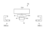
続いて、第1の上側処理ブロックD22、第2の上側処理ブロックD32に設けられるシャトルについて、夫々7A、7Bとして説明する。シャトル7Aは、移動機構72Aと、移動体73Aと、支持体74Aと、を備えている。移動機構72Aは左右に伸びる長尺な部材として構成されると共に、既述した第1の上側処理ブロックD22のスペース71Aに収まるように設けられている。移動体73Aは移動機構72Aに対して前方側に接続されており、左右に伸長している。支持体74Aは移動体73Aに対して前方側に接続されており、左右に細長の直方体状に形成されている。この支持体74A上にウエハWが支持されて、水平な直線状且つ左右方向に沿って搬送される。
Next, the shuttles provided in the first upper processing block D22 and the second upper processing block D32 will be described as 7A and 7B, respectively. The
移動機構72Aにより、移動体73Aが当該移動機構72Aに対して左右に移動自在である。そして、この移動機構72Aに対する移動体73Aの移動に応じて、移動体73Aに対して支持体74Aが左右に移動する(図6~図8参照)。移動体73Aは、その右端が移動機構72Aの右端よりも右側(インターフェイスブロックD4側)に位置する右位置と、その左端が移動機構72Aの左端よりも左側(キャリアブロックD1側)に位置する左位置と、の間で移動する。移動体73Aが上記の右位置に位置するとき、支持体74Aの右端が移動体73Aの右端よりも右側に位置する状態(図6に示す状態)となる。当該状態の支持体74Aの位置を右搬送位置とする。移動体73Aが上記の左位置に位置するとき、支持体74Aの左端が移動体73Aの左端よりも左側に位置する状態(図8に示す状態)となる。当該状態の支持体74Aの位置を左搬送位置とする。
The moving
シャトル7Aは、第2の上側処理ブロックD32に設けられるTRS11から第1の上側処理ブロックD22に設けられるTRS12(第4の載置部)に向けてウエハWを搬送する。TRS11は、平面視左側が開放される凹部をなすように形成された載置部本体をなす支持板75と、当該支持板75から上側に突出する3本のピン76と、支持板75を昇降させる昇降機構(不図示)と、を備え、例えば第2の上側処理ブロックD32の左端部に位置する。昇降機構は、例えばシリンダーやモーター等のアクチュエータでよく、各支持板75の裏側(下側)に接続され、移動体73Aや支持体74Aの移動軌道と干渉しない位置に設けられている。支持板75の昇降により、ピン76は上昇位置と下降位置との間で移動し、ウエハWの下面を支持する。上記の右搬送位置における支持体74Aの右端部は、平面視、支持板75がなす上記の凹部に収まった状態となり、ピン76の昇降により、支持体74AとTRS11との間でウエハWを受け渡すことができる。
The
TRS12については、支持板75が平面視右側が開放される凹部をなすように形成されることを除き、TRS11と同様の構成である。そして、上記の左搬送位置における支持体74Aの左端部は、平面視、支持板75がなす上記の凹部に収まった状態となり、支持体74AとTRS12との間でウエハWを受け渡すことができる。TRS12は、キャリアブロックD1の搬送機構33との間でもウエハWを受け渡せるように、第1の上側処理ブロックD22の左端部に設けられる。支持体74に支持された基板(ウエハW)の搬送は、前に述べたことから、移動体73Aと支持体74Aのように前後方向に設けられた複数の部材が、互いの相対的な左右方向の位置を変えながら行われると言える。そのように基板が搬送されることで、支持体74Aに対して左右方向夫々に位置するTRS11、TRS12は移動体73Aと干渉し難くなり、基板を容易に支持可能な3箇所以上の位置にピン76を配置することが可能になっている。
TRS12 has the same configuration as TRS11, except that the
第2のバイパス搬送機構であるシャトル7Bについては、シャトル7Aとは異なる高さに設けられ、例えばシャトル7Aよりも下方に位置している。シャトル7Bは、シャトル7Aと同様に構成されており、シャトル7Bの構成部材である移動機構、移動体、支持体の各符号は、シャトル7Aの構成部材と区別するために、数字の後のAの代わりにBを付して示す。具体的には、例えばシャトル7Bの移動機構は72Bとして示す。そして、この移動機構72Bは、第2の上側処理ブロックD32のスペース71Bに収まるように設けられる。
シャトル7Bは、第2の上側処理ブロックD32に設けられるTRS13から第1の上側処理ブロックD22に設けられるTRS14に向けてウエハWを搬送する。TRS13はTRS11と同様の構成であり、インターフェイスブロックD4との間でもウエハWを受け渡せるように、第2の上側処理ブロックD32の右端部に設けられている。TRS14はTRS12と同様の構成であり、搬送機構6Bとの間でウエハWの受け渡しが行えるようにモジュール積層体T2よりも左側に設けられており、TRS12よりは右側に位置する。
上記のようにシャトル7Bはシャトル7Aの下方に設けられているので、第2のバイパス用基板載置部であるTRS13及びTRS14が位置する高さは、第1のバイパス用基板載置部であるTRS11及びTRS12が位置する高さよりも低い。つまり、図2に示すように、シャトル7A、TRS11及びTRS12の組、シャトル7B、TRS13、TRS14の組は、縦方向(垂直方向)において互いにずれた位置に設けられている。
As described above,
そして、シャトル7AによるウエハWの搬送路(第1のバイパス搬送路)、シャトル7BによるウエハWの搬送路(第2のバイパス搬送路)を夫々77A、77Bとすると、これらの搬送路77A、77Bの前後の位置は互いに同じである。既述のTRS11~TRS14の位置に対応して、搬送路77Aは第2の上側処理ブロックD22へ突出すると共に、搬送路77Bは第1の上側処理ブロックD22へ突出している。そのように突出することで搬送路77Aの右側と搬送路77Bの左側とが平面視、互いに重なっている。なお搬送路77A、77Bは、例えば平面視、加熱モジュール54の熱板55から外れ、冷却プレート56の待機位置と重なる位置としてもよい。そのように熱板55から比較的離れて搬送路を配置することで、搬送されるウエハWが熱の影響を受けることを、より確実に抑えることができる。
Then, the transport path (first bypass transport path) of the wafer W by the
シャトル7AによるウエハWの搬送について、図6~図8を参照しながら順を追って説明する。第2の上側処理ブロックD32の搬送機構6Dは、を第2の上側処理ブロックD32内の各処理モジュールで処理されたウエハWを、TRS11の上昇位置におけるピン76上に受け渡す。ピン76が下降位置へと移動し、既述の右搬送位置における支持体74AにウエハWが受け渡される(図6)。移動体73A及び支持体74Aが各々左側へ移動する一方で、TRS11のピン76は上昇位置に戻る(図7)。
The transfer of the wafer W by the
支持体74Aが既述の左搬送位置に移動すると、TRS12の下降位置におけるピン76が上昇位置に移動してウエハWを支持する(図8)。支持体74Aが右搬送位置へ向けて移動すると、ピン76が下降位置に戻る。以降は、キャリアブロックD1の搬送機構33がウエハWを受け取る。このように、シャトル7Aは下流側のブロックであるキャリアブロックD1に向けてウエハWを搬送する。シャトル7B、TRS13、TRS14についてもシャトル7A、TRS11、TRS12と夫々同様に動作し、TRS13からTRS14へウエハWが搬送される。つまり、シャトル7Bは下流側のブロックである第1の上側処理ブロックD22に向けてウエハWを搬送する。
When
また、塗布、現像装置1は、制御部10を備えている(図1参照)。この制御部10はコンピュータにより構成されており、プログラム、メモリ、CPUを備えている。プログラムには、塗布、現像装置1における一連の動作を実施することができるようにステップ群が組み込まれている。そして、当該プログラムによって制御部10は塗布、現像装置1の各部に制御信号を出力し、当該各部の動作が制御される。具体的に搬送機構6A~6D、シャトル7A、7B、各処理モジュールの動作が制御される。それにより、後述のウエハWの搬送、ウエハWの処理、ウエハWの異常判定が行われる。上記のプログラムは、例えばコンパクトディスク、ハードディスク、DVDなどの記憶媒体に格納されて、制御部10にインストールされる。
The coating and developing
続いて、塗布、現像装置1におけるウエハWの処理及び搬送経路について、既述した往路、復路を夫々示す図9、図10を参照して説明する。図9、図10では、モジュール間でのウエハWの搬送を表す一部の矢印上あるいは矢印の近傍に、当該搬送に用いる搬送機構を表示している。
Next, the processing and transport path of the wafer W in the coating and developing
先ず、支持台12の移動ステージ15に載置されたキャリアCから、搬送機構32によりウエハWが搬出される。そして、当該搬送機構32によりウエハWは処理前検査モジュール41に搬送され、画像データが取得されて異常の有無が判定される。
First, the wafer W is removed by the
その後、ウエハWは搬送機構32によりTRS1に搬送される。然る後、当該ウエハWは搬送機構33により疎水化処理モジュール30、SCPL1の順に搬送された後、搬送機構6Aにより第1の下側処理ブロックD21に取り込まれ、反射防止膜形成モジュール47→加熱モジュール54の順で搬送されることで、反射防止膜が形成される。その後、ウエハWはモジュール積層体T2のSCPL4に搬送され、搬送機構6Cにより、レジスト膜形成モジュール49→加熱モジュール54の順で搬送されることで、レジスト膜が形成される。その後、ウエハWはモジュール積層体T3のTRS5に搬送される。
Then, the wafer W is transferred to TRS1 by the
然る後、ウエハWは前方側の搬送機構36により裏面洗浄モジュール65、ICPLを経由して、搬送機構38により露光機20に搬送され、所定のパターンに沿って当該ウエハWの表面のレジスト膜が露光される。露光後のウエハWは、搬送機構38によりTRS6に搬送され、その後、後方側の搬送機構37により、露光後洗浄モジュール66に搬送される。
Then, the wafer W is transported by the
その後のウエハWの搬送経路は、上記したように第1の上側処理ブロックD22で処理を行う経路(第1の経路とする)と、第2の上側処理ブロックD32で処理を行う経路(第2の経路とする)と、に分かれる。第2の経路について説明すると、搬送機構37はモジュール積層体T3のTRS7にウエハWを搬送し、搬送機構6Dによって当該ウエハWが第2の上側処理ブロックD32に取り込まれる。そしてウエハWは、加熱モジュール54→SCPL3→現像モジュール51→処理後検査モジュール57の順で搬送されることで、レジストパターンが形成された後に画像データが取得されて、異常の有無が判定される。
The wafer W is then transported through a path that undergoes processing in the first upper processing block D22 (referred to as the first path) and a path that undergoes processing in the second upper processing block D32 (referred to as the second path) as described above. Regarding the second path, the
その後、ウエハWは図6~図8で説明したように搬送機構6D→TRS11→シャトル7A→TRS12の順で搬送された後、キャリアブロックD1の搬送機構33が当該ウエハWを受け取り、TRS2に搬送する。このようにバイパス搬送路形成ブロックである第1の上側処理ブロックD22及び第2の上側処理ブロックD22の主搬送機構である搬送機構6B,6Dのうち6Dと、シャトル7Aと、によってウエハWが下流側のブロックへ向けて搬送される。その後、ウエハWは搬送機構32により、支持台13の移動ステージ15上のキャリアCに格納される。
Then, as explained in Figures 6 to 8, the wafer W is transported in the order of
続いて上記の第1の経路について説明すると、ウエハWは搬送機構37→TRS13→シャトル7B→TRS14→搬送機構6Bの順で搬送されて、第1の上側処理ブロックD22にウエハWが取り込まれる。そして、当該ウエハWは搬送機構6Bにより、加熱モジュール54→SCPL2→現像モジュール51→処理後検査モジュール57の順で搬送され、第2の経路のウエハWと同様に処理を受けた後、キャリアブロックD1のTRS3に搬送される。このようにバイパス搬送路形成ブロックである第1の上側処理ブロックD22及び第2の上側処理ブロックD22の主搬送機構である搬送機構6B,6Dのうち6Bと、シャトル7Bと、によってウエハWが下流側のブロックへ向けて搬送される。続いてウエハWは、搬送機構33によりTRS2に搬送され、以降は第2の経路のウエハWと同様、搬送機構32により支持台13の移動ステージ15上のキャリアCへ搬送される。
Next, regarding the first path, the wafer W is transported in the order of the
以上に述べたように、塗布、現像装置1におけるキャリアブロックD1については、キャリアC、下側処理ブロック(一の処理ブロック)G1、上側処理ブロック(他の処理ブロック)G2に対してウエハWを各々受け渡すためのTRS、SCPLを含むモジュール積層体T1が設けられる。そして、搬送機構32、33が夫々設けられ、搬送機構32がキャリアCに対する受け渡しを、搬送機構33がモジュール積層体T1のモジュール間での受け渡しを夫々受け持つ。このように搬送機構32と搬送機構33との役割が分かれることで、搬送機構32はキャリアCに対するウエハWの搬入出を速やかに行うことができる。一方で、搬送機構33を介してウエハWが搬送される下側処理ブロックG1及び上側処理ブロックG2をなす各処理ブロックD21、D22、D31、D32においては処理モジュールが積層され、各々の処理モジュールでウエハWを処理可能である。従って塗布、現像装置1によれば、高いスループットを得ることができる。さらに、キャリアCに対してウエハWを受け渡す搬送口24が臨む搬送領域31が前後に伸び、この搬送領域31において搬送機構32、33がモジュール積層体T1の前方、後方に夫々設けられることにより、キャリアブロックD1の左右の幅を比較的小さくすることができる。従って、塗布、現像装置1によれば、フットプリント(占有床面積)を小さくすることができる。
As described above, the carrier block D1 in the coating and developing
そして、キャリアブロックD1には処理前検査モジュール41が設けられている。この処理前検査モジュール41は、モジュール積層体T1に右端部が重なると共に筐体11の側壁を貫くことで、その左端部が搬送領域31から突出している。つまり、上記のモジュール積層体T1を配置することによって搬送領域31の前後の中央に形成されるスペース及びキャリアCの移載を行う筐体11の外側のスペースを利用して、処理前検査モジュール41が配置されている。即ち、処理前検査モジュール41をキャリアブロックD1に設置しつつ、当該キャリアブロックD1のフットプリントの増大が防止されている。
The carrier block D1 is provided with a
さらに搬送機構33の後方側に処理モジュールとして疎水化処理モジュール30を配置し、搬送機構33によりアクセスされるようにしている。この疎水化処理モジュール30の配置によっても、塗布、現像装置1の左右の幅の拡大が防止されている。そして搬送機構33が疎水化処理モジュール30に対して、搬送機構32が処理前検査モジュール41に対して、夫々ウエハWを受け渡す。それにより搬送機構32、33間での負荷の偏りが抑制され、これらの処理モジュールを設けることによるスループットの低下が防止されている。ただし、搬送機構33により、処理前検査モジュール41にウエハWが受け渡される構成としてもよい。
Furthermore, a
また、ウエハWの搬入出用にキャリアCが載置される移動ステージ15を複数設けるにあたり、モジュール積層体T1に対して前方側に複数段に設けている。このようにモジュール積層体T1の前方側に移動ステージ15が集約されるように配置されることで、十分なスループットを確保するために必要な数の移動ステージ15の設置を可能にしつつ、搬送領域31の前後の中央部を当該モジュール積層体T1及び処理前検査モジュール41の設置領域とすることができる。そして、そのようにモジュール積層体T1を配置することで、その後方に搬送機構33を配置することができる。従って、既述したように各移動ステージ15をモジュール積層体T1に対して前方側、且つ互いに異なる高さに設けることは、スループットを高くしつつ、装置のフットプリントを低減させることに寄与することになる。
Furthermore, when providing multiple
ところで、キャリア用の仮置き部である仮置きステージ16を設けることで不要なキャリアCを移動ステージ15から退避させることができるので、キャリアCに対するウエハWの搬入出を効率良く行うことができる。キャリアブロックD1では、その仮置きステージ16については、前後方向においてモジュール積層体T1と同じ位置、及び当該モジュール積層体T1に対して後方の位置に設けられている。つまり、既述したレイアウトで移動ステージ15を設けることで、搬送機構32によるアクセスが行われない空いたスペースを利用して仮置きステージ16が設けられていることになる。即ち、仮置きステージ16は、キャリアブロックD1の大型化が防止されるレイアウトで配置されている。
By providing the
さらに塗布、現像装置1によればシャトル7A、7Bが設けられ、これらのシャトル7A、7Bにより、キャリアブロックD1へ向けてウエハWが搬送される。それにより第1の上側処理ブロックD22及び第2の上側処理ブロックD32のうち、一方のブロックで処理が行われるウエハWについて、他方のブロックの処理モジュールがバイパスされるようにキャリアブロックD1に向けて搬送される。従って、第1の上側処理ブロックD22の搬送機構6B及び第2の上側処理ブロックD32の搬送機構6Dの負荷(より詳しくはブロック内で必要な搬送工程の数)が低減される。結果として、塗布、現像装置1におけるスループットを、より向上させることができる。
Furthermore, the coating and developing
ところでキャリアブロックD1の筐体11の上部、第1及び第2の処理ブロックD2、D3の各筐体の上部、インターフェイスブロックD4の筐体の上部には、図示しない気流形成ユニットが設けられる。各気流形成ユニットは、塗布、現像装置1の外側の空気を取り込んで当該気流形成ユニットが設けられるブロックにおけるウエハWの搬送路に供給して、気流を形成する。図11には、キャリアブロックD1、第2の処理ブロックD22の気流形成ユニットを夫々81、82として示している。図示の便宜上、これらの気流形成ユニット81、82はキャリアブロックD1、第1の処理ブロックD2から夫々離れた位置に表示している。
By the way, airflow forming units (not shown) are provided on the top of the
気流形成ユニット82は図示しないダクトを介して、第1の処理ブロックD2をなす第1の下側処理ブロックD21、第1の上側処理ブロックD22の各搬送領域53の天井部に設けられるフィルタに空気を供給する。当該フィルタから供給された空気は搬送領域53を下方に向かい、図示しない第1の下側処理ブロックD21、第1の上側処理ブロックD22の下部側に設けられる図示しない排気口から排気される。
The
例えばキャリアブロックD1においては、例えば図11に示すように搬送領域31の前方側の端部に縦長に形成されたフィルタ83が設けられる。そして、気流形成ユニット81からフィルタ83に供給された空気は、当該フィルタ83から搬送領域31の後方に向けて供給される。モジュール積層体T1よりも後方における例えばブロックの底部には排気孔84が開口しており、フィルタ83から供給された空気が当該排気孔84から排気される。
For example, in carrier block D1, as shown in FIG. 11, a vertically
各ブロックにおける空気の供給量及び排気量のバランスが調整されることにより、第1の下側処理ブロックD21、第1の上側処理ブロックD22の方が、搬送領域31よりも圧力が高い状態とされる。それにより、上記のように搬送領域53に供給される空気の一部が搬送領域31に流れ込み、排気孔84から排気される。図11は、このように搬送領域31、53に形成される気流を矢印で示している。このように形成される気流により、疎水化処理モジュール30で使用する処理ガスが、搬送領域31に流入することがより確実に防止される。仮に、当該処理ガスが搬送領域31を介して現像モジュール51に流入して現像液と反応すると現像欠陥を発生させるおそれがあるが、上記の気流の形成により、そのような欠陥の発生が防止されることになる。即ち、当該気流の形成により、ウエハWから製造される製品の歩留りの低下が防止される。なおフィルタ83、気流形成ユニット81、82は、気流形成機構をなす。
By adjusting the balance of the air supply amount and exhaust amount in each block, the first lower processing block D21 and the first upper processing block D22 are made to have a higher pressure than the
ところで既述の処理前検査モジュール41が設けられる位置に、当該処理前検査モジュール41の代わりに処理後検査モジュール57を設けてもよい。その場合には、図9で述べた往路については、検査モジュールへの搬送が行われない経路とすればよい。具体的にはウエハWをキャリアC→搬送機構32→TRS1→搬送機構33→SCPL1の順で搬送して、第1の下側処理ブロックD21に搬入すればよい。そして図10で述べた復路については、そのようにキャリアブロックD1に設けた処理後検査モジュール57を経由するものとすればよい。具体的には、処理を終えてキャリアブロックD1のTRS2に搬送されたウエハWを、搬送機構32は処理後検査モジュール57に搬送した後にキャリアCに戻すようにすればよい。
However, instead of the
そのようにキャリアブロックD1に処理後検査モジュール57を配置した場合は、処理前検査モジュール41は、例えば第1の下側処理ブロックD21の後部側処理部50を構成する処理モジュールとして設けてもよい。なお、キャリアブロックD1に、処理前検査モジュール41及び処理後検査モジュール57のいずれも設けられない構成であってもよく、その場合にもモジュール積層体T1の各モジュールを利用して搬送機構32、33間でウエハWを受け渡して適宜、搬送を行えばよい。
When the
上記の搬送例では、ウエハWを搬出するためにキャリアCを載置する移動ステージ15(ローダー)と、ウエハWを搬入するためにキャリアCを載置する移動ステージ15(アンローダー)とが異なる。ただし一つの移動ステージ15が、ローダーとアンローダーとを兼用してもよい。上記の搬送機構32は4つの移動ステージ15に共用される構成であるため、このように移動ステージ15の用途の切替えを容易に行うことができる利点が有る。
In the above transfer example, the moving stage 15 (loader) on which the carrier C is placed to unload the wafer W is different from the moving stage 15 (unloader) on which the carrier C is placed to load the wafer W. However, one moving
なお、塗布、現像装置1において、上側処理ブロックG2をウエハWの往路、下側処理ブロックG1をウエハWの復路としてもよい。具体的には、例えば装置内で反射防止膜の形成は行わず、第1の上側処理ブロックD22、第2の上側処理ブロックD32の液処理モジュールとして、各々レジスト膜形成モジュール49を設ける。そして第1の下側処理ブロックD21、第2の下側処理ブロックD31の液処理モジュールとして、現像モジュール51を各々設置する。そして既述した搬送経路とは逆の搬送経路でブロック間においてウエハWを搬送することで、レジスト膜の形成、露光、現像を順に行い、レジストパターンを形成するようにしてもよい。従って、シャトルとしては復路を形成することに限られないし、キャリアブロックD1についても復路をなすシャトル用のTRSにウエハWを受け渡す構成であることには限られない。また、シャトルについては第1の下側処理ブロックD21、第2の下側処理ブロックD31に設けてもよい。例えばこれら第1の下側処理ブロックD21、第2の下側処理ブロックD31の液処理モジュールが共にレジスト膜形成モジュール49であり、シャトルを用いていずれか一方のブロックのレジスト膜形成モジュール49でウエハWが処理されるように装置を構成することもできる。
In addition, in the coating and developing
また、装置で行う液処理としては上記した例に限られず、薬液の塗布による絶縁膜の形成や、薬液の塗布によるレジスト膜の表面を保護するための保護膜の形成や、ウエハWを互いに貼り合わせるための接着剤の塗布処理などが含まれていてもよい。また、ウエハWの表面あるいは裏面に洗浄液を供給する洗浄処理を行ってもよい。従って、本技術の基板処理装置としては塗布、現像装置であることには限られない。 In addition, the liquid processing performed by the apparatus is not limited to the above examples, and may include forming an insulating film by applying a chemical liquid, forming a protective film to protect the surface of a resist film by applying a chemical liquid, and applying an adhesive to bond wafers W to each other. A cleaning process may also be performed in which a cleaning liquid is supplied to the front or back surface of the wafer W. Therefore, the substrate processing apparatus of this technology is not limited to a coating and developing apparatus.
さらに下側処理ブロックG1、上側処理ブロックG2としては、インターフェイスブロックD4により互いに接続されていなくてもよい。図12の基板処理装置8の概略図を参照して説明する。モジュール積層体T1にはTRS21~TRS23が含まれるとする。TRS21がキャリアCに対する受け渡し用で、搬送機構32によりキャリアC-TRS21間でウエハWが搬送される。TRS22、TRS23が下側処理ブロックG1、上側処理ブロックG2に対する受け渡し用で、TRS21-TRS22間、TRS21-TRS23間でウエハWが夫々搬送機構33により搬送される。キャリアCからTRS21を経由してTRS22、TRS23から下側処理ブロックG1、上側処理ブロックG2に夫々搬入されたウエハWは、処理後にTRS22、TRS23からTRS21を経由してキャリアCに戻される。つまり、下側処理ブロックG1及び上側処理ブロックG2の一方でのみウエハWは処理を受けて、キャリアCに戻されるように装置が構成されていてもよい。
Furthermore, the lower processing block G1 and the upper processing block G2 do not have to be connected to each other by the interface block D4. The description will be made with reference to the schematic diagram of the
また、下側処理ブロックG1、上側処理ブロックG2の各々は左右に並ぶ2つの処理ブロックにより構成することに限られず、1つの処理ブロックにより構成されていてもよい。また、下側処理ブロックG1、上側処理ブロックG2の各々は3つ以上の左右に並んだ複数の処理ブロックにより構成され、左右に並ぶ処理ブロック間でウエハWが搬送されるようにしてもよい。 Furthermore, each of the lower processing block G1 and the upper processing block G2 is not limited to being composed of two processing blocks arranged side by side, but may be composed of one processing block. Furthermore, each of the lower processing block G1 and the upper processing block G2 may be composed of three or more processing blocks arranged side by side, and the wafer W may be transported between the processing blocks arranged side by side.
なお各処理ブロックにおいて、液処理モジュールが前方、後部側処理部50をなす処理モジュールが後方に位置するが、このレイアウトは前後逆であってもよい。また、キャリアブロックD1においても搬送機構32、33やキャリアC用の各ステージ等のレイアウトは前後逆であってもよい。また、キャリアブロックD1と、他のブロックの並びも左右逆であってもよい。
In each processing block, the liquid processing module is located at the front and the processing module constituting the
そしてキャリアブロックD1においては、疎水化処理モジュール30の代りに、処理後検査モジュール57などの他のモジュールを設け、搬送機構33により搬送が行われるようにしてもよい。ただし、疎水化処理モジュール30は処理を行うにあたり、ウエハWを載置する載置部(熱板)を横方向に移動させなくてよい。つまり、搬送機構33の後方に処理モジュールを設けるにあたり、そのようにウエハWの載置部を横方向に移動させずに処理を行う処理モジュールを設けることが、キャリアブロックD1の大型化、ひいては基板処理装置の大型化を防ぐために好ましい。なお、モジュール積層体T1を構成するTRS、SCPLの順番は装置内においてウエハWを搬送可能な範囲で、適宜高さを変更したり、重ねられる順番を入れ替えたりしてもよい。
In the carrier block D1, other modules such as a
また、疎水化処理モジュール30は、モジュール積層体T1をなすTRS、SCPLに重なるように配置してもよい。ただし、モジュール積層体T1に多数のTRS、SCPLを配置してウエハWを載置することで、キャリアブロックD1と第1の処理ブロックD2間、及びキャリアCとキャリアブロックD1との間でのウエハWの受け渡しが速やかに行われるようにすることができる。従って、疎水化処理モジュール30は既述したように搬送領域31の後方側に配置することが好ましい。さらに塗布、現像装置1において、処理前検査モジュール41に搬送機構32によりウエハWを搬送した後、搬送機構33が当該検査モジュール41にてウエハWを受け取り、SCPL1に搬送し、下側処理ブロックD21にウエハWが取込まれるようにしてもよい。つまり、搬送機構32、33間でのウエハWの受け渡しは、仮置きモジュールにて行うことには限られない。
The
そして、今回開示された実施形態は、全ての点で例示であって制限的なものではないと考えられるべきである。上記の実施形態は、添付の特許請求の範囲及びその趣旨を逸脱することなく、様々な形態で省略、置換、変更及び組み合わせがなされてもよい。 The embodiments disclosed herein should be considered in all respects as illustrative and not restrictive. The above-described embodiments may be omitted, substituted, modified, and combined in various forms without departing from the scope and spirit of the appended claims.
C キャリア
D2 第1の処理ブロック
D21 第1の下側処理ブロック
D22 第1の上側処理ブロック
15 移動ステージ
TRS 受け渡しモジュール
T1 モジュール積層体
W ウエハ
31 搬送領域
32、33 搬送機構
6A、6B、6C、6D 搬送機構
C carrier D2 first processing block D21 first lower processing block D22 first
Claims (15)
前記基板を各々処理し、互いに積層されて設けられる複数の処理モジュールと、前記複数の処理モジュールに共用されて前記基板を搬送する主搬送機構と、を備え、前記キャリア載置部に対して平面視、左右の一方に設けられる一の処理ブロックと、
前記基板を各々処理し、互いに積層されて設けられる複数の処理モジュールと、前記複数の処理モジュールに共用されて前記基板を搬送する主搬送機構と、を備え、前記一の処理ブロックに対して縦方向に重なる他の処理ブロックと、
平面視、前記キャリア載置部と、前記一の処理ブロック及び前記他の処理ブロックとの間に介在するように、前記キャリアブロックに設けられる前記基板の搬送領域と、
前記キャリアに対して前記基板を受け渡すために前記搬送領域に設けられる第1の搬送機構と、
前記第1の搬送機構、前記一の処理ブロックの主搬送機構、前記他の処理ブロックの主搬送機構によって夫々前記基板が受け渡される第1の載置部、第2の載置部、第3の載置部が互いに縦方向に重なって構成されると共に、平面視、前記第1の搬送機構に対して前後の一方側に設けられる載置部の積層体と、
平面視、前記第1の搬送機構と共に前記積層体を前後から挟むように前記搬送領域に設けられ、前記第1の載置部と前記第2の載置部との間、前記第1の載置部と前記第3の載置部との間で夫々前記基板を搬送するための第2の搬送機構と、
を備える基板処理装置。 a carrier block including a carrier placement portion on which a carrier for storing a substrate is placed;
a processing block including a plurality of processing modules each for processing the substrate, the processing block being stacked on top of one another, and a main transport mechanism shared by the plurality of processing modules for transporting the substrate, the processing block being provided on either the left or right side of the carrier placement unit in a plan view;
a plurality of processing modules each for processing the substrate, the processing modules being stacked on top of one another; and a main transport mechanism shared by the plurality of processing modules for transporting the substrate, the main transport mechanism being overlapped in a vertical direction with respect to the first processing block;
a transport region for the substrate provided in the carrier block so as to be interposed between the carrier placement part, the first processing block, and the second processing block in a plan view;
a first transport mechanism provided in the transport region for transferring the substrate to the carrier;
a stack of platform parts, which are configured so that a first platform part, a second platform part, and a third platform part to which the substrate is transferred by the first transport mechanism, the main transport mechanism of the one processing block, and the main transport mechanism of the other processing block, are stacked one on top of the other in the vertical direction, and which are provided on one of the front and rear sides of the first transport mechanism in a plan view;
a second transport mechanism that is provided in the transport region so as to sandwich the stack from the front and rear together with the first transport mechanism in a plan view, and that transports the substrate between the first placement part and the second placement part and between the first placement part and the third placement part, respectively;
A substrate processing apparatus comprising:
平面視で前記積層体に重なる位置に、前記第1の搬送機構または第2の搬送機構により前記基板が受け渡される第3の処理モジュールが設けられる請求項1記載の基板処理装置。 The processing module of the one processing block and the processing module of the other processing block are respectively referred to as a first processing module and a second processing module.
The substrate processing apparatus according to claim 1 , further comprising a third processing module to which the substrate is transferred by the first transport mechanism or the second transport mechanism, the third processing module being disposed at a position overlapping the stack in a plan view.
前記第3の処理モジュールには前記第1の搬送機構により前記基板が受け渡される請求項2ないし5のいずれか一つに記載の基板処理装置。 a fourth processing module to which the substrate is transferred by the second transfer mechanism is provided at one of the front and rear sides of the second transfer mechanism;
6. The substrate processing apparatus according to claim 2, wherein the substrate is transferred to the third processing module by the first transfer mechanism.
前記一の処理ブロックの処理モジュール、前記他の処理ブロックの処理モジュールを夫々第1の処理モジュール、第2の処理モジュールとすると、
前記複数の第1の処理モジュールまたは複数の第2の処理モジュールには、前記基板に塗布液を供給して塗布膜を形成する塗布膜形成モジュールが含まれ、
前記第4の処理モジュールは、前記塗布液の供給前に前記基板をガス処理して疎水化する疎水化処理モジュールである請求項1ないし6のいずれか一つに記載の基板処理装置。 a fourth processing module to which the substrate is transferred by the second transfer mechanism is provided at one of the front and rear sides of the second transfer mechanism;
The processing module of the one processing block and the processing module of the other processing block are respectively referred to as a first processing module and a second processing module.
the plurality of first processing modules or the plurality of second processing modules includes a coating film forming module that supplies a coating liquid to the substrate to form a coating film;
7. The substrate processing apparatus according to claim 1, wherein the fourth processing module is a hydrophobization processing module which performs a gas processing on the substrate to hydrophobize the substrate before the coating liquid is supplied.
前後において前記積層体と同じ位置かあるいは当該積層体に対して前後の一方側に設けられる、前記キャリアを仮置きするためのキャリア用の仮置き部と、
前記仮置き部と、前記キャリア載置部との間で前記キャリアを移載するキャリア移載機構と、を備える請求項9記載の基板処理装置。 On one of the left and right sides of the transport area,
a temporary placement portion for a carrier, the temporary placement portion being provided at the same position as the stack in the front and rear or on one side of the stack in the front and rear;
The substrate processing apparatus according to claim 9 , further comprising: a carrier transfer mechanism that transfers the carrier between the temporary placement unit and the carrier placement unit.
前記基板は前記キャリアブロックから前記一の処理ブロックを経由して前記中継ブロックへ向う往路と、前記中継ブロックから前記他の処理ブロックを経由して前記キャリアブロックへ向う復路と、を搬送される請求項1ないし10のいずれか一つに記載の基板処理装置。 a relay block including a lifting and lowering mechanism for transporting the substrate between the first processing block and the second processing block is connected to one of the left and right sides of the first processing block and the second processing block;
11. A substrate processing apparatus as described in any one of claims 1 to 10, wherein the substrate is transported on an outward route from the carrier block via the one processing block to the relay block, and on a return route from the relay block to the carrier block via the other processing block.
前記第3の搬送機構は、前記処理モジュールを経由せずに前記基板を下流側のブロックへ向けて搬送するために、前記左側の処理ブロック、前記右側の処理ブロックの各々に設けられる請求項12記載の基板処理装置。 at least one of the one processing block and the other processing block includes the plurality of stacked processing modules and the main transport mechanism, and is configured with a left processing block and a right processing block arranged side by side,
The substrate processing apparatus according to claim 12 , wherein the third transport mechanism is provided in each of the left processing block and the right processing block to transport the substrate toward a downstream block without passing through the processing module.
前記基板を各々処理し、互いに積層されて設けられる複数の処理モジュールと、前記複数の処理モジュールに共用されて前記基板を搬送する主搬送機構と、を備え、前記キャリア載置部に対して平面視、左右の一方に設けられる一の処理ブロックにて前記基板を搬送する工程と、
前記基板を各々処理し、互いに積層されて設けられる複数の処理モジュールと、前記複数の処理モジュールに共用されて前記基板を搬送する主搬送機構と、を備え、前記一の処理ブロックに対して縦方向に重なる他の処理ブロックにて前記基板を搬送する工程と、
平面視、前記キャリア載置部と、前記一の処理ブロック及び前記他の処理ブロックとの間に介在するように前記キャリアブロックに設けられた前記基板の搬送領域に設けられる第1の搬送機構により、前記キャリアに対して前記基板を受け渡す工程と、
互いに縦方向に重なって構成されると共に、平面視、前記第1の搬送機構に対して前後の一方側に設けられる載置部の積層体を構成する第1の載置部、第2の載置部、第3の載置部に夫々、前記第1の搬送機構、前記一の処理ブロックの主搬送機構、前記他の処理ブロックの主搬送機構によって前記基板を受け渡す工程と、
平面視、前記第1の搬送機構と共に前記積層体を前後から挟むように前記搬送領域に設けられる第2の搬送機構により、前記第1の載置部と前記第2の載置部の間、前記第1の載置部と前記第3の載置部との間で夫々前記基板を搬送する工程と、
を備える基板処理方法。 placing a carrier for storing substrates on a carrier placement portion provided on a carrier block;
a process for transporting the substrate in a processing block provided on either the left or right side of the carrier placement unit in a plan view, the processing block including a plurality of processing modules stacked on top of each other and each processing the substrate, and a main transport mechanism shared by the plurality of processing modules and transporting the substrate;
a step of transporting the substrate in another processing block that overlaps the first processing block in a vertical direction, the processing block including a plurality of processing modules that process the substrate and are stacked on top of each other and a main transport mechanism that is shared by the plurality of processing modules and transports the substrate;
a step of transferring the substrate to the carrier by a first transport mechanism provided in a substrate transport region provided in the carrier block so as to be interposed between the carrier placement part, the first processing block, and the second processing block in a plan view;
a step of transferring the substrate to a first mounting portion, a second mounting portion, and a third mounting portion which are configured to be stacked on top of each other in the vertical direction and which constitute a stack of mounting portions provided on one of the front and rear sides of the first transport mechanism in a plan view, by the first transport mechanism, a main transport mechanism of the one processing block, and a main transport mechanism of the other processing block, respectively;
a step of transporting the substrate between the first placement part and the second placement part and between the first placement part and the third placement part by a second transport mechanism provided in the transport region so as to sandwich the stack from the front and rear together with the first transport mechanism in a plan view;
A substrate processing method comprising:
前記コンピュータプログラムは、請求項14記載の基板処理方法を実行するようにステップ群が組まれていることを特徴とする記憶媒体。 A storage medium for storing a computer program for use in a substrate processing apparatus,
15. A storage medium, wherein the computer program is a set of steps for executing the substrate processing method according to claim 14.
Priority Applications (6)
| Application Number | Priority Date | Filing Date | Title |
|---|---|---|---|
| JP2020195422A JP7524736B2 (en) | 2020-11-25 | 2020-11-25 | SUBSTRATE PROCESSING APPARATUS, SUBSTRATE PROCESSING METHOD, AND STORAGE MEDIUM |
| CN202111347980.9A CN114551281A (en) | 2020-11-25 | 2021-11-15 | Substrate processing apparatus, substrate processing method, and storage medium |
| KR1020210158595A KR102825180B1 (en) | 2020-11-25 | 2021-11-17 | Substrate processing apparatus, substrate processing method and recording medium |
| JP2024113570A JP7804867B2 (en) | 2020-11-25 | 2024-07-16 | Substrate processing apparatus, substrate processing method, and storage medium |
| KR1020250081854A KR20250105321A (en) | 2020-11-25 | 2025-06-20 | Substrate processing apparatus, substrate processing method and recording medium |
| JP2025265752A JP2026040525A (en) | 2020-11-25 | 2025-12-18 | Substrate processing apparatus, substrate processing method, and storage medium |
Applications Claiming Priority (1)
| Application Number | Priority Date | Filing Date | Title |
|---|---|---|---|
| JP2020195422A JP7524736B2 (en) | 2020-11-25 | 2020-11-25 | SUBSTRATE PROCESSING APPARATUS, SUBSTRATE PROCESSING METHOD, AND STORAGE MEDIUM |
Related Child Applications (1)
| Application Number | Title | Priority Date | Filing Date |
|---|---|---|---|
| JP2024113570A Division JP7804867B2 (en) | 2020-11-25 | 2024-07-16 | Substrate processing apparatus, substrate processing method, and storage medium |
Publications (2)
| Publication Number | Publication Date |
|---|---|
| JP2022083851A JP2022083851A (en) | 2022-06-06 |
| JP7524736B2 true JP7524736B2 (en) | 2024-07-30 |
Family
ID=81668839
Family Applications (3)
| Application Number | Title | Priority Date | Filing Date |
|---|---|---|---|
| JP2020195422A Active JP7524736B2 (en) | 2020-11-25 | 2020-11-25 | SUBSTRATE PROCESSING APPARATUS, SUBSTRATE PROCESSING METHOD, AND STORAGE MEDIUM |
| JP2024113570A Active JP7804867B2 (en) | 2020-11-25 | 2024-07-16 | Substrate processing apparatus, substrate processing method, and storage medium |
| JP2025265752A Pending JP2026040525A (en) | 2020-11-25 | 2025-12-18 | Substrate processing apparatus, substrate processing method, and storage medium |
Family Applications After (2)
| Application Number | Title | Priority Date | Filing Date |
|---|---|---|---|
| JP2024113570A Active JP7804867B2 (en) | 2020-11-25 | 2024-07-16 | Substrate processing apparatus, substrate processing method, and storage medium |
| JP2025265752A Pending JP2026040525A (en) | 2020-11-25 | 2025-12-18 | Substrate processing apparatus, substrate processing method, and storage medium |
Country Status (3)
| Country | Link |
|---|---|
| JP (3) | JP7524736B2 (en) |
| KR (2) | KR102825180B1 (en) |
| CN (1) | CN114551281A (en) |
Families Citing this family (2)
| Publication number | Priority date | Publication date | Assignee | Title |
|---|---|---|---|---|
| JP2025162275A (en) | 2024-04-15 | 2025-10-27 | 東京エレクトロン株式会社 | Substrate processing apparatus and substrate processing method |
| JP2025167466A (en) | 2024-04-26 | 2025-11-07 | 東京エレクトロン株式会社 | Substrate processing apparatus and substrate processing method |
Citations (7)
| Publication number | Priority date | Publication date | Assignee | Title |
|---|---|---|---|---|
| JP2009021440A (en) | 2007-07-12 | 2009-01-29 | Tokyo Electron Ltd | Substrate processing apparatus, substrate processing method, and storage medium |
| JP2010161407A (en) | 2010-03-29 | 2010-07-22 | Tokyo Electron Ltd | Substrate processing system |
| JP2012054469A (en) | 2010-09-02 | 2012-03-15 | Tokyo Electron Ltd | Coating and developing device, coating and developing method and storage medium |
| JP2013069916A (en) | 2011-09-22 | 2013-04-18 | Tokyo Electron Ltd | Substrate processing apparatus and substrate processing method and storage medium |
| JP2015039019A (en) | 2014-10-08 | 2015-02-26 | 株式会社Screenセミコンダクターソリューションズ | Substrate processing equipment |
| US20160351430A1 (en) | 2015-05-29 | 2016-12-01 | Semes Co., Ltd. | Apparatus for processing substrate |
| JP2019004072A (en) | 2017-06-16 | 2019-01-10 | 東京エレクトロン株式会社 | Substrate processing apparatus, substrate processing method, and storage device |
Family Cites Families (2)
| Publication number | Priority date | Publication date | Assignee | Title |
|---|---|---|---|---|
| JP5381592B2 (en) * | 2009-10-06 | 2014-01-08 | 東京エレクトロン株式会社 | Substrate processing equipment |
| JP5880247B2 (en) * | 2012-04-19 | 2016-03-08 | 東京エレクトロン株式会社 | Substrate processing apparatus, substrate processing method, and storage medium |
-
2020
- 2020-11-25 JP JP2020195422A patent/JP7524736B2/en active Active
-
2021
- 2021-11-15 CN CN202111347980.9A patent/CN114551281A/en active Pending
- 2021-11-17 KR KR1020210158595A patent/KR102825180B1/en active Active
-
2024
- 2024-07-16 JP JP2024113570A patent/JP7804867B2/en active Active
-
2025
- 2025-06-20 KR KR1020250081854A patent/KR20250105321A/en active Pending
- 2025-12-18 JP JP2025265752A patent/JP2026040525A/en active Pending
Patent Citations (7)
| Publication number | Priority date | Publication date | Assignee | Title |
|---|---|---|---|---|
| JP2009021440A (en) | 2007-07-12 | 2009-01-29 | Tokyo Electron Ltd | Substrate processing apparatus, substrate processing method, and storage medium |
| JP2010161407A (en) | 2010-03-29 | 2010-07-22 | Tokyo Electron Ltd | Substrate processing system |
| JP2012054469A (en) | 2010-09-02 | 2012-03-15 | Tokyo Electron Ltd | Coating and developing device, coating and developing method and storage medium |
| JP2013069916A (en) | 2011-09-22 | 2013-04-18 | Tokyo Electron Ltd | Substrate processing apparatus and substrate processing method and storage medium |
| JP2015039019A (en) | 2014-10-08 | 2015-02-26 | 株式会社Screenセミコンダクターソリューションズ | Substrate processing equipment |
| US20160351430A1 (en) | 2015-05-29 | 2016-12-01 | Semes Co., Ltd. | Apparatus for processing substrate |
| JP2019004072A (en) | 2017-06-16 | 2019-01-10 | 東京エレクトロン株式会社 | Substrate processing apparatus, substrate processing method, and storage device |
Also Published As
| Publication number | Publication date |
|---|---|
| KR102825180B1 (en) | 2025-06-25 |
| CN114551281A (en) | 2022-05-27 |
| JP2022083851A (en) | 2022-06-06 |
| KR20250105321A (en) | 2025-07-08 |
| JP2026040525A (en) | 2026-03-09 |
| JP2024138513A (en) | 2024-10-08 |
| JP7804867B2 (en) | 2026-01-23 |
| KR20220072762A (en) | 2022-06-02 |
Similar Documents
| Publication | Publication Date | Title |
|---|---|---|
| JP7810229B2 (en) | Substrate processing apparatus and substrate processing method | |
| JP7804867B2 (en) | Substrate processing apparatus, substrate processing method, and storage medium | |
| KR102900238B1 (en) | Substrate processing apparatus and substrate processing method | |
| JP2024128074A (en) | SUBSTRATE PROCESSING APPARATUS AND SUBSTRATE PROCESSING METHOD | |
| JP7211142B2 (en) | SUBSTRATE PROCESSING APPARATUS AND SUBSTRATE PROCESSING METHOD | |
| JP7647857B2 (en) | SUBSTRATE PROCESSING APPARATUS AND SUBSTRATE PROCESSING METHOD | |
| JP7437599B2 (en) | Substrate processing equipment and substrate processing method | |
| JP7771609B2 (en) | Substrate processing apparatus and substrate processing method | |
| TWI913512B (en) | Substrate processing device and substrate processing method | |
| KR20250151995A (en) | Substrate processing apparatus and substrate processing method |
Legal Events
| Date | Code | Title | Description |
|---|---|---|---|
| A621 | Written request for application examination |
Free format text: JAPANESE INTERMEDIATE CODE: A621 Effective date: 20230829 |
|
| A977 | Report on retrieval |
Free format text: JAPANESE INTERMEDIATE CODE: A971007 Effective date: 20240515 |
|
| TRDD | Decision of grant or rejection written | ||
| A01 | Written decision to grant a patent or to grant a registration (utility model) |
Free format text: JAPANESE INTERMEDIATE CODE: A01 Effective date: 20240618 |
|
| A61 | First payment of annual fees (during grant procedure) |
Free format text: JAPANESE INTERMEDIATE CODE: A61 Effective date: 20240701 |
|
| R150 | Certificate of patent or registration of utility model |
Ref document number: 7524736 Country of ref document: JP Free format text: JAPANESE INTERMEDIATE CODE: R150 |