JP7530656B2 - 制御可能なソース/ドレイン構造を有するトランジスタ - Google Patents
制御可能なソース/ドレイン構造を有するトランジスタ Download PDFInfo
- Publication number
- JP7530656B2 JP7530656B2 JP2022117535A JP2022117535A JP7530656B2 JP 7530656 B2 JP7530656 B2 JP 7530656B2 JP 2022117535 A JP2022117535 A JP 2022117535A JP 2022117535 A JP2022117535 A JP 2022117535A JP 7530656 B2 JP7530656 B2 JP 7530656B2
- Authority
- JP
- Japan
- Prior art keywords
- conductive region
- gate
- substrate
- layer
- transistor structure
- Prior art date
- Legal status (The legal status is an assumption and is not a legal conclusion. Google has not performed a legal analysis and makes no representation as to the accuracy of the status listed.)
- Active
Links
Images








Classifications
-
- H—ELECTRICITY
- H10—SEMICONDUCTOR DEVICES; ELECTRIC SOLID-STATE DEVICES NOT OTHERWISE PROVIDED FOR
- H10D—INORGANIC ELECTRIC SEMICONDUCTOR DEVICES
- H10D62/00—Semiconductor bodies, or regions thereof, of devices having potential barriers
- H10D62/10—Shapes, relative sizes or dispositions of the regions of the semiconductor bodies; Shapes of the semiconductor bodies
- H10D62/102—Constructional design considerations for preventing surface leakage or controlling electric field concentration
-
- H—ELECTRICITY
- H10—SEMICONDUCTOR DEVICES; ELECTRIC SOLID-STATE DEVICES NOT OTHERWISE PROVIDED FOR
- H10B—ELECTRONIC MEMORY DEVICES
- H10B12/00—Dynamic random access memory [DRAM] devices
- H10B12/01—Manufacture or treatment
- H10B12/02—Manufacture or treatment for one transistor one-capacitor [1T-1C] memory cells
- H10B12/05—Making the transistor
- H10B12/053—Making the transistor the transistor being at least partially in a trench in the substrate
-
- H—ELECTRICITY
- H10—SEMICONDUCTOR DEVICES; ELECTRIC SOLID-STATE DEVICES NOT OTHERWISE PROVIDED FOR
- H10B—ELECTRONIC MEMORY DEVICES
- H10B12/00—Dynamic random access memory [DRAM] devices
- H10B12/30—DRAM devices comprising one-transistor - one-capacitor [1T-1C] memory cells
- H10B12/34—DRAM devices comprising one-transistor - one-capacitor [1T-1C] memory cells the transistor being at least partially in a trench in the substrate
-
- H—ELECTRICITY
- H10—SEMICONDUCTOR DEVICES; ELECTRIC SOLID-STATE DEVICES NOT OTHERWISE PROVIDED FOR
- H10B—ELECTRONIC MEMORY DEVICES
- H10B12/00—Dynamic random access memory [DRAM] devices
- H10B12/30—DRAM devices comprising one-transistor - one-capacitor [1T-1C] memory cells
- H10B12/48—Data lines or contacts therefor
- H10B12/488—Word lines
-
- H—ELECTRICITY
- H10—SEMICONDUCTOR DEVICES; ELECTRIC SOLID-STATE DEVICES NOT OTHERWISE PROVIDED FOR
- H10D—INORGANIC ELECTRIC SEMICONDUCTOR DEVICES
- H10D30/00—Field-effect transistors [FET]
- H10D30/60—Insulated-gate field-effect transistors [IGFET]
- H10D30/601—Insulated-gate field-effect transistors [IGFET] having lightly-doped drain or source extensions, e.g. LDD IGFETs or DDD IGFETs
- H10D30/608—Insulated-gate field-effect transistors [IGFET] having lightly-doped drain or source extensions, e.g. LDD IGFETs or DDD IGFETs having non-planar bodies, e.g. having recessed gate electrodes
-
- H—ELECTRICITY
- H10—SEMICONDUCTOR DEVICES; ELECTRIC SOLID-STATE DEVICES NOT OTHERWISE PROVIDED FOR
- H10D—INORGANIC ELECTRIC SEMICONDUCTOR DEVICES
- H10D30/00—Field-effect transistors [FET]
- H10D30/60—Insulated-gate field-effect transistors [IGFET]
- H10D30/67—Thin-film transistors [TFT]
- H10D30/6704—Thin-film transistors [TFT] having supplementary regions or layers in the thin films or in the insulated bulk substrates for controlling properties of the device
- H10D30/6713—Thin-film transistors [TFT] having supplementary regions or layers in the thin films or in the insulated bulk substrates for controlling properties of the device characterised by the properties of the source or drain regions, e.g. compositions or sectional shapes
- H10D30/6715—Thin-film transistors [TFT] having supplementary regions or layers in the thin films or in the insulated bulk substrates for controlling properties of the device characterised by the properties of the source or drain regions, e.g. compositions or sectional shapes characterised by the doping profiles, e.g. having lightly-doped source or drain extensions
-
- H—ELECTRICITY
- H10—SEMICONDUCTOR DEVICES; ELECTRIC SOLID-STATE DEVICES NOT OTHERWISE PROVIDED FOR
- H10D—INORGANIC ELECTRIC SEMICONDUCTOR DEVICES
- H10D30/00—Field-effect transistors [FET]
- H10D30/60—Insulated-gate field-effect transistors [IGFET]
- H10D30/67—Thin-film transistors [TFT]
- H10D30/6757—Thin-film transistors [TFT] characterised by the structure of the channel, e.g. transverse or longitudinal shape or doping profile
-
- H—ELECTRICITY
- H10—SEMICONDUCTOR DEVICES; ELECTRIC SOLID-STATE DEVICES NOT OTHERWISE PROVIDED FOR
- H10D—INORGANIC ELECTRIC SEMICONDUCTOR DEVICES
- H10D30/00—Field-effect transistors [FET]
- H10D30/60—Insulated-gate field-effect transistors [IGFET]
- H10D30/751—Insulated-gate field-effect transistors [IGFET] having composition variations in the channel regions
-
- H—ELECTRICITY
- H10—SEMICONDUCTOR DEVICES; ELECTRIC SOLID-STATE DEVICES NOT OTHERWISE PROVIDED FOR
- H10D—INORGANIC ELECTRIC SEMICONDUCTOR DEVICES
- H10D62/00—Semiconductor bodies, or regions thereof, of devices having potential barriers
- H10D62/01—Manufacture or treatment
- H10D62/021—Forming source or drain recesses by etching e.g. recessing by etching and then refilling
-
- H—ELECTRICITY
- H10—SEMICONDUCTOR DEVICES; ELECTRIC SOLID-STATE DEVICES NOT OTHERWISE PROVIDED FOR
- H10D—INORGANIC ELECTRIC SEMICONDUCTOR DEVICES
- H10D62/00—Semiconductor bodies, or regions thereof, of devices having potential barriers
- H10D62/10—Shapes, relative sizes or dispositions of the regions of the semiconductor bodies; Shapes of the semiconductor bodies
- H10D62/17—Semiconductor regions connected to electrodes not carrying current to be rectified, amplified or switched, e.g. channel regions
- H10D62/213—Channel regions of field-effect devices
- H10D62/221—Channel regions of field-effect devices of FETs
- H10D62/235—Channel regions of field-effect devices of FETs of IGFETs
- H10D62/314—Channel regions of field-effect devices of FETs of IGFETs having vertical doping variations
-
- H—ELECTRICITY
- H10—SEMICONDUCTOR DEVICES; ELECTRIC SOLID-STATE DEVICES NOT OTHERWISE PROVIDED FOR
- H10D—INORGANIC ELECTRIC SEMICONDUCTOR DEVICES
- H10D64/00—Electrodes of devices having potential barriers
- H10D64/01—Manufacture or treatment
-
- H—ELECTRICITY
- H10—SEMICONDUCTOR DEVICES; ELECTRIC SOLID-STATE DEVICES NOT OTHERWISE PROVIDED FOR
- H10D—INORGANIC ELECTRIC SEMICONDUCTOR DEVICES
- H10D64/00—Electrodes of devices having potential barriers
- H10D64/01—Manufacture or treatment
- H10D64/025—Manufacture or treatment forming recessed gates, e.g. by using local oxidation
- H10D64/027—Manufacture or treatment forming recessed gates, e.g. by using local oxidation by etching at gate locations
-
- H—ELECTRICITY
- H10—SEMICONDUCTOR DEVICES; ELECTRIC SOLID-STATE DEVICES NOT OTHERWISE PROVIDED FOR
- H10D—INORGANIC ELECTRIC SEMICONDUCTOR DEVICES
- H10D64/00—Electrodes of devices having potential barriers
- H10D64/20—Electrodes characterised by their shapes, relative sizes or dispositions
- H10D64/27—Electrodes not carrying the current to be rectified, amplified, oscillated or switched, e.g. gates
- H10D64/311—Gate electrodes for field-effect devices
- H10D64/411—Gate electrodes for field-effect devices for FETs
- H10D64/511—Gate electrodes for field-effect devices for FETs for IGFETs
- H10D64/512—Disposition of the gate electrodes, e.g. buried gates
-
- H—ELECTRICITY
- H10—SEMICONDUCTOR DEVICES; ELECTRIC SOLID-STATE DEVICES NOT OTHERWISE PROVIDED FOR
- H10D—INORGANIC ELECTRIC SEMICONDUCTOR DEVICES
- H10D64/00—Electrodes of devices having potential barriers
- H10D64/20—Electrodes characterised by their shapes, relative sizes or dispositions
- H10D64/27—Electrodes not carrying the current to be rectified, amplified, oscillated or switched, e.g. gates
- H10D64/311—Gate electrodes for field-effect devices
- H10D64/411—Gate electrodes for field-effect devices for FETs
- H10D64/511—Gate electrodes for field-effect devices for FETs for IGFETs
- H10D64/512—Disposition of the gate electrodes, e.g. buried gates
- H10D64/513—Disposition of the gate electrodes, e.g. buried gates within recesses in the substrate, e.g. trench gates, groove gates or buried gates
-
- H—ELECTRICITY
- H10—SEMICONDUCTOR DEVICES; ELECTRIC SOLID-STATE DEVICES NOT OTHERWISE PROVIDED FOR
- H10D—INORGANIC ELECTRIC SEMICONDUCTOR DEVICES
- H10D30/00—Field-effect transistors [FET]
- H10D30/60—Insulated-gate field-effect transistors [IGFET]
- H10D30/637—Lateral IGFETs having no inversion channels, e.g. buried channel lateral IGFETs, normally-on lateral IGFETs or depletion-mode lateral IGFETs
Landscapes
- Engineering & Computer Science (AREA)
- Manufacturing & Machinery (AREA)
- Insulated Gate Type Field-Effect Transistor (AREA)
- Semiconductor Memories (AREA)
- Electrodes Of Semiconductors (AREA)
- Bipolar Transistors (AREA)
Description
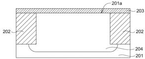
工程S21:初期表面を有する半導体基板を準備する。
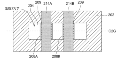
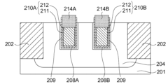
工程S22:半導体基板の初期表面の下にゲート導電領域を形成する。ゲート導電領域210Aを形成することはサブ工程S221~S225を含む。
工程S221:パターニングされた窒化物ハードマスク層を使用して、半導体基板内にゲート凹部を形成する。
工程S222:ゲート凹部内にチャンネル領域を形成する。チャンネル層が(任意的に)半導体基板内のドーピングされた層である。
工程S223:ゲート凹部内にゲート誘電体層を形成する。
工程S224:ゲート凹部内に、ゲート誘電体層により取り囲まれるゲート導電領域を形成する。
工程S225:ゲートキャップ領域を形成する。ならびに、
工程S23:導電領域を形成する。第1の導電領域の底壁がゲート導電領域の上壁に揃えられ、または実質的に揃えられる。導電領域を形成する工程は、サブ工程S231~S233を含む。
工程S231:基板の初期表面を露呈させる。
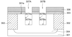
工程S232:露呈された半導体基板をエッチングして、導電領域用凹部を形成する。および、
工程S233:選択的成長法(たとえば、選択的エピタキシ成長(SED)法または原子層堆積(ALD)法)により、導電領域を形成する。
工程S31:初期表面を有する半導体基板を準備する。
工程S32:半導体基板の初期表面の下にゲート導電領域を形成する。ゲート導電領域210Aを形成することはサブ工程S321~S325を含む、
工程S321:パターニングされた窒化物ハードマスク層を使用して、半導体基板内にゲート凹部を形成する。
工程S322:ゲート凹部内にチャンネル領域を形成する。チャンネル層が(任意的に)半導体基板から独立している。
工程S323:ゲート凹部内にゲート誘電体層を形成する。
工程S324:ゲート凹部内に、ゲート誘電体層により取り囲まれるゲート導電領域を形成する。
工程S325:ゲートキャップ領域を形成する。
工程S33:導電領域を形成する。第1の導電領域の底壁がゲート導電領域の上壁に揃えられ、または実質的に揃えられる。導電領域を形成する工程は、サブ工程S331~S333を含む。
工程S331:基板の初期表面を露呈させる。
工程S332:露呈された半導体基板をエッチングして、導電領域用凹部を形成する。および
工程S333:選択的成長法(たとえば、選択的エピタキシ成長(SED)法または原子層堆積(ALD)法)により、第1の導電領域を形成する。
Claims (19)
- 基板、
ゲート導電領域であって、前記ゲート導電領域の少なくとも一部分が前記基板の表面の下に配置されたゲート導電領域、
前記ゲート導電領域の底壁および側壁を取り囲むゲート誘電体層、ならびに
第1の導電領域
を備えており、前記第1の導電領域の底壁が、前記ゲート導電領域の上壁に、揃えられ、または実質的に揃えられており、
前記第1の導電領域の前記底壁から前記第1の導電領域の上壁までのドーピング濃度が調節可能であり、
調節可能な前記ドーピング濃度を有する前記第1の導電領域が、前記基板から独立している、トランジスタ構造。 - 前記第1の導電領域の上壁が、前記第1の導電領域の隣のシャロートレンチアイソレータ(STI)領域の上壁に、揃えられ、または実質的に揃えられているが、前記ゲート導電領域上のゲートキャップ層の上壁よりも低い、請求項1に記載のトランジスタ構造。
- 前記基板がシリコン基板であり、および、調節可能な前記ドーピング濃度を有する前記第1の導電領域が、選択的成長プロセスによって形成されている、請求項1に記載のトランジスタ構造。
- 前記ゲート誘電体層を取り囲むチャンネル層をさらに備えており、前記チャンネル層が前記基板から独立している、請求項1に記載のトランジスタ構造。
- 前記チャンネル層が、ドーピングされたシリコン層である、請求項4に記載のトランジスタ構造。
- 前記チャンネル層が、ドーピングされたシリコンゲルマニウム(Si1-xGex)層である、請求項4に記載のトランジスタ構造。
- 前記基板がシリコン基板であり、および、前記チャンネル層が選択的成長プロセスによって形成されている、請求項4に記載のトランジスタ構造。
- 前記ゲート誘電体層が、前記第1の導電領域の上壁を覆う水平方向延在部を含む、請求項4に記載のトランジスタ構造。
- 前記チャンネル層の一端子の上面が、前記基板の前記表面に、揃えられ、または実質的に揃えられている、請求項8に記載のトランジスタ構造。
- 前記ゲート導電領域が、タングステンプラグ、および前記タングステンプラグを取り囲む窒化チタン(TiN)層を含む、請求項8に記載のトランジスタ構造。
- 前記ゲート誘電体層を取り囲むチャンネル層をさらに備えており、前記チャンネル層が、前記基板内のドーピングされた層である、請求項1に記載のトランジスタ構造。
- 基板、
ゲート導電領域であって、前記ゲート導電領域の少なくとも一部分が前記基板の表面の下に配置されたゲート導電領域、
前記ゲート導電領域の底壁および側壁を取り囲むゲート誘電体層、ならびに
前記ゲート導電領域に隣接していて前記基板から独立している第1の導電領域、
を備えており、前記第1の導電領域の底壁と、前記ゲート導電領域の上壁との間の垂直方向ギャップまたは垂直方向の重なりの距離が5nmよりも小さい、トランジスタ構造。 - 前記第1の導電領域の前記底壁から前記第1の導電領域の上壁までのドーピング濃度が垂直方向に調節可能である、請求項12に記載のトランジスタ構造。
- 前記基板がシリコン基板であり、および、垂直方向に調節可能な前記ドーピング濃度を有する前記第1の導電領域が、選択的成長プロセスによって形成されている、請求項13に記載のトランジスタ構造。
- 基板、
ゲート導電領域であって、前記ゲート導電領域の少なくとも一部分が前記基板の表面の下に配置されたゲート導電領域、
前記ゲート導電領域の底壁および側壁を取り囲むゲート誘電体層、
前記ゲート誘電体層を取り囲むチャンネル層、および
前記チャンネル層に接触している第1の導電領域、
を備えており、前記チャンネル層が、複合層であって前記基板から独立している、トランジスタ構造。 - 前記複合層が、高移動度副層、および前記高移動度副層の上のシリコン副層を含む、請求項15に記載のトランジスタ構造。
- 前記高移動度副層が、ドーピングされた、Si1-xGex、Si1-xCx、Ga1-x、またはIn1-xAsxSb層である、請求項16に記載のトランジスタ構造。
- 基板、
ゲート導電領域であって、前記ゲート導電領域の少なくとも一部分が前記基板の表面の下に配置されたゲート導電領域、
前記ゲート導電領域の底壁および側壁を取り囲むゲート誘電体層、および
第1の導電領域、
を備えており、前記第1の導電領域の上壁が、前記第1の導電領域の隣のシャロートレンチアイソレータ(STI)領域の上壁よりも低く、且つ、前記ゲート導電領域上のゲートキャップ層の上壁よりも低く、
前記第1の導電領域が、前記基板から独立している、トランジスタ構造。 - 前記第1の導電領域の底壁が、前記ゲート導電領域の上壁に、揃えられ、または実質的に揃えられている、請求項18に記載のトランジスタ構造。
Applications Claiming Priority (4)
| Application Number | Priority Date | Filing Date | Title |
|---|---|---|---|
| US202163224921P | 2021-07-23 | 2021-07-23 | |
| US63/224,921 | 2021-07-23 | ||
| US17/751,727 | 2022-05-24 | ||
| US17/751,727 US12464782B2 (en) | 2021-07-23 | 2022-05-24 | Transistor with controllable source/drain structure |
Publications (2)
| Publication Number | Publication Date |
|---|---|
| JP2023017736A JP2023017736A (ja) | 2023-02-07 |
| JP7530656B2 true JP7530656B2 (ja) | 2024-08-08 |
Family
ID=84977023
Family Applications (2)
| Application Number | Title | Priority Date | Filing Date |
|---|---|---|---|
| JP2022117537A Active JP7530657B2 (ja) | 2021-07-23 | 2022-07-22 | トランジスタ構造を形成する方法 |
| JP2022117535A Active JP7530656B2 (ja) | 2021-07-23 | 2022-07-22 | 制御可能なソース/ドレイン構造を有するトランジスタ |
Family Applications Before (1)
| Application Number | Title | Priority Date | Filing Date |
|---|---|---|---|
| JP2022117537A Active JP7530657B2 (ja) | 2021-07-23 | 2022-07-22 | トランジスタ構造を形成する方法 |
Country Status (5)
| Country | Link |
|---|---|
| US (2) | US12464782B2 (ja) |
| JP (2) | JP7530657B2 (ja) |
| KR (2) | KR102759434B1 (ja) |
| CN (2) | CN115692478A (ja) |
| TW (2) | TWI855358B (ja) |
Citations (10)
| Publication number | Priority date | Publication date | Assignee | Title |
|---|---|---|---|---|
| JP2003282869A (ja) | 2002-03-26 | 2003-10-03 | Fuji Electric Co Ltd | 半導体装置の製造方法 |
| JP2006100403A (ja) | 2004-09-28 | 2006-04-13 | Fujitsu Ltd | 電界効果型トランジスタおよびその製造方法 |
| JP2007081095A (ja) | 2005-09-14 | 2007-03-29 | Elpida Memory Inc | 半導体装置の製造方法 |
| US20110140183A1 (en) | 2009-12-15 | 2011-06-16 | Elpida Memory, Inc. | Semiconductor device and method of forming the same |
| JP2012099793A (ja) | 2010-10-07 | 2012-05-24 | Elpida Memory Inc | 半導体装置及びその製造方法 |
| US20130313637A1 (en) | 2012-05-23 | 2013-11-28 | Renesas Electronics Corporation | Transistor and method of manufacturing the same |
| WO2014103734A1 (ja) | 2012-12-27 | 2014-07-03 | ピーエスフォー ルクスコ エスエイアールエル | 半導体装置の製造方法 |
| WO2014125950A1 (ja) | 2013-02-18 | 2014-08-21 | ピーエスフォー ルクスコ エスエイアールエル | 半導体装置及びその製造方法 |
| JP2017037982A (ja) | 2015-08-11 | 2017-02-16 | ルネサスエレクトロニクス株式会社 | 半導体装置およびその製造方法 |
| JP2017103476A (ja) | 2017-01-26 | 2017-06-08 | 富士通セミコンダクター株式会社 | 半導体装置の製造方法 |
Family Cites Families (20)
| Publication number | Priority date | Publication date | Assignee | Title |
|---|---|---|---|---|
| JP3311070B2 (ja) * | 1993-03-15 | 2002-08-05 | 株式会社東芝 | 半導体装置 |
| US6093947A (en) * | 1998-08-19 | 2000-07-25 | International Business Machines Corporation | Recessed-gate MOSFET with out-diffused source/drain extension |
| GB9928285D0 (en) * | 1999-11-30 | 2000-01-26 | Koninkl Philips Electronics Nv | Manufacture of trench-gate semiconductor devices |
| KR100614240B1 (ko) * | 2004-06-10 | 2006-08-18 | 삼성전자주식회사 | 전계 효과 트랜지스터를 포함하는 반도체 소자 및 그 형성방법 |
| US7285822B2 (en) | 2005-02-11 | 2007-10-23 | Alpha & Omega Semiconductor, Inc. | Power MOS device |
| JP2006339476A (ja) | 2005-06-03 | 2006-12-14 | Elpida Memory Inc | 半導体装置及びその製造方法 |
| US8338887B2 (en) * | 2005-07-06 | 2012-12-25 | Infineon Technologies Ag | Buried gate transistor |
| KR100714900B1 (ko) | 2006-06-09 | 2007-05-04 | 삼성전자주식회사 | 매몰 게이트 전극을 갖는 반도체 소자 및 그 제조방법 |
| US7612406B2 (en) | 2006-09-08 | 2009-11-03 | Infineon Technologies Ag | Transistor, memory cell array and method of manufacturing a transistor |
| US7642572B2 (en) | 2007-04-13 | 2010-01-05 | Qimonda Ag | Integrated circuit having a memory cell array and method of forming an integrated circuit |
| JP2011233582A (ja) * | 2010-04-23 | 2011-11-17 | Elpida Memory Inc | 半導体装置 |
| US20120235228A1 (en) | 2011-03-16 | 2012-09-20 | Nanya Technology Corp. | Transistor structure and method for preparing the same |
| TWI689920B (zh) * | 2014-01-08 | 2020-04-01 | 日商新力股份有限公司 | 半導體裝置及記憶體電路 |
| CN105655395B (zh) * | 2015-01-27 | 2018-05-15 | 苏州捷芯威半导体有限公司 | 一种增强型高电子迁移率晶体管及其制作方法 |
| WO2018063489A1 (en) | 2016-09-30 | 2018-04-05 | Hrl Laboratories, Llc | Doped gate dielectric materials |
| KR102356492B1 (ko) | 2017-03-10 | 2022-01-28 | 에스케이하이닉스 주식회사 | 트랜지스터를 포함하는 전자 장치 및 그 제조 방법 |
| KR102399497B1 (ko) * | 2017-05-29 | 2022-05-19 | 에스케이하이닉스 주식회사 | 매립게이트구조를 구비한 반도체장치 및 그 제조 방법 |
| US11430868B2 (en) * | 2018-06-27 | 2022-08-30 | Intel Corporation | Buried etch-stop layer to help control transistor source/drain depth |
| CN110875391A (zh) * | 2018-09-03 | 2020-03-10 | 长鑫存储技术有限公司 | 晶体管及其形成方法、集成电路存储器 |
| US11227831B2 (en) | 2020-05-28 | 2022-01-18 | Nanya Technology Corporation | Semiconductor device with alleviation feature |
-
2022
- 2022-05-24 US US17/751,727 patent/US12464782B2/en active Active
- 2022-07-20 US US17/813,656 patent/US20230027913A1/en active Pending
- 2022-07-21 TW TW111127374A patent/TWI855358B/zh active
- 2022-07-21 TW TW111127376A patent/TWI855359B/zh active
- 2022-07-22 JP JP2022117537A patent/JP7530657B2/ja active Active
- 2022-07-22 CN CN202210866156.2A patent/CN115692478A/zh active Pending
- 2022-07-22 JP JP2022117535A patent/JP7530656B2/ja active Active
- 2022-07-22 KR KR1020220091244A patent/KR102759434B1/ko active Active
- 2022-07-22 KR KR1020220091245A patent/KR102705419B1/ko active Active
- 2022-07-22 CN CN202210868139.2A patent/CN115696919A/zh active Pending
Patent Citations (12)
| Publication number | Priority date | Publication date | Assignee | Title |
|---|---|---|---|---|
| JP2003282869A (ja) | 2002-03-26 | 2003-10-03 | Fuji Electric Co Ltd | 半導体装置の製造方法 |
| JP2006100403A (ja) | 2004-09-28 | 2006-04-13 | Fujitsu Ltd | 電界効果型トランジスタおよびその製造方法 |
| JP2007081095A (ja) | 2005-09-14 | 2007-03-29 | Elpida Memory Inc | 半導体装置の製造方法 |
| US20110140183A1 (en) | 2009-12-15 | 2011-06-16 | Elpida Memory, Inc. | Semiconductor device and method of forming the same |
| JP2011129565A (ja) | 2009-12-15 | 2011-06-30 | Elpida Memory Inc | 半導体装置およびその製造方法 |
| JP2012099793A (ja) | 2010-10-07 | 2012-05-24 | Elpida Memory Inc | 半導体装置及びその製造方法 |
| US20130313637A1 (en) | 2012-05-23 | 2013-11-28 | Renesas Electronics Corporation | Transistor and method of manufacturing the same |
| JP2013247127A (ja) | 2012-05-23 | 2013-12-09 | Renesas Electronics Corp | トランジスタ及びその製造方法 |
| WO2014103734A1 (ja) | 2012-12-27 | 2014-07-03 | ピーエスフォー ルクスコ エスエイアールエル | 半導体装置の製造方法 |
| WO2014125950A1 (ja) | 2013-02-18 | 2014-08-21 | ピーエスフォー ルクスコ エスエイアールエル | 半導体装置及びその製造方法 |
| JP2017037982A (ja) | 2015-08-11 | 2017-02-16 | ルネサスエレクトロニクス株式会社 | 半導体装置およびその製造方法 |
| JP2017103476A (ja) | 2017-01-26 | 2017-06-08 | 富士通セミコンダクター株式会社 | 半導体装置の製造方法 |
Also Published As
| Publication number | Publication date |
|---|---|
| TWI855359B (zh) | 2024-09-11 |
| KR102705419B1 (ko) | 2024-09-11 |
| TWI855358B (zh) | 2024-09-11 |
| US20230027524A1 (en) | 2023-01-26 |
| US20230027913A1 (en) | 2023-01-26 |
| CN115696919A (zh) | 2023-02-03 |
| TW202306030A (zh) | 2023-02-01 |
| CN115692478A (zh) | 2023-02-03 |
| JP2023017737A (ja) | 2023-02-07 |
| KR20230015866A (ko) | 2023-01-31 |
| KR102759434B1 (ko) | 2025-01-24 |
| KR20230015865A (ko) | 2023-01-31 |
| JP2023017736A (ja) | 2023-02-07 |
| US12464782B2 (en) | 2025-11-04 |
| TW202305899A (zh) | 2023-02-01 |
| JP7530657B2 (ja) | 2024-08-08 |
Similar Documents
| Publication | Publication Date | Title |
|---|---|---|
| JP2826924B2 (ja) | Mosfetの製造方法 | |
| US7332386B2 (en) | Methods of fabricating fin field transistors | |
| US5998835A (en) | High performance MOSFET device with raised source and drain | |
| EP0923118B1 (en) | Method of manufacturing a MOSFET | |
| CN111223934B (zh) | 晶体管结构与其工艺方法 | |
| US12507432B2 (en) | Transistor structure with reduced leakage current and adjustable on/off current | |
| US6187641B1 (en) | Lateral MOSFET having a barrier between the source/drain region and the channel region using a heterostructure raised source/drain region | |
| US20060286757A1 (en) | Semiconductor product and method for forming a semiconductor product | |
| US20230402457A1 (en) | Transistor structure and method for fabricating the same | |
| US5693542A (en) | Method for forming a transistor with a trench | |
| US6274441B1 (en) | Method of forming bitline diffusion halo under gate conductor ledge | |
| KR20050112453A (ko) | Mos 트랜지스터 제조 방법 | |
| TWI836152B (zh) | 電晶體結構 | |
| JP7530656B2 (ja) | 制御可能なソース/ドレイン構造を有するトランジスタ | |
| US7119435B2 (en) | Semiconductor device with source/drain extension layer | |
| US20240105846A1 (en) | Transistor structure and formation method thereof | |
| TWI823410B (zh) | 在閘極-汲極重疊區之間有增厚閘極介電層的電晶體結構 | |
| TWI886793B (zh) | 電晶體結構 | |
| US20230402504A1 (en) | Metal-oxide-semiconductor field-effect transistor structure with low leakage current and reserved gate length | |
| KR100636664B1 (ko) | 트랜지스터 및 그 제조 방법 | |
| KR100950467B1 (ko) | 반도체소자의 트랜지스터 제조 방법 |
Legal Events
| Date | Code | Title | Description |
|---|---|---|---|
| A521 | Request for written amendment filed |
Free format text: JAPANESE INTERMEDIATE CODE: A523 Effective date: 20220831 |
|
| A621 | Written request for application examination |
Free format text: JAPANESE INTERMEDIATE CODE: A621 Effective date: 20221114 |
|
| A977 | Report on retrieval |
Free format text: JAPANESE INTERMEDIATE CODE: A971007 Effective date: 20231122 |
|
| A131 | Notification of reasons for refusal |
Free format text: JAPANESE INTERMEDIATE CODE: A131 Effective date: 20231205 |
|
| A521 | Request for written amendment filed |
Free format text: JAPANESE INTERMEDIATE CODE: A523 Effective date: 20240305 |
|
| TRDD | Decision of grant or rejection written | ||
| A01 | Written decision to grant a patent or to grant a registration (utility model) |
Free format text: JAPANESE INTERMEDIATE CODE: A01 Effective date: 20240625 |
|
| A61 | First payment of annual fees (during grant procedure) |
Free format text: JAPANESE INTERMEDIATE CODE: A61 Effective date: 20240722 |
|
| R150 | Certificate of patent or registration of utility model |
Ref document number: 7530656 Country of ref document: JP Free format text: JAPANESE INTERMEDIATE CODE: R150 |
|
| S111 | Request for change of ownership or part of ownership |
Free format text: JAPANESE INTERMEDIATE CODE: R313114 |
|
| R350 | Written notification of registration of transfer |
Free format text: JAPANESE INTERMEDIATE CODE: R350 |