JP2006100403A - 電界効果型トランジスタおよびその製造方法 - Google Patents
電界効果型トランジスタおよびその製造方法 Download PDFInfo
- Publication number
- JP2006100403A JP2006100403A JP2004282235A JP2004282235A JP2006100403A JP 2006100403 A JP2006100403 A JP 2006100403A JP 2004282235 A JP2004282235 A JP 2004282235A JP 2004282235 A JP2004282235 A JP 2004282235A JP 2006100403 A JP2006100403 A JP 2006100403A
- Authority
- JP
- Japan
- Prior art keywords
- region
- gate electrode
- source region
- effect transistor
- channel
- Prior art date
- Legal status (The legal status is an assumption and is not a legal conclusion. Google has not performed a legal analysis and makes no representation as to the accuracy of the status listed.)
- Granted
Links
Images


Classifications
-
- H—ELECTRICITY
- H10—SEMICONDUCTOR DEVICES; ELECTRIC SOLID-STATE DEVICES NOT OTHERWISE PROVIDED FOR
- H10D—INORGANIC ELECTRIC SEMICONDUCTOR DEVICES
- H10D64/00—Electrodes of devices having potential barriers
- H10D64/60—Electrodes characterised by their materials
- H10D64/66—Electrodes having a conductor capacitively coupled to a semiconductor by an insulator, e.g. MIS electrodes
- H10D64/68—Electrodes having a conductor capacitively coupled to a semiconductor by an insulator, e.g. MIS electrodes characterised by the insulator, e.g. by the gate insulator
- H10D64/681—Electrodes having a conductor capacitively coupled to a semiconductor by an insulator, e.g. MIS electrodes characterised by the insulator, e.g. by the gate insulator having a compositional variation, e.g. multilayered
- H10D64/685—Electrodes having a conductor capacitively coupled to a semiconductor by an insulator, e.g. MIS electrodes characterised by the insulator, e.g. by the gate insulator having a compositional variation, e.g. multilayered being perpendicular to the channel plane
-
- H—ELECTRICITY
- H10—SEMICONDUCTOR DEVICES; ELECTRIC SOLID-STATE DEVICES NOT OTHERWISE PROVIDED FOR
- H10D—INORGANIC ELECTRIC SEMICONDUCTOR DEVICES
- H10D64/00—Electrodes of devices having potential barriers
- H10D64/01—Manufacture or treatment
- H10D64/013—Manufacture or treatment of electrodes having a conductor capacitively coupled to a semiconductor by an insulator
- H10D64/01302—Manufacture or treatment of electrodes having a conductor capacitively coupled to a semiconductor by an insulator the insulator being formed after the semiconductor body, the semiconductor being silicon
- H10D64/01304—Manufacture or treatment of electrodes having a conductor capacitively coupled to a semiconductor by an insulator the insulator being formed after the semiconductor body, the semiconductor being silicon characterised by the conductor
- H10D64/01306—Manufacture or treatment of electrodes having a conductor capacitively coupled to a semiconductor by an insulator the insulator being formed after the semiconductor body, the semiconductor being silicon characterised by the conductor the conductor comprising a layer of silicon contacting the insulator, e.g. polysilicon
-
- H—ELECTRICITY
- H10—SEMICONDUCTOR DEVICES; ELECTRIC SOLID-STATE DEVICES NOT OTHERWISE PROVIDED FOR
- H10D—INORGANIC ELECTRIC SEMICONDUCTOR DEVICES
- H10D84/00—Integrated devices formed in or on semiconductor substrates that comprise only semiconducting layers, e.g. on Si wafers or on GaAs-on-Si wafers
- H10D84/01—Manufacture or treatment
- H10D84/0123—Integrating together multiple components covered by H10D12/00 or H10D30/00, e.g. integrating multiple IGBTs
- H10D84/0126—Integrating together multiple components covered by H10D12/00 or H10D30/00, e.g. integrating multiple IGBTs the components including insulated gates, e.g. IGFETs
- H10D84/0165—Integrating together multiple components covered by H10D12/00 or H10D30/00, e.g. integrating multiple IGBTs the components including insulated gates, e.g. IGFETs the components including complementary IGFETs, e.g. CMOS devices
- H10D84/0167—Manufacturing their channels
-
- H—ELECTRICITY
- H10—SEMICONDUCTOR DEVICES; ELECTRIC SOLID-STATE DEVICES NOT OTHERWISE PROVIDED FOR
- H10D—INORGANIC ELECTRIC SEMICONDUCTOR DEVICES
- H10D84/00—Integrated devices formed in or on semiconductor substrates that comprise only semiconducting layers, e.g. on Si wafers or on GaAs-on-Si wafers
- H10D84/01—Manufacture or treatment
- H10D84/0123—Integrating together multiple components covered by H10D12/00 or H10D30/00, e.g. integrating multiple IGBTs
- H10D84/0126—Integrating together multiple components covered by H10D12/00 or H10D30/00, e.g. integrating multiple IGBTs the components including insulated gates, e.g. IGFETs
- H10D84/0165—Integrating together multiple components covered by H10D12/00 or H10D30/00, e.g. integrating multiple IGBTs the components including insulated gates, e.g. IGFETs the components including complementary IGFETs, e.g. CMOS devices
- H10D84/0172—Manufacturing their gate conductors
- H10D84/0177—Manufacturing their gate conductors the gate conductors having different materials or different implants
-
- H—ELECTRICITY
- H10—SEMICONDUCTOR DEVICES; ELECTRIC SOLID-STATE DEVICES NOT OTHERWISE PROVIDED FOR
- H10D—INORGANIC ELECTRIC SEMICONDUCTOR DEVICES
- H10D84/00—Integrated devices formed in or on semiconductor substrates that comprise only semiconducting layers, e.g. on Si wafers or on GaAs-on-Si wafers
- H10D84/01—Manufacture or treatment
- H10D84/02—Manufacture or treatment characterised by using material-based technologies
- H10D84/03—Manufacture or treatment characterised by using material-based technologies using Group IV technology, e.g. silicon technology or silicon-carbide [SiC] technology
- H10D84/038—Manufacture or treatment characterised by using material-based technologies using Group IV technology, e.g. silicon technology or silicon-carbide [SiC] technology using silicon technology, e.g. SiGe
-
- H—ELECTRICITY
- H10—SEMICONDUCTOR DEVICES; ELECTRIC SOLID-STATE DEVICES NOT OTHERWISE PROVIDED FOR
- H10D—INORGANIC ELECTRIC SEMICONDUCTOR DEVICES
- H10D86/00—Integrated devices formed in or on insulating or conducting substrates, e.g. formed in silicon-on-insulator [SOI] substrates or on stainless steel or glass substrates
- H10D86/01—Manufacture or treatment
-
- H—ELECTRICITY
- H10—SEMICONDUCTOR DEVICES; ELECTRIC SOLID-STATE DEVICES NOT OTHERWISE PROVIDED FOR
- H10D—INORGANIC ELECTRIC SEMICONDUCTOR DEVICES
- H10D86/00—Integrated devices formed in or on insulating or conducting substrates, e.g. formed in silicon-on-insulator [SOI] substrates or on stainless steel or glass substrates
- H10D86/201—Integrated devices formed in or on insulating or conducting substrates, e.g. formed in silicon-on-insulator [SOI] substrates or on stainless steel or glass substrates the substrates comprising an insulating layer on a semiconductor body, e.g. SOI
-
- H—ELECTRICITY
- H10—SEMICONDUCTOR DEVICES; ELECTRIC SOLID-STATE DEVICES NOT OTHERWISE PROVIDED FOR
- H10D—INORGANIC ELECTRIC SEMICONDUCTOR DEVICES
- H10D64/00—Electrodes of devices having potential barriers
- H10D64/60—Electrodes characterised by their materials
- H10D64/66—Electrodes having a conductor capacitively coupled to a semiconductor by an insulator, e.g. MIS electrodes
- H10D64/68—Electrodes having a conductor capacitively coupled to a semiconductor by an insulator, e.g. MIS electrodes characterised by the insulator, e.g. by the gate insulator
- H10D64/691—Electrodes having a conductor capacitively coupled to a semiconductor by an insulator, e.g. MIS electrodes characterised by the insulator, e.g. by the gate insulator comprising metallic compounds, e.g. metal oxides or metal silicates
-
- H—ELECTRICITY
- H10—SEMICONDUCTOR DEVICES; ELECTRIC SOLID-STATE DEVICES NOT OTHERWISE PROVIDED FOR
- H10D—INORGANIC ELECTRIC SEMICONDUCTOR DEVICES
- H10D64/00—Electrodes of devices having potential barriers
- H10D64/60—Electrodes characterised by their materials
- H10D64/66—Electrodes having a conductor capacitively coupled to a semiconductor by an insulator, e.g. MIS electrodes
- H10D64/68—Electrodes having a conductor capacitively coupled to a semiconductor by an insulator, e.g. MIS electrodes characterised by the insulator, e.g. by the gate insulator
- H10D64/693—Electrodes having a conductor capacitively coupled to a semiconductor by an insulator, e.g. MIS electrodes characterised by the insulator, e.g. by the gate insulator the insulator comprising nitrogen, e.g. nitrides, oxynitrides or nitrogen-doped materials
Landscapes
- Metal-Oxide And Bipolar Metal-Oxide Semiconductor Integrated Circuits (AREA)
- Electrodes Of Semiconductors (AREA)
- Thin Film Transistor (AREA)
- Insulated Gate Type Field-Effect Transistor (AREA)
Abstract
【解決手段】 ソース領域26、ドレイン領域28、およびゲート電極31n、31pをシリサイド等の金属材料により構成し、nチャネルMISFET24nでは、ゲート電極31nの仕事関数Wgとソース領域26の仕事関数Wsとの関係がWg<Wsであり、pチャネルMISFET24nでは、ゲート電極31pの仕事関数Wgとソース領域26の仕事関数Wsとの関係がWg>Wsであるように金属材料を選択する。
【効果】 ソース領域26とチャネル領域29との界面のバリア高さが低下し、チャネル領域29のキャリア濃度が向上し電流駆動能力が向上する。
【選択図】 図2
Description
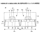
図2は、本発明の第1の実施の形態に係る電界効果型トランジスタの断面図である。
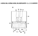
図6は、本発明の第2の実施の形態に係る電界効果型トランジスタの断面図である。図中、先に説明した部分に対応する部分には同一の参照符号を付し、説明を省略する。ここでは、説明の便宜のためpチャネルMISFETを例として説明する。なお、nチャネルMISFETは、ゲート電極とソース領域を構成する材料が、第1の実施の形態のように仕事関数の関係が設定されている以外はpチャネルMISFETと同様である。
図7は、本発明の第3の実施の形態に係る電界効果型トランジスタの断面図である。
(付記1) 半導体材料からなるチャネル領域と、チャネル領域を覆うゲート絶縁膜と、ゲート絶縁膜を覆うゲート電極と、
前記チャネル領域の両側にそれぞれ直接接触し、金属材料からなるソース領域およびドレイン領域と、を備えるnチャネルの電界効果型トランジスタであって、
前記ゲート電極の金属材料の仕事関数Wgとソース領域の金属材料の仕事関数Wsとの関係がWg<Wsであることを特徴とする電界効果型トランジスタ。
(付記2) 半導体材料からなるチャネル領域と、チャネル領域を覆うゲート絶縁膜と、ゲート絶縁膜を覆うゲート電極と、
前記チャネル領域の両側にそれぞれ直接接触し、金属材料からなるソース領域およびドレイン領域と、を備えるpチャネルの電界効果型トランジスタであって、
前記ゲート電極の金属材料の仕事関数Wgとソース領域の金属材料の仕事関数Wsとの関係がWg>Wsであることを特徴とする電界効果型トランジスタ。
(付記3) 付記1に記載のnチャネルの電界効果型トランジスタと付記2に記載のpチャネルの電界効果型トランジスタからなる相補型の電界効果型トランジスタ。
(付記4) 前記金属材料は、単金属、合金、および導電性の金属間化合物からなる群のうち、いずれか1種であることを特徴とする付記1〜3のうち、いずれか一項記載の電界効果型トランジスタ。
(付記5) 前記金属間化合物は、金属のシリサイド、ジャーマナイド、およびジャーマノシリサイドからなる群のうちいずれか1種であることを特徴とする付記4記載の電界効果型トランジスタ。
(付記6) 半導体材料からなるチャネル領域と、チャネル領域を覆うゲート絶縁膜と、ゲート絶縁膜を覆うゲート電極と、
前記チャネル領域の両側にそれぞれ直接接触し、金属材料からなるソース領域およびドレイン領域と、を備えるnチャネルの電界効果型トランジスタであって、
前記ゲート電極はSbがドープされたNiSiからなり、前記ソース領域はNiSiからなることを特徴とする電界効果型トランジスタ。
(付記7) 半導体材料からなるチャネル領域と、チャネル領域を覆うゲート絶縁膜と、ゲート絶縁膜を覆うゲート電極と、
前記チャネル領域の両側にそれぞれ直接接触し、金属材料からなるソース領域およびドレイン領域と、を備えるpチャネルの電界効果型トランジスタであって、
前記ゲート電極はAlがドープされたNiSiからなり、前記ソース領域はNiSiからなることを特徴とする電界効果型トランジスタ。
(付記8) 前記ゲート電極は、前記金属材料がゲート絶縁膜に直接接触することを特徴とする付記1〜7のうち、いずれか一項記載の電界効果型トランジスタ。
(付記9) 前記ゲート絶縁膜は、シリコン窒化膜、シリコン酸窒化膜、Al2O3膜、Ta2O5膜、HfO2膜、およびZrO2膜からなる群のうち少なくとも1つからなることを特徴とする付記1〜8のうち、いずれか一項記載の電界効果型トランジスタ。
(付記10) 前記チャネル領域は、Si層またはSi基板に形成されてなることを特徴とする付記1〜9のうち、いずれか一項記載の電界効果型トランジスタ。
(付記11) 前記チャネル領域は、真性Si層あるいは真性Si基板に形成されてなることを特徴とする付記10記載の電界効果型トランジスタ。
(付記12) 前記チャネル領域は、圧縮歪みが誘起されたSi1-xGex層からなることを特徴とする付記1〜9のうち、いずれか一項記載の電界効果型トランジスタ(ただしxはGeの組成比であり、0より大きくかつ1以下である。)。
(付記13) 前記チャネル領域は、Si基板表面にエピタキシャル成長したSi1-xGex層からなることを特徴とする付記12記載の電界効果型トランジスタ。
(付記14) 前記Si1-xGex層上にさらに緩和したSi層を有することを特徴とする付記12または13記載の電界効果型トランジスタ。
(付記15) 前記チャネル領域は、絶縁性基板上のSi層またはSi1-xGex層に設けられてなり、
前記ソース領域およびドレイン領域は、絶縁性基板上に前記金属材料から形成されてなることを特徴とする付記1〜9のうち、いずれか一項記載の電界効果型トランジスタ(ただしxはGeの組成比であり、0より大きくかつ1以下である。)。
(付記16) 前記ソース領域およびドレイン領域は、前記Si層またはSi1-xGex層に設けられたシリサイド膜、ジャーマノシリサイド膜、またはジャーマナイド膜からなることを特徴とする付記15記載の電界効果型トランジスタ。
(付記17) nチャネルの電界効果型トランジスタの製造方法であって、
Si基板表面にゲート絶縁膜および多結晶Siからなるゲート電極を形成する工程と、
前記ゲート電極の両側のSi基板の一部をシリサイドに変換してソース領域およびドレイン領域を形成すると共に、前記ゲート電極をシリサイド膜に変換する工程と、を備え、
前記ゲート電極を形成する工程は、ゲート電極に不純物を注入する処理を含み、ゲート電極の金属材料の仕事関数Wgとソース領域の金属材料の仕事関数WsとがWg<Wsなる関係を有するように該不純物を選択することを特徴とする電界効果型トランジスタの製造方法。
(付記18) pチャネルの電界効果型トランジスタの製造方法であって、
Si基板表面にゲート絶縁膜および多結晶Siからなるゲート電極を形成する工程と、
前記ゲート電極の両側のSi基板の一部をシリサイドに変換してソース領域およびドレイン領域を形成すると共に、前記ゲート電極をシリサイド膜に変換する工程と、を備え、
前記ゲート電極を形成する工程は、ゲート電極に不純物を注入する処理を含み、ゲート電極の金属材料の仕事関数Wgとソース領域の金属材料の仕事関数WsとがWg>Wsなる関係を有するように該不純物を選択することを特徴とする電界効果型トランジスタの製造方法。
(付記19) 前記ゲート電極の形成は、ポリシリコン膜を形成し、次いで該ポリシリコン膜に不純物を導入し、
前記不純物によりシリサイド膜に変換後の仕事関数Wgを制御することを特徴とする付記17または18記載の電界効果型トランジスタの製造方法。
11、61、76n、76p ソース領域
12、62、78n、78p ドレイン領域
13 ゲート電極
14 チャネル領域
15 ゲート絶縁膜
21 Si基板
22 素子分離領域
23n 第1領域
23p 第2領域
24n、74n nチャネルMISFET
24p、74p pチャネルMISFET
25n p型ウェル領域
25p n型ウェル領域
26、61 ソース領域
28、62 ドレイン領域
29 チャネル領域
30 ゲート絶縁膜
31n、31p ゲート電極
32、52 ゲート積層体
33 側壁絶縁膜
35 層間絶縁膜
38、39、40 レジスト膜
51 バリア膜
63 SiGe層
64 Siキャップ層
Claims (10)
- 半導体材料からなるチャネル領域と、チャネル領域を覆うゲート絶縁膜と、ゲート絶縁膜を覆うゲート電極と、
前記チャネル領域の両側にそれぞれ直接接触し、金属材料からなるソース領域およびドレイン領域と、を備えるnチャネルの電界効果型トランジスタであって、
前記ゲート電極の金属材料の仕事関数Wgとソース領域の金属材料の仕事関数Wsとの関係がWg<Wsであることを特徴とする電界効果型トランジスタ。 - 半導体材料からなるチャネル領域と、チャネル領域を覆うゲート絶縁膜と、ゲート絶縁膜を覆うゲート電極と、
前記チャネル領域の両側にそれぞれ直接接触し、金属材料からなるソース領域およびドレイン領域と、を備えるpチャネルの電界効果型トランジスタであって、
前記ゲート電極の金属材料の仕事関数Wgとソース領域の金属材料の仕事関数Wsとの関係がWg>Wsであることを特徴とする電界効果型トランジスタ。 - 前記金属材料は、金属、合金、および導電性の金属間化合物からなる群のうち、いずれか1種であることを特徴とする請求項1または2記載の電界効果型トランジスタ。
- 半導体材料からなるチャネル領域と、チャネル領域を覆うゲート絶縁膜と、ゲート絶縁膜を覆うゲート電極と、
前記チャネル領域の両側にそれぞれ直接接触し、金属材料からなるソース領域およびドレイン領域と、を備えるnチャネルの電界効果型トランジスタであって、
前記ゲート電極はSbがドープされたNiSiからなり、前記ソース領域はNiSiからなることを特徴とする電界効果型トランジスタ。 - 半導体材料からなるチャネル領域と、チャネル領域を覆うゲート絶縁膜と、ゲート絶縁膜を覆うゲート電極と、
前記チャネル領域の両側にそれぞれ直接接触し、金属材料からなるソース領域およびドレイン領域と、を備えるpチャネルの電界効果型トランジスタであって、
前記ゲート電極はAlがドープされたNiSiからなり、前記ソース領域はNiSiからなることを特徴とする電界効果型トランジスタ。 - 前記ゲート電極は、前記金属材料がゲート絶縁膜に直接接触することを特徴とする請求項1〜5のうち、いずれか一項記載の電界効果型トランジスタ。
- 前記チャネル領域は、圧縮歪みが誘起されたSi1-xGex層からなることを特徴とする請求項1〜6のうち、いずれか一項記載の電界効果型トランジスタ(ただしxはGeの組成比であり、0より大きくかつ1以下である。)。
- 前記チャネル領域は、絶縁性基板上のSi層またはSi1-xGex層に設けられてなり、
前記ソース領域およびドレイン領域は、絶縁性基板上に前記金属材料から形成されてなることを特徴とする請求項1〜7のうち、いずれか一項記載の電界効果型トランジスタ(ただしxはGeの組成比であり、0より大きくかつ1以下である。)。 - nチャネルの電界効果型トランジスタの製造方法であって、
Si基板表面にゲート絶縁膜および多結晶Siからなるゲート電極を形成する工程と、
前記ゲート電極の両側のSi基板の一部をシリサイドに変換してソース領域およびドレイン領域を形成すると共に、前記ゲート電極をシリサイド膜に変換する工程と、を備え、
前記ゲート電極を形成する工程は、ゲート電極に不純物を注入する処理を含み、ゲート電極の金属材料の仕事関数Wgとソース領域の金属材料の仕事関数WsとがWg<Wsなる関係を有するように該不純物を選択することを特徴とする電界効果型トランジスタの製造方法。 - pチャネルの電界効果型トランジスタの製造方法であって、
Si基板表面にゲート絶縁膜および多結晶Siからなるゲート電極を形成する工程と、
前記ゲート電極の両側のSi基板の一部をシリサイドに変換してソース領域およびドレイン領域を形成すると共に、前記ゲート電極をシリサイド膜に変換する工程と、を備え、
前記ゲート電極を形成する工程は、ゲート電極に不純物を注入する処理を含み、ゲート電極の金属材料の仕事関数Wgとソース領域の金属材料の仕事関数WsとがWg>Wsなる関係を有するように該不純物を選択することを特徴とする電界効果型トランジスタの製造方法。
Priority Applications (2)
| Application Number | Priority Date | Filing Date | Title |
|---|---|---|---|
| JP2004282235A JP4116990B2 (ja) | 2004-09-28 | 2004-09-28 | 電界効果型トランジスタおよびその製造方法 |
| US11/058,251 US7564061B2 (en) | 2004-09-28 | 2005-02-16 | Field effect transistor and production method thereof |
Applications Claiming Priority (1)
| Application Number | Priority Date | Filing Date | Title |
|---|---|---|---|
| JP2004282235A JP4116990B2 (ja) | 2004-09-28 | 2004-09-28 | 電界効果型トランジスタおよびその製造方法 |
Publications (2)
| Publication Number | Publication Date |
|---|---|
| JP2006100403A true JP2006100403A (ja) | 2006-04-13 |
| JP4116990B2 JP4116990B2 (ja) | 2008-07-09 |
Family
ID=36179858
Family Applications (1)
| Application Number | Title | Priority Date | Filing Date |
|---|---|---|---|
| JP2004282235A Expired - Fee Related JP4116990B2 (ja) | 2004-09-28 | 2004-09-28 | 電界効果型トランジスタおよびその製造方法 |
Country Status (2)
| Country | Link |
|---|---|
| US (1) | US7564061B2 (ja) |
| JP (1) | JP4116990B2 (ja) |
Cited By (12)
| Publication number | Priority date | Publication date | Assignee | Title |
|---|---|---|---|---|
| WO2009090974A1 (ja) * | 2008-01-16 | 2009-07-23 | Nec Corporation | 半導体装置及びその製造方法 |
| JP2009260004A (ja) * | 2008-04-16 | 2009-11-05 | Renesas Technology Corp | 半導体装置の製造方法 |
| JP2010505274A (ja) * | 2006-09-29 | 2010-02-18 | 東京エレクトロン株式会社 | 歪みゲルマニウム含有層を有するデバイスのためのuv支援による誘電層形成 |
| JP2011519152A (ja) * | 2008-04-11 | 2011-06-30 | サントル ナシオナル ドゥ ラ ルシェルシェサイアンティフィク(セエヌエールエス) | 相補型p、及びnMOSFETトランジスタの製造方法、このトランジスタを包含する電子デバイス、及び少なくとも1つのこのデバイスを包含するプロセッサ |
| JP2012507865A (ja) * | 2008-11-05 | 2012-03-29 | マイクロン テクノロジー, インク. | 複数のトランジスタゲートの形成方法、および少なくとも二つの異なる仕事関数を有する複数のトランジスタゲートの形成方法 |
| WO2012169212A1 (ja) * | 2011-06-10 | 2012-12-13 | 住友化学株式会社 | 半導体デバイス、半導体基板、半導体基板の製造方法および半導体デバイスの製造方法 |
| WO2012169210A1 (ja) * | 2011-06-10 | 2012-12-13 | 住友化学株式会社 | 半導体デバイス、半導体基板、半導体基板の製造方法および半導体デバイスの製造方法 |
| WO2012169209A1 (ja) * | 2011-06-10 | 2012-12-13 | 住友化学株式会社 | 半導体デバイス、半導体基板、半導体基板の製造方法および半導体デバイスの製造方法 |
| US8692320B2 (en) | 2006-05-11 | 2014-04-08 | Micron Technology, Inc. | Recessed memory cell access devices and gate electrodes |
| US8710583B2 (en) | 2006-05-11 | 2014-04-29 | Micron Technology, Inc. | Dual work function recessed access device and methods of forming |
| CN111739927A (zh) * | 2019-03-25 | 2020-10-02 | 三星电子株式会社 | 半导体器件和制造半导体器件的方法 |
| JP2023017736A (ja) * | 2021-07-23 | 2023-02-07 | 發明與合作實驗室有限公司 | 制御可能なソース/ドレイン構造を有するトランジスタ |
Families Citing this family (11)
| Publication number | Priority date | Publication date | Assignee | Title |
|---|---|---|---|---|
| US20070001231A1 (en) * | 2005-06-29 | 2007-01-04 | Amberwave Systems Corporation | Material systems for dielectrics and metal electrodes |
| US7432139B2 (en) * | 2005-06-29 | 2008-10-07 | Amberwave Systems Corp. | Methods for forming dielectrics and metal electrodes |
| US8860174B2 (en) | 2006-05-11 | 2014-10-14 | Micron Technology, Inc. | Recessed antifuse structures and methods of making the same |
| JP2008117842A (ja) * | 2006-11-01 | 2008-05-22 | Toshiba Corp | 半導体装置、およびその製造方法 |
| ITMI20070353A1 (it) * | 2007-02-23 | 2008-08-24 | Univ Padova | Transistore ad effetto di campo con giunzione metallo-semiconduttore. |
| JP5117740B2 (ja) * | 2007-03-01 | 2013-01-16 | ルネサスエレクトロニクス株式会社 | 半導体装置の製造方法 |
| US8753936B2 (en) * | 2008-08-12 | 2014-06-17 | International Business Machines Corporation | Changing effective work function using ion implantation during dual work function metal gate integration |
| JP2010093029A (ja) * | 2008-10-07 | 2010-04-22 | Toshiba Corp | 半導体装置およびその製造方法 |
| US8329568B1 (en) * | 2010-05-03 | 2012-12-11 | Xilinx, Inc. | Semiconductor device and method for making the same |
| TWI550828B (zh) * | 2011-06-10 | 2016-09-21 | 住友化學股份有限公司 | 半導體裝置、半導體基板、半導體基板之製造方法及半導體裝置之製造方法 |
| WO2016048377A1 (en) * | 2014-09-26 | 2016-03-31 | Intel Corporation | Metal oxide metal field effect transistors (momfets) |
Family Cites Families (10)
| Publication number | Priority date | Publication date | Assignee | Title |
|---|---|---|---|---|
| JPS5515263A (en) | 1978-07-19 | 1980-02-02 | Chiyou Lsi Gijutsu Kenkyu Kumiai | Mos type semiconductor device |
| JP3513018B2 (ja) | 1998-06-30 | 2004-03-31 | 株式会社東芝 | 半導体装置及びその製造方法 |
| JP2002011613A (ja) | 2000-06-23 | 2002-01-15 | Rex Industries Co Ltd | パイプ切断用カッター刃 |
| JP3833903B2 (ja) | 2000-07-11 | 2006-10-18 | 株式会社東芝 | 半導体装置の製造方法 |
| JP2002118175A (ja) | 2000-10-05 | 2002-04-19 | Toshiba Corp | 半導体装置及びその製造方法 |
| US6891234B1 (en) * | 2004-01-07 | 2005-05-10 | Acorn Technologies, Inc. | Transistor with workfunction-induced charge layer |
| JP2005085949A (ja) * | 2003-09-08 | 2005-03-31 | Semiconductor Leading Edge Technologies Inc | 半導体装置およびその製造方法 |
| US6906360B2 (en) * | 2003-09-10 | 2005-06-14 | International Business Machines Corporation | Structure and method of making strained channel CMOS transistors having lattice-mismatched epitaxial extension and source and drain regions |
| US7183182B2 (en) * | 2003-09-24 | 2007-02-27 | International Business Machines Corporation | Method and apparatus for fabricating CMOS field effect transistors |
| US7365432B2 (en) * | 2004-08-23 | 2008-04-29 | Taiwan Semiconductor Manufacturing Company, Ltd. | Memory cell structure |
-
2004
- 2004-09-28 JP JP2004282235A patent/JP4116990B2/ja not_active Expired - Fee Related
-
2005
- 2005-02-16 US US11/058,251 patent/US7564061B2/en not_active Expired - Fee Related
Cited By (16)
| Publication number | Priority date | Publication date | Assignee | Title |
|---|---|---|---|---|
| US8692320B2 (en) | 2006-05-11 | 2014-04-08 | Micron Technology, Inc. | Recessed memory cell access devices and gate electrodes |
| US9543433B2 (en) | 2006-05-11 | 2017-01-10 | Micron Technology, Inc. | Dual work function recessed access device and methods of forming |
| US9502516B2 (en) | 2006-05-11 | 2016-11-22 | Micron Technology, Inc. | Recessed access devices and gate electrodes |
| US8710583B2 (en) | 2006-05-11 | 2014-04-29 | Micron Technology, Inc. | Dual work function recessed access device and methods of forming |
| JP2010505274A (ja) * | 2006-09-29 | 2010-02-18 | 東京エレクトロン株式会社 | 歪みゲルマニウム含有層を有するデバイスのためのuv支援による誘電層形成 |
| WO2009090974A1 (ja) * | 2008-01-16 | 2009-07-23 | Nec Corporation | 半導体装置及びその製造方法 |
| JP2011519152A (ja) * | 2008-04-11 | 2011-06-30 | サントル ナシオナル ドゥ ラ ルシェルシェサイアンティフィク(セエヌエールエス) | 相補型p、及びnMOSFETトランジスタの製造方法、このトランジスタを包含する電子デバイス、及び少なくとも1つのこのデバイスを包含するプロセッサ |
| JP2009260004A (ja) * | 2008-04-16 | 2009-11-05 | Renesas Technology Corp | 半導体装置の製造方法 |
| JP2012507865A (ja) * | 2008-11-05 | 2012-03-29 | マイクロン テクノロジー, インク. | 複数のトランジスタゲートの形成方法、および少なくとも二つの異なる仕事関数を有する複数のトランジスタゲートの形成方法 |
| US8524561B2 (en) | 2008-11-05 | 2013-09-03 | Micron Technology, Inc. | Methods of forming a plurality of transistor gates, and methods of forming a plurality of transistor gates having at least two different work functions |
| WO2012169209A1 (ja) * | 2011-06-10 | 2012-12-13 | 住友化学株式会社 | 半導体デバイス、半導体基板、半導体基板の製造方法および半導体デバイスの製造方法 |
| WO2012169210A1 (ja) * | 2011-06-10 | 2012-12-13 | 住友化学株式会社 | 半導体デバイス、半導体基板、半導体基板の製造方法および半導体デバイスの製造方法 |
| WO2012169212A1 (ja) * | 2011-06-10 | 2012-12-13 | 住友化学株式会社 | 半導体デバイス、半導体基板、半導体基板の製造方法および半導体デバイスの製造方法 |
| CN111739927A (zh) * | 2019-03-25 | 2020-10-02 | 三星电子株式会社 | 半导体器件和制造半导体器件的方法 |
| JP2023017736A (ja) * | 2021-07-23 | 2023-02-07 | 發明與合作實驗室有限公司 | 制御可能なソース/ドレイン構造を有するトランジスタ |
| JP7530656B2 (ja) | 2021-07-23 | 2024-08-08 | 發明與合作實驗室有限公司 | 制御可能なソース/ドレイン構造を有するトランジスタ |
Also Published As
| Publication number | Publication date |
|---|---|
| US7564061B2 (en) | 2009-07-21 |
| JP4116990B2 (ja) | 2008-07-09 |
| US20060081947A1 (en) | 2006-04-20 |
Similar Documents
| Publication | Publication Date | Title |
|---|---|---|
| JP4116990B2 (ja) | 電界効果型トランジスタおよびその製造方法 | |
| CN108735673B (zh) | 半导体装置 | |
| CN103155123B (zh) | 具有SiGe沟道的pFET结分布的结构和方法 | |
| US7119402B2 (en) | Field effect transistor and manufacturing method thereof | |
| JP5178152B2 (ja) | 相補型半導体装置及びその製造方法 | |
| US9245807B2 (en) | Integrated circuit with a thin body field effect transistor and capacitor | |
| US7452764B2 (en) | Gate-induced strain for MOS performance improvement | |
| US20090085123A1 (en) | Semiconductor device and method for fabricating the same | |
| US7825433B2 (en) | MIS-type semiconductor device | |
| JP2009032955A (ja) | 半導体装置、およびその製造方法 | |
| CN103262246A (zh) | 用于具有高介电常数/金属栅极MOSFET的Vt调整和短沟道控制的结构和方法 | |
| US8557693B2 (en) | Contact resistivity reduction in transistor devices by deep level impurity formation | |
| TW200939398A (en) | Semiconductor structure and method of manufacturing thereof | |
| KR20130028941A (ko) | 매립된 소스/드레인 실리사이드를 위한 델타 단분자층 도펀트 에피택시 | |
| US11257934B2 (en) | Fin field-effect transistors with enhanced strain and reduced parasitic capacitance | |
| JP2006100600A (ja) | 半導体装置およびその製造方法 | |
| US8242485B2 (en) | Source/drain technology for the carbon nano-tube/graphene CMOS with a single self-aligned metal silicide process | |
| US7316959B2 (en) | Semiconductor device and method for fabricating the same | |
| US8247279B2 (en) | Method of fabricating semiconductor device using epitaxial growth inhibiting layers | |
| JP2004200335A (ja) | 絶縁ゲート型電界効果トランジスタを含む半導体装置及びその製造方法 | |
| JP6840199B2 (ja) | 半導体装置 | |
| US20060199343A1 (en) | Method of forming MOS transistor having fully silicided metal gate electrode | |
| JP2006278818A (ja) | 半導体装置 | |
| JPH10209296A (ja) | 半導体装置及びその製造方法 |
Legal Events
| Date | Code | Title | Description |
|---|---|---|---|
| A621 | Written request for application examination |
Free format text: JAPANESE INTERMEDIATE CODE: A621 Effective date: 20060126 |
|
| A977 | Report on retrieval |
Free format text: JAPANESE INTERMEDIATE CODE: A971007 Effective date: 20071022 |
|
| A131 | Notification of reasons for refusal |
Free format text: JAPANESE INTERMEDIATE CODE: A131 Effective date: 20071030 |
|
| A521 | Request for written amendment filed |
Free format text: JAPANESE INTERMEDIATE CODE: A523 Effective date: 20071227 |
|
| TRDD | Decision of grant or rejection written | ||
| A01 | Written decision to grant a patent or to grant a registration (utility model) |
Free format text: JAPANESE INTERMEDIATE CODE: A01 Effective date: 20080408 |
|
| A61 | First payment of annual fees (during grant procedure) |
Free format text: JAPANESE INTERMEDIATE CODE: A61 Effective date: 20080418 |
|
| FPAY | Renewal fee payment (event date is renewal date of database) |
Free format text: PAYMENT UNTIL: 20110425 Year of fee payment: 3 |
|
| R150 | Certificate of patent or registration of utility model |
Free format text: JAPANESE INTERMEDIATE CODE: R150 |
|
| FPAY | Renewal fee payment (event date is renewal date of database) |
Free format text: PAYMENT UNTIL: 20110425 Year of fee payment: 3 |
|
| FPAY | Renewal fee payment (event date is renewal date of database) |
Free format text: PAYMENT UNTIL: 20110425 Year of fee payment: 3 |
|
| FPAY | Renewal fee payment (event date is renewal date of database) |
Free format text: PAYMENT UNTIL: 20120425 Year of fee payment: 4 |
|
| FPAY | Renewal fee payment (event date is renewal date of database) |
Free format text: PAYMENT UNTIL: 20130425 Year of fee payment: 5 |
|
| LAPS | Cancellation because of no payment of annual fees |