JP7536246B2 - Detection device - Google Patents
Detection device Download PDFInfo
- Publication number
- JP7536246B2 JP7536246B2 JP2022578436A JP2022578436A JP7536246B2 JP 7536246 B2 JP7536246 B2 JP 7536246B2 JP 2022578436 A JP2022578436 A JP 2022578436A JP 2022578436 A JP2022578436 A JP 2022578436A JP 7536246 B2 JP7536246 B2 JP 7536246B2
- Authority
- JP
- Japan
- Prior art keywords
- photodiode
- signal
- detection
- circuit
- voltage
- Prior art date
- Legal status (The legal status is an assumption and is not a legal conclusion. Google has not performed a legal analysis and makes no representation as to the accuracy of the status listed.)
- Active
Links
Images






Classifications
-
- H—ELECTRICITY
- H10—SEMICONDUCTOR DEVICES; ELECTRIC SOLID-STATE DEVICES NOT OTHERWISE PROVIDED FOR
- H10F—INORGANIC SEMICONDUCTOR DEVICES SENSITIVE TO INFRARED RADIATION, LIGHT, ELECTROMAGNETIC RADIATION OF SHORTER WAVELENGTH OR CORPUSCULAR RADIATION
- H10F39/00—Integrated devices, or assemblies of multiple devices, comprising at least one element covered by group H10F30/00, e.g. radiation detectors comprising photodiode arrays
- H10F39/10—Integrated devices
- H10F39/107—Integrated devices having multiple elements covered by H10F30/00 in a repetitive configuration, e.g. radiation detectors comprising photodiode arrays
-
- A—HUMAN NECESSITIES
- A61—MEDICAL OR VETERINARY SCIENCE; HYGIENE
- A61B—DIAGNOSIS; SURGERY; IDENTIFICATION
- A61B5/00—Measuring for diagnostic purposes; Identification of persons
- A61B5/117—Identification of persons
- A61B5/1171—Identification of persons based on the shapes or appearances of their bodies or parts thereof
-
- A—HUMAN NECESSITIES
- A61—MEDICAL OR VETERINARY SCIENCE; HYGIENE
- A61B—DIAGNOSIS; SURGERY; IDENTIFICATION
- A61B5/00—Measuring for diagnostic purposes; Identification of persons
- A61B5/117—Identification of persons
- A61B5/1171—Identification of persons based on the shapes or appearances of their bodies or parts thereof
- A61B5/1172—Identification of persons based on the shapes or appearances of their bodies or parts thereof using fingerprinting
-
- A—HUMAN NECESSITIES
- A61—MEDICAL OR VETERINARY SCIENCE; HYGIENE
- A61B—DIAGNOSIS; SURGERY; IDENTIFICATION
- A61B5/00—Measuring for diagnostic purposes; Identification of persons
- A61B5/145—Measuring characteristics of blood in vivo, e.g. gas concentration or pH-value ; Measuring characteristics of body fluids or tissues, e.g. interstitial fluid or cerebral tissue
- A61B5/1455—Measuring characteristics of blood in vivo, e.g. gas concentration or pH-value ; Measuring characteristics of body fluids or tissues, e.g. interstitial fluid or cerebral tissue using optical sensors, e.g. spectral photometrical oximeters
-
- H—ELECTRICITY
- H04—ELECTRIC COMMUNICATION TECHNIQUE
- H04N—PICTORIAL COMMUNICATION, e.g. TELEVISION
- H04N25/00—Circuitry of solid-state image sensors [SSIS]; Control thereof
- H04N25/70—SSIS architectures; Circuits associated therewith
-
- H—ELECTRICITY
- H10—SEMICONDUCTOR DEVICES; ELECTRIC SOLID-STATE DEVICES NOT OTHERWISE PROVIDED FOR
- H10F—INORGANIC SEMICONDUCTOR DEVICES SENSITIVE TO INFRARED RADIATION, LIGHT, ELECTROMAGNETIC RADIATION OF SHORTER WAVELENGTH OR CORPUSCULAR RADIATION
- H10F30/00—Individual radiation-sensitive semiconductor devices in which radiation controls the flow of current through the devices, e.g. photodetectors
- H10F30/20—Individual radiation-sensitive semiconductor devices in which radiation controls the flow of current through the devices, e.g. photodetectors the devices having potential barriers, e.g. phototransistors
- H10F30/21—Individual radiation-sensitive semiconductor devices in which radiation controls the flow of current through the devices, e.g. photodetectors the devices having potential barriers, e.g. phototransistors the devices being sensitive to infrared, visible or ultraviolet radiation
- H10F30/288—Individual radiation-sensitive semiconductor devices in which radiation controls the flow of current through the devices, e.g. photodetectors the devices having potential barriers, e.g. phototransistors the devices being sensitive to infrared, visible or ultraviolet radiation the devices being sensitive to multiple wavelengths, e.g. multi-spectrum radiation detection devices
-
- H—ELECTRICITY
- H10—SEMICONDUCTOR DEVICES; ELECTRIC SOLID-STATE DEVICES NOT OTHERWISE PROVIDED FOR
- H10F—INORGANIC SEMICONDUCTOR DEVICES SENSITIVE TO INFRARED RADIATION, LIGHT, ELECTROMAGNETIC RADIATION OF SHORTER WAVELENGTH OR CORPUSCULAR RADIATION
- H10F39/00—Integrated devices, or assemblies of multiple devices, comprising at least one element covered by group H10F30/00, e.g. radiation detectors comprising photodiode arrays
- H10F39/10—Integrated devices
- H10F39/12—Image sensors
-
- H—ELECTRICITY
- H10—SEMICONDUCTOR DEVICES; ELECTRIC SOLID-STATE DEVICES NOT OTHERWISE PROVIDED FOR
- H10F—INORGANIC SEMICONDUCTOR DEVICES SENSITIVE TO INFRARED RADIATION, LIGHT, ELECTROMAGNETIC RADIATION OF SHORTER WAVELENGTH OR CORPUSCULAR RADIATION
- H10F39/00—Integrated devices, or assemblies of multiple devices, comprising at least one element covered by group H10F30/00, e.g. radiation detectors comprising photodiode arrays
- H10F39/10—Integrated devices
- H10F39/12—Image sensors
- H10F39/18—Complementary metal-oxide-semiconductor [CMOS] image sensors; Photodiode array image sensors
- H10F39/182—Colour image sensors
- H10F39/1825—Multicolour image sensors having stacked structure, e.g. NPN, NPNPN or multiple quantum well [MQW] structures
-
- H—ELECTRICITY
- H10—SEMICONDUCTOR DEVICES; ELECTRIC SOLID-STATE DEVICES NOT OTHERWISE PROVIDED FOR
- H10K—ORGANIC ELECTRIC SOLID-STATE DEVICES
- H10K39/00—Integrated devices, or assemblies of multiple devices, comprising at least one organic radiation-sensitive element covered by group H10K30/00
- H10K39/10—Organic photovoltaic [PV] modules; Arrays of single organic PV cells
Landscapes
- Health & Medical Sciences (AREA)
- Life Sciences & Earth Sciences (AREA)
- Physics & Mathematics (AREA)
- Engineering & Computer Science (AREA)
- Surgery (AREA)
- Animal Behavior & Ethology (AREA)
- Biomedical Technology (AREA)
- Heart & Thoracic Surgery (AREA)
- Medical Informatics (AREA)
- Molecular Biology (AREA)
- Biophysics (AREA)
- Pathology (AREA)
- General Health & Medical Sciences (AREA)
- Public Health (AREA)
- Veterinary Medicine (AREA)
- Spectroscopy & Molecular Physics (AREA)
- Optics & Photonics (AREA)
- Multimedia (AREA)
- Signal Processing (AREA)
- Solid State Image Pick-Up Elements (AREA)
Description
本発明は、検出装置に関する。The present invention relates to a detection device.
指紋パターンや血管パターンを検出可能な光センサが知られている(例えば、特許文献1)。このような光センサでは、活性層として有機半導体材料が用いられたフレキシブルなシートセンサが知られている。Optical sensors capable of detecting fingerprint patterns and vein patterns are known (for example, see Patent Document 1). Among such optical sensors, flexible sheet sensors using an organic semiconductor material as an active layer are known.
光センサでは、検出の際に逆バイアス電圧が供給され、感度特性が経時的に変化する可能性がある。In an optical sensor, a reverse bias voltage is supplied during detection, and the sensitivity characteristics may change over time.
本発明は、感度特性の変化を抑制することが可能な検出装置を提供することを目的とする。An object of the present invention is to provide a detection device capable of suppressing changes in sensitivity characteristics.
本発明の一態様の検出装置は、基板の上に配列された複数の光センサを有する検出装置であって、複数の前記光センサは、それぞれ、第1フォトダイオードと、前記第1フォトダイオードと直列に、かつ、逆方向に接続される第2フォトダイオードと、を有する。A detection device of one embodiment of the present invention is a detection device having a plurality of optical sensors arranged on a substrate, each of the plurality of optical sensors having a first photodiode and a second photodiode connected in series and in the reverse direction to the first photodiode.
本発明を実施するための形態(実施形態)につき、図面を参照しつつ詳細に説明する。以下の実施形態に記載した内容により本発明が限定されるものではない。また、以下に記載した構成要素には、当業者が容易に想定できるもの、実質的に同一のものが含まれる。さらに、以下に記載した構成要素は適宜組み合わせることが可能である。なお、開示はあくまで一例にすぎず、当業者において、発明の主旨を保っての適宜変更について容易に想到し得るものについては、当然に本発明の範囲に含有されるものである。また、図面は説明をより明確にするため、実際の態様に比べ、各部の幅、厚さ、形状等について模式的に表される場合があるが、あくまで一例であって、本発明の解釈を限定するものではない。また、本明細書と各図において、既出の図に関して前述したものと同様の要素には、同一の符号を付して、詳細な説明を適宜省略することがある。The form (embodiment) for carrying out the present invention will be described in detail with reference to the drawings. The present invention is not limited by the contents described in the following embodiment. In addition, the components described below include those that a person skilled in the art can easily imagine and those that are substantially the same. Furthermore, the components described below can be appropriately combined. Note that the disclosure is merely an example, and those that a person skilled in the art can easily imagine appropriate modifications while maintaining the gist of the invention are naturally included in the scope of the present invention. In addition, in order to make the explanation clearer, the drawings may be schematic in terms of the width, thickness, shape, etc. of each part compared to the actual embodiment, but they are merely examples and do not limit the interpretation of the present invention. In addition, in this specification and each figure, elements similar to those described above with respect to the previously mentioned figures may be given the same reference numerals, and detailed explanations may be omitted as appropriate.
本明細書及び請求の範囲において、ある構造体の上に他の構造体を配置する態様を表現するにあたり、単に「上に」と表記する場合、特に断りの無い限りは、ある構造体に接するように、直上に他の構造体を配置する場合と、ある構造体の上方に、さらに別の構造体を介して他の構造体を配置する場合との両方を含むものとする。In this specification and claims, when expressing an aspect of arranging another structure on top of a certain structure, the term "on top" is used, unless otherwise specified, to include both a case in which another structure is arranged directly on top of a certain structure so as to be in contact with the certain structure, and a case in which another structure is arranged above a certain structure via yet another structure.
(第1実施形態)
図1は、第1実施形態に係る検出装置を示す平面図である。図1に示すように、検出装置1は、センサ基材21と、センサ部10と、ゲート線駆動回路15と、信号線選択回路16と、検出回路48と、制御回路122と、電源回路123と、第1光源基材51と、第2光源基材52と、第1光源61と、第2光源62と、を有する。第1光源基材51には、複数の第1光源61が設けられる。第2光源基材52には複数の第2光源62が設けられる。First Embodiment
Fig. 1 is a plan view showing a detection device according to the first embodiment. As shown in Fig. 1, the
センサ基材21には、フレキシブルプリント基板71を介して制御基板121が電気的に接続される。フレキシブルプリント基板71には、検出回路48が設けられている。制御基板121には、制御回路122及び電源回路123が設けられている。制御回路122は、例えばFPGA(Field Programmable Gate Array)である。制御回路122は、センサ部10、ゲート線駆動回路15及び信号線選択回路16に制御信号を供給して、センサ部10の検出動作を制御する。また、制御回路122は、第1光源61及び第2光源62に制御信号を供給して、第1光源61及び第2光源62の点灯又は非点灯を制御する。電源回路123は、駆動信号VDDSNS(図4参照)等の電圧信号をセンサ部10、ゲート線駆動回路15及び信号線選択回路16に供給する。また、電源回路123は、電源電圧を第1光源61及び第2光源62に供給する。The
センサ基材21は、検出領域AAと、周辺領域GAとを有する。検出領域AAは、センサ部10が有する複数の光センサPD(図4参照)が設けられた領域である。周辺領域GAは、検出領域AAの外周と、センサ基材21の端部との間の領域であり、光センサPDが設けられない領域である。The
ゲート線駆動回路15及び信号線選択回路16は、周辺領域GAに設けられる。具体的には、ゲート線駆動回路15は、周辺領域GAのうち第2方向Dyに沿って延在する領域に設けられる。信号線選択回路16は、周辺領域GAのうち第1方向Dxに沿って延在する領域に設けられ、センサ部10と検出回路48との間に設けられる。The gate
なお、第1方向Dxは、センサ基材21と平行な面内の一方向である。第2方向Dyは、センサ基材21と平行な面内の一方向であり、第1方向Dxと直交する方向である。なお、第2方向Dyは、第1方向Dxと直交しないで交差してもよい。The first direction Dx is a direction in a plane parallel to the
複数の第1光源61は、第1光源基材51に設けられ、第2方向Dyに沿って配列される。複数の第2光源62は、第2光源基材52に設けられ、第2方向Dyに沿って配列される。第1光源基材51及び第2光源基材52は、それぞれ、制御基板121に設けられた端子部124、125を介して、制御回路122及び電源回路123と電気的に接続される。The
複数の第1光源61及び複数の第2光源62は、例えば、無機LED(Light Emitting Diode)や、有機EL(OLED:Organic Light Emitting Diode)等が用いられ
る。複数の第1光源61及び複数の第2光源62は、それぞれ異なる波長の第1光及び第2光を出射する。 The
第1光源61から出射された第1光は、主に指Fg等の被検出体の表面で反射されセンサ部10に入射する。これにより、センサ部10は、指Fg等の表面の凹凸の形状を検出することで指紋を検出することができる。第2光源62から出射された第2光は、主に指Fg等の内部で反射し又は指Fg等を透過してセンサ部10に入射する。これにより、センサ部10は、指Fg等の内部の生体に関する情報を検出できる。生体に関する情報とは、例えば、指Fgや掌の脈波、脈拍、血管像等である。すなわち、検出装置1は、指紋を検出する指紋検出装置や、静脈などの血管パターンを検出する静脈検出装置として構成されてもよい。The first light emitted from the
第1光は、500nm以上600nm以下、例えば550nm程度の波長を有し、第2光は、780nm以上950nm以下、例えば850nm程度の波長を有していてもよい。この場合、第1光は、青色又は緑色の可視光であり、第2光は、赤外光である。センサ部10は、第1光源61から出射された第1光に基づいて、指紋を検出することができる。第2光源62から出射された第2光は、指Fg等の被検出体の内部で反射し又は指Fg等を透過・吸収されてセンサ部10に入射する。これにより、センサ部10は、指Fg等の内部の生体に関する情報として脈波や血管像(血管パターン)を検出できる。The first light may have a wavelength of 500 nm or more and 600 nm or less, for example, about 550 nm, and the second light may have a wavelength of 780 nm or more and 950 nm or less, for example, about 850 nm. In this case, the first light is blue or green visible light, and the second light is infrared light. The
又は、第1光は、600nm以上700nm以下、例えば660nm程度の波長を有し、第2光は、780nm以上900nm以下、例えば850nm程度の波長を有していてもよい。この場合、第1光源61から出射された第1光及び第2光源62から出射された第2光に基づいて、センサ部10は、生体に関する情報として、脈波、脈拍や血管像に加えて、血中酸素飽和度を検出することができる。このように、検出装置1は、第1光源61及び複数の第2光源62を有しているので、第1光に基づいた検出と、第2光に基づいた検出とを行うことで、種々の生体に関する情報を検出することができる。Alternatively, the first light may have a wavelength of 600 nm or more and 700 nm or less, for example, about 660 nm, and the second light may have a wavelength of 780 nm or more and 900 nm or less, for example, about 850 nm. In this case, based on the first light emitted from the
なお、図1に示す第1光源61及び第2光源62の配置は、あくまで一例であり適宜変更することができる。検出装置1は、光源として複数種類の光源(第1光源61と第2光源62)が設けられている。ただし、これに限定されず、光源は1種類であってもよい。例えば、第1光源基材51及び第2光源基材52のそれぞれに、複数の第1光源61及び複数の第2光源62が配置されていてもよい。また、第1光源61及び第2光源62が設けられる光源基材は1つ又は3つ以上であってもよい。あるいは、光源は、少なくとも1つ以上配置されていればよい。ただし、これに限定されず、検出装置1(第1フォトダイオードPDaと第2フォトダイオードPDb(図4参照))が検出感度を有する異なる波長領域にわたる光を出射する1種類の光源であってもよい。The arrangement of the
図2は、第1実施形態に係る検出装置の構成例を示すブロック図である。図2に示すように、検出装置1は、さらに検出制御部11と検出部40と、有する。検出制御部11の機能の一部又は全部は、制御回路122に含まれる。また、検出部40のうち、検出回路48以外の機能の一部又は全部は、制御回路122に含まれる。Fig. 2 is a block diagram showing an example of the configuration of the detection device according to the first embodiment. As shown in Fig. 2, the
センサ部10は、複数の光センサPDを有する。センサ部10が有する光センサPDはフォトダイオードであり、照射される光に応じた電気信号を、検出信号Vdetとして信号線選択回路16に出力する。また、センサ部10は、ゲート線駆動回路15から供給されるゲート駆動信号Vgclにしたがって検出を行う。The
検出制御部11は、ゲート線駆動回路15、信号線選択回路16及び検出部40にそれぞれ制御信号を供給し、これらの動作を制御する回路である。検出制御部11は、スタート信号STV、クロック信号CK、リセット信号RST1等の各種制御信号をゲート線駆動回路15に供給する。また、検出制御部11は、選択信号ASW等の各種制御信号を信号線選択回路16に供給する。また、検出制御部11は、各種制御信号を第1光源61及び第2光源62に供給して、それぞれの点灯及び非点灯を制御する。The detection control unit 11 is a circuit that supplies control signals to the gate
ゲート線駆動回路15は、各種制御信号に基づいて複数のゲート線GCL(図3参照)を駆動する回路である。ゲート線駆動回路15は、複数のゲート線GCLを順次又は同時に選択し、選択されたゲート線GCLにゲート駆動信号Vgclを供給する。これにより、ゲート線駆動回路15は、ゲート線GCLに電気的に接続された複数の光センサPDを選択する。The gate
信号線選択回路16は、複数の信号線SGL(図3参照)を順次又は同時に選択するスイッチ回路である。信号線選択回路16は、例えばマルチプレクサである。信号線選択回路16は、検出制御部11から供給される選択信号ASWに基づいて、選択された信号線SGLと検出回路48とを電気的に接続する。これにより、信号線選択回路16は、光センサPDの検出信号Vdetを検出部40に出力する。The signal
検出部40は、検出回路48と、信号処理部44と、座標抽出部45と、記憶部46と、検出タイミング制御部47と、画像処理部49と、出力処理部50とを備える。検出タイミング制御部47は、検出制御部11から供給される制御信号に基づいて、検出回路48と、信号処理部44と、座標抽出部45と、画像処理部49と、が同期して動作するように制御する。The
検出回路48は、例えばアナログフロントエンド回路(AFE、Analog Front End)である。検出回路48は、少なくとも検出信号増幅部42及びA/D変換部43の機能を有する信号処理回路である。検出信号増幅部42は、検出信号Vdetを増幅する。A/D変換部43は、検出信号増幅部42から出力されるアナログ信号をデジタル信号に変換する。The
信号処理部44は、検出回路48の出力信号に基づいて、センサ部10に入力された所定の物理量を検出する論理回路である。信号処理部44は、指Fgが検出面に接触又は近接した場合に、検出回路48からの信号に基づいて指Fgや掌の表面の凹凸を検出できる。また、信号処理部44は、検出回路48からの信号に基づいて生体に関する情報を検出できる。生体に関する情報は、例えば、指Fgや掌の血管像、脈波、脈拍、血中酸素濃度等である。The
また、信号処理部44は、複数の光センサPDにより同時に検出された検出信号Vdet(生体に関する情報)を取得し、これらを平均化する処理を実行してもよい。この場合、検出部40は、ノイズや、指Fg等の被検出体とセンサ部10との相対的な位置ずれに起因する測定誤差を抑制して、安定した検出が可能となる。The
記憶部46は、信号処理部44で演算された信号を一時的に保存する。記憶部46は、例えばRAM(Random Access Memory)、レジスタ回路等であってもよい。The
座標抽出部45は、信号処理部44において指の接触又は近接が検出されたときに、指等の表面の凹凸の検出座標を求める論理回路である。また、座標抽出部45は、指Fgや掌の血管の検出座標を求める論理回路である。画像処理部49は、センサ部10の各光センサPDから出力される検出信号Vdetを組み合わせて、指Fg等の表面の凹凸の形状を示す二次元情報及び指Fgや掌の血管の形状を示す二次元情報を生成する。なお、座標抽出部45は、検出座標を算出せずにセンサ出力電圧Voとして検出信号Vdetを出力してもよい。また、座標抽出部45及び画像処理部49は、検出部40に含まれていない場合であってもよい。The coordinate
出力処理部50は、複数の光センサPDからの出力に基づいた処理を行う処理部として機能する。具体的には、実施形態の出力処理部50は、少なくとも、信号処理部44を経て取得された検出信号Vdetに基づいて、少なくとも脈波データを含むセンサ出力電圧Voを出力する。実施形態では、後述する各光センサPDの検出信号Vdetの出力電圧の変化(振幅)を示すデータを信号処理部44が出力し、どの出力がセンサ出力電圧Voに採用されるかを出力処理部50が決定するが、この両方を信号処理部44又は出力処理部50が行うようにしてもよい。なお、出力処理部50は、座標抽出部45が求めた検出座標、画像処理部49が生成した二次元情報等をセンサ出力電圧Voに含めるようにしてもよい。また、出力処理部50の機能は、他の構成(例えば、画像処理部49等)に統合されてもよい。The
次に、検出装置1の回路構成例について説明する。図3は、検出装置を示す回路図である。図3に示すように、センサ部10は、マトリクス状に配列された複数の部分検出領域PAAを有する。複数の部分検出領域PAAには、それぞれ光センサPDが設けられている。すなわち、複数の光センサPDは、センサ基材21上にマトリクス状に配列される。Next, an example of the circuit configuration of the
ゲート線GCLは、第1方向Dxに延在し、第1方向Dxに配列された複数の部分検出領域PAAと電気的に接続される。また、複数のゲート線GCL(1)、GCL(2)、…、GCL(8)は、第2方向Dyに配列され、それぞれゲート線駆動回路15に電気的に接続される。なお、以下の説明において、複数のゲート線GCL(1)、GCL(2)、…、GCL(8)を区別して説明する必要がない場合には、単にゲート線GCLと表す。また、図3では説明を分かりやすくするために、8本のゲート線GCLを示しているが、あくまで一例であり、ゲート線GCLは、M本(Mは8以上、例えばM=256)配列されていてもよい。The gate line GCL extends in the first direction Dx and is electrically connected to a plurality of partial detection areas PAA arranged in the first direction Dx. The plurality of gate lines GCL(1), GCL(2), ..., GCL(8) are arranged in the second direction Dy and are each electrically connected to the gate
信号線SGLは、第2方向Dyに延在し、第2方向Dyに配列された複数の部分検出領域PAAの光センサPDに電気的に接続される。また、複数の信号線SGL(1)、SGL(2)、…、SGL(12)は、第1方向Dxに配列されて、それぞれ信号線選択回路16及びリセット回路17に電気的に接続される。なお、以下の説明において、複数の信号線SGL(1)、SGL(2)、…、SGL(12)を区別して説明する必要がない場合には、単に信号線SGLと表す。The signal line SGL extends in the second direction Dy and is electrically connected to the optical sensors PD of the partial detection areas PAA arranged in the second direction Dy. The signal lines SGL(1), SGL(2), ..., SGL(12) are arranged in the first direction Dx and are each electrically connected to the signal
また、説明を分かりやすくするために、12本の信号線SGLを示しているが、あくまで一例であり、信号線SGLは、N本(Nは12以上、例えばN=252)配列されていてもよい。また、図3では、信号線選択回路16とリセット回路17との間にセンサ部10が設けられている。これに限定されず、信号線選択回路16とリセット回路17とは、信号線SGLの同じ方向の端部にそれぞれ電気的に接続されていてもよい。また、1つのセンサの実質的な面積は例えば実質50×50um2とされ、検出領域AAの解像度は例えば実質508ppiとされ、検出領域AAに配置されるセンサ数は例えば252セル×256セルとされ、検出領域AAの面積は例えば12.6×12.8mm2とされる。 In addition, to make the explanation easier to understand, 12 signal lines SGL are shown, but this is merely an example, and N signal lines SGL (N is 12 or more, for example, N=252) may be arranged. In addition, in FIG. 3, the
ゲート線駆動回路15は、スタート信号STV、クロック信号CK、リセット信号RST1等の各種制御信号を、制御回路122(図1参照)から受け取る。ゲート線駆動回路15は、各種制御信号に基づいて、複数のゲート線GCL(1)、GCL(2)、…、GCL(8)を時分割的に順次選択する。ゲート線駆動回路15は、選択されたゲート線GCLにゲート駆動信号Vgclを供給する。これにより、ゲート線GCLに電気的に接続された複数の第1スイッチング素子Trにゲート駆動信号Vgclが供給され、第1方向Dxに配列された複数の部分検出領域PAAが、検出対象として選択される。The gate
なお、ゲート線駆動回路15は、指紋の検出及び異なる複数の生体に関する情報(脈波、脈拍、血管像、血中酸素濃度等)のそれぞれの検出モードごとに、異なる駆動を実行してもよい。例えば、ゲート線駆動回路15は、複数のゲート線GCLを束ねて駆動してもよい。The gate
信号線選択回路16は、複数の選択信号線Lselと、複数の出力信号線Loutと、第3スイッチング素子TrSと、を有する。複数の第3スイッチング素子TrSは、それぞれ複数の信号線SGLに対応して設けられている。6本の信号線SGL(1)、SGL(2)、…、SGL(6)は、共通の出力信号線Lout1に電気的に接続される。6本の信号線SGL(7)、SGL(8)、…、SGL(12)は、共通の出力信号線Lout2に電気的に接続される。出力信号線Lout1、Lout2は、それぞれ検出回路48に電気的に接続される。The signal
ここで、信号線SGL(1)、SGL(2)、…、SGL(6)を第1信号線ブロックとし、信号線SGL(7)、SGL(8)、…、SGL(12)を第2信号線ブロックとする。複数の選択信号線Lselは、1つの信号線ブロックに含まれる第3スイッチング素子TrSのゲートにそれぞれ電気的に接続される。また、1本の選択信号線Lselは、複数の信号線ブロックの第3スイッチング素子TrSのゲートに電気的に接続される。Here, the signal lines SGL(1), SGL(2), ..., SGL(6) are defined as a first signal line block, and the signal lines SGL(7), SGL(8), ..., SGL(12) are defined as a second signal line block. The multiple selection signal lines Lsel are each electrically connected to the gate of the third switching element TrS included in one signal line block. Furthermore, one selection signal line Lsel is electrically connected to the gate of the third switching element TrS of the multiple signal line blocks.
制御回路122(図1参照)は、選択信号ASWを順次選択信号線Lselに供給する。これにより、信号線選択回路16は、第3スイッチング素子TrSの動作により、1つの信号線ブロックにおいて信号線SGLを時分割的に順次選択する。また、信号線選択回路16は、複数の信号線ブロックでそれぞれ1本ずつ信号線SGLを選択する。このような構成により、検出装置1は、検出回路48を含むIC(Integrated Circuit)の数、
又はICの端子数を少なくすることができる。なお、信号線選択回路16は、複数の信号線SGLを束ねて検出回路48に電気的に接続してもよい。 The control circuit 122 (see FIG. 1) sequentially supplies the selection signal ASW to the selection signal line Lsel. As a result, the signal
Alternatively, the number of terminals of the IC can be reduced. The signal
図3に示すように、リセット回路17は、基準信号線Lvr、リセット信号線Lrst及び第4スイッチング素子TrRを有する。第4スイッチング素子TrRは、複数の信号線SGLに対応して設けられている。基準信号線Lvrは、複数の第4スイッチング素子TrRのソース又はドレインの一方に電気的に接続される。リセット信号線Lrstは、複数の第4スイッチング素子TrRのゲートに電気的に接続される。3, the
制御回路122は、リセット信号RST2をリセット信号線Lrstに供給する。これにより、複数の第4スイッチング素子TrRがオンになり、複数の信号線SGLは基準信号線Lvrと電気的に接続される。電源回路123は、基準電位COMを基準信号線Lvrに供給する。これにより、複数の部分検出領域PAAに含まれる容量素子Ca(図4参照)に基準電位COMが供給される。The
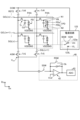
図4は、複数の部分検出領域を示す回路図である。なお、図4では、検出回路48の回路構成も併せて示している。図4に示すように、部分検出領域PAAは、光センサPDと、容量素子Caと、第1スイッチング素子Trとを含む。容量素子Caは、光センサPDに形成される容量(センサ容量)であり、等価的に光センサPDと並列に電気的に接続される。Fig. 4 is a circuit diagram showing a plurality of partial detection areas. Fig. 4 also shows the circuit configuration of a
図4では、複数のゲート線GCLのうち、第2方向Dyに並ぶ2つのゲート線GCL(m)、GCL(m+1)を示す。また、複数の信号線SGLのうち、第1方向Dxに並ぶ2つの信号線SGL(n)、SGL(n+1)を示す。部分検出領域PAAは、ゲート線GCLと信号線SGLとで囲まれた領域である。4 shows two gate lines GCL(m) and GCL(m+1) arranged in the second direction Dy among the multiple gate lines GCL. Also, two signal lines SGL(n) and SGL(n+1) arranged in the first direction Dx among the multiple signal lines SGL. The partial detection area PAA is an area surrounded by the gate lines GCL and the signal lines SGL.
第1スイッチング素子Trは、光センサPDに対応して設けられる。第1スイッチング素子Trは、薄膜トランジスタにより構成されるものであり、この例では、nチャネルのMOS(Metal Oxide Semiconductor)型のTFT(Thin Film Transistor)で構成
されている。 The first switching element Tr is provided corresponding to the optical sensor PD. The first switching element Tr is configured of a thin film transistor, and in this example, is configured of an n-channel MOS (Metal Oxide Semiconductor) type TFT (Thin Film Transistor).
第1方向Dxに並ぶ複数の部分検出領域PAAに属する第1スイッチング素子Trのゲートは、ゲート線GCLに電気的に接続される。第2方向Dyに並ぶ複数の部分検出領域PAAに属する第1スイッチング素子Trのソースは、信号線SGLに電気的に接続される。第1スイッチング素子Trのドレインは、光センサPDの一端側の第1端子N1及び容量素子Caに電気的に接続される。The gates of the first switching elements Tr belonging to the partial detection areas PAA aligned in the first direction Dx are electrically connected to the gate line GCL. The sources of the first switching elements Tr belonging to the partial detection areas PAA aligned in the second direction Dy are electrically connected to the signal line SGL. The drains of the first switching elements Tr are electrically connected to the first terminal N1 on one end side of the photosensor PD and the capacitance element Ca.
光センサPDは、第1フォトダイオードPDaと、第2フォトダイオードPDbと、を有する。第1フォトダイオードPDa及び第2フォトダイオードPDbは、光センサPDの一端側の第1端子N1と他端側の第2端子N2との間で、直列に、かつ逆方向に接続される。なお、「逆方向に接続」とは、第1フォトダイオードPDaと、第2フォトダイオードPDbとで整流特性が逆方向になる接続構成を示す。より具体的には、第1フォトダイオードPDaのカソードが第1端子N1に電気的に接続され、第1フォトダイオードPDaのアノードと第2フォトダイオードPDbのアノードとが電気的に接続され、第2フォトダイオードPDbのカソードが第2端子N2に電気的に接続される。The optical sensor PD has a first photodiode PDa and a second photodiode PDb. The first photodiode PDa and the second photodiode PDb are connected in series and in reverse between a first terminal N1 on one end side of the optical sensor PD and a second terminal N2 on the other end side. Note that "connected in reverse" refers to a connection configuration in which the rectification characteristics of the first photodiode PDa and the second photodiode PDb are in reverse directions. More specifically, the cathode of the first photodiode PDa is electrically connected to the first terminal N1, the anode of the first photodiode PDa and the anode of the second photodiode PDb are electrically connected, and the cathode of the second photodiode PDb is electrically connected to the second terminal N2.
光センサPDの第2端子N2(第2フォトダイオードPDbのカソード)には、駆動信号供給回路123aから駆動信号VDDSNSが供給される。駆動信号供給回路123aは、電源回路123に設けられる。ただし、これに限定されず、駆動信号供給回路123aは、制御回路122に設けられていてもよいし、センサ基材21上に設けられていてもよい。また、信号線SGL及び第1端子N1(容量素子Ca及び光センサPD)には、電源回路123から、信号線SGL及び第1端子N1(容量素子Ca及び光センサPD)の初期電位となる基準電位COMが供給される。駆動信号VDDSNSと基準電位COMとで、光センサPDにバイアス電圧VBが供給される。バイアス電圧VBは、VB=COM-VDDSNSで表される。A drive signal VDDSNS is supplied from a drive
光センサPDに駆動信号VDDSNSを供給する駆動信号供給回路123aは、第1電圧信号供給部123Hと、第2電圧信号供給部123Lと、スイッチBSWとを備える。第1電圧信号供給部123Hは、基準電位COMよりも高レベル電圧の第1電圧信号VHを供給する回路である。第2電圧信号供給部123Lは、基準電位COMよりも低レベル電圧の第2電圧信号VLを供給する回路である。スイッチBSWは、第1電圧信号供給部123H及び第2電圧信号供給部123Lと、光センサPDの第2端子N2と、の接続状態を切り替えるスイッチ素子である。スイッチBSWの動作により、駆動信号供給回路123aは、第1電圧信号VHと、第2電圧信号VLとを時分割で光センサPDの第2端子N2に供給する。The drive
駆動信号供給回路123aから、光センサPDの第2端子N2に第1電圧信号VH(VH>COM)が供給された場合、第1フォトダイオードPDaが順バイアス駆動され、第2フォトダイオードPDbが逆バイアス駆動される。この場合、第2フォトダイオードPDbが検出を行い、第1フォトダイオードPDaには順方向の電流が流れる。例えば、基準電位COMは0.75Vとされ、第1電圧信号VHは2.75Vとされる。この場合、バイアス電圧VBは、VB=0.75-2.75=-2.0Vとなる。When the first voltage signal VH (VH>COM) is supplied from the drive
駆動信号供給回路123aから、光センサPDの第2端子N2に第2電圧信号VL(VL<COM)が供給された場合、第1フォトダイオードPDaが逆バイアス駆動され、第2フォトダイオードPDbが順バイアス駆動される。この場合、第1フォトダイオードPDaが検出を行い、第2フォトダイオードPDbには順方向の電流が流れる。例えば、基準電位COMは0.75Vとされ、第2電圧信号VLは-1.25Vとされる。この場合、バイアス電圧VBは、VB=0.75-(-1.25)=+2.0Vとなる。When the second voltage signal VL (VL<COM) is supplied from the drive
部分検出領域PAAに光が照射されると、光センサPD(第1フォトダイオードPDa又は第2フォトダイオードPDb)には光量に応じた電流が流れ、これにより容量素子Caに電荷が蓄積される。第1スイッチング素子Trがオンになると、容量素子Caに蓄積された電荷に応じて、信号線SGLに電流が流れる。信号線SGLは、信号線選択回路16の第3スイッチング素子TrSを介して検出回路48に電気的に接続される。これにより、検出装置1は、部分検出領域PAAごとに、又はブロック単位PAGごとに光センサPDに照射される光の光量に応じた信号を検出できる。When light is irradiated onto the partial detection area PAA, a current corresponding to the amount of light flows through the photosensor PD (the first photodiode PDa or the second photodiode PDb), causing charge to accumulate in the capacitance element Ca. When the first switching element Tr is turned on, a current flows through the signal line SGL according to the charge accumulated in the capacitance element Ca. The signal line SGL is electrically connected to the
検出回路48は、読み出し期間Pdet(図7参照)にスイッチSSWがオンになり、信号線SGLと電気的に接続される。検出回路48の検出信号増幅部42は、信号線SGLから供給された電流の変動を電圧の変動に変換して増幅する。検出信号増幅部42の非反転入力部(+)には、固定された電位を有する基準電位(Vref)が入力され、反転入力端子(-)には、信号線SGLが電気的に接続される。実施形態では、基準電位(Vref)電圧として基準電位COMと同じ信号が入力される。信号処理部44(図2参照)は、光が照射された場合の検出信号Vdetと、光が照射されていない場合の検出信号Vdetとの差分をセンサ出力電圧Voとして演算する。また、検出信号増幅部42は、容量素子Cb及びリセットスイッチRSWを有する。リセット期間Prst(図7参照)において、リセットスイッチRSWがオンになり、容量素子Cbの電荷がリセットされる。In the
ここで、光センサPD(OPD:Organic Photo Diode)が形成される有機半導体層
にバラツキが生じた場合、OPDの特性にバラツキが生じて検出精度が低下する可能性がある。以下、有機半導体層にバラツキが生じた場合の光センサPDのダイオード特性について、図5を参照して説明する。 Here, if there is variation in the organic semiconductor layer in which the optical sensor PD (OPD: Organic Photo Diode) is formed, there is a possibility that the characteristics of the OPD will vary and the detection accuracy will decrease. Hereinafter, the diode characteristics of the optical sensor PD when there is variation in the organic semiconductor layer will be described with reference to FIG.
図5は、光センサのダイオード特性の一例を示す図である。図5において、横軸は電流を示し、縦軸は電圧を示している。また、図5において、実線は正常時のダイオード特性を示し、破線はOPDの特性バラツキによる特性変化の一例を示している。Fig. 5 is a diagram showing an example of the diode characteristics of an optical sensor. In Fig. 5, the horizontal axis represents current and the vertical axis represents voltage. In Fig. 5, the solid line represents the diode characteristics under normal conditions, and the dashed line represents an example of characteristic changes due to characteristic variations of the OPD.
光センサPD(OPD:Organic Photo Diode)が形成される有機半導体層のバラツ
キにより、OPDの逆方向特性が破線で示したように変化する場合がある。これにより、後述する露光期間(実効露光期間)において光センサPDに流れる逆方向電流が部分検出領域PAAごとにバラツキが生じることとなり、検出精度が低下する。 Due to variations in the organic semiconductor layer in which the optical sensor PD (OPD: Organic Photo Diode) is formed, the reverse characteristic of the OPD may change as shown by the dashed line. This causes variations in the reverse current flowing through the optical sensor PD during an exposure period (effective exposure period) described later for each partial detection area PAA, thereby reducing the detection accuracy.
本実施形態では、所定のタイミングで光センサPDに順方向バイアス電流を流すことで、OPDの特性を初期状態(図5に示す実線)に戻す。本開示では、このOPDの特性を初期状態に戻す動作を、「リフレッシュ動作」と称する。In this embodiment, a forward bias current is passed through the photosensor PD at a predetermined timing to return the characteristics of the OPD to the initial state (solid line shown in FIG. 5 ). In this disclosure, the operation of returning the characteristics of the OPD to the initial state is referred to as a “refresh operation.”
次に、光センサPDの構成について説明する。図6は、センサ部の概略断面構成を示す断面図である。図6に示すように、センサ部10は、センサ基材21と、TFT層22と、絶縁層23と、光センサPDと、中間層24と、封止層25と、保護層29と、を備える。センサ基材21は、絶縁性の基材であり、例えば、ガラスや樹脂材料が用いられる。センサ基材21は、平板状に限定されず、曲面を有していてもよい。この場合、センサ基材21は、フィルム状の樹脂であってもよい。センサ基材21は、第1面S1と、第1面の反対側の第2面S2とを有する。第1面S1に、TFT層22、絶縁層23、光センサPD、中間層24、封止層25、保護層29の順に積層される。本実施形態では、光L1が第2面S2側から光センサPDに照射される構成について説明する。ただし、これに限定されず、光L1が第1面S1側から光センサPDに照射される構成であってもよい。Next, the configuration of the optical sensor PD will be described. FIG. 6 is a cross-sectional view showing a schematic cross-sectional configuration of the sensor unit. As shown in FIG. 6, the
TFT層22は、上述したゲート線駆動回路15や信号線選択回路16等の回路が設けられる。また、TFT層22には、第1スイッチング素子Tr等のTFT(Thin Film Transistor)や、ゲート線GCL、信号線SGL等の各種配線が設けられる。センサ基材21及びTFT層22は、所定の検出領域ごとにセンサを駆動する駆動回路基板であり、バックプレーン又はアレイ基板とも呼ばれる。The
絶縁層23は、有機絶縁層であり、TFT層22の上に設けられる。絶縁層23は、TFT層22に形成される第1スイッチング素子Trや、各種導電層で形成される凹凸を平坦化する平坦化層である。The insulating
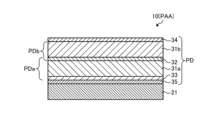
光センサPDは、絶縁層23の上に設けられる。光センサPDは、絶縁層23の上に第1フォトダイオードPDa、第2フォトダイオードPDbの順に積層される。より具体的には、光センサPDは、センサ基材21の第1面S1に垂直な方向で、下部電極35(第1電極)、電子輸送層33、第1活性層31a、正孔輸送層32、第2活性層31b、上部電極34(第2電極)の順に積層される。The optical sensor PD is provided on the insulating
下部電極35は、絶縁層23の上に設けられ、コンタクトホール(図示しない)を介してTFT層22の第1スイッチング素子Trと電気的に接続される。下部電極35は、第1フォトダイオードPDaのカソード(第1端子N1)であり、検出信号Vdetを読み出すための電極である。下部電極35は、例えば、ITO(Indium Tin Oxide)等の透光性を有する導電材料で形成される。The
第1活性層31a及び第2活性層31bは、照射される光に応じて特性(例えば、電圧電流特性や抵抗値)が変化する。第1活性層31a及び第2活性層31bの材料として、有機材料が用いられる。具体的には、第1活性層31a及び第2活性層31bは、p型有機半導体と、n型有機半導体であるn型フラーレン誘導体(PCBM)とが混在するバルクヘテロ構造である。第1活性層31a及び第2活性層31bとして、例えば、低分子有機材料であるC60(フラーレン)、PCBM(フェニルC61酪酸メチルエステル:[6,6]-Phenyl C61 butyric acid methyl ester)、CuPc(銅フタロシアニン:Copper Phthalocyanine)、F16CuPc(フッ素化銅フタロシアニン)、rubren
e(ルブレン:5,6,11,12-tetraphenyltetracene)、PDI(Perylene(ペリレン)の誘導体)等を用いることができる。 The characteristics (for example, voltage-current characteristics and resistance value) of the first
Examples of the usable materials include rubrene (5,6,11,12-tetraphenyltetracene), PDI (perylene derivative), and the like.
第1活性層31a及び第2活性層31bは、これらの低分子有機材料を用いて蒸着型(Dry Process)で形成することができる。この場合、第1活性層31a及び第2活性層31bは、例えば、CuPcとF16CuPcとの積層膜、又はrubreneとC60との積層膜であってもよい。第1活性層31a及び第2活性層31bは、塗布型(Wet Process)で形成することもできる。この場合、第1活性層31a及び第2活性層31bは、上述した低分子有機材料と高分子有機材料とを組み合わせた材料が用いられる。高分子有機材料として、例えばP3HT(poly(3-hexylthiophene))、F8BT(F8-alt-benzothiadiazole)等を用いることができる。第1活性層31a及び第2活性層31bは、P
3HTとPCBMとが混合した状態の膜、又はF8BTとPDIとが混合した状態の膜とすることができる。 The first
It can be a film of a mixture of 3HT and PCBM, or a film of a mixture of F8BT and PDI.
第1活性層31a及び第2活性層31bは、同じ材料で形成されてもよいし、異なる材料で形成されてもよい。例えば、第1活性層31aとして、P3HT:PCMB(P3HTとPCBMとが混合した状態の膜)を用いることができる。また、第2活性層31bとしてPMDPP3T(poly[[2,5-bis(2-hexyldecyl)-2,3,5,6-tetrahydro-3,6-dioxopyrrolo[3,4-c]pyrrole-1,4-diyl]-alt-[3′,3′'-dimethyl-2,2′:5′,2′'-terthiophene]-5,5′'-diyl]):PCBM([6,6]-Phenyl C61 butyric acid methyl ester)(P
MDPP3TとPCBMとが混合した状態の膜)を用いることができる。この場合、第1フォトダイオードPDaは、可視光(例えば400nm以上650nm以下の波長)に対し感度を有する。第2フォトダイオードPDbは、近赤外光(例えば780nm以上950nm以下の波長)に対し感度を有する。 The first
A film in which MDPP3T and PCBM are mixed can be used. In this case, the first photodiode PDa has sensitivity to visible light (for example, a wavelength of 400 nm or more and 650 nm or less). The second photodiode PDb has sensitivity to near-infrared light (for example, a wavelength of 780 nm or more and 950 nm or less).
上部電極34は、第2フォトダイオードPDbのカソード(第2端子N2)であり、駆動信号VDDSNSを光センサPDに供給するための電極である。上部電極34と、下部電極35とは、第1活性層31a及び第2活性層31bを挟んで対向する。上部電極34は、例えば、アルミニウム(Al)が用いられる。あるいは、上部電極34は、銀(Ag)等の金属材料、あるいは、これらの金属材料の少なくとも1以上を含む合金材料であってもよい。The
電子輸送層33及び正孔輸送層32は、第1活性層31a及び第2活性層31bで発生した正孔及び電子が上部電極34又は下部電極35に到達しやすくするために設けられる。電子輸送層33は、センサ基材21の第1面S1に垂直な方向で、下部電極35と第1活性層31aとの間に設けられる。電子輸送層33は、下部電極35の上に直接、接し、第1活性層31aは、電子輸送層33の上に直接、接する。電子輸送層33の材料は、エトキシ化ポリエチレンイミン(PEIE)又は酸化亜鉛(ZnO)が用いられる。The
正孔輸送層32は、センサ基材21の第1面S1に垂直な方向で、第1活性層31aと第2活性層31bとの間に設けられる。正孔輸送層32は、第1活性層31aの上に直接、接し、第2活性層31bは、正孔輸送層32の上に直接、接する。正孔輸送層32は、ポリチオフェン系導電性ポリマー(PEDOT(Poly(3,4-ethylenedioxythiophene)):PSS(poly(styrene sulfonate)))が用いられる。本実施形態では、正孔輸送層32は、第1フォトダイオードPDa及び第2フォトダイオードPDbに共用される。The
封止層25は、光センサPDを覆って設けられる。より具体的には、封止層25は、中間層24を介して上部電極34の上に設けられる。封止層25の材料は、酸化アルミニウム(Al2O3)である。これにより、検出装置1は、封止層25としてパリレンを用いた場合に比べて、光センサPDを良好に封止することができる。また、中間層24の材料は、ITOが用いられ、中間層24により、上部電極34と封止層25との間の密着性を向上させることができる。 The
保護層29は、封止層25を覆って設けられる。保護層29は、例えば樹脂フィルムが用いられる。保護層29は、光センサPDを保護するために設けられる。なお、保護層29の材料は、樹脂フィルムに限定されず、他の材料が用いられていてもよい。The
本実施形態では、光L1が第2面S2側から光センサPDに照射される構成について説明したが、光L1が第1面S1側から光センサPDに照射される構成であってもよい。この場合、上部電極34として、ITO等の透光性を有する導電材料が用いられ、下部電極35として、アルミニウム又は銀等の金属材料が用いられる。In the present embodiment, the light L1 is irradiated onto the optical sensor PD from the second surface S2 side, but the light L1 may be irradiated onto the optical sensor PD from the first surface S1 side. In this case, the
次に、検出装置1の動作例について説明する。図7は、検出装置の動作例を表すタイミング波形図である。なお、図7では、駆動信号VDDSNSとして主に第2電圧信号VLが供給された場合、すなわち、光センサPDの第1フォトダイオードPDaが検出する場合の動作を示す。ただし、図7の説明は、駆動信号VDDSNSとして第1電圧信号VHが供給された場合、すなわち、光センサPDの第2フォトダイオードPDbでの検出にも適用できる。Next, an operation example of the
図7に示すように、検出装置1は、リセット期間Prst、露光期間Pex及び読み出し期間Pdetを有する。電源回路123(駆動信号供給回路123a)は、リセット期間Prst、露光期間Pex及び読み出し期間Pdetに亘って、駆動信号VDDSNSを光センサPDのアノードに供給する。駆動信号VDDSNSは光センサPDの第1端子N1-第2端子N2間にバイアス電圧VBを印加する信号である。例えば、光センサPDの第1端子N1には実質0.75Vの基準電位COMがされているが、第2端子N2に実質-1.25Vの駆動信号VDDSNSを印加することにより、第1端子N1-第2端子N2間は実質2.0Vのバイアス電圧VBが供給される。制御回路122は、リセット信号RST2を”H”とした後にゲート線駆動回路15にスタート信号STVおよびクロック信号CKを供給し、リセット期間Prstが開始する。リセット期間Prstにおいて、制御回路122は、基準電位COMをリセット回路17に供給し、リセット信号RST2によってリセット電圧を供給するための第4スイッチング素子TrRをオンさせる。これにより各信号線SGLにはリセット電圧として基準電位COMが供給される。As shown in FIG. 7, the
リセット期間Prstにおいて、ゲート線駆動回路15は、スタート信号STV、クロック信号CK及びリセット信号RST1に基づいて、順次ゲート線GCLを選択する。ゲート線駆動回路15は、ゲート駆動信号Vgcl{Vgcl(1)~Vgcl(M)}をゲート線GCLに順次供給する。ゲート駆動信号Vgclは、高レベル電圧である電源電圧VDDと低レベル電圧である電源電圧VSSとを有するパルス状の波形を有する。図7では、M本(例えばM=256)のゲート線GCLが設けられており、各ゲート線GCLに、ゲート駆動信号Vgcl(1)、…、Vgcl(M)が順次供給され、複数の第1スイッチング素子Trは各行毎に順次導通され、リセット電圧が供給される。リセット電圧として例えば、基準電位COMの電圧0.75Vが供給される。In the reset period Prst, the gate
これにより、リセット期間Prstでは、全ての部分検出領域PAAの容量素子Caは、順次信号線SGLと電気的に接続されて、基準電位COMが供給される。この結果、容量素子Caの容量がリセットされる。尚、部分的にゲート線、および信号線SGLを選択することにより部分検出領域PAAのうち一部の容量素子Caの容量をリセットすることも可能である。As a result, in the reset period Prst, the capacitance elements Ca in all the partial detection areas PAA are sequentially electrically connected to the signal lines SGL and supplied with the reference potential COM. As a result, the capacitance of the capacitance elements Ca is reset. It is also possible to reset the capacitance of some of the capacitance elements Ca in the partial detection area PAA by partially selecting the gate lines and signal lines SGL.
露光するタイミングの例として、ゲート線非選択時露光制御方法と常時露光制御方法がある。ゲート線非選択時露光制御方法においては、検出対象の光センサPDに電気的に接続された全てのゲート線GCLにゲート駆動信号{Vgcl(1)~(M)}が順次供給され、検出対象の全ての光センサPDにリセット電圧が供給される。その後、検出対象の光センサPDに電気的に接続された全てのゲート線GCLが低電圧(第1スイッチング素子Trがオフ)になると露光が開始され、露光期間Pexの間に露光が行われる。露光が終了すると前述のように検出対象の光センサPDに電気的に接続されたゲート線GCLにゲート駆動信号{Vgcl(1)~(M)}が順次供給され、読み出し期間Pdetに読み出しが行われる。常時露光制御方法においては、リセット期間Prst、読み出し期間Pdetにおいても露光を行う制御(常時露光制御)をすることも可能である。この場合は、リセット期間Prstにゲート駆動信号Vgcl(1)がゲート線GCLに供給された直後に、実効露光期間SPex(1)が開始する。ここで、実効露光期間SPex{(1)・・・(M)}とは光センサPDから容量素子Caへ充電される期間とされる。すなわち常時露光制御方法においては、第1スイッチング素子Trがオフになったときに実効露光期間SPexが開始されることになる。リセット期間Prstに容量素子Caにチャージされた電荷が、光照射によって光センサPDに逆方向電流(カソードからアノードへ)として流れ、容量素子Caの電位差は減少する。なお、各ゲート線GCLに対応する部分検出領域PAAでの、実際の実効露光期間SPex(1)、…、SPex(M)は、開始のタイミング及び終了のタイミングが異なっている。実効露光期間SPex(1)、…、SPex(M)は、それぞれ、リセット期間Prstでゲート駆動信号Vgclが高レベル電圧の電源電圧VDDから低レベル電圧の電源電圧VSSに変化したタイミングで開始される。また、実効露光期間SPex(1)、…、SPex(M)は、それぞれ、読み出し期間Pdetでゲート駆動信号Vgclが電源電圧VSSから電源電圧VDDに変化したタイミングで終了する。各実効露光期間SPex(1)、…、SPex(M)の露光時間の長さは等しい。Examples of the timing of exposure include a gate line non-selection exposure control method and a constant exposure control method. In the gate line non-selection exposure control method, gate drive signals {Vgcl(1) to (M)} are sequentially supplied to all gate lines GCL electrically connected to the photosensor PD to be detected, and a reset voltage is supplied to all photosensors PD to be detected. After that, when all gate lines GCL electrically connected to the photosensor PD to be detected are at a low voltage (the first switching element Tr is off), exposure is started, and exposure is performed during the exposure period Pex. When exposure is completed, as described above, gate drive signals {Vgcl(1) to (M)} are sequentially supplied to the gate lines GCL electrically connected to the photosensor PD to be detected, and reading is performed during the readout period Pdet. In the constant exposure control method, it is also possible to control exposure to be performed during the reset period Prst and the readout period Pdet (constant exposure control). In this case, the effective exposure period SPex(1) starts immediately after the gate drive signal Vgcl(1) is supplied to the gate line GCL during the reset period Prst. Here, the effective exposure period SPex{(1)...(M)} is the period during which the capacitance element Ca is charged from the photosensor PD. That is, in the constant exposure control method, the effective exposure period SPex starts when the first switching element Tr is turned off. The charge charged in the capacitance element Ca during the reset period Prst flows as a reverse current (from the cathode to the anode) to the photosensor PD by light irradiation, and the potential difference of the capacitance element Ca decreases. Note that the actual effective exposure periods SPex(1),..., SPex(M) in the partial detection areas PAA corresponding to each gate line GCL have different start and end timings. Each of the effective exposure periods SPex(1), ..., SPex(M) starts when the gate drive signal Vgcl changes from the high-level voltage of the power supply voltage VDD to the low-level voltage of the power supply voltage VSS during the reset period Prst. Each of the effective exposure periods SPex(1), ..., SPex(M) ends when the gate drive signal Vgcl changes from the power supply voltage VSS to the power supply voltage VDD during the readout period Pdet. The exposure time of each of the effective exposure periods SPex(1), ..., SPex(M) is equal.
ゲート線非選択時露光制御方法において、露光期間Pex{(1)・・・(M)}では、各部分検出領域PAAで、光センサPDに照射された光に応じて電流が流れる。この結果、各容量素子Caに電荷が蓄積される。In the gate line non-selection exposure control method, in the exposure period Pex {(1)...(M)}, a current flows in each partial detection area PAA according to the light irradiated to the photosensor PD. As a result, a charge is accumulated in each capacitance element Ca.
読み出し期間Pdetが開始する前のタイミングで、制御回路122は、リセット信号RST2を低レベル電圧にする。これにより、リセット回路17の動作が停止する。尚、リセット信号はリセット期間Prstのみ高レベル電圧としてもよい。読み出し期間Pdetでは、リセット期間Prstと同様に、ゲート線駆動回路15は、ゲート線GCLにゲート駆動信号Vgcl(1)、…、Vgcl(M)を順次供給する。Before the readout period Pdet starts, the
具体的には、ゲート線駆動回路15は、期間V(1)において、ゲート線GCL(1)に、高レベル電圧(電源電圧VDD)のゲート駆動信号Vgcl(1)を供給する。制御回路122は、ゲート駆動信号Vgcl(1)が高レベル電圧(電源電圧VDD)の期間に、選択信号ASW1、…、ASW6を、信号線選択回路16に順次供給する。これにより、ゲート駆動信号Vgcl(1)により選択された部分検出領域PAAの信号線SGLが順次、又は同時に検出回路48に電気的に接続される。この結果、検出信号Vdetが部分検出領域PAAごとに検出回路48に供給される。Specifically, the gate
同様に、ゲート線駆動回路15は、期間V(2)、…、V(M-1)、V(M)において、ゲート線GCL(2)、…、GCL(M-1)、GCL(M)に、それぞれ高レベル電圧のゲート駆動信号Vgcl(2)、…、Vgcl(M-1)、Vgcl(M)を供給する。すなわち、ゲート線駆動回路15は、期間V(1)、V(2)、…、V(M-1)、V(M)ごとに、ゲート線GCLにゲート駆動信号Vgclを供給する。各ゲート駆動信号Vgclが高レベル電圧となる期間ごとに、信号線選択回路16は選択信号ASWに基づいて、順次信号線SGLを選択する。信号線選択回路16は、信号線SGLごとに順次、1つの検出回路48に電気的に接続する。これにより、読み出し期間Pdetで、検出装置1は、全ての部分検出領域PAAの検出信号Vdetを検出回路48に出力することができる。Similarly, the gate
図8は、図7における読み出し期間の動作例を表すタイミング波形図である。以下、図8を参照して、図7における1つのゲート駆動信号Vgcl(j)の供給期間Readoutでの動作例について説明する。図7では、最初のゲート駆動信号Vgcl(1)に供給期間Readoutの符号を付しているが、他のゲート駆動信号Vgcl(2)、…、Vgcl(M)についても同様である。jは、1からMのいずれかの自然数である。Fig. 8 is a timing waveform diagram showing an example of operation during the readout period in Fig. 7. Below, an example of operation during the supply period Readout of one gate drive signal Vgcl(j) in Fig. 7 will be described with reference to Fig. 8. In Fig. 7, the first gate drive signal Vgcl(1) is given the symbol of the supply period Readout, but the same is true for the other gate drive signals Vgcl(2), ..., Vgcl(M). j is any natural number from 1 to M.
図8および図4に示すように、第3スイッチング素子TrSの出力電圧(Vout)は予め基準電位(Vref)電圧にリセットされている。基準電位(Vref)電圧はリセット電圧とされ、例えば0.75Vとされる。次にゲート駆動信号Vgcl(j)がハイレベルとなり当該行の第1スイッチング素子Trがオンし、各行の信号線SGLは当該部分検出領域PAAの容量(容量素子Ca)に蓄積された電荷に応じた電圧になる。ゲート駆動信号Vgcl(j)の立ち上がりから期間t1の経過後、選択信号ASW(k)がハイになる期間t2が生じる。選択信号ASW(k)がハイになって第3スイッチング素子TrSがオンすると、当該第3スイッチング素子TrSを介して検出回路48と電気的に接続されている部分検出領域PAAの容量(容量素子Ca)に充電された電荷により、第3スイッチング素子TrSの出力電圧(Vout)(図4参照)が当該部分検出領域PAAの容量(容量素子Ca)に蓄積された電荷に応じた電圧に変化する(期間t3)。図8の例では期間t3のようにこの電圧はリセット電圧から下がっている。その後、スイッチSSWがオン(SSW信号のハイレベルの期間t4)すると当該部分検出領域PAAの容量(容量素子Ca)に蓄積された電荷が検出回路48の検出信号増幅部42の容量(容量素子Cb)へ電荷が移動し、検出信号増幅部42の出力電圧は容量素子Cbに蓄積された電荷に応じた電圧となる。このとき検出信号増幅部42の反転入力部はオペアンプのイマジナリショート電位となるため、基準電位(Vref)に戻っている。検出信号増幅部42の出力電圧はA/D変換部43で読み出す。図8の例では、各列の信号線SGLに対応する選択信号ASW(k)、ASW(k+1)、…の波形がハイになって第3スイッチング素子TrSを順次オンさせ、同様の動作を順次行うことで当該ゲート線GCLに電気的に接続された部分検出領域PAAの容量(容量素子Ca)に蓄積された電荷を順次読み出している。なお図8におけるASW(k)、ASW(k+1)…は、例えば、図8におけるASW1からASW6のいずれかである。 As shown in Fig. 8 and Fig. 4, the output voltage (V out ) of the third switching element TrS is reset to a reference potential (Vref) voltage in advance. The reference potential (Vref) voltage is a reset voltage, for example, 0.75 V. Next, the gate drive signal Vgcl(j) goes high, turning on the first switching element Tr of the row, and the signal line SGL of each row goes to a voltage according to the charge accumulated in the capacitance (capacitor element Ca) of the partial detection area PAA. After a period t1 has elapsed since the rising edge of the gate drive signal Vgcl(j), a period t2 occurs during which the selection signal ASW(k) goes high. When the selection signal ASW(k) becomes high and the third switching element TrS is turned on, the output voltage (V out ) (see FIG. 4 ) of the third switching element TrS changes to a voltage corresponding to the charge stored in the capacitance (capacitor Ca) of the partial detection area PAA, which is electrically connected to the
具体的には、スイッチSSWがオンになる期間t4が生じると、部分検出領域PAAの容量(容量素子Ca)から検出回路48の検出信号増幅部42の容量(容量素子Cb)へ電荷が移動する。このとき検出信号増幅部42の非反転入力(+)は、基準電位(Vref)電圧(例えば、0.75[V])にバイアスされている。このため、検出信号増幅部42の入力間のイマジナリショートにより第3スイッチング素子TrSの出力電圧(Vo
ut)も基準電位(Vref)電圧になる。また、容量素子Cbの電圧は、選択信号ASW(k)に応じて第3スイッチング素子TrSがオンした箇所の部分検出領域PAAの容量(容量素子Ca)に蓄積された電荷に応じた電圧となる。検出信号増幅部42の出力電圧は、イマジナリショートによって第3スイッチング素子TrSの出力電圧(Vout)が基準電位(Vref)電圧になった後に、容量素子Cbの容量に応じた電圧になり、この出力電圧をA/D変換部43で読み取る。なお、容量素子Cbの電圧とは、例えば、容量素子Cbを構成するコンデンサに設けられる2つの電極間の電圧である。 Specifically, when a period t4 occurs during which the switch SSW is turned on, charge moves from the capacitance (capacitor Ca) of the partial detection area PAA to the capacitance (capacitor Cb) of the
なお、期間t1は、例えば20[μs]である。期間t2は、例えば60[μs]である。期間t3は、例えば44.7[μs]である。期間t4は、例えば0.98[μs]である。The period t1 is, for example, 20 μs, the period t2 is, for example, 60 μs, the period t3 is, for example, 44.7 μs, and the period t4 is, for example, 0.98 μs.
なお、図7及び図8では、ゲート線駆動回路15がゲート線GCLを個別に選択する例を示したが、これに限定されない。ゲート線駆動回路15は、2以上の所定数のゲート線GCLを同時に選択し、所定数のゲート線GCLごとに順次ゲート駆動信号Vgclを供給してもよい。また、信号線選択回路16も、2以上の所定数の信号線SGLを同時に1つの検出回路48に電気的に接続してもよい。また更には、ゲート線駆動回路15は、複数のゲート線GCLを間引いて走査してもよい。7 and 8 show an example in which the gate
次に、バイアス電圧VBと、光センサPDの特性との関係について説明する。図9は、バイアス電圧と検出値との関係を模式的に示すグラフである。図9は、光センサPDの第1フォトダイオードPDa及び第2フォトダイオードPDbのそれぞれについて、バイアス電圧VBと検出値との関係を示している。図9に示すグラフの横軸は、光センサPDに供給されるバイアス電圧VBであり、縦軸は、光センサPDからの検出値を示す。検出値は、検出回路48から出力される電圧信号である。あるいは、検出値は、図4に示す第3スイッチング素子TrSの出力電圧(Vout)としてもよい。 Next, the relationship between the bias voltage VB and the characteristics of the optical sensor PD will be described. FIG. 9 is a graph that shows a schematic relationship between the bias voltage and the detection value. FIG. 9 shows the relationship between the bias voltage VB and the detection value for each of the first photodiode PDa and the second photodiode PDb of the optical sensor PD. The horizontal axis of the graph shown in FIG. 9 shows the bias voltage VB supplied to the optical sensor PD, and the vertical axis shows the detection value from the optical sensor PD. The detection value is a voltage signal output from the
また、図9では、第1フォトダイオードPDaは可視光(波長400nm以上650nm以下、例えば525nm)を検出し、第2フォトダイオードPDbは、近赤外光(波長780nm以上950nm以下、例えば850nm)を検出する場合について説明する。Also, in FIG. 9, a case will be described in which the first photodiode PDa detects visible light (
図9に示すように、バイアス電圧VBが負の極性の場合、第1フォトダイオードPDaが順バイアス駆動され、第2フォトダイオードPDbが逆バイアス駆動される。これにより、第2フォトダイオードPDbに流れる電流が検出される。したがって、バイアス電圧VBが負の極性の場合に、光センサPDは主に近赤外光に対して感度を有する。なお、第2フォトダイオードPDbは、近赤外光に加え、可視光にも感度を有する。このため、図9に示すように、バイアス電圧VBが負の極性において、光センサPDは近赤外光及び可視光に感度を有する。As shown in FIG. 9, when the bias voltage VB is negative, the first photodiode PDa is forward bias driven and the second photodiode PDb is reverse bias driven. This allows the current flowing through the second photodiode PDb to be detected. Therefore, when the bias voltage VB is negative, the photosensor PD is mainly sensitive to near-infrared light. The second photodiode PDb is sensitive to visible light in addition to near-infrared light. Therefore, as shown in FIG. 9, when the bias voltage VB is negative, the photosensor PD is sensitive to near-infrared light and visible light.
バイアス電圧VBが正の極性の場合、第1フォトダイオードPDaが逆バイアス駆動され、第2フォトダイオードPDbが順バイアス駆動される。これにより、第1フォトダイオードPDaに流れる電流が検出される。したがって、バイアス電圧VBが正の極性の場合、光センサPDは主に可視光に対して感度を有する。When the bias voltage VB is positive, the first photodiode PDa is reverse biased and the second photodiode PDb is forward biased. This allows the current flowing through the first photodiode PDa to be detected. Therefore, when the bias voltage VB is positive, the photosensor PD is mainly sensitive to visible light.
このように、検出装置1は、バイアス電圧VBの極性を切り替えることで、光センサPDが感度を有する光L1の波長領域を異ならせることができる。言い換えると、光センサPDが第1フォトダイオードPDa又は第2フォトダイオードPDbのいずれか一方で形成された場合に比べて、検出装置1は、異なる波長領域に検出感度を持たせることが可能になり、可視域の感度で指紋を、赤外の感度で血管パターンなど異なる生体情報を一種類の光源で取得する事が出来る。また異なる二種類の波長に感度を設定できる事から、異なる波長での情報が必要な血中酸素飽和度の測定を一種類の光源で取得する事が出来る。尚、第1フォトダイオードPDaは可視域に感度を有し、第2フォトダイオードPDbは赤外領域に感度を有する場合を記載したが、感度を有する波長領域はこれに限定されず、第1フォトダイオードPDaと第2フォトダイオードPDbが可視域の別々の領域に感度を持つ場合、第1フォトダイオードPDaと第2フォトダイオードPDbが赤外域の別々の領域に感度を持つ場合、第1フォトダイオードPDaおよびもしくは第2フォトダイオードPDbが紫外線の波長領域に感度を持つ場合も本発明に含まれる。また、第1フォトダイオードPDa及び第2フォトダイオードPDbは、生体センサに限定されず、カラースキャナあるいはカラー画像検出装置等にも適用できる。この場合において、これまでカラーの画像を検出するのにRGBの3つの異なる感度を持つピクセルが必要だったのが、2つのピクセルで済むことになる。すなわち、2つのピクセルのうち1つのピクセルが2つの波長領域に感度を持ち、他の1つのピクセルは1つあるいは2つの波長領域に感度を有する。このように、2つのピクセルで3つまたは4つの波長領域に感度を設定してもよい。In this way, the
図10は、検出装置の駆動方法の一例を説明するための説明図である。図10に示すように、検出装置1は、負の極性の駆動信号VDDSNS(例えばVDDSNS=-1.25V)を光センサPDに供給する期間Tmと、正の極性の駆動信号VDDSNS(例えばVDDSNS=+2.75V)を光センサPDに供給する期間Tpと、が時分割で交互に設けられる。言い換えると、期間Tmは、駆動信号供給回路123a(図4参照)が、スイッチBSWの動作により、第2電圧信号VLを光センサPDの第2端子N2に供給する期間である。また、期間Tpは、駆動信号供給回路123a(図4参照)が、スイッチBSWの動作により、第1電圧信号VHを光センサPDの第2端子N2に供給する期間である。このように、駆動信号供給回路123aが第1電圧信号VHと第2電圧信号VLとを時分割で光センサPDに供給することで、バイアス電圧VBの極性が、期間Tm、期間Tpごとの交互に反転する。10 is an explanatory diagram for explaining an example of a driving method of the detection device. As shown in FIG. 10, the
第1フォトダイオードPDaは、期間Tpでリフレッシュされ、期間Tmで検出を行う。第2フォトダイオードPDbは、期間Tpで検出を行い、期間Tmでリフレッシュされる。第1フォトダイオードPDa及び第2フォトダイオードPDbは、それぞれ、検出を行う期間と、リフレッシュを行う期間とが交互に配置される。したがって、光センサPDは、検出感度の経時的な変化を抑制することができる。The first photodiode PDa is refreshed in a period Tp and detects in a period Tm. The second photodiode PDb is refreshed in a period Tp and detects in a period Tm. The first photodiode PDa and the second photodiode PDb alternate between periods of detection and periods of refresh. Therefore, the optical sensor PD can suppress changes in detection sensitivity over time.
また、第1フォトダイオードPDa及び第2フォトダイオードPDbの一方が検出を行っている期間に、第1フォトダイオードPDa及び第2フォトダイオードPDbの他方がリフレッシュされる。したがって、光センサPDが1つのフォトダイオードで形成され、検出を行う期間と、リフレッシュ期間を個別に設ける場合に比べて、光センサPDは、検出速度の低下を抑制することができる。In addition, during a period when one of the first photodiode PDa and the second photodiode PDb is performing detection, the other of the first photodiode PDa and the second photodiode PDb is refreshed. Therefore, the optical sensor PD can suppress a decrease in detection speed compared to a case where the optical sensor PD is formed of a single photodiode and the detection period and the refresh period are provided separately.
なお、期間Tm及び期間Tpは、どのように配置されてもよい。例えば、期間Tm及び期間Tpは、それぞれ、ゲート線駆動回路15が全てのゲート線GCL(ゲート線GCL(1)からゲート線GCL(M))を走査する1検出フレーム期間ごとに交互に配置してもよい。あるいは、1検出フレーム期間に、期間Tm及び期間Tpが配置されていてもよい。あるいは、期間Tm及び期間Tpは、複数の検出フレームごとに交互に配置してもよい。The periods Tm and Tp may be arranged in any manner. For example, the periods Tm and Tp may be arranged alternately for each detection frame period in which the gate
第1フォトダイオードPDa及び第2フォトダイオードPDbが異なる波長の光を検出する場合、例えば、上述したように第1フォトダイオードPDaが可視光を検出し、第2フォトダイオードPDbが近赤外光を検出する場合には、期間Tm及び期間Tpごとに照射する第1光源61及び第2光源62(図1参照)のオンオフを切り替えてもよい。When the first photodiode PDa and the second photodiode PDb detect light of different wavelengths, for example, when the first photodiode PDa detects visible light and the second photodiode PDb detects near-infrared light as described above, the
なお、第1フォトダイオードPDaが可視光を検出し、第2フォトダイオードPDbが近赤外光を検出する場合に限定されず、第1フォトダイオードPDaが近赤外光を検出し、第2フォトダイオードPDbが可視光を検出する構成であってもよい。あるいは、第1フォトダイオードPDa及び第2フォトダイオードPDbが同じ波長領域の光を検出する構成であってもよい。The configuration is not limited to the case where the first photodiode PDa detects visible light and the second photodiode PDb detects near-infrared light, but may be such that the first photodiode PDa detects near-infrared light and the second photodiode PDb detects visible light, or may be such that the first photodiode PDa and the second photodiode PDb detect light in the same wavelength region.
以上説明したように、本実施形態の検出装置1は、基板(センサ基材21)の上に配列された複数の光センサPDを有する検出装置1であって、複数の光センサPDは、それぞれ、第1フォトダイオードPDaと、第1フォトダイオードPDaと直列に、かつ、逆方向に接続される第2フォトダイオードPDbと、を有する。As described above, the
これによれば、光センサPDにバイアス電圧VBが供給された場合に、第1フォトダイオードPDa及び第2フォトダイオードPDbの一方は逆バイアス駆動されて検出を行い、第1フォトダイオードPDa及び第2フォトダイオードPDbの他方は順バイアス駆動されリフレッシュされる。したがって、光センサPDが1つのフォトダイオードで形成され、検出期間とリフレッシュ期間を時分割で行う場合に比べて、検出装置1は、検出速度の低下を抑制しつつ、感度特性の経時的な変化を抑制することができる。According to this, when the bias voltage VB is supplied to the optical sensor PD, one of the first photodiode PDa and the second photodiode PDb is driven with a reverse bias to perform detection, and the other of the first photodiode PDa and the second photodiode PDb is driven with a forward bias to be refreshed. Therefore, compared to a case in which the optical sensor PD is formed of a single photodiode and the detection period and the refresh period are performed in a time-division manner, the
図11は、変形例に係る部分検出領域の一部を示す回路図である。図11に示すように、変形例の検出装置1Aは、上述した第1実施形態に比べて、第1フォトダイオードPDaと第2フォトダイオードPDbとの接続構成が異なる。具体的には、第2フォトダイオードPDbのカソードが第1端子N1に電気的に接続され、第1フォトダイオードPDaのアノードと第2フォトダイオードPDbのアノードとが電気的に接続され、第1フォトダイオードPDaのカソードが第2端子N2に電気的に接続される。11 is a circuit diagram showing a part of a partial detection area according to a modified example. As shown in FIG. 11, the
図12は、変形例に係る光センサの概略断面構成を示す断面図である。図12に示すように、変形例に係るセンサ部10は、センサ基材21と、光センサPDと、を備える。センサ基材21は、ガラス基板である。光センサPDは、センサ基材21の上に設けられる。光センサPDは、センサ基材21の上に第1フォトダイオードPDa、第2フォトダイオードPDbの順に積層される。より具体的には、光センサPDは、センサ基材21の上に、下部電極35(第1電極)、電子輸送層33、第1活性層31a、正孔輸送層32、第2活性層31b、上部電極34(第2電極)の順に積層される。12 is a cross-sectional view showing a schematic cross-sectional configuration of an optical sensor according to a modified example. As shown in FIG. 12, the
下部電極35は、例えば、ITO(Indium Tin Oxide)等の透光性を有する導電材料で形成される。電子輸送層33の材料は、酸化亜鉛(ZnO)が用いられる。The
第1活性層31aは、P3HT(poly(3-hexylthiophene)):PCMB([6,6]-Phenyl C61 butyric acid methyl ester)である。P3HTはP型半導体であり、PC
BMはN型半導体であり、P3HT:PCMBは、P3HTとPCMBとが混合したヘテロジャンクション構成のOPDである。 The first
BM is an N-type semiconductor, and P3HT:PCMB is an OPD having a heterojunction structure in which P3HT and PCMB are mixed.
正孔輸送層32は、ポリチオフェン系導電性ポリマー(PEDOT(Poly(3,4-ethylenedioxythiophene)):PSS(poly(styrene sulfonate)))が用いられる。The
第2活性層31bは、PMDPP3T(poly[[2,5-bis(2-hexyldecyl)-2,3,5,6-tetrahydro-3,6-dioxopyrrolo[3,4-c]pyrrole-1,4-diyl]-alt-[3′,3′'-dimethyl-2,2′:5′,2′'-terthiophene]-5,5′'-diyl]):PCBM([6,6]-Phenyl C61 butyric acid methyl ester)である。PMDPP3TはP型半導体であり、PCBMはN型半導体であ
り、PMDPP3T:PCMBは、PMDPP3TとPCMBとが混合したヘテロジャンクション構成のOPDである。 The second
上部電極34は、例えば、アルミニウム(Al)が用いられる。The
図13は、変形例に係る光センサの波長感度特性を模式的に示すグラフである。図13に示すように、バイアス電圧VBが負の極性の場合、第1フォトダイオードPDaが逆バイアス駆動され、第2フォトダイオードPDbが順バイアス駆動される。これにより、第1フォトダイオードPDaに流れる電流が検出される。したがって、バイアス電圧VBが負の極性の場合に、光センサPDは主に可視光に対して感度を有する。13 is a graph showing a schematic wavelength sensitivity characteristic of the optical sensor according to the modified example. As shown in FIG. 13, when the bias voltage VB is negative, the first photodiode PDa is reverse bias driven, and the second photodiode PDb is forward bias driven. This allows the current flowing through the first photodiode PDa to be detected. Therefore, when the bias voltage VB is negative, the optical sensor PD is mainly sensitive to visible light.
バイアス電圧VBが正の極性の場合、第2フォトダイオードPDbが逆バイアス駆動され、第1フォトダイオードPDaが順バイアス駆動される。これにより、第2フォトダイオードPDbに流れる電流が検出される。したがって、バイアス電圧VBが正の極性の場合、光センサPDは主に近赤外光に対して感度を有する。When the bias voltage VB has a positive polarity, the second photodiode PDb is reverse-biased and the first photodiode PDa is forward-biased. This allows the current flowing through the second photodiode PDb to be detected. Therefore, when the bias voltage VB has a positive polarity, the photosensor PD is mainly sensitive to near-infrared light.
(第2実施形態)
図14は、第2実施形態に係る検出装置を示す回路図である。なお、以下の説明では、上述した実施形態で説明したものと同じ構成要素には同一の符号を付して重複する説明は省略する。Second Embodiment
14 is a circuit diagram showing a detection device according to the second embodiment. In the following description, the same components as those described in the above embodiment are denoted by the same reference numerals, and duplicated description will be omitted.
図14に示すように、第2実施形態の検出装置1Bは、上述した第1実施形態に比べて光センサPDAの接続構成が異なる。具体的には、第1フォトダイオードPDaのアノードが第2端子N2に電気的に接続され、第1フォトダイオードPDaのカソードと第2フォトダイオードPDbのカソードとが電気的に接続され、第2フォトダイオードPDbのアノードが第1端子N1に電気的に接続される。第2実施形態においても、第1フォトダイオードPDa及び第2フォトダイオードPDbは、光センサPDAの一端側の第1端子N1と他端側の第2端子N2との間で、直列に、かつ逆方向に接続される。As shown in Fig. 14, the
第2実施形態では、第1フォトダイオードPDa及び第2フォトダイオードPDbのそれぞれの整流特性が第1実施形態の構成に対して反転している。このため、光センサPDAに-2.0Vのバイアス電圧VBが供給された場合(例えば、図10の期間Tm)に、第1フォトダイオードPDaが順バイアス駆動(リフレッシュ)され、第2フォトダイオードPDbが逆バイアス駆動(検出)される。また、光センサPDAに+2.0Vのバイアス電圧VBが供給された場合(例えば、図10の期間Tp)に、第1フォトダイオードPDaが逆バイアス駆動(検出)され、第2フォトダイオードPDbが順バイアス駆動(リフレッシュ)される。In the second embodiment, the rectification characteristics of the first photodiode PDa and the second photodiode PDb are inverted with respect to the configuration of the first embodiment. Therefore, when a bias voltage VB of −2.0 V is supplied to the optical sensor PDA (for example, during the period Tm in FIG. 10), the first photodiode PDa is forward bias driven (refreshed), and the second photodiode PDb is reverse bias driven (detected). Also, when a bias voltage VB of +2.0 V is supplied to the optical sensor PDA (for example, during the period Tp in FIG. 10), the first photodiode PDa is reverse bias driven (detected), and the second photodiode PDb is forward bias driven (refreshed).
以上、本発明の好適な実施の形態を説明したが、本発明はこのような実施の形態に限定されるものではない。実施の形態で開示された内容はあくまで一例にすぎず、本発明の趣旨を逸脱しない範囲で種々の変更が可能である。本発明の趣旨を逸脱しない範囲で行われた適宜の変更についても、当然に本発明の技術的範囲に属する。上述した各実施形態及び各変形例の要旨を逸脱しない範囲で、構成要素の種々の省略、置換及び変更のうち少なくとも1つを行うことができる。Although the preferred embodiment of the present invention has been described above, the present invention is not limited to such an embodiment. The contents disclosed in the embodiment are merely examples, and various modifications are possible within the scope of the present invention. Appropriate modifications made within the scope of the present invention naturally fall within the technical scope of the present invention. At least one of various omissions, substitutions, and modifications of components can be made within the scope of the gist of each of the above-mentioned embodiments and each modified example.
1、1A、1B 検出装置
10 センサ部
11 検出制御部
15 ゲート線駆動回路
16 信号線選択回路
21 センサ基材
31a 第1活性層
31b 第2活性層
32 正孔輸送層
33 電子輸送層
34 上部電極
35 下部電極
40 検出部
48 検出回路
123a 駆動信号供給回路
N1 第1端子
N2 第2端子
PD 光センサ
PDa 第1フォトダイオード
PDb 第2フォトダイオード
VDDSNS 駆動信号
COM 基準電位
VB バイアス電圧
VH 第1電圧信号
VL 第2電圧信号 1, 1A,
Claims (5)
複数の前記光センサは、それぞれ、
第1フォトダイオードと、
前記第1フォトダイオードと直列に、かつ、逆方向に接続される第2フォトダイオードと、を有し、
前記第1フォトダイオードが順バイアス駆動され、前記第2フォトダイオードが逆バイアス駆動された場合に、前記第2フォトダイオードが検出し、前記第1フォトダイオードの特性を初期状態に戻すリフレッシュ動作が行われ、
前記第1フォトダイオードが逆バイアス駆動され、前記第2フォトダイオードが順バイアス駆動された場合に、前記第1フォトダイオードが検出し、前記第2フォトダイオードの特性を初期状態に戻すリフレッシュ動作が行われる
検出装置。 A detection device having a plurality of optical sensors arranged on a substrate,
Each of the plurality of optical sensors includes:
A first photodiode;
a second photodiode connected in series with the first photodiode in a reverse direction ;
When the first photodiode is driven in a forward bias and the second photodiode is driven in a reverse bias, the second photodiode detects this and a refresh operation is performed to return the characteristics of the first photodiode to an initial state;
When the first photodiode is driven in a reverse bias and the second photodiode is driven in a forward bias, the first photodiode detects this and a refresh operation is performed to return the characteristics of the second photodiode to an initial state.
Detection device.
請求項1に記載の検出装置。 The detection device according to claim 1 , wherein the first photodiode and the second photodiode have different sensitivity characteristics to wavelengths of light.
前記第2フォトダイオードは、近赤外光を検出する
請求項1又は請求項2に記載の検出装置。 the first photodiode detects visible light;
The detection device according to claim 1 or 2, wherein the second photodiode detects near-infrared light.
前記駆動信号供給回路は、基準電位よりも高レベル電圧の第1電圧信号と、前記基準電位よりも低レベル電圧の第2電圧信号と、を時分割で前記光センサに供給する
請求項1から請求項3のいずれか1項に記載の検出装置。 a drive signal supply circuit for supplying a drive signal to the optical sensor;
4. The detection device according to claim 1, wherein the drive signal supply circuit supplies a first voltage signal having a higher voltage level than a reference potential and a second voltage signal having a lower voltage level than the reference potential to the optical sensor in a time-division manner.
請求項1から請求項4のいずれか1項に記載の検出装置。 5. The detection device according to claim 1, wherein the optical sensor is formed by stacking a first electrode, an electron transport layer, a first active layer, a hole transport layer, a second active layer, and a second electrode in this order in a direction perpendicular to the substrate.
Applications Claiming Priority (3)
| Application Number | Priority Date | Filing Date | Title |
|---|---|---|---|
| JP2021010589 | 2021-01-26 | ||
| JP2021010589 | 2021-01-26 | ||
| PCT/JP2022/002773 WO2022163681A1 (en) | 2021-01-26 | 2022-01-26 | Detection device |
Publications (2)
| Publication Number | Publication Date |
|---|---|
| JPWO2022163681A1 JPWO2022163681A1 (en) | 2022-08-04 |
| JP7536246B2 true JP7536246B2 (en) | 2024-08-20 |
Family
ID=82653573
Family Applications (1)
| Application Number | Title | Priority Date | Filing Date |
|---|---|---|---|
| JP2022578436A Active JP7536246B2 (en) | 2021-01-26 | 2022-01-26 | Detection device |
Country Status (4)
| Country | Link |
|---|---|
| US (1) | US12237346B2 (en) |
| JP (1) | JP7536246B2 (en) |
| CN (1) | CN116783711A (en) |
| WO (1) | WO2022163681A1 (en) |
Families Citing this family (2)
| Publication number | Priority date | Publication date | Assignee | Title |
|---|---|---|---|---|
| JP7746201B2 (en) * | 2022-03-16 | 2025-09-30 | 株式会社Magnolia White | Detection Device |
| JPWO2024195634A1 (en) * | 2023-03-23 | 2024-09-26 |
Citations (5)
| Publication number | Priority date | Publication date | Assignee | Title |
|---|---|---|---|---|
| WO2009133716A1 (en) | 2008-04-28 | 2009-11-05 | シャープ株式会社 | Diode and photosensor circuit and display equipped with diode |
| DE102011081564A1 (en) | 2011-08-25 | 2013-02-28 | Ifm Electronic Gmbh | Receiver for optical range finder, has synchronous switch formed of two diode bridges, where connection points between two diodes of each bridge form signal outputs and between other two diodes of each bridge are connected to photodiode |
| US20150129747A1 (en) | 2013-11-12 | 2015-05-14 | Intrinsix Corporation | Stacked photodiode multispectral imager |
| JP2017504979A (en) | 2014-01-31 | 2017-02-09 | チャンプ グレート インターナショナル コーポレーション | Tandem organic photovoltaic device including a metal nanostructure recombination layer |
| JP2018116108A (en) | 2017-01-17 | 2018-07-26 | 株式会社ジャパンディスプレイ | Display device |
Family Cites Families (5)
| Publication number | Priority date | Publication date | Assignee | Title |
|---|---|---|---|---|
| JPH0340574A (en) * | 1990-07-02 | 1991-02-21 | Canon Inc | Photoelectric conversion device |
| JP2009032005A (en) | 2007-07-26 | 2009-02-12 | Toshiba Corp | Input display device and input display panel |
| IL246796B (en) * | 2016-07-14 | 2020-05-31 | Semi Conductor Devices An Elbit Systems Rafael Partnership | Two-color light sensor and method |
| CN110323235A (en) * | 2018-03-29 | 2019-10-11 | 夏普株式会社 | Image panel |
| KR20230028298A (en) * | 2020-06-26 | 2023-02-28 | 가부시키가이샤 한도오따이 에네루기 켄큐쇼 | Composite materials for hole injection layers, optical devices, devices, modules, electronic devices, and lighting devices |
-
2022
- 2022-01-26 JP JP2022578436A patent/JP7536246B2/en active Active
- 2022-01-26 WO PCT/JP2022/002773 patent/WO2022163681A1/en not_active Ceased
- 2022-01-26 CN CN202280011674.4A patent/CN116783711A/en active Pending
-
2023
- 2023-07-25 US US18/225,809 patent/US12237346B2/en active Active
Patent Citations (5)
| Publication number | Priority date | Publication date | Assignee | Title |
|---|---|---|---|---|
| WO2009133716A1 (en) | 2008-04-28 | 2009-11-05 | シャープ株式会社 | Diode and photosensor circuit and display equipped with diode |
| DE102011081564A1 (en) | 2011-08-25 | 2013-02-28 | Ifm Electronic Gmbh | Receiver for optical range finder, has synchronous switch formed of two diode bridges, where connection points between two diodes of each bridge form signal outputs and between other two diodes of each bridge are connected to photodiode |
| US20150129747A1 (en) | 2013-11-12 | 2015-05-14 | Intrinsix Corporation | Stacked photodiode multispectral imager |
| JP2017504979A (en) | 2014-01-31 | 2017-02-09 | チャンプ グレート インターナショナル コーポレーション | Tandem organic photovoltaic device including a metal nanostructure recombination layer |
| JP2018116108A (en) | 2017-01-17 | 2018-07-26 | 株式会社ジャパンディスプレイ | Display device |
Also Published As
| Publication number | Publication date |
|---|---|
| CN116783711A (en) | 2023-09-19 |
| JPWO2022163681A1 (en) | 2022-08-04 |
| US20230369355A1 (en) | 2023-11-16 |
| WO2022163681A1 (en) | 2022-08-04 |
| US12237346B2 (en) | 2025-02-25 |
Similar Documents
| Publication | Publication Date | Title |
|---|---|---|
| JP7708400B2 (en) | Detection device | |
| JP7645689B2 (en) | Detection device and imaging device | |
| US11687196B2 (en) | Detection device, fingerprint detection device, and vein detection device | |
| JP7529906B2 (en) | Detection device | |
| US20230165019A1 (en) | Detection device | |
| US11604543B2 (en) | Detection device | |
| US12237346B2 (en) | Detection device with stacked photodiodes | |
| CN116327185A (en) | Detection device | |
| JP7684887B2 (en) | Detection device | |
| JP7530844B2 (en) | Detection device | |
| JP7672302B2 (en) | Detection System | |
| JP7614919B2 (en) | Detection device | |
| US20250311524A1 (en) | Detection device | |
| WO2024117209A1 (en) | Detection device | |
| JP2024076578A (en) | Detection device | |
| WO2024195634A1 (en) | Detection device |
Legal Events
| Date | Code | Title | Description |
|---|---|---|---|
| A621 | Written request for application examination |
Free format text: JAPANESE INTERMEDIATE CODE: A621 Effective date: 20230510 |
|
| AA64 | Notification of invalidation of claim of internal priority (with term) |
Free format text: JAPANESE INTERMEDIATE CODE: A241764 Effective date: 20230808 |
|
| A521 | Request for written amendment filed |
Free format text: JAPANESE INTERMEDIATE CODE: A523 Effective date: 20230815 |
|
| A131 | Notification of reasons for refusal |
Free format text: JAPANESE INTERMEDIATE CODE: A131 Effective date: 20240423 |
|
| A521 | Request for written amendment filed |
Free format text: JAPANESE INTERMEDIATE CODE: A523 Effective date: 20240618 |
|
| TRDD | Decision of grant or rejection written | ||
| A01 | Written decision to grant a patent or to grant a registration (utility model) |
Free format text: JAPANESE INTERMEDIATE CODE: A01 Effective date: 20240709 |
|
| A61 | First payment of annual fees (during grant procedure) |
Free format text: JAPANESE INTERMEDIATE CODE: A61 Effective date: 20240726 |
|
| R150 | Certificate of patent or registration of utility model |
Ref document number: 7536246 Country of ref document: JP Free format text: JAPANESE INTERMEDIATE CODE: R150 |