JP7536246B2 - 検出装置 - Google Patents
検出装置 Download PDFInfo
- Publication number
- JP7536246B2 JP7536246B2 JP2022578436A JP2022578436A JP7536246B2 JP 7536246 B2 JP7536246 B2 JP 7536246B2 JP 2022578436 A JP2022578436 A JP 2022578436A JP 2022578436 A JP2022578436 A JP 2022578436A JP 7536246 B2 JP7536246 B2 JP 7536246B2
- Authority
- JP
- Japan
- Prior art keywords
- photodiode
- signal
- detection
- circuit
- voltage
- Prior art date
- Legal status (The legal status is an assumption and is not a legal conclusion. Google has not performed a legal analysis and makes no representation as to the accuracy of the status listed.)
- Active
Links
Images


Classifications
-
- H—ELECTRICITY
- H10—SEMICONDUCTOR DEVICES; ELECTRIC SOLID-STATE DEVICES NOT OTHERWISE PROVIDED FOR
- H10F—INORGANIC SEMICONDUCTOR DEVICES SENSITIVE TO INFRARED RADIATION, LIGHT, ELECTROMAGNETIC RADIATION OF SHORTER WAVELENGTH OR CORPUSCULAR RADIATION
- H10F39/00—Integrated devices, or assemblies of multiple devices, comprising at least one element covered by group H10F30/00, e.g. radiation detectors comprising photodiode arrays
- H10F39/10—Integrated devices
- H10F39/107—Integrated devices having multiple elements covered by H10F30/00 in a repetitive configuration, e.g. radiation detectors comprising photodiode arrays
-
- A—HUMAN NECESSITIES
- A61—MEDICAL OR VETERINARY SCIENCE; HYGIENE
- A61B—DIAGNOSIS; SURGERY; IDENTIFICATION
- A61B5/00—Measuring for diagnostic purposes; Identification of persons
- A61B5/117—Identification of persons
- A61B5/1171—Identification of persons based on the shapes or appearances of their bodies or parts thereof
- A61B5/1172—Identification of persons based on the shapes or appearances of their bodies or parts thereof using fingerprinting
-
- A—HUMAN NECESSITIES
- A61—MEDICAL OR VETERINARY SCIENCE; HYGIENE
- A61B—DIAGNOSIS; SURGERY; IDENTIFICATION
- A61B5/00—Measuring for diagnostic purposes; Identification of persons
- A61B5/145—Measuring characteristics of blood in vivo, e.g. gas concentration or pH-value ; Measuring characteristics of body fluids or tissues, e.g. interstitial fluid or cerebral tissue
- A61B5/1455—Measuring characteristics of blood in vivo, e.g. gas concentration or pH-value ; Measuring characteristics of body fluids or tissues, e.g. interstitial fluid or cerebral tissue using optical sensors, e.g. spectral photometrical oximeters
-
- H—ELECTRICITY
- H04—ELECTRIC COMMUNICATION TECHNIQUE
- H04N—PICTORIAL COMMUNICATION, e.g. TELEVISION
- H04N25/00—Circuitry of solid-state image sensors [SSIS]; Control thereof
- H04N25/70—SSIS architectures; Circuits associated therewith
-
- H—ELECTRICITY
- H10—SEMICONDUCTOR DEVICES; ELECTRIC SOLID-STATE DEVICES NOT OTHERWISE PROVIDED FOR
- H10F—INORGANIC SEMICONDUCTOR DEVICES SENSITIVE TO INFRARED RADIATION, LIGHT, ELECTROMAGNETIC RADIATION OF SHORTER WAVELENGTH OR CORPUSCULAR RADIATION
- H10F30/00—Individual radiation-sensitive semiconductor devices in which radiation controls the flow of current through the devices, e.g. photodetectors
- H10F30/20—Individual radiation-sensitive semiconductor devices in which radiation controls the flow of current through the devices, e.g. photodetectors the devices having potential barriers, e.g. phototransistors
- H10F30/21—Individual radiation-sensitive semiconductor devices in which radiation controls the flow of current through the devices, e.g. photodetectors the devices having potential barriers, e.g. phototransistors the devices being sensitive to infrared, visible or ultraviolet radiation
- H10F30/288—Individual radiation-sensitive semiconductor devices in which radiation controls the flow of current through the devices, e.g. photodetectors the devices having potential barriers, e.g. phototransistors the devices being sensitive to infrared, visible or ultraviolet radiation the devices being sensitive to multiple wavelengths, e.g. multi-spectrum radiation detection devices
-
- H—ELECTRICITY
- H10—SEMICONDUCTOR DEVICES; ELECTRIC SOLID-STATE DEVICES NOT OTHERWISE PROVIDED FOR
- H10F—INORGANIC SEMICONDUCTOR DEVICES SENSITIVE TO INFRARED RADIATION, LIGHT, ELECTROMAGNETIC RADIATION OF SHORTER WAVELENGTH OR CORPUSCULAR RADIATION
- H10F39/00—Integrated devices, or assemblies of multiple devices, comprising at least one element covered by group H10F30/00, e.g. radiation detectors comprising photodiode arrays
- H10F39/10—Integrated devices
- H10F39/12—Image sensors
- H10F39/18—Complementary metal-oxide-semiconductor [CMOS] image sensors; Photodiode array image sensors
- H10F39/182—Colour image sensors
- H10F39/1825—Multicolour image sensors having stacked structure, e.g. NPN, NPNPN or multiple quantum well [MQW] structures
-
- H—ELECTRICITY
- H10—SEMICONDUCTOR DEVICES; ELECTRIC SOLID-STATE DEVICES NOT OTHERWISE PROVIDED FOR
- H10K—ORGANIC ELECTRIC SOLID-STATE DEVICES
- H10K39/00—Integrated devices, or assemblies of multiple devices, comprising at least one organic radiation-sensitive element covered by group H10K30/00
- H10K39/10—Organic photovoltaic [PV] modules; Arrays of single organic PV cells
Landscapes
- Health & Medical Sciences (AREA)
- Life Sciences & Earth Sciences (AREA)
- Physics & Mathematics (AREA)
- Engineering & Computer Science (AREA)
- Animal Behavior & Ethology (AREA)
- Heart & Thoracic Surgery (AREA)
- Veterinary Medicine (AREA)
- Public Health (AREA)
- Biophysics (AREA)
- Pathology (AREA)
- Biomedical Technology (AREA)
- General Health & Medical Sciences (AREA)
- Medical Informatics (AREA)
- Molecular Biology (AREA)
- Surgery (AREA)
- Multimedia (AREA)
- Optics & Photonics (AREA)
- Signal Processing (AREA)
- Spectroscopy & Molecular Physics (AREA)
- Solid State Image Pick-Up Elements (AREA)
Description
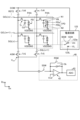
図1は、第1実施形態に係る検出装置を示す平面図である。図1に示すように、検出装置1は、センサ基材21と、センサ部10と、ゲート線駆動回路15と、信号線選択回路16と、検出回路48と、制御回路122と、電源回路123と、第1光源基材51と、第2光源基材52と、第1光源61と、第2光源62と、を有する。第1光源基材51には、複数の第1光源61が設けられる。第2光源基材52には複数の第2光源62が設けられる。
る。複数の第1光源61及び複数の第2光源62は、それぞれ異なる波長の第1光及び第2光を出射する。
又はICの端子数を少なくすることができる。なお、信号線選択回路16は、複数の信号線SGLを束ねて検出回路48に電気的に接続してもよい。
されている。
にバラツキが生じた場合、OPDの特性にバラツキが生じて検出精度が低下する可能性がある。以下、有機半導体層にバラツキが生じた場合の光センサPDのダイオード特性について、図5を参照して説明する。
キにより、OPDの逆方向特性が破線で示したように変化する場合がある。これにより、後述する露光期間(実効露光期間)において光センサPDに流れる逆方向電流が部分検出領域PAAごとにバラツキが生じることとなり、検出精度が低下する。
e(ルブレン:5,6,11,12-tetraphenyltetracene)、PDI(Perylene(ペリレン)の誘導体)等を用いることができる。
3HTとPCBMとが混合した状態の膜、又はF8BTとPDIとが混合した状態の膜とすることができる。
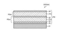
MDPP3TとPCBMとが混合した状態の膜)を用いることができる。この場合、第1フォトダイオードPDaは、可視光(例えば400nm以上650nm以下の波長)に対し感度を有する。第2フォトダイオードPDbは、近赤外光(例えば780nm以上950nm以下の波長)に対し感度を有する。
BMはN型半導体であり、P3HT:PCMBは、P3HTとPCMBとが混合したヘテロジャンクション構成のOPDである。
り、PMDPP3T:PCMBは、PMDPP3TとPCMBとが混合したヘテロジャンクション構成のOPDである。
図14は、第2実施形態に係る検出装置を示す回路図である。なお、以下の説明では、上述した実施形態で説明したものと同じ構成要素には同一の符号を付して重複する説明は省略する。
10 センサ部
11 検出制御部
15 ゲート線駆動回路
16 信号線選択回路
21 センサ基材
31a 第1活性層
31b 第2活性層
32 正孔輸送層
33 電子輸送層
34 上部電極
35 下部電極
40 検出部
48 検出回路
123a 駆動信号供給回路
N1 第1端子
N2 第2端子
PD 光センサ
PDa 第1フォトダイオード
PDb 第2フォトダイオード
VDDSNS 駆動信号
COM 基準電位
VB バイアス電圧
VH 第1電圧信号
VL 第2電圧信号
Claims (5)
- 基板の上に配列された複数の光センサを有する検出装置であって、
複数の前記光センサは、それぞれ、
第1フォトダイオードと、
前記第1フォトダイオードと直列に、かつ、逆方向に接続される第2フォトダイオードと、を有し、
前記第1フォトダイオードが順バイアス駆動され、前記第2フォトダイオードが逆バイアス駆動された場合に、前記第2フォトダイオードが検出し、前記第1フォトダイオードの特性を初期状態に戻すリフレッシュ動作が行われ、
前記第1フォトダイオードが逆バイアス駆動され、前記第2フォトダイオードが順バイアス駆動された場合に、前記第1フォトダイオードが検出し、前記第2フォトダイオードの特性を初期状態に戻すリフレッシュ動作が行われる
検出装置。 - 前記第1フォトダイオードと前記第2フォトダイオードは、光の波長に対して異なる感度特性を有する
請求項1に記載の検出装置。 - 前記第1フォトダイオードは、可視光を検出し、
前記第2フォトダイオードは、近赤外光を検出する
請求項1又は請求項2に記載の検出装置。 - 前記光センサに駆動信号を供給する駆動信号供給回路を有し、
前記駆動信号供給回路は、基準電位よりも高レベル電圧の第1電圧信号と、前記基準電位よりも低レベル電圧の第2電圧信号と、を時分割で前記光センサに供給する
請求項1から請求項3のいずれか1項に記載の検出装置。 - 前記光センサは、前記基板に垂直な方向で、第1電極、電子輸送層、第1活性層、正孔輸送層、第2活性層、第2電極の順に積層される
請求項1から請求項4のいずれか1項に記載の検出装置。
Applications Claiming Priority (3)
| Application Number | Priority Date | Filing Date | Title |
|---|---|---|---|
| JP2021010589 | 2021-01-26 | ||
| JP2021010589 | 2021-01-26 | ||
| PCT/JP2022/002773 WO2022163681A1 (ja) | 2021-01-26 | 2022-01-26 | 検出装置 |
Publications (2)
| Publication Number | Publication Date |
|---|---|
| JPWO2022163681A1 JPWO2022163681A1 (ja) | 2022-08-04 |
| JP7536246B2 true JP7536246B2 (ja) | 2024-08-20 |
Family
ID=82653573
Family Applications (1)
| Application Number | Title | Priority Date | Filing Date |
|---|---|---|---|
| JP2022578436A Active JP7536246B2 (ja) | 2021-01-26 | 2022-01-26 | 検出装置 |
Country Status (4)
| Country | Link |
|---|---|
| US (1) | US12237346B2 (ja) |
| JP (1) | JP7536246B2 (ja) |
| CN (1) | CN116783711A (ja) |
| WO (1) | WO2022163681A1 (ja) |
Families Citing this family (2)
| Publication number | Priority date | Publication date | Assignee | Title |
|---|---|---|---|---|
| JP7746201B2 (ja) * | 2022-03-16 | 2025-09-30 | 株式会社Magnolia White | 検出装置 |
| WO2024195634A1 (ja) * | 2023-03-23 | 2024-09-26 | 株式会社ジャパンディスプレイ | 検出装置 |
Citations (5)
| Publication number | Priority date | Publication date | Assignee | Title |
|---|---|---|---|---|
| WO2009133716A1 (ja) | 2008-04-28 | 2009-11-05 | シャープ株式会社 | ダイオードおよびそれを備えた光センサ回路並びに表示装置 |
| DE102011081564A1 (de) | 2011-08-25 | 2013-02-28 | Ifm Electronic Gmbh | Empfänger für einen optischen Entfernungsmesser |
| US20150129747A1 (en) | 2013-11-12 | 2015-05-14 | Intrinsix Corporation | Stacked photodiode multispectral imager |
| JP2017504979A (ja) | 2014-01-31 | 2017-02-09 | チャンプ グレート インターナショナル コーポレーション | 金属ナノ構造体再結合層を含むタンデム型有機光起電力装置 |
| JP2018116108A (ja) | 2017-01-17 | 2018-07-26 | 株式会社ジャパンディスプレイ | 表示装置 |
Family Cites Families (5)
| Publication number | Priority date | Publication date | Assignee | Title |
|---|---|---|---|---|
| JPH0340574A (ja) * | 1990-07-02 | 1991-02-21 | Canon Inc | 光電変換装置 |
| JP2009032005A (ja) | 2007-07-26 | 2009-02-12 | Toshiba Corp | 入力表示装置および入力表示パネル |
| IL246796B (en) * | 2016-07-14 | 2020-05-31 | Semi Conductor Devices An Elbit Systems Rafael Partnership | A dual band photo-detector and a method thereof |
| CN110323235A (zh) * | 2018-03-29 | 2019-10-11 | 夏普株式会社 | 摄像面板 |
| JPWO2021260494A1 (ja) * | 2020-06-26 | 2021-12-30 |
-
2022
- 2022-01-26 JP JP2022578436A patent/JP7536246B2/ja active Active
- 2022-01-26 CN CN202280011674.4A patent/CN116783711A/zh active Pending
- 2022-01-26 WO PCT/JP2022/002773 patent/WO2022163681A1/ja not_active Ceased
-
2023
- 2023-07-25 US US18/225,809 patent/US12237346B2/en active Active
Patent Citations (5)
| Publication number | Priority date | Publication date | Assignee | Title |
|---|---|---|---|---|
| WO2009133716A1 (ja) | 2008-04-28 | 2009-11-05 | シャープ株式会社 | ダイオードおよびそれを備えた光センサ回路並びに表示装置 |
| DE102011081564A1 (de) | 2011-08-25 | 2013-02-28 | Ifm Electronic Gmbh | Empfänger für einen optischen Entfernungsmesser |
| US20150129747A1 (en) | 2013-11-12 | 2015-05-14 | Intrinsix Corporation | Stacked photodiode multispectral imager |
| JP2017504979A (ja) | 2014-01-31 | 2017-02-09 | チャンプ グレート インターナショナル コーポレーション | 金属ナノ構造体再結合層を含むタンデム型有機光起電力装置 |
| JP2018116108A (ja) | 2017-01-17 | 2018-07-26 | 株式会社ジャパンディスプレイ | 表示装置 |
Also Published As
| Publication number | Publication date |
|---|---|
| WO2022163681A1 (ja) | 2022-08-04 |
| CN116783711A (zh) | 2023-09-19 |
| US12237346B2 (en) | 2025-02-25 |
| US20230369355A1 (en) | 2023-11-16 |
| JPWO2022163681A1 (ja) | 2022-08-04 |
Similar Documents
| Publication | Publication Date | Title |
|---|---|---|
| JP7708400B2 (ja) | 検出装置 | |
| US11687196B2 (en) | Detection device, fingerprint detection device, and vein detection device | |
| JP7529906B2 (ja) | 検出装置 | |
| US20230165019A1 (en) | Detection device | |
| US12514092B2 (en) | Detection device and imaging device | |
| JP7536246B2 (ja) | 検出装置 | |
| US11604543B2 (en) | Detection device | |
| CN116327185A (zh) | 检测装置 | |
| JP7684887B2 (ja) | 検出装置 | |
| JP7530844B2 (ja) | 検出装置 | |
| JP7672302B2 (ja) | 検出システム | |
| JP7614919B2 (ja) | 検出装置 | |
| US20250311524A1 (en) | Detection device | |
| WO2024117209A1 (ja) | 検出装置 | |
| JP2024076578A (ja) | 検出装置 | |
| WO2024195634A1 (ja) | 検出装置 |
Legal Events
| Date | Code | Title | Description |
|---|---|---|---|
| A621 | Written request for application examination |
Free format text: JAPANESE INTERMEDIATE CODE: A621 Effective date: 20230510 |
|
| AA64 | Notification of invalidation of claim of internal priority (with term) |
Free format text: JAPANESE INTERMEDIATE CODE: A241764 Effective date: 20230808 |
|
| A521 | Request for written amendment filed |
Free format text: JAPANESE INTERMEDIATE CODE: A523 Effective date: 20230815 |
|
| A131 | Notification of reasons for refusal |
Free format text: JAPANESE INTERMEDIATE CODE: A131 Effective date: 20240423 |
|
| A521 | Request for written amendment filed |
Free format text: JAPANESE INTERMEDIATE CODE: A523 Effective date: 20240618 |
|
| TRDD | Decision of grant or rejection written | ||
| A01 | Written decision to grant a patent or to grant a registration (utility model) |
Free format text: JAPANESE INTERMEDIATE CODE: A01 Effective date: 20240709 |
|
| A61 | First payment of annual fees (during grant procedure) |
Free format text: JAPANESE INTERMEDIATE CODE: A61 Effective date: 20240726 |
|
| R150 | Certificate of patent or registration of utility model |
Ref document number: 7536246 Country of ref document: JP Free format text: JAPANESE INTERMEDIATE CODE: R150 |