JP7547519B2 - Handheld Electronic Devices - Google Patents

Handheld Electronic Devices Download PDF

Info

Publication number
JP7547519B2
JP7547519B2 JP2023001246A JP2023001246A JP7547519B2 JP 7547519 B2 JP7547519 B2 JP 7547519B2 JP 2023001246 A JP2023001246 A JP 2023001246A JP 2023001246 A JP2023001246 A JP 2023001246A JP 7547519 B2 JP7547519 B2 JP 7547519B2
Authority
JP
Japan
Prior art keywords
display
disposed
area
hole
front cover
Prior art date
Legal status (The legal status is an assumption and is not a legal conclusion. Google has not performed a legal analysis and makes no representation as to the accuracy of the status listed.)
Active
Application number
JP2023001246A
Other languages
Japanese (ja)
Other versions
JP2023101470A (en
Inventor
マシュー ディー. ヒル,
ラザミー プータウォン,
ジュン シック ハム,
ジェームス エー. ベルタン,
ベンジャミン ジェイ. カルマン,
シェリー カオ,
Current Assignee (The listed assignees may be inaccurate. Google has not performed a legal analysis and makes no representation or warranty as to the accuracy of the list.)
Apple Inc
Original Assignee
Apple Inc
Priority date (The priority date is an assumption and is not a legal conclusion. Google has not performed a legal analysis and makes no representation as to the accuracy of the date listed.)
Filing date
Publication date
Application filed by Apple Inc filed Critical Apple Inc
Publication of JP2023101470A publication Critical patent/JP2023101470A/en
Application granted granted Critical
Publication of JP7547519B2 publication Critical patent/JP7547519B2/en
Active legal-status Critical Current
Anticipated expiration legal-status Critical

Links

Images

Classifications

    • GPHYSICS
    • G06COMPUTING OR CALCULATING; COUNTING
    • G06FELECTRIC DIGITAL DATA PROCESSING
    • G06F3/00Input arrangements for transferring data to be processed into a form capable of being handled by the computer; Output arrangements for transferring data from processing unit to output unit, e.g. interface arrangements
    • G06F3/01Input arrangements or combined input and output arrangements for interaction between user and computer
    • G06F3/03Arrangements for converting the position or the displacement of a member into a coded form
    • G06F3/041Digitisers, e.g. for touch screens or touch pads, characterised by the transducing means
    • G06F3/042Digitisers, e.g. for touch screens or touch pads, characterised by the transducing means by opto-electronic means
    • G06F3/0421Digitisers, e.g. for touch screens or touch pads, characterised by the transducing means by opto-electronic means by interrupting or reflecting a light beam, e.g. optical touch-screen
    • GPHYSICS
    • G06COMPUTING OR CALCULATING; COUNTING
    • G06FELECTRIC DIGITAL DATA PROCESSING
    • G06F1/00Details not covered by groups G06F3/00 - G06F13/00 and G06F21/00
    • G06F1/16Constructional details or arrangements
    • G06F1/1613Constructional details or arrangements for portable computers
    • G06F1/1626Constructional details or arrangements for portable computers with a single-body enclosure integrating a flat display, e.g. Personal Digital Assistants [PDAs]
    • GPHYSICS
    • G06COMPUTING OR CALCULATING; COUNTING
    • G06FELECTRIC DIGITAL DATA PROCESSING
    • G06F1/00Details not covered by groups G06F3/00 - G06F13/00 and G06F21/00
    • G06F1/16Constructional details or arrangements
    • G06F1/1613Constructional details or arrangements for portable computers
    • G06F1/1633Constructional details or arrangements of portable computers not specific to the type of enclosures covered by groups G06F1/1615 - G06F1/1626
    • G06F1/1637Details related to the display arrangement, including those related to the mounting of the display in the housing
    • G06F1/1643Details related to the display arrangement, including those related to the mounting of the display in the housing the display being associated to a digitizer, e.g. laptops that can be used as penpads
    • GPHYSICS
    • G06COMPUTING OR CALCULATING; COUNTING
    • G06FELECTRIC DIGITAL DATA PROCESSING
    • G06F1/00Details not covered by groups G06F3/00 - G06F13/00 and G06F21/00
    • G06F1/16Constructional details or arrangements
    • G06F1/1613Constructional details or arrangements for portable computers
    • G06F1/1633Constructional details or arrangements of portable computers not specific to the type of enclosures covered by groups G06F1/1615 - G06F1/1626
    • G06F1/1684Constructional details or arrangements related to integrated I/O peripherals not covered by groups G06F1/1635 - G06F1/1675
    • G06F1/1686Constructional details or arrangements related to integrated I/O peripherals not covered by groups G06F1/1635 - G06F1/1675 the I/O peripheral being an integrated camera
    • GPHYSICS
    • G06COMPUTING OR CALCULATING; COUNTING
    • G06FELECTRIC DIGITAL DATA PROCESSING
    • G06F3/00Input arrangements for transferring data to be processed into a form capable of being handled by the computer; Output arrangements for transferring data from processing unit to output unit, e.g. interface arrangements
    • G06F3/01Input arrangements or combined input and output arrangements for interaction between user and computer
    • G06F3/017Gesture based interaction, e.g. based on a set of recognized hand gestures
    • GPHYSICS
    • G06COMPUTING OR CALCULATING; COUNTING
    • G06FELECTRIC DIGITAL DATA PROCESSING
    • G06F3/00Input arrangements for transferring data to be processed into a form capable of being handled by the computer; Output arrangements for transferring data from processing unit to output unit, e.g. interface arrangements
    • G06F3/01Input arrangements or combined input and output arrangements for interaction between user and computer
    • G06F3/03Arrangements for converting the position or the displacement of a member into a coded form
    • G06F3/041Digitisers, e.g. for touch screens or touch pads, characterised by the transducing means
    • G06F3/044Digitisers, e.g. for touch screens or touch pads, characterised by the transducing means by capacitive means
    • G06F3/0448Details of the electrode shape, e.g. for enhancing the detection of touches, for generating specific electric field shapes, for enhancing display quality
    • GPHYSICS
    • G06COMPUTING OR CALCULATING; COUNTING
    • G06FELECTRIC DIGITAL DATA PROCESSING
    • G06F3/00Input arrangements for transferring data to be processed into a form capable of being handled by the computer; Output arrangements for transferring data from processing unit to output unit, e.g. interface arrangements
    • G06F3/01Input arrangements or combined input and output arrangements for interaction between user and computer
    • G06F3/048Interaction techniques based on graphical user interfaces [GUI]
    • G06F3/0487Interaction techniques based on graphical user interfaces [GUI] using specific features provided by the input device, e.g. functions controlled by the rotation of a mouse with dual sensing arrangements, or of the nature of the input device, e.g. tap gestures based on pressure sensed by a digitiser
    • G06F3/0488Interaction techniques based on graphical user interfaces [GUI] using specific features provided by the input device, e.g. functions controlled by the rotation of a mouse with dual sensing arrangements, or of the nature of the input device, e.g. tap gestures based on pressure sensed by a digitiser using a touch-screen or digitiser, e.g. input of commands through traced gestures
    • GPHYSICS
    • G06COMPUTING OR CALCULATING; COUNTING
    • G06FELECTRIC DIGITAL DATA PROCESSING
    • G06F3/00Input arrangements for transferring data to be processed into a form capable of being handled by the computer; Output arrangements for transferring data from processing unit to output unit, e.g. interface arrangements
    • G06F3/14Digital output to display device ; Cooperation and interconnection of the display device with other functional units
    • HELECTRICITY
    • H04ELECTRIC COMMUNICATION TECHNIQUE
    • H04MTELEPHONIC COMMUNICATION
    • H04M1/00Substation equipment, e.g. for use by subscribers
    • H04M1/02Constructional features of telephone sets
    • H04M1/0202Portable telephone sets, e.g. cordless phones, mobile phones or bar type handsets
    • H04M1/026Details of the structure or mounting of specific components
    • H04M1/0264Details of the structure or mounting of specific components for a camera module assembly
    • HELECTRICITY
    • H04ELECTRIC COMMUNICATION TECHNIQUE
    • H04MTELEPHONIC COMMUNICATION
    • H04M1/00Substation equipment, e.g. for use by subscribers
    • H04M1/02Constructional features of telephone sets
    • H04M1/0202Portable telephone sets, e.g. cordless phones, mobile phones or bar type handsets
    • H04M1/026Details of the structure or mounting of specific components
    • H04M1/0266Details of the structure or mounting of specific components for a display module assembly
    • GPHYSICS
    • G06COMPUTING OR CALCULATING; COUNTING
    • G06FELECTRIC DIGITAL DATA PROCESSING
    • G06F3/00Input arrangements for transferring data to be processed into a form capable of being handled by the computer; Output arrangements for transferring data from processing unit to output unit, e.g. interface arrangements
    • G06F3/01Input arrangements or combined input and output arrangements for interaction between user and computer
    • G06F3/03Arrangements for converting the position or the displacement of a member into a coded form
    • G06F3/041Digitisers, e.g. for touch screens or touch pads, characterised by the transducing means
    • G06F3/0412Digitisers structurally integrated in a display
    • GPHYSICS
    • G06COMPUTING OR CALCULATING; COUNTING
    • G06FELECTRIC DIGITAL DATA PROCESSING
    • G06F3/00Input arrangements for transferring data to be processed into a form capable of being handled by the computer; Output arrangements for transferring data from processing unit to output unit, e.g. interface arrangements
    • G06F3/01Input arrangements or combined input and output arrangements for interaction between user and computer
    • G06F3/03Arrangements for converting the position or the displacement of a member into a coded form
    • G06F3/041Digitisers, e.g. for touch screens or touch pads, characterised by the transducing means
    • G06F3/0416Control or interface arrangements specially adapted for digitisers
    • GPHYSICS
    • G06COMPUTING OR CALCULATING; COUNTING
    • G06FELECTRIC DIGITAL DATA PROCESSING
    • G06F3/00Input arrangements for transferring data to be processed into a form capable of being handled by the computer; Output arrangements for transferring data from processing unit to output unit, e.g. interface arrangements
    • G06F3/01Input arrangements or combined input and output arrangements for interaction between user and computer
    • G06F3/03Arrangements for converting the position or the displacement of a member into a coded form
    • G06F3/041Digitisers, e.g. for touch screens or touch pads, characterised by the transducing means
    • G06F3/044Digitisers, e.g. for touch screens or touch pads, characterised by the transducing means by capacitive means
    • HELECTRICITY
    • H04ELECTRIC COMMUNICATION TECHNIQUE
    • H04MTELEPHONIC COMMUNICATION
    • H04M2250/00Details of telephonic subscriber devices
    • H04M2250/12Details of telephonic subscriber devices including a sensor for measuring a physical value, e.g. temperature or motion
    • HELECTRICITY
    • H04ELECTRIC COMMUNICATION TECHNIQUE
    • H04MTELEPHONIC COMMUNICATION
    • H04M2250/00Details of telephonic subscriber devices
    • H04M2250/22Details of telephonic subscriber devices including a touch pad, a touch sensor or a touch detector

Landscapes

  • Engineering & Computer Science (AREA)
  • Theoretical Computer Science (AREA)
  • General Engineering & Computer Science (AREA)
  • Human Computer Interaction (AREA)
  • Physics & Mathematics (AREA)
  • General Physics & Mathematics (AREA)
  • Computer Hardware Design (AREA)
  • Signal Processing (AREA)
  • Quality & Reliability (AREA)
  • Telephone Set Structure (AREA)
  • Telephone Function (AREA)

Description

(関連出願の相互参照)
本出願は、2022年1月10日に出願された「Handheld Electronic Device」と題された米国仮特許出願第63/298,182号の非仮特許出願であり、その利益を主張し、その開示は、参照によりその全体が本明細書に組み込まれる。
CROSS-REFERENCE TO RELATED APPLICATIONS
This application is a non-provisional patent application of and claims the benefit of U.S. Provisional Patent Application No. 63/298,182, entitled "Handheld Electronic Device," filed on January 10, 2022, the disclosure of which is incorporated herein by reference in its entirety.

本開示の主題は、一般に、ハンドヘルド電子デバイスに関し、より詳細には、モバイル電話機に関する。 The subject matter of this disclosure relates generally to handheld electronic devices, and more particularly to mobile telephones.

現代の民生用電子デバイスは、多くの形状及び形態をとり、多数の用途及び機能を有する。例えば、スマートフォンは、ユーザが電話通信を超えて広がる他の人々と対話するための様々な方法を提供する。そのようなデバイスは、そのような対話を容易にするための多数のシステムを含むことができる。例えば、スマートフォンは、グラフィック出力を提供し、タッチ入力を受け取るためのタッチ感知ディスプレイ、音声及びデータコンテンツを送受信するために他のデバイスと接続するための無線通信システム、写真及びビデオを取り込むためのカメラ等を含むことができる。しかしながら、これらのサブシステムを、毎日の使用に耐えることができるコンパクトで信頼性の高い製品に組み込むことは、様々な技術的課題を提示する。本明細書に記載のシステム及び技術は、広範囲の機能を提供するデバイスを提供しながら、これらの課題の多くに対処し得る。 Modern consumer electronic devices come in many shapes and forms and have numerous uses and functions. Smartphones, for example, offer a variety of ways for users to interact with other people that extend beyond telephone communication. Such devices may include a number of systems to facilitate such interactions. For example, a smartphone may include a touch-sensitive display to provide graphical output and receive touch input, a wireless communication system to connect with other devices to send and receive voice and data content, a camera to capture photographs and videos, and the like. However, incorporating these subsystems into a compact, reliable product that can withstand daily use presents a variety of technical challenges. The systems and techniques described herein may address many of these challenges while providing a device that offers a wide range of functionality.

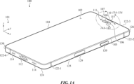
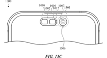
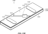
ポータブル電子デバイスは、ハウジング構成要素と、ハウジング構成要素に結合され、ポータブル電子デバイスの前部外面を画定する前部カバーと、を含むエンクロージャを含み得る。ポータブル電子デバイスはまた、前部カバーの下に配置されたディスプレイを含み得、ディスプレイは、アクティブディスプレイ領域と、アクティブディスプレイ領域によって囲まれた第1の穴と、アクティブディスプレイ領域によって囲まれた第2の穴と、を画定する。ポータブル電子デバイスはまた、前部カバーの下かつ第1の穴の下に配置された第1の光学センサと、前部カバーの下かつ第2の穴の下に配置された第2の光学センサと、ディスプレイのアクティブディスプレイ領域内で前部カバーに加えられた第1のタッチ入力と、ディスプレイの第1の穴の上の前部カバーに加えられた第2のタッチ入力とを検出するように構成されたタッチ感知構成要素と、を含んでもよい。 The portable electronic device may include an enclosure including a housing component and a front cover coupled to the housing component and defining a front exterior surface of the portable electronic device. The portable electronic device may also include a display disposed under the front cover, the display defining an active display area, a first hole surrounded by the active display area, and a second hole surrounded by the active display area. The portable electronic device may also include a first optical sensor disposed under the front cover and under the first hole, a second optical sensor disposed under the front cover and under the second hole, and a touch sensing component configured to detect a first touch input applied to the front cover within the active display area of the display and a second touch input applied to the front cover above the first hole of the display.

タッチ感知構成要素は、ディスプレイの第2の穴の上の前部カバーに加えられた第3のタッチ入力を検出するように更に構成され得る。ポータブル電子デバイスは、前部カバーの下かつ第1の穴の下に配置され、物体に光を放射するように構成された発光体を更に含んでもよく、第1の光学センサは、物体から反射された放射された光の一部分を受信するように構成されてもよい。第2のタッチ入力は、第1の光学センサ上で検出されてもよく、タッチ感知構成要素は、発光体上の前部カバーに加えられた第4のタッチ入力を検出するように更に構成されてもよい。 The touch sensing component may be further configured to detect a third touch input applied to the front cover above the second hole of the display. The portable electronic device may further include a light emitter disposed under the front cover and under the first hole and configured to emit light onto an object, and the first optical sensor may be configured to receive a portion of the emitted light reflected from the object. The second touch input may be detected on the first optical sensor, and the touch sensing component may be further configured to detect a fourth touch input applied to the front cover above the light emitter.

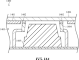
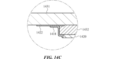
ポータブル電子デバイスはまた、前部カバーの下に配置され、第1の穴の上に配置された第1の開口部、及び第2の穴の上に配置された第2の開口部を画定する不透明マスクを含んでもよい。ポータブル電子デバイスは、前部カバーの内面上に配置されたポリマーコーティング層を更に含んでもよく、不透明マスクは、ポリマーコーティング層上に配置されてもよい。ポリマーコーティング層は、テクスチャ加工表面を画定することができ、不透明マスクは、テクスチャ加工表面上に配置され、テクスチャ加工表面に適合することができる。 The portable electronic device may also include an opaque mask disposed beneath the front cover and defining a first opening disposed over the first hole and a second opening disposed over the second hole. The portable electronic device may further include a polymer coating layer disposed on an inner surface of the front cover, and the opaque mask may be disposed over the polymer coating layer. The polymer coating layer may define a textured surface, and the opaque mask may be disposed over and conform to the textured surface.

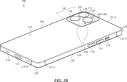
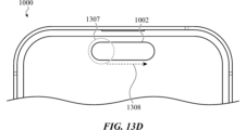
モバイル電話機は、ハウジング構成要素と、ハウジング構成要素に結合され、ディスプレイ領域と、ディスプレイ領域によって囲まれた前向きセンサ領域とを画定する前部カバーと、を含むエンクロージャを含むことができる。ポータブル電子デバイスはまた、前部カバーの下に、グラフィック出力をディスプレイ領域に表示するように構成されたグラフィカルアクティブ領域を画定するディスプレイ層と、グラフィカルアクティブ領域に加えられたタッチ入力を検出するように構成された第1のタッチ感知領域と、前向きセンサ領域のグラフィック非アクティブ領域に加えられたタッチ入力を検出するように構成された第2のタッチ感知領域とを画定するタッチ感知層と、を含むタッチ感知構成要素を含んでもよい。前向きセンサ領域のグラフィック非アクティブ領域に加えられるタッチ入力は、ジェスチャ入力を含み得る。ジェスチャ入力は、スワイプ入力であってもよい。 The mobile telephone may include an enclosure including a housing component and a front cover coupled to the housing component and defining a display area and a forward-facing sensor area surrounded by the display area. The portable electronic device may also include a touch-sensing component below the front cover including a display layer defining a graphically active area configured to display graphical output in the display area, and a touch-sensing layer defining a first touch-sensitive area configured to detect touch input applied to the graphically active area and a second touch-sensitive area configured to detect touch input applied to a graphically inactive area of the forward-facing sensor area. The touch input applied to the graphically inactive area of the forward-facing sensor area may include a gesture input. The gesture input may be a swipe input.

モバイル電話機は、前向きセンサ領域に配置された第1の光学センサと、前向きセンサ領域に配置された第2の光学センサとを更に含んでもよく、タッチ感知構成要素は、第1の光学センサの上に配置された第1の穴と、第2の光学センサの上に配置された第2の穴とを画定してもよい。前向きセンサ領域のグラフィック非アクティブ領域に加えられるタッチ入力は、第1の光学センサ上に加えられる第1のタッチ入力と、第2の光学センサ上に加えられる第2のタッチ入力とを含んでもよい。モバイル電話機は、第1の光学センサ上に加えられた第1のタッチ入力の検出に応じて第1のアクションを実行し、第2の光学センサ上に加えられた第2のタッチ入力の検出に応じて第1のアクションとは異なる第2のアクションを実行するように構成されてもよい。 The mobile phone may further include a first optical sensor disposed in the forward-facing sensor area and a second optical sensor disposed in the forward-facing sensor area, and the touch-sensing component may define a first hole disposed over the first optical sensor and a second hole disposed over the second optical sensor. The touch input applied to the graphically inactive area of the forward-facing sensor area may include a first touch input applied on the first optical sensor and a second touch input applied on the second optical sensor. The mobile phone may be configured to perform a first action in response to detecting the first touch input applied on the first optical sensor and to perform a second action, different from the first action, in response to detecting the second touch input applied on the second optical sensor.

モバイル電話機は、前向きセンサ領域に配置された発光体を更に含んでもよく、タッチ感知構成要素は、発光体の上に配置された第3の穴を画定してもよい。第2のタッチ感知領域の第1の部分は、第1の穴と第2の穴との間に配置されてもよく、第2のタッチ感知領域の第2の部分は、第2の穴と第3の穴との間に配置されてもよい。 The mobile phone may further include a light emitter disposed in the forward-facing sensor area, and the touch sensing component may define a third hole disposed over the light emitter. A first portion of the second touch sensitive area may be disposed between the first hole and the second hole, and a second portion of the second touch sensitive area may be disposed between the second hole and the third hole.

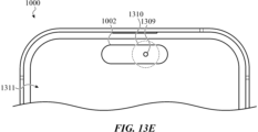
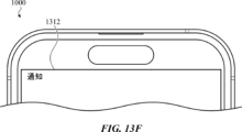
ポータブル電子デバイスは、前部カバーと、前部カバーの第1の領域の下に配置され、前部カバーの第1の領域を介して光を受光するように構成された第1の光学構成要素と、前部カバーの第2の領域の下に配置され、前部カバーの第2の領域を介して光を受光するように構成された第2の光学構成要素と、前部カバーの下に配置されたディスプレイ構成要素と、を含むエンクロージャを含むことができる。ディスプレイ構成要素は、第1の光学構成要素の上に配置された第1の穴と、第2の光学構成要素の上に配置された第2の穴とを画定することができる。ディスプレイ構成要素は、第1の穴及び第2の穴の周りに延在する第1のディスプレイ領域に第1のグラフィック出力を出力し、第1の穴と第2の穴との間に位置する第2のディスプレイ領域に第2のグラフィック出力を出力するように構成されてもよい。第2のグラフィック出力は、ポータブル電子デバイスが通知イベントを受信したことに応じて表示されてもよい。通知イベントを受信する前に、第2のディスプレイ領域はグラフィック出力を表示しなくてもよい。通知イベントを受信する前に、第2のディスプレイ領域は第3のグラフィック出力を表示することができる。ポータブル電子デバイスは、前部カバーの下に配置され、第1の光学構成要素の上に配置された第1の穴と、第2の光学構成要素の上に配置された第2の穴とを画定するタッチ感知構成要素を更に含んでもよい。タッチ感知構成要素は、第1のディスプレイ領域において前部カバーに加えられた入力を検出し、第2のディスプレイ領域において前部カバーに加えられた入力を検出するように構成され得る。 The portable electronic device may include an enclosure including a front cover, a first optical component disposed under a first region of the front cover and configured to receive light through the first region of the front cover, a second optical component disposed under a second region of the front cover and configured to receive light through the second region of the front cover, and a display component disposed under the front cover. The display component may define a first hole disposed over the first optical component and a second hole disposed over the second optical component. The display component may be configured to output a first graphical output to a first display region extending around the first hole and the second hole, and to output a second graphical output to a second display region located between the first hole and the second hole. The second graphical output may be displayed in response to the portable electronic device receiving a notification event. Prior to receiving the notification event, the second display region may not display a graphical output. Prior to receiving the notification event, the second display region may display a third graphical output. The portable electronic device may further include a touch-sensing component disposed beneath the front cover and defining a first hole disposed above the first optical component and a second hole disposed above the second optical component. The touch-sensing component may be configured to detect an input applied to the front cover in the first display area and to detect an input applied to the front cover in the second display area.

モバイル電話機は、ディスプレイと、無線通信回路と、バッテリと、ディスプレイ、無線通信回路、及びバッテリを囲むエンクロージャとを含むことができる。エンクロージャは、透明材料から形成され、モバイル電話機の前部外面を画定する前部カバーと、ガラス材料から形成され、モバイル電話機の後部外面を画定する後部カバーと、モバイル電話機の第1の側部外面を画定する第1の壁部と、第1の側部外面に対向する第2の側部外面を画定する第2の壁部と、第1の壁部と第2の壁部との間に延在する中間シャーシ部とを含む第1のハウジング構成要素と、を含むことができる。エンクロージャは、第1のハウジング構成要素の第1の端部に配置され、第1の外コーナ面を画定する第2のハウジング構成要素と、第1のハウジング構成要素の第1の端部に配置され、第2の外コーナ面を画定する第3のハウジング構成要素と、を更に含んでもよい。 The mobile telephone may include a display, a wireless communication circuit, a battery, and an enclosure surrounding the display, the wireless communication circuit, and the battery. The enclosure may include a first housing component including a front cover formed from a transparent material and defining a front exterior surface of the mobile telephone, a rear cover formed from a glass material and defining a rear exterior surface of the mobile telephone, a first wall portion defining a first side exterior surface of the mobile telephone, a second wall portion defining a second side exterior surface opposite the first side exterior surface, and an intermediate chassis portion extending between the first wall portion and the second wall portion. The enclosure may further include a second housing component disposed at a first end of the first housing component and defining a first exterior corner surface, and a third housing component disposed at the first end of the first housing component and defining a second exterior corner surface.

第1のハウジング構成要素の第1の壁部、第2の壁部、及び中間シャーシ部は、第1の金属材料から一体的に形成されてもよく、第2のハウジング構成要素は、第2の金属材料から形成されてもよく、第3のハウジング構成要素は、第3の金属材料から形成されてもよい。エンクロージャは、第1のハウジング構成要素と第2のハウジング構成要素との間に配置され、第1のポリマー材料から形成された第1の中間要素と、第1のハウジング構成要素と第3のハウジング構成要素との間に配置され、第2のポリマー材料から形成された第2の中間要素と、を更に含んでもよい。第1の壁部、第2の壁部、及び中間シャーシ部は、第1の金属材料の押出成形から一体的に形成されてもよい。 The first wall, the second wall, and the intermediate chassis portion of the first housing component may be integrally formed from a first metallic material, the second housing component may be formed from a second metallic material, and the third housing component may be formed from a third metallic material. The enclosure may further include a first intermediate element disposed between the first housing component and the second housing component and formed from a first polymeric material, and a second intermediate element disposed between the first housing component and the third housing component and formed from a second polymeric material. The first wall, the second wall, and the intermediate chassis portion may be integrally formed from an extrusion of the first metallic material.

無線通信回路は、第2のハウジング構成要素及び第3のハウジング構成要素に動作可能に結合されてもよく、第2及び第3のハウジング構成要素は、無線通信回路用の放射アンテナ要素として動作するように構成されてもよい。ディスプレイは、中間シャーシ部の第1の側部に配置されてもよく、バッテリは、中間シャーシ部の第1の側部に対向する第2の側部に配置されてもよい。 The wireless communication circuitry may be operably coupled to the second and third housing components, and the second and third housing components may be configured to operate as radiating antenna elements for the wireless communication circuitry. The display may be disposed on a first side of the intermediate chassis portion, and the battery may be disposed on a second side opposite the first side of the intermediate chassis portion.

モバイル電話機は、中間シャーシ部に結合された回路基板アセンブリと、回路基板アセンブリを中間シャーシ部に熱的に結合する熱ブリッジと、を更に含むことができる。熱ブリッジは、回路基板アセンブリの第1の側部に近接して配置されてもよく、回路基板アセンブリの第1の側部は、第1のハウジング構成要素の第1の壁部に近接して配置された回路基板アセンブリの第2の側部に対向してもよい。熱ブリッジは、回路基板アセンブリ及び第1のハウジング構成要素の中間シャーシ部に結合されたグラファイト材料を含むことができる。熱ブリッジは、第1の壁部から内側にオフセットされてもよい。 The mobile phone may further include a circuit board assembly coupled to the mid-chassis portion and a thermal bridge thermally coupling the circuit board assembly to the mid-chassis portion. The thermal bridge may be disposed proximate a first side of the circuit board assembly, the first side of the circuit board assembly facing a second side of the circuit board assembly disposed proximate a first wall of the first housing component. The thermal bridge may include a graphite material coupled to the circuit board assembly and the mid-chassis portion of the first housing component. The thermal bridge may be offset inwardly from the first wall.

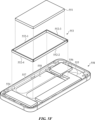
ポータブル電子デバイスは、内部キャビティを画定し、エンクロージャの前部外面を画定する前部カバーアセンブリと、エンクロージャの後部外面を画定する後部カバーアセンブリと、押出金属材料から形成された中間ハウジング構成要素とを含むエンクロージャを含むことができる。中間ハウジング構成要素は、エンクロージャの第1の側部外面を画定する第1の壁部と、第1の側部外面に対向する第2の側部外面を画定する第2の壁部と、第1の壁部及び第2の壁部と一体的に形成され、内部キャビティの少なくとも一部分を画定する中間シャーシ部と、を含むことができる。ポータブル電子デバイスは、エンクロージャの内部キャビティ内に配置され、中間シャーシ部に熱的に結合されたバッテリと、前部カバーアセンブリの下に配置されたディスプレイと、後部カバーアセンブリの下に配置されたカメラアレイと、を更に含んでもよい。 The portable electronic device may include an enclosure that defines an internal cavity and includes a front cover assembly that defines a front exterior surface of the enclosure, a rear cover assembly that defines a rear exterior surface of the enclosure, and an intermediate housing component formed from an extruded metal material. The intermediate housing component may include a first wall that defines a first exterior side surface of the enclosure, a second wall that defines a second exterior side surface opposite the first exterior side surface, and an intermediate chassis portion integrally formed with the first and second walls and that defines at least a portion of the internal cavity. The portable electronic device may further include a battery disposed within the internal cavity of the enclosure and thermally coupled to the intermediate chassis portion, a display disposed below the front cover assembly, and a camera array disposed below the rear cover assembly.

前部カバーアセンブリは、ディスプレイ領域を画定するガラスセラミックシートと、ガラスセラミックシートに結合され、ディスプレイ領域を囲む金属フレームと、を含むことができ、金属フレームは、中間ハウジング構成要素に構造的に結合されたタブのアレイを含む。タブのアレイの第1のタブは、中間ハウジング構成要素に取り付けられた第1のばね結合要素に構造的に結合されてもよく、タブのアレイの第1のタブは、第1のばね結合要素に電気的に結合されてもよい。 The front cover assembly can include a glass-ceramic sheet defining a display area, and a metal frame coupled to the glass-ceramic sheet and surrounding the display area, the metal frame including an array of tabs structurally coupled to an intermediate housing component. A first tab of the array of tabs can be structurally coupled to a first spring coupling element attached to the intermediate housing component, and the first tab of the array of tabs can be electrically coupled to the first spring coupling element.

ポータブル電子デバイスは、ユーザの顔の特徴を検出するように構成された光学顔認識システムを更に含んでもよく、中間シャーシ部は開口部を画定してもよく、光学顔認識システムは、前部カバーアセンブリの下、かつ開口部内に少なくとも部分的に配置されてもよい。中間シャーシ部は、前部カバーアセンブリに面する第1の表面と、第1の表面に対向する第2の表面と、を画定してもよく、光学顔認識システムは、第2の表面に結合されてもよい。エンクロージャは、中間ハウジング構成要素の第1の端部に配置され、第1の外コーナ面を画定する第1のハウジング構成要素と、中間ハウジング構成要素の第1の端部に配置され、第2の外コーナ面を画定する第2のハウジング構成要素と、を更に含んでもよい。 The portable electronic device may further include an optical facial recognition system configured to detect facial features of a user, and the intermediate chassis portion may define an opening, and the optical facial recognition system may be disposed at least partially below the front cover assembly and within the opening. The intermediate chassis portion may define a first surface facing the front cover assembly and a second surface opposite the first surface, and the optical facial recognition system may be coupled to the second surface. The enclosure may further include a first housing component disposed at a first end of the intermediate housing component and defining a first outer corner surface, and a second housing component disposed at the first end of the intermediate housing component and defining a second outer corner surface.

電子デバイスは、第1のガラス材料から形成され、エンクロージャの前部外面を画定する前部カバーと、第2のガラス材料から形成され、エンクロージャの後部外面を画定する後部カバーと、ハウジング構成要素と、を含むエンクロージャを含み得る。ハウジング構成要素は、中間シャーシ部と前部カバーとの間に第1のキャビティを部分的に画定し、中間シャーシ部と後部カバーとの間に第2のキャビティを部分的に画定する中間シャーシ部と、中間シャーシ部の第1の側部に沿って配置され、エンクロージャの第1の側部外面を画定する第1の壁部と、中間シャーシ部の第2の側部に沿って配置され、エンクロージャの第2の側部外面を画定する第2の壁部と、を含むことができる。電子デバイスは、前部カバーに結合されたディスプレイと、第2のキャビティ内に配置され、中間シャーシ部に熱的に結合された回路基板アセンブリと、第2のキャビティ内に配置され、中間シャーシ部に構造的に結合されたバッテリと、を更に含むことができる。第1のガラス材料はガラスセラミック材料であってもよく、第2のガラス材料はアルカリアルミノケイ酸塩材料であってもよい。 The electronic device may include an enclosure including a front cover formed from a first glass material and defining a front exterior surface of the enclosure, a rear cover formed from a second glass material and defining a rear exterior surface of the enclosure, and a housing component. The housing component may include a middle chassis part partially defining a first cavity between the middle chassis part and the front cover and partially defining a second cavity between the middle chassis part and the rear cover, a first wall disposed along a first side of the middle chassis part and defining a first side exterior surface of the enclosure, and a second wall disposed along a second side of the middle chassis part and defining a second side exterior surface of the enclosure. The electronic device may further include a display coupled to the front cover, a circuit board assembly disposed in the second cavity and thermally coupled to the middle chassis part, and a battery disposed in the second cavity and structurally coupled to the middle chassis part. The first glass material may be a glass-ceramic material and the second glass material may be an alkali aluminosilicate material.

中間シャーシ部は、プレート構造と、プレート構造と一体的に形成された取付ボスのアレイとを画定することができ、回路基板アセンブリは、ねじ留め具のセットによって取付ボスのアレイに結合され得る。電子デバイスは、熱伝導性材料から形成された熱ブリッジを更に含んでもよく、熱ブリッジは、回路基板アセンブリと中間シャーシ部との間に配置されてもよい。熱ブリッジは、中間シャーシ部の中央線に近接して配置されてもよい。熱ブリッジは、第1の熱伝導性材料から形成された第1の熱ブリッジであってもよく、電子デバイスは、第2の熱伝導性材料から形成され、回路基板アセンブリと中間シャーシ部との間に配置された第2の熱ブリッジを更に含んでもよい。 The intermediate chassis section may define a plate structure and an array of mounting bosses integrally formed with the plate structure, and the circuit board assembly may be coupled to the array of mounting bosses by a set of screw fasteners. The electronic device may further include a thermal bridge formed from a thermally conductive material, and the thermal bridge may be disposed between the circuit board assembly and the intermediate chassis section. The thermal bridge may be disposed proximate a centerline of the intermediate chassis section. The thermal bridge may be a first thermal bridge formed from a first thermally conductive material, and the electronic device may further include a second thermal bridge formed from a second thermally conductive material and disposed between the circuit board assembly and the intermediate chassis section.

ポータブル電子デバイスは、前部外面を画定する前部カバーと、前部カバーの下に配置され、ディスプレイのグラフィカルアクティブ領域に配置され、第1の複数の透明導電性トレースと、第1の複数の透明導電性トレースに垂直に配向された第2の複数の透明導電性トレースとを含む透明導電性トレースのセットを含むディスプレイと、を含むエンクロージャを含むことができる。ポータブル電子デバイスは、ディスプレイの下にあり、ディスプレイを通って及び前部カバーを通って光を放射するように構成された発光体を含む近接センサと、ディスプレイの下にあり、ディスプレイを通って及び前部カバーを通って、放射された光の反射部分を受信するように構成された光受信器とを更に含んでもよい。発光体は、第1の複数の透明導電性トレース及び第2の複数の透明導電性トレースに対して斜めの方向に沿って光受信器に対して配置されてもよい。 The portable electronic device may include an enclosure including a front cover defining a front exterior surface, and a display disposed below the front cover and including a set of transparent conductive traces disposed in a graphically active area of the display, the set of transparent conductive traces including a first plurality of transparent conductive traces and a second plurality of transparent conductive traces oriented perpendicular to the first plurality of transparent conductive traces. The portable electronic device may further include a proximity sensor below the display and including a light emitter configured to emit light through the display and through the front cover, and a light receiver below the display and configured to receive a reflected portion of the emitted light through the display and through the front cover. The light emitter may be disposed relative to the light receiver along a direction oblique to the first plurality of transparent conductive traces and the second plurality of transparent conductive traces.

近接センサは、前部外面に対する物体の近さを検出するように構成されてもよい。発光体は、約1300ナノメートル~約1400ナノメートルの波長を有する光を放射するように構成されたレーザ発光器であってもよい。ディスプレイは、基板を含んでもよく、第1の複数の透明導電性トレースは、基板上に配置されてもよい。ディスプレイは有機発光ダイオード(OLED)ディスプレイであってもよく、第1の複数の透明導電性トレースはOLEDディスプレイ用のアノードのセットであってもよく、第2の複数の透明導電性トレースはOLEDディスプレイ用のカソードのセットであってもよい。 The proximity sensor may be configured to detect the proximity of an object to the front exterior surface. The light emitter may be a laser emitter configured to emit light having a wavelength between about 1300 nanometers and about 1400 nanometers. The display may include a substrate, and the first plurality of transparent conductive traces may be disposed on the substrate. The display may be an organic light emitting diode (OLED) display, and the first plurality of transparent conductive traces may be a set of anodes for the OLED display, and the second plurality of transparent conductive traces may be a set of cathodes for the OLED display.

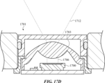
ディスプレイは、タッチセンサを含んでもよく、第1の複数の透明導電性トレースは、タッチセンサ用の第1のセットの電極であってもよく、第2の複数の透明導電性トレースは、タッチセンサ用の第2のセットの電極であってもよい。ディスプレイは、第1の穴及び第2の穴を画定する不透明なバッキング層を含むことができ、発光体は、第1の穴の下に配置されてもよく、光受信器は、第2の穴の下に配置されてもよい。 The display may include a touch sensor, and the first plurality of transparent conductive traces may be a first set of electrodes for the touch sensor, and the second plurality of transparent conductive traces may be a second set of electrodes for the touch sensor. The display may include an opaque backing layer defining a first hole and a second hole, and the light emitter may be disposed under the first hole and the light receiver may be disposed under the second hole.

モバイル電話機は、ハウジング構成要素と、ハウジング構成要素に結合され、ディスプレイ領域と、ディスプレイ領域によって囲まれた前向きセンサ領域とを画定する透明カバーと、を含むエンクロージャを含むことができる。モバイル電話機は、透明カバーの下に、ディスプレイ領域にグラフィック出力を表示するように構成されたグラフィカルアクティブ領域を画定するディスプレイを更に含んでもよい。ディスプレイは、第1の方向に沿って延在する第1のセットの導電性トレースと、第1の方向に垂直な第2の方向に沿って延在する第2のセットの導電性トレースとを含む導電性トレースのグリッドを含むことができる。モバイル電話機は、ディスプレイのグラフィカルアクティブ領域の下に配置され、第1の方向及び第2の方向に対して斜めである第3の方向に沿って配置された1対の光学構成要素を含む近接センサを更に含むことができ、1対の光学構成要素は、ディスプレイを介して光を放射するように構成された発光体と、ディスプレイを介して放射された光の反射部分を受信するように構成された光受信器とを含む。第1のセットの導電性トレース及び第2のセットの導電性トレースの導電性トレースは、光学的に透過性の導電性材料から形成されてもよい。 The mobile phone may include an enclosure including a housing component and a transparent cover coupled to the housing component and defining a display area and a forward-facing sensor area surrounded by the display area. The mobile phone may further include a display defining a graphical active area configured to display a graphical output in the display area below the transparent cover. The display may include a grid of conductive traces including a first set of conductive traces extending along a first direction and a second set of conductive traces extending along a second direction perpendicular to the first direction. The mobile phone may further include a proximity sensor including a pair of optical components disposed below the graphical active area of the display and disposed along a third direction that is oblique to the first direction and the second direction, the pair of optical components including a light emitter configured to emit light through the display and a light receiver configured to receive a reflected portion of the emitted light through the display. The conductive traces of the first set of conductive traces and the second set of conductive traces may be formed from an optically transparent conductive material.

第3の方向は、第1の方向及び第2の方向から45度の方向であってもよい。近接センサは、放射された光の反射部分の特性に少なくとも部分的に基づいて、透明カバーに対する物体の近さを検出するように構成されてもよい。 The third direction may be at 45 degrees from the first direction and the second direction. The proximity sensor may be configured to detect the proximity of an object to the transparent cover based at least in part on a characteristic of the reflected portion of the emitted light.

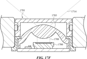
ディスプレイは、第1のサイズを有する第1の穴と、第1のサイズよりも大きい第2のサイズを有する第2の穴とを画定する不透明層を含むことができ、発光体は、第1の穴の下に配置されてもよく、光受信器は、第2の穴の下に配置されてもよい。第2の穴の第1の側部は、第1の方向及び第2の方向に対して斜めである第4の方向に沿って延在してもよく、第2の穴の第2の側部は、第1の方向に対して斜めであり得る第5の方向に沿って延在してもよい。 The display may include an opaque layer defining a first hole having a first size and a second hole having a second size larger than the first size, the light emitter may be disposed under the first hole, and the light receiver may be disposed under the second hole. A first side of the second hole may extend along a fourth direction that is oblique to the first direction and the second direction, and a second side of the second hole may extend along a fifth direction that may be oblique to the first direction.

モバイル電話機は、エンクロージャ内にブラケット構造を更に含み、第3の方向に平行な第4の方向に沿って延在する第1の壁部を画定することができ、近接センサは、第3の方向に平行な第5の方向に沿って延在する第2の壁部を画定するハウジングを含むことができ、第2の壁部は、第1の壁部から間隙によって離間して設定される。 The mobile telephone may further include a bracket structure within the enclosure defining a first wall portion extending along a fourth direction parallel to the third direction, and the proximity sensor may include a housing defining a second wall portion extending along a fifth direction parallel to the third direction, the second wall portion being spaced apart from the first wall portion by a gap.

ポータブル電子デバイスは、前部外面を画定する前部カバーと、前部カバーの下に配置され、1つ以上の電極層を含むディスプレイと、を含むエンクロージャを含むことができる。1つ以上の電極層は、第1の複数の透明導電性トレースと、第1の複数の透明導電性トレースに垂直に配向された第2の複数の透明導電性トレースとを含んでもよい。ディスプレイは、1つ以上の電極層の下に配置され、不透明層を通って延在し、第1の複数の透明導電性トレース及び第2の複数の透明導電性トレースに対して斜めの方向に沿って配向された1対の穴を画定する不透明層を更に含んでもよい。ポータブル電子デバイスは、1対の穴の第1の穴の下に配置され、第1の穴を通して光を放射するように構成された発光体と、1対の穴の第2の穴の下に配置され、発光体によって放射された光の反射部分に少なくとも部分的に基づいて、ポータブル電子デバイスへの物体の近さを検出するように構成された光受信器と、を更に含んでもよい。発光体によって放射される光は、約1300ナノメートル~約1400ナノメートルの波長を有し得る。 The portable electronic device may include an enclosure including a front cover defining a front exterior surface and a display disposed below the front cover and including one or more electrode layers. The one or more electrode layers may include a first plurality of transparent conductive traces and a second plurality of transparent conductive traces oriented perpendicular to the first plurality of transparent conductive traces. The display may further include an opaque layer disposed below the one or more electrode layers and extending through the opaque layer to define a pair of holes oriented along an oblique direction relative to the first plurality of transparent conductive traces and the second plurality of transparent conductive traces. The portable electronic device may further include a light emitter disposed below a first hole of the pair of holes and configured to emit light through the first hole, and a light receiver disposed below a second hole of the pair of holes and configured to detect a proximity of an object to the portable electronic device based at least in part on a reflected portion of the light emitted by the light emitter. The light emitted by the light emitter may have a wavelength of about 1300 nanometers to about 1400 nanometers.

第2の穴は、第1の穴よりも大きくてもよい。第1の複数の透明導電性トレース及び第2の複数の透明導電性トレースの透明導電性トレースは、インジウムスズ酸化物を含むことができる。ディスプレイは有機発光ダイオード(OLED)ディスプレイであってもよく、第1の複数の透明導電性トレースはOLEDディスプレイ用のアノードのセットであってもよく、第2の複数の透明導電性トレースはOLEDディスプレイ用のカソードのセットであってもよい。光受信器は、ディスプレイが第1の穴及び第2の穴の上方でグラフィック出力を生成していることがある間に、ポータブル電子デバイスへの物体の近さを検出するように構成されてもよい。 The second hole may be larger than the first hole. The transparent conductive traces of the first plurality of transparent conductive traces and the second plurality of transparent conductive traces may include indium tin oxide. The display may be an organic light emitting diode (OLED) display, the first plurality of transparent conductive traces may be a set of anodes for the OLED display, and the second plurality of transparent conductive traces may be a set of cathodes for the OLED display. The optical receiver may be configured to detect the proximity of an object to the portable electronic device while the display may be generating a graphical output over the first hole and the second hole.

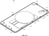
ポータブル電子デバイスは、ポータブル電子デバイスの前部外面を画定する前部カバーと、ポータブル電子デバイスの後部外面を画定する後部カバーと、を含むエンクロージャを含むことができる。ポータブル電子デバイスは、複数の照明可能領域を画定する発光構成要素を含む後向きカメラ及び後向きフラッシュを更に含んでもよい。発光構成要素は、複数の照明可能領域の第1のサブセットを照明して第1の視野を照明し、複数の照明可能領域の第2のサブセットを照明して、第2のサブセットは第1のサブセットとは異なり、第1の視野とは異なる第2の視野を照明するように構成されていてもよい。 The portable electronic device may include an enclosure including a front cover defining a front exterior surface of the portable electronic device and a rear cover defining a rear exterior surface of the portable electronic device. The portable electronic device may further include a rear-facing camera and a rear-facing flash including a light-emitting component defining a plurality of illuminable areas. The light-emitting component may be configured to illuminate a first subset of the plurality of illuminable areas to illuminate a first field of view and to illuminate a second subset of the plurality of illuminable areas to illuminate a second field of view that is different from the first subset and different from the first field of view.

後向きカメラは、第1の視野を有する第1の後向きカメラであってもよく、ポータブル電子デバイスは、第2の視野を有する第2の後向きカメラと、第1の視野とは異なり、第2の視野とは異なる第3の視野を有する第3の後向きカメラと、を更に含んでもよい。発光構成要素は、第1の後向きカメラで第1の画像を取り込みながら第1の視野を照明し、第2の後向きカメラで第2の画像を取り込みながら第2の視野を照明し、複数の照明可能領域の第3のサブセットを照明して、第3のサブセットは第1のサブセット及び第2のサブセットとは異なり、第3の後向きカメラで第3の画像を取り込みながら第3の視野を照明するように構成されてもよい。後向きフラッシュは、発光構成要素の上方に配置されたフラッシュレンズを含んでもよく、複数の照明可能領域の第1のサブセットは、フラッシュレンズの中心の下に配置された第1の照明可能領域であってもよく、複数の照明可能領域の第2のサブセットは、第1の照明可能領域の周囲あたりに配置されてもよく、複数の照明可能領域の第3のサブセットは、第1の照明可能領域の周囲あたりに配置されてもよい。複数の照明可能領域は、グリッドに配置された照明可能領域のアレイを含むことができる。 The rear-facing camera may be a first rear-facing camera having a first field of view, and the portable electronic device may further include a second rear-facing camera having a second field of view, and a third rear-facing camera having a third field of view different from the first field of view and different from the second field of view. The light-emitting component may be configured to illuminate the first field of view while capturing the first image with the first rear-facing camera, illuminate the second field of view while capturing the second image with the second rear-facing camera, illuminate a third subset of the plurality of illuminable areas, the third subset being different from the first and second subsets, and illuminate the third field of view while capturing the third image with the third rear-facing camera. The rear-facing flash may include a flash lens disposed above the light-emitting component, and a first subset of the plurality of illuminable areas may be a first illuminable area disposed below a center of the flash lens, a second subset of the plurality of illuminable areas may be disposed about a perimeter of the first illuminable area, and a third subset of the plurality of illuminable areas may be disposed about a perimeter of the first illuminable area. The plurality of illuminable areas may include an array of illuminable areas arranged in a grid.

後向きフラッシュは、フラッシュレンズと、フラッシュレンズの上のフラッシュ窓とを更に含むことができる。フラッシュ窓は、外側と、フラッシュ窓の外側から視認可能なパターンを生成するように構成された複数のリッジを有する内側とを画定することができる。複数のリッジは、同心リッジであってもよい。複数のリッジのうちのリッジは、第1の角度でフラッシュ窓から延在する第1の側部と、第2の角度でフラッシュ窓から延在する第2の側部とを有するピークによって画定されてもよく、第1の角度及び第2の角度は、同じ大きさ及び反対の符号を有する。 The rear-facing flash may further include a flash lens and a flash window over the flash lens. The flash window may define an exterior and an interior having a plurality of ridges configured to generate a pattern viewable from outside the flash window. The plurality of ridges may be concentric ridges. A ridge of the plurality of ridges may be defined by a peak having a first side extending from the flash window at a first angle and a second side extending from the flash window at a second angle, the first angle and the second angle having the same magnitude and opposite sign.

モバイル電話機は、ディスプレイと、ディスプレイを少なくとも部分的に囲むエンクロージャとを含むことができる。エンクロージャは、ハウジング構成要素と、ハウジング構成要素に結合され、ディスプレイの上に配置された前部カバーと、ハウジング構成要素に結合された後部カバーとを含むことができる。モバイル電話機は、視野を有し、シーンの画像を取り込むように構成された後向きカメラと、シーンを照明するように構成され、発光構成要素を含む後向きフラッシュと、発光構成要素上にあり、発光構成要素によって放射された光を投射して、後向きカメラの視野に対応する光のフラッドを生成するように構成されたレンズと、レンズ上のフラッシュ窓とを更に含むことができる。フラッシュ窓は、外側と、一連の同心円形リッジを有する内側とを画定することができ、一連の同心円形リッジは、フラッシュ窓の内側から延在する対称ピークによって画定されるリッジを含む。エアギャップは、フラッシュ窓とレンズとの間に画定されてもよい。 The mobile phone may include a display and an enclosure at least partially surrounding the display. The enclosure may include a housing component, a front cover coupled to the housing component and disposed over the display, and a rear cover coupled to the housing component. The mobile phone may further include a rear-facing camera having a field of view and configured to capture an image of a scene, a rear-facing flash configured to illuminate the scene and including a light-emitting component, a lens on the light-emitting component and configured to project light emitted by the light-emitting component to generate a flood of light corresponding to the field of view of the rear-facing camera, and a flash window on the lens. The flash window may define an exterior and an interior having a series of concentric circular ridges, the series of concentric circular ridges including ridges defined by symmetrical peaks extending from an interior of the flash window. An air gap may be defined between the flash window and the lens.

対称ピークは、第1の角度でフラッシュ窓の内側から延在する第1の側部と、第2の角度でフラッシュ窓の内側から延在する第2の側部とを有することができ、第1の角度及び第2の角度は同じ大きさ及び反対の符号を有する。リッジは第1のリッジであってもよく、対称ピークは第1の対称ピークであってもよく、一連の同心円形リッジは、フラッシュ窓の内側から延在する第2の対称ピークによって画定される第2のリッジを更に含んでもよく、第2の対称ピークは、第1の角度に等しい第3の角度でフラッシュ窓の内側から延在する第3の側部と、第2の角度に等しい第4の角度でフラッシュ窓の内側から延在する第4の側部とを有する。 The symmetric peak may have a first side extending from the inside of the flash window at a first angle and a second side extending from the inside of the flash window at a second angle, the first angle and the second angle having the same magnitude and opposite sign. The ridge may be a first ridge and the symmetric peak may be a first symmetric peak, and the series of concentric circular ridges may further include a second ridge defined by a second symmetric peak extending from the inside of the flash window, the second symmetric peak having a third side extending from the inside of the flash window at a third angle equal to the first angle and a fourth side extending from the inside of the flash window at a fourth angle equal to the second angle.

モバイル電話機は、フラッシュ本体を更に含んでもよく、フラッシュ窓は、フラッシュ本体の透明部分によって画定されてもよく、フラッシュ本体は、透明部分の下に配置された不透明部分を画定してもよい。フラッシュ本体の不透明部分の一部分は、レンズを通して視認可能であってもよい。フラッシュ本体の透明部分及びフラッシュ本体の不透明部分は、モノリシックポリマー構造の部分であってもよい。 The mobile phone may further include a flash body, and the flash window may be defined by a transparent portion of the flash body, and the flash body may define an opaque portion disposed below the transparent portion. A portion of the opaque portion of the flash body may be viewable through the lens. The transparent portion of the flash body and the opaque portion of the flash body may be part of a monolithic polymer structure.

ポータブル電子デバイスは、ハウジングと、ハウジングに結合され、ポータブル電子デバイスの前面を画定する前部カバーと、ポータブル電子デバイスの後面に沿って配置されたセンサアレイとを含むことができる。センサアレイは、画像を取り込むように構成されたカメラと、照明場を生成するように構成されたフラッシュとを含むことができ、フラッシュは、窓部を画定するフラッシュ本体と、フラッシュ本体に結合された基板と、基板上に配置され、光を放射するように構成された発光構成要素と、窓部の下で、発光構成要素の上に配置されたレンズと、を含む。レンズは、カメラの視野を照明するために、発光構成要素からの光を窓部を通して透過させるように構成されたフラッシュ指向領域と、フラッシュ指向領域を囲み、フラッシュ本体によって反射された光を窓部を通して透過させるように構成された支持領域とを画定することができる。 The portable electronic device may include a housing, a front cover coupled to the housing and defining a front side of the portable electronic device, and a sensor array disposed along a rear side of the portable electronic device. The sensor array may include a camera configured to capture an image and a flash configured to generate an illumination field, the flash including a flash body defining a window, a substrate coupled to the flash body, a light-emitting component disposed on the substrate and configured to emit light, and a lens disposed below the window and above the light-emitting component. The lens may define a flash-directing region configured to transmit light from the light-emitting component through the window to illuminate a field of view of the camera, and a support region surrounding the flash-directing region and configured to transmit light reflected by the flash body through the window.

レンズの支持領域は、フラッシュ本体の窓部に面する外面と、外面に対向する内面とを画定することができ、外面又は内面の少なくとも1つの一部分は、テクスチャ加工表面を有することができる。テクスチャ加工表面は、レンズのフラッシュ指向領域によって画定される表面とは異なる表面テクスチャを有することができる。 The support region of the lens can define an outer surface facing the window portion of the flash body and an inner surface opposite the outer surface, and at least a portion of the outer surface or the inner surface can have a textured surface. The textured surface can have a different surface texture than the surface defined by the flash directing region of the lens.

窓部は、外側及び内側を画定することができる。内側は、窓部の外側から視認可能なパターンを生成するように構成された複数のリッジを有することができ、複数のリッジは、窓部の内側から延在し、対称ピークを画定する一連の同心円形リッジを含むことができる。 The window portion can define an exterior and an interior. The interior portion can have a plurality of ridges configured to generate a pattern visible from outside the window portion, and the plurality of ridges can include a series of concentric circular ridges extending from the interior portion of the window portion and defining a symmetrical peak.

窓部は、フラッシュ本体の透明部分によって画定されてもよく、フラッシュ本体は、透明部分の下に配置された不透明部分を更に画定してもよい。フラッシュ本体によって反射された光は、フラッシュ本体の不透明部分によって反射され得る。 The window may be defined by a transparent portion of the flash body, and the flash body may further define an opaque portion disposed below the transparent portion. Light reflected by the flash body may be reflected by the opaque portion of the flash body.

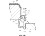
モバイル電話機は、ディスプレイと、ディスプレイを囲み、ディスプレイの上に配置され、前部外面を画定する前部カバーを含むエンクロージャと、後部外面及び後部外面に沿った隆起したセンサアレイ領域を画定する後部カバーとを含むことができる。隆起したセンサアレイ領域は、隆起したセンサアレイ領域を通って延在する第1の穴と、隆起したセンサアレイ領域を通って延在する第2の穴とを画定することができる。第2の穴は、後部カバーの内面に沿った第1の開口部であって、第1の開口サイズを有する第1の開口部と、後部カバーの後部外面に沿った第2の開口部であって、第1の開口サイズよりも小さい第2の開口サイズを有する第2の開口部とによって画定されてもよい。モバイル電話機は、エンクロージャ内に少なくとも部分的にあり、第1の穴内に延在する第1のレンズアセンブリを有する第1のカメラと、エンクロージャ内に少なくとも部分的にあり、第2の穴内に延在する第2のレンズアセンブリを有する第2のカメラと、を更に含んでもよい。第2のレンズアセンブリは、第1の外径を有し、第1の開口部を通って延在するベース部と、第1の外径よりも小さい第2の外径を有し、第2の開口部を通って延在する端部と、を画定することができる。後部カバーは、ガラス材料から形成されてもよい。 The mobile phone may include a display, an enclosure including a front cover surrounding the display and positioned over the display and defining a front exterior surface, and a rear cover defining a rear exterior surface and a raised sensor array area along the rear exterior surface. The raised sensor array area may define a first hole extending through the raised sensor array area and a second hole extending through the raised sensor array area. The second hole may be defined by a first opening along an inner surface of the rear cover, the first opening having a first opening size, and a second opening along a rear exterior surface of the rear cover, the second opening having a second opening size smaller than the first opening size. The mobile phone may further include a first camera at least partially within the enclosure and having a first lens assembly extending into the first hole, and a second camera at least partially within the enclosure and having a second lens assembly extending into the second hole. The second lens assembly can define a base having a first outer diameter and extending through the first opening, and an end having a second outer diameter smaller than the first outer diameter and extending through the second opening. The rear cover can be formed from a glass material.

第2の穴は、第1の開口部に近接するテーパ部と、第2の開口部に近接する円筒部とを有する穴表面によって画定されてもよい。テーパ部は、円錐台形表面を画定することができる。 The second hole may be defined by a hole surface having a tapered portion proximate the first opening and a cylindrical portion proximate the second opening. The tapered portion may define a frustoconical surface.

モバイル電話機は、後部カバーに結合され、第2の穴内に延在するテーパ状壁部を画定するフレーム部材を更に含んでもよく、第2のカメラはフレーム部材に取り付けられてもよい。モバイル電話機は、第2の穴に配置され、フレーム部材に結合されたトリムリングを更に含むことができる。トリムリングは第1のトリムリングであってもよく、モバイル電話機は、第2の穴に配置され、第1のトリムリングに結合された第2のトリムリングを更に含んでもよい。 The mobile phone may further include a frame member coupled to the rear cover and defining a tapered wall portion extending into the second hole, and the second camera may be attached to the frame member. The mobile phone may further include a trim ring disposed in the second hole and coupled to the frame member. The trim ring may be a first trim ring, and the mobile phone may further include a second trim ring disposed in the second hole and coupled to the first trim ring.

第2の穴は、第1の開口部に近接するテーパ部及び第2の開口部に近接する円筒部を有する穴表面によって画定されてもよく、モバイル電話機は、トリムリングと穴表面の円筒部との間に接触して配置された封止部材を更に含んでもよい。モバイル電話機は、穴表面のテーパ部及び穴表面の円筒部に適用される不透明コーティングを更に含んでもよい。 The second hole may be defined by a hole surface having a tapered portion proximate the first opening and a cylindrical portion proximate the second opening, and the mobile phone may further include a sealing member disposed in contact between the trim ring and the cylindrical portion of the hole surface. The mobile phone may further include an opaque coating applied to the tapered portion of the hole surface and the cylindrical portion of the hole surface.

ポータブル電子デバイスは、ディスプレイと、バッテリと、ディスプレイ及びバッテリを囲み、ハウジング構成要素と、ハウジング構成要素に結合され、ポータブル電子デバイスの前部外面を画定する前部カバーと、ハウジング構成要素に結合され、ポータブル電子デバイスの後部外面を画定する後部カバーとを含むエンクロージャと、を含むことができる。ポータブル電子デバイスはまた、カメラブラケットを含む後向きセンサアレイと、カメラブラケットに結合され、第1の視野を有する第1のカメラと、カメラブラケットに結合され、第1の視野とは異なる第2の視野を有する第2のカメラと、カメラブラケットに結合され、第1及び第2の視野とは異なる第3の視野を有する第3のカメラと、を含むことができる。ポータブル電子デバイスはまた、カメラブラケットの第1の側部に沿って配置され、第1の方向に沿ってバッテリに向かってカメラブラケットを付勢するように構成された第1の付勢ばねと、カメラブラケットの第2の側部に沿って配置され、第1の方向を横断する第2の方向に沿ってカメラブラケットを付勢するように構成された第2の付勢ばねと、を含むことができる。 The portable electronic device may include a display, a battery, and an enclosure surrounding the display and the battery, the enclosure including a housing component, a front cover coupled to the housing component and defining a front exterior surface of the portable electronic device, and a rear cover coupled to the housing component and defining a rear exterior surface of the portable electronic device. The portable electronic device may also include a rear-facing sensor array including a camera bracket, a first camera coupled to the camera bracket and having a first field of view, a second camera coupled to the camera bracket and having a second field of view different from the first field of view, and a third camera coupled to the camera bracket and having a third field of view different from the first and second fields of view. The portable electronic device may also include a first biasing spring disposed along a first side of the camera bracket and configured to bias the camera bracket toward the battery along a first direction, and a second biasing spring disposed along a second side of the camera bracket and configured to bias the camera bracket along a second direction transverse to the first direction.

ポータブル電子デバイスは、カメラブラケットの周囲あたりに延在し、カメラブラケットの第1の側部に沿って延在し、カメラブラケットとハウジング構成要素の上側壁との間に配置された第1の壁セグメントと、カメラブラケットの第2の側部に沿って延在し、カメラブラケットとハウジング構成要素の側部側壁との間に配置された第2の壁セグメントと、カメラブラケットの第2の側部に対向する第3側部に沿って延在し、カメラブラケットとバッテリとの間に配置された第3の壁セグメントと、を画定する壁構造を更に含んでもよい。 The portable electronic device may further include a wall structure that defines a first wall segment extending about the periphery of the camera bracket, extending along a first side of the camera bracket and disposed between the camera bracket and an upper wall of the housing component, a second wall segment extending along a second side of the camera bracket and disposed between the camera bracket and a lateral side wall of the housing component, and a third wall segment extending along a third side opposite the second side of the camera bracket and disposed between the camera bracket and the battery.

第1のカメラは、カメラブラケットに結合され、第1のカメラの底部を画定する第1のエンクロージャ構成要素と、第1の継ぎ目で第1のエンクロージャ構成要素に結合され、第1のカメラの上部を画定する第2のエンクロージャ構成要素と、を含む第1のカメラエンクロージャを含むことができる。第2のカメラは、カメラブラケットに結合され、第2のカメラの底部を画定する第3のエンクロージャ構成要素と、第2の継ぎ目で第3のエンクロージャ構成要素に結合され、第2のカメラエンクロージャの上部を画定する第4のエンクロージャ構成要素とを含む第2のカメラエンクロージャを含むことができる。カメラブラケットは、第1のカメラと第2のカメラとの間に配置され、第1の継ぎ目及び第2の継ぎ目の下にあり得る上縁部を有するフランジを画定することができる。第2のエンクロージャ構成要素又は第4のエンクロージャ構成要素の少なくとも1つの一部分は、フランジの上縁部の上に少なくとも部分的に延在してもよい。 The first camera may include a first camera enclosure including a first enclosure component coupled to the camera bracket and defining a bottom of the first camera, and a second enclosure component coupled to the first enclosure component at a first seam and defining a top of the first camera. The second camera may include a second camera enclosure including a third enclosure component coupled to the camera bracket and defining a bottom of the second camera, and a fourth enclosure component coupled to the third enclosure component at a second seam and defining a top of the second camera enclosure. The camera bracket may define a flange disposed between the first camera and the second camera and having an upper edge that may be below the first seam and the second seam. At least one portion of the second enclosure component or the fourth enclosure component may extend at least partially above the upper edge of the flange.

後部カバーは、後部カバーの後向きセンサアレイ領域に、第1の穴、第2の穴、及び第3の穴を画定することができる。第1のカメラの一部分は第1の穴内に延在してもよく、第2のカメラの一部分は第2の穴内に延在してもよく、第3のカメラの一部分は第3の穴内に延在してもよい。ポータブル電子デバイスはまた、後向きセンサアレイ領域の外面に沿って配置され、第1の穴内に延在するトリムアセンブリを含んでもよい。トリムアセンブリは、第1のカメラのレンズ部の周りに延在し、レンズ部に面する第1の表面と、第1の表面に対向し、第1のチャネルを画定する第2の表面とを画定する内側トリムリングと、内側トリムリングの周りに延在し、内側トリムリングの第2の表面に面する第3の表面を画定し、第2のチャネルを画定する外側トリムリングと、を含むことができ、第1及び第2のチャネルは、内側トリムリングと外側トリムリングとの間に中空チャンバを画定する。外側トリムリングは、第3の表面に対向し、トリムアセンブリの周囲外面を画定する第4の表面を更に画定することができる。 The rear cover may define a first hole, a second hole, and a third hole in the rear-facing sensor array area of the rear cover. A portion of the first camera may extend into the first hole, a portion of the second camera may extend into the second hole, and a portion of the third camera may extend into the third hole. The portable electronic device may also include a trim assembly disposed along an outer surface of the rear-facing sensor array area and extending into the first hole. The trim assembly may include an inner trim ring extending around a lens portion of the first camera and defining a first surface facing the lens portion and a second surface opposing the first surface and defining a first channel, and an outer trim ring extending around the inner trim ring and defining a third surface facing the second surface of the inner trim ring and defining the second channel, the first and second channels defining a hollow chamber between the inner trim ring and the outer trim ring. The outer trim ring may further define a fourth surface opposite the third surface and defining an outer peripheral surface of the trim assembly.

第1のカメラの一部分は、ポータブル電子デバイスの後部外面を越えて延在し、ポータブル電子デバイスは、第1のカメラの一部分を囲むトリムリングを更に含んでもよく、トリムリングは、ポータブル電子デバイスの後部外面上に配置された境界面と、第1の表面テクスチャを有する外周面と、境界面から外周面まで延在し、第1の表面テクスチャとは異なる第2の表面テクスチャを有する面取り面と、を画定してもよい。 A portion of the first camera may extend beyond a rear exterior surface of the portable electronic device, and the portable electronic device may further include a trim ring surrounding a portion of the first camera, the trim ring defining a boundary surface disposed on the rear exterior surface of the portable electronic device, an outer periphery having a first surface texture, and a chamfered surface extending from the boundary surface to the outer periphery and having a second surface texture different from the first surface texture.

ポータブル電子デバイスは、ディスプレイと、ディスプレイを囲むエンクロージャと、を含むことができる。エンクロージャは、ハウジング構成要素と、ハウジング構成要素に結合され、ディスプレイの上に配置された前部カバーと、ハウジング構成要素に結合された後部カバーとを含むことができる。ポータブル電子デバイスは、ハウジング構成要素に結合されたカメラブラケットと、第1の視野を有し、カメラブラケットに結合され、それによって第1のカメラをエンクロージャに結合する第1のカメラと、第1の視野とは異なる第2の視野を有し、カメラブラケットに結合され、それによって第2のカメラをエンクロージャに結合する第2のカメラと、カメラブラケットに画定された第1の穴内に延在し、カメラブラケットを第1の方向に付勢するように構成された第1の付勢ばねと、カメラブラケットの第2の穴内に延在し、カメラブラケットを第1の方向とは異なる第2の方向に付勢するように構成された第2の付勢ばねと、を更に含んでもよい。 The portable electronic device may include a display and an enclosure surrounding the display. The enclosure may include a housing component, a front cover coupled to the housing component and disposed over the display, and a rear cover coupled to the housing component. The portable electronic device may further include a camera bracket coupled to the housing component, a first camera having a first field of view and coupled to the camera bracket, thereby coupling the first camera to the enclosure, a second camera having a second field of view different from the first field of view and coupled to the camera bracket, thereby coupling the second camera to the enclosure, a first biasing spring extending into a first hole defined in the camera bracket and configured to bias the camera bracket in a first direction, and a second biasing spring extending into a second hole in the camera bracket and configured to bias the camera bracket in a second direction different from the first direction.

ハウジング構成要素は、ポータブル電子デバイスの第1の側部外面を画定する第1の壁部と、第1の側部外面に対向する第2の側部外面を画定する第2の壁部と、第1の壁部と第2の壁部との間に延在する中間シャーシ部と、を含むことができる。カメラブラケットは、中間シャーシ部に取り付けられてもよい。第1の方向は、ポータブル電子デバイスの上部に向かっていてもよく、第2の方向は、ポータブル電子デバイスの側部であってもよい。カメラブラケットは、第1のカメラを第2のカメラに対して固定位置に維持するように構成されてもよい。 The housing component may include a first wall defining a first exterior side of the portable electronic device, a second wall defining a second exterior side opposite the first exterior side, and an intermediate chassis portion extending between the first and second walls. The camera bracket may be attached to the intermediate chassis portion. The first direction may be toward a top of the portable electronic device and the second direction may be toward a side of the portable electronic device. The camera bracket may be configured to maintain the first camera in a fixed position relative to the second camera.

ポータブル電子デバイスは、ポータブル電子デバイスの側部外面を画定するハウジング構成要素と、ハウジング構成要素に結合され、ポータブル電子デバイスの前部外面を画定する前部カバーアセンブリと、を含むエンクロージャを含み得る。前部カバーアセンブリは、ノッチを画定するカバーを含むことができる。ポータブル電子デバイスは、前部カバーアセンブリの下に配置され、スピーカアセンブリ、すなわちハウジング構成要素とカバーのノッチとの間に画定されたボイドを含むオーディオ通路の端部、から出力されたオーディオを伝達するように構成されたオーディオ通路に結合されたスピーカアセンブリを含んでもよい。 The portable electronic device may include an enclosure including a housing component defining a side exterior surface of the portable electronic device and a front cover assembly coupled to the housing component and defining a front exterior surface of the portable electronic device. The front cover assembly may include a cover defining a notch. The portable electronic device may include a speaker assembly disposed beneath the front cover assembly and coupled to an audio passage configured to convey audio output from the speaker assembly, i.e., an end of the audio passage including a void defined between the housing component and the notch of the cover.

ボイドは、4つの側部のセットによって境界を定められてもよく、カバーは、4つの側部のセットのうちの3つの側部を画定してもよく、ハウジング構成要素の内面は、4つの側部のセットのうちの1つの側部を画定してもよい。ポータブル電子デバイスは、オーディオ通路内に配置されたグレート要素を更に含んでもよく、グレート要素は外向き面を画定してもよく、外向き面は、カバーの厚さよりも大きくてもよい距離だけ前部外面からオフセットされてもよい。グレート要素は、開口部のアレイを画定することができ、開口部のアレイの各開口部は、0.1mm~0.5mmの範囲の幅を有することができる。開口部のアレイの開口部のサブセットの各々は、幅の少なくとも2倍の長さを有する細長い形状を有することができる。グレート要素は、ポリマー材料から成形されてもよい。 The void may be bounded by a set of four sides, the cover may define three of the set of four sides, and the interior surface of the housing component may define one of the set of four sides. The portable electronic device may further include a grate element disposed within the audio passageway, the grate element may define an outwardly facing surface, and the outwardly facing surface may be offset from the front exterior surface by a distance that may be greater than a thickness of the cover. The grate element may define an array of openings, and each opening in the array of openings may have a width in the range of 0.1 mm to 0.5 mm. Each of a subset of the openings in the array of openings may have an elongated shape having a length at least twice its width. The grate element may be molded from a polymeric material.

グレート要素は、フレームと、フレームに取り付けられたスクリーンメッシュとを含むことができる。フレームは、スクリーンメッシュの縁部上にオーバーモールドされてもよく、スクリーンメッシュは、穿孔のアレイを有してもよく、各穿孔は、100ミクロン~200ミクロンの範囲の直径を有してもよい。 The grate element may include a frame and a screen mesh attached to the frame. The frame may be overmolded onto an edge of the screen mesh, and the screen mesh may have an array of perforations, each of which may have a diameter in the range of 100 microns to 200 microns.

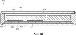
モバイル電話機は、タッチ感知ディスプレイと、タッチ感知ディスプレイを少なくとも部分的に囲むエンクロージャとを含むことができる。エンクロージャは、モバイル電話機の前部外面を画定する透明カバーであって、透明カバーは、縁部に沿って画定された凹部を有する、透明カバーを有する前部カバーアセンブリと、前部カバーアセンブリに結合され、モバイル電話機の上部外面を画定する第1のハウジング構成要素であって、透明カバーの第1のハウジング構成要素及び凹部は、第1のオーディオポートを画定する、第1のハウジング構成要素と、前部カバーアセンブリに結合され、モバイル電話機の下部外面を画定する第2のハウジング構成要素であって、第2のハウジング構成要素は、第2のオーディオポートを画定する、第2のハウジング構成要素と、を含むことができる。モバイル電話機は、前部カバーアセンブリの下に配置され、第1のオーディオポートに音響的に結合されたスピーカアセンブリと、エンクロージャ内に配置され、第2のオーディオポートに音響的に結合されたマイクロフォンと、を更に含むことができる。第1のオーディオポートは、0.5mm未満の幅及び10mm~20mmの範囲の長さを有することができる。 The mobile telephone may include a touch-sensitive display and an enclosure at least partially surrounding the touch-sensitive display. The enclosure may include a front cover assembly having a transparent cover defining a front exterior surface of the mobile telephone, the transparent cover having a recess defined along an edge, a first housing component coupled to the front cover assembly and defining a top exterior surface of the mobile telephone, the first housing component and the recess of the transparent cover defining a first audio port, and a second housing component coupled to the front cover assembly and defining a bottom exterior surface of the mobile telephone, the second housing component defining a second audio port. The mobile telephone may further include a speaker assembly disposed under the front cover assembly and acoustically coupled to the first audio port, and a microphone disposed within the enclosure and acoustically coupled to the second audio port. The first audio port can have a width of less than 0.5 mm and a length in the range of 10 mm to 20 mm.

第1のハウジング構成要素及び透明カバーの凹部は、第1のオーディオポートのボイドを画定することができる。第1のオーディオポートは、オーディオ通路によってスピーカアセンブリに音響的に結合されてもよく、モバイル電話機は、オーディオ通路内に配置されたグレート要素を更に含んでもよい。グレート要素は、ポリマー材料から成形することができ、ポリマー材料は、グレート要素の長さに沿って配置された細長い開口部のセットを画定することができる。グレート要素は、開口部のアレイを画定するスクリーンと、スクリーンの少なくとも1つの縁部に沿って成形されたフレームとを含むことができる。 The first housing component and the recess in the transparent cover may define a first audio port void. The first audio port may be acoustically coupled to the speaker assembly by an audio passageway, and the mobile phone may further include a grate element disposed within the audio passageway. The grate element may be molded from a polymeric material, and the polymeric material may define a set of elongated openings disposed along a length of the grate element. The grate element may include a screen defining an array of openings and a frame molded along at least one edge of the screen.

電子デバイスは、ディスプレイと、オーディオ出力を生成するように構成されたスピーカアセンブリと、ディスプレイ及びスピーカアセンブリを囲むエンクロージャであって、エンクロージャは、電子デバイスの側部外面と、電子デバイスの前部外面の第1の部分とを画定するハウジング構成要素と、ハウジング構成要素に結合され、前部外面の第2の部分を画定する前部カバーアセンブリとを含む、エンクロージャと、を含んでもよい。前部カバーアセンブリは、カバーの縁部に沿ってノッチを画定するカバーを含み、ノッチ及びハウジング構成要素は、スピーカアセンブリに音響的に結合され、オーディオ出力を送信するように構成された開放キャビティを画定してもよい。 The electronic device may include a display, a speaker assembly configured to generate an audio output, and an enclosure surrounding the display and the speaker assembly, the enclosure including a housing component defining a side exterior surface of the electronic device and a first portion of a front exterior surface of the electronic device, and a front cover assembly coupled to the housing component and defining a second portion of the front exterior surface. The front cover assembly may include a cover defining a notch along an edge of the cover, the notch and the housing component defining an open cavity acoustically coupled to the speaker assembly and configured to transmit the audio output.

電子デバイスは、グレート要素を更に含んでもよい。グレート要素は、開放キャビティの下に配置されてもよく、グレート要素は、カバーの厚さよりも大きい距離だけ前部外面から内側にオフセットされてもよい。エンクロージャは、前部外面から内側にオフセットされた内部棚を画定することができ、グレート要素は、内部棚に取り付けられてもよい。グレート要素は、グレート要素の長さに沿って配置されたスリットのアレイを画定することができ、各スリットは、0.1mm~0.5mmの範囲の幅を有することができる。 The electronic device may further include a grate element. The grate element may be disposed below the open cavity, and the grate element may be offset inwardly from the front exterior surface by a distance greater than a thickness of the cover. The enclosure may define an interior shelf offset inwardly from the front exterior surface, and the grate element may be attached to the interior shelf. The grate element may define an array of slits disposed along a length of the grate element, and each slit may have a width in the range of 0.1 mm to 0.5 mm.

電子デバイスはモバイル電話機であってもよく、開放キャビティは、オーディオ出力をユーザの耳に向けるように構成されたモバイル電話機用の受信器ポートを画定してもよい。開放キャビティは、4mm2~8mm2の面積を有する開口部を画定することができる。 The electronic device may be a mobile telephone and the open cavity may define a receiver port for the mobile telephone configured to direct audio output to a user's ear. The open cavity may define an opening having an area between 4 mm2 and 8 mm2.

ポータブル電子デバイスは、前部カバーを有する内部キャビティを画定するエンクロージャと、前部カバーの下に配置されたタッチ感知ディスプレイと、内部キャビティ内に配置され、作動信号に応じてポータブル電子デバイスの外面に沿って触覚出力を生成するように構成された触覚エンジンとを含み得る。触覚エンジンは、触覚エンジンの第1の側部を画定し、第1のばねフレクシャと、第1のばねフレクシャの一部分の上に成形された第1の端部要素とを含む第1の本体構成要素と、触覚エンジンの第1の側部に対向する第2の側部を画定し、第2のばねフレクシャと、第2のばねフレクシャの一部分の上に成形された第2の端部要素とを含む第2の本体構成要素と、第1のばねフレクシャ及び第2のばねフレクシャに結合された可動質量構成要素と、作動信号に応じて可動質量構成要素の直線運動を誘発し、それによって触覚出力を生成するように構成されたコイルと、を含み得る。第1のばねフレクシャは圧縮し得、第2のばねフレクシャは、可動質量構成要素の直線運動の一部分に応じて膨張し得る。 The portable electronic device may include an enclosure defining an internal cavity having a front cover, a touch-sensitive display disposed beneath the front cover, and a haptic engine disposed within the internal cavity and configured to generate a haptic output along an exterior surface of the portable electronic device in response to an actuation signal. The haptic engine may include a first body component defining a first side of the haptic engine and including a first spring flexure and a first end element molded over a portion of the first spring flexure, a second body component defining a second side opposite the first side of the haptic engine and including a second spring flexure and a second end element molded over a portion of the second spring flexure, a movable mass component coupled to the first spring flexure and the second spring flexure, and a coil configured to induce linear motion of the movable mass component in response to an actuation signal, thereby generating a haptic output. The first spring flexure can compress and the second spring flexure can expand in response to a portion of the linear motion of the moving mass component.

第1のばねフレクシャは、第1の端部、第2の端部、及び屈曲部を画定し得、第1の端部要素は、第1のばねフレクシャの第1の端部の上に成形され得、可動質量構成要素は、第1のばねフレクシャの第2の端部に結合され得、屈曲部は、可動質量構成要素の直線運動に応じて変形し得る。可動質量構成要素は、成形ポリマーフレームを含み得、成形ポリマーフレームは、第1のばねフレクシャの第2の端部の上に成形され得、それによって、第1のばねフレクシャを可動質量構成要素に結合し得る。可動質量構成要素は、成形ポリマーフレームに結合され、可動質量構成要素の直線運動を誘導するようにコイルと相互作用するように構成された磁場を生成するように構成された磁石と、成形ポリマーフレームに結合された金属ウェイトと、を更に含み得る。第1の端部要素及び成形ポリマーフレームは、液晶ポリマー材料から形成されてもよい。 The first spring flexure may define a first end, a second end, and a flexure, the first end element may be molded over the first end of the first spring flexure, the mobile mass component may be coupled to the second end of the first spring flexure, and the flexure may deform in response to linear motion of the mobile mass component. The mobile mass component may include a molded polymer frame, the molded polymer frame may be molded over the second end of the first spring flexure, thereby coupling the first spring flexure to the mobile mass component. The mobile mass component may further include a magnet coupled to the molded polymer frame and configured to generate a magnetic field configured to interact with the coil to induce linear motion of the mobile mass component, and a metal weight coupled to the molded polymer frame. The first end element and the molded polymer frame may be formed from a liquid crystal polymer material.

第1の本体構成要素及び第2の本体構成要素は、触覚エンジンの4つの追加の側部の一部分を画定することができる中間本体構成要素に結合されてもよい。第1の本体構成要素及び第2の本体構成要素は、中間本体構成要素に溶接されてもよい。コイルは、中間本体構成要素の内部に結合されてもよい。 The first body component and the second body component may be coupled to an intermediate body component that may define a portion of four additional sides of the haptic engine. The first body component and the second body component may be welded to the intermediate body component. The coil may be coupled to an interior of the intermediate body component.

モバイル電話機は、前部カバーを含むエンクロージャと、エンクロージャ内に少なくとも部分的に配置されたディスプレイと、前部カバーに沿ったタッチ入力を検出するように構成されたタッチセンサと、エンクロージャ内に配置され、タッチ入力に応じて触覚出力を生成するように構成された触覚エンジンと、を含み得る。触覚エンジンは、キャビティを少なくとも部分的に画定する主本体と、主本体の内面に結合されたコイルと、コイルの上に配置された可動質量と、主本体に結合され、第1のばね要素と、第1のばね要素の一部分を密封する第1のポリマー要素とを含む第1の本体構成要素と、主本体に結合され、第2のばね要素と、第2のばね要素の一部分を密封する第2のポリマー要素とを含む第2の本体構成要素と、を含み得、コイルは、可動質量の移動を引き起こし、それによって触覚出力を生成するように構成されていてもよい。 The mobile phone may include an enclosure including a front cover, a display at least partially disposed within the enclosure, a touch sensor configured to detect touch input along the front cover, and a haptic engine disposed within the enclosure and configured to generate a haptic output in response to the touch input. The haptic engine may include a main body at least partially defining a cavity, a coil coupled to an inner surface of the main body, a movable mass disposed above the coil, a first body component coupled to the main body and including a first spring element and a first polymer element sealing a portion of the first spring element, and a second body component coupled to the main body and including a second spring element and a second polymer element sealing a portion of the second spring element, and the coil may be configured to cause movement of the movable mass, thereby generating the haptic output.

第1のばね要素の一部分は、第1のばね要素の第1の端部であり得、第2のばね要素の一部分は、第2のばね要素の第1の端部であり得、可動質量は、第1のばね要素の第2の端部と、第2のばね要素の第2の端部とを密封するフレーム部材を含み得る。第1のポリマー要素は、可動質量の移動中に可動質量の第1の部分に接触して、第1の本体構成要素に向かう可動質量の移動を制限するように構成され得、第2のポリマー要素は、可動質量の移動中に可動質量の第2の部分に接触して、第2の本体構成要素に向かう可動質量の移動を制限するように構成され得る。第1のポリマー要素、第2のポリマー要素、及びフレーム部材は、液晶ポリマー材料から形成され得る。 The portion of the first spring element may be a first end of the first spring element, the portion of the second spring element may be a first end of the second spring element, and the movable mass may include a frame member sealing the second end of the first spring element and the second end of the second spring element. The first polymer element may be configured to contact the first portion of the movable mass during movement of the movable mass to limit movement of the movable mass toward the first body component, and the second polymer element may be configured to contact the second portion of the movable mass during movement of the movable mass to limit movement of the movable mass toward the second body component. The first polymer element, the second polymer element, and the frame member may be formed from a liquid crystal polymer material.

第1の本体構成要素は、第1の金属壁構造を更に含み得、第1のポリマー要素は、第1の金属壁構造に成形され得、第2の本体構成要素は、第2の金属壁構造を更に含み得、第2のポリマー要素は、第2の金属壁構造に成形され得る。主本体は金属構成要素を含み得、第1の金属壁構造は金属構成要素に溶接され得、第2の金属壁構造は、金属構成要素に溶接され得る。 The first body component may further include a first metal wall structure, and the first polymer element may be molded to the first metal wall structure, and the second body component may further include a second metal wall structure, and the second polymer element may be molded to the second metal wall structure. The main body may include a metal component, and the first metal wall structure may be welded to the metal component, and the second metal wall structure may be welded to the metal component.

モバイル電話機は、イベントを検出するように構成されたプロセッサを更に含み得、触覚出力は、イベントの検出に応じて生成され得、触覚出力は、キャビティ内の可動質量の振動を含み得る。 The mobile telephone may further include a processor configured to detect the event, and a haptic output may be generated in response to detecting the event, and the haptic output may include vibration of the movable mass within the cavity.

電子デバイスは、エンクロージャと、エンクロージャ内に少なくとも部分的に配置されたディスプレイと、エンクロージャ内に配置され、電子デバイスの外面に沿って触覚出力を生成するように構成された触覚エンジンと、を含み得る。触覚エンジンは、キャビティを少なくとも部分的に画定する第1のハウジング構成要素と、キャビティ内に配置されたコイルと、キャビティ内に配置された可動質量と、可動質量の第1の端部に結合された第1のフレクシャと、第1のハウジング構成要素に結合され、第1のフレクシャの一部分を少なくとも部分的に密封する第2のハウジング構成要素と、可動質量の第2の端部に結合された第2のフレクシャと、第1のハウジング構成要素に結合され、第2のフレクシャの一部分を少なくとも部分的に密封する第3のハウジング構成要素と、を含み得る。 The electronic device may include an enclosure, a display at least partially disposed within the enclosure, and a haptic engine disposed within the enclosure and configured to generate a haptic output along an exterior surface of the electronic device. The haptic engine may include a first housing component at least partially defining a cavity, a coil disposed within the cavity, a movable mass disposed within the cavity, a first flexure coupled to a first end of the movable mass, a second housing component coupled to the first housing component and at least partially sealing a portion of the first flexure, a second flexure coupled to a second end of the movable mass, and a third housing component coupled to the first housing component and at least partially sealing a portion of the second flexure.

第2のハウジング構成要素は、第1の金属壁構造と、第1の金属壁構造に成形され、第1のフレクシャの一部分を少なくとも部分的に密封する第1のポリマー材料と、を含み得る。第3のハウジング構成要素は、第2の金属壁構造と、第2の金属壁構造に成形され、第2のフレクシャの一部分を少なくとも部分的に密封する第2のポリマー材料と、を含み得る。第1のフレクシャは第1の屈曲板金部材であり得、第2のフレクシャは第2の屈曲板金部材であり得る。第1のフレクシャの一部分は、第1のフレクシャの第1の部分であり、第2のフレクシャの一部分は、第2のフレクシャの第1の部分であり得、可動質量は、第1のフレクシャの第2の部分及び第2のフレクシャの第2の部分を密封するポリマーフレームを含み得る。 The second housing component may include a first metal wall structure and a first polymer material molded to the first metal wall structure and at least partially sealing a portion of the first flexure. The third housing component may include a second metal wall structure and a second polymer material molded to the second metal wall structure and at least partially sealing a portion of the second flexure. The first flexure may be a first bent sheet metal member and the second flexure may be a second bent sheet metal member. The portion of the first flexure may be a first portion of the first flexure and the portion of the second flexure may be a first portion of the second flexure, and the movable mass may include a polymer frame sealing a second portion of the first flexure and a second portion of the second flexure.

モバイル電話機は、ディスプレイと、ディスプレイを囲むエンクロージャであって、ディスプレイの上に配置され、モバイル電話機の前部外面を画定する前部カバーを含む、エンクロージャと、前部カバーに結合され、前部カバーの下のシャーシ部を画定するハウジング構成要素とを含み得る。シャーシ部は、前部カバーに面する第1の側部と、第1の側部に対向し、バッテリ取付領域を画定する第2の側部と、バッテリ取付領域内の第2の側部に沿って形成された第1の凹部と、バッテリ取付領域内の第2の側部に沿って形成された第2の凹部と、を画定することができる。モバイル電話機は、バッテリ取付領域内のシャーシ部に結合されたバッテリと、第1の凹部に配置され、バッテリをシャーシ部に接着する第1の接着剤と、第2の凹部に配置され、バッテリをシャーシ部に接着する第2の接着剤と、を更に含んでもよい。第1及び第2の接着剤は、感圧接着フィルムであってもよい。 The mobile phone may include a display, an enclosure surrounding the display, the enclosure including a front cover disposed over the display and defining a front exterior surface of the mobile phone, and a housing component coupled to the front cover and defining a chassis portion below the front cover. The chassis portion may define a first side facing the front cover, a second side opposite the first side and defining a battery mounting area, a first recess formed along the second side in the battery mounting area, and a second recess formed along the second side in the battery mounting area. The mobile phone may further include a battery coupled to the chassis portion in the battery mounting area, a first adhesive disposed in the first recess and adhering the battery to the chassis portion, and a second adhesive disposed in the second recess and adhering the battery to the chassis portion. The first and second adhesives may be pressure sensitive adhesive films.

第1の凹部及び第2の凹部は、約50~約100ミクロンの凹部深さを有してもよい。第1の接着剤及び第2の接着剤の厚さは、凹部深さよりも約5ミクロン~約30ミクロン大きくてもよい。 The first recess and the second recess may have a recess depth of about 50 to about 100 microns. The thickness of the first adhesive and the second adhesive may be about 5 microns to about 30 microns greater than the recess depth.

バッテリは、長さ軸に沿って第1の距離、及び幅軸に沿って第2の距離だけ延在し得、第1の接着剤は、バッテリの結合側に配置され、長さ軸に沿って延在する接着剤の第1のストリップであり得、第2の接着剤は、バッテリの結合側に配置され、長さ軸に沿って延在する接着剤の第2のストリップであってもよい。第1の接着剤及び第2の接着剤が一緒に、バッテリの結合側の表面積の約60%超を覆ってもよい。第1の接着剤ストリップは、バッテリの結合側の第1の縁部に沿って配置され得、接着剤の第2のストリップは、バッテリの結合側の第2の縁部に沿って配置され得、第2の縁部は第1の縁部に対向しており、グラフィックマーキングは、バッテリの結合側上の接着剤の第1のストリップと接着剤の第2のストリップとの間に配置されてもよい。 The battery may extend a first distance along the length axis and a second distance along the width axis, the first adhesive may be a first strip of adhesive disposed on the mating side of the battery and extending along the length axis, and the second adhesive may be a second strip of adhesive disposed on the mating side of the battery and extending along the length axis. The first adhesive and the second adhesive together may cover more than about 60% of the surface area of the mating side of the battery. The first adhesive strip may be disposed along a first edge of the mating side of the battery, and the second strip of adhesive may be disposed along a second edge of the mating side of the battery, the second edge facing the first edge, and the graphic marking may be disposed between the first strip of adhesive and the second strip of adhesive on the mating side of the battery.

ポータブル電子デバイスは、ディスプレイアセンブリと、バッテリと、バッテリ及びディスプレイアセンブリを囲むエンクロージャであって、ディスプレイアセンブリの上に配置され、ポータブル電子デバイスの前部外面を画定する前部カバーアセンブリと、ポータブル電子デバイスの後部外面を画定する後部カバーアセンブリと、金属材料から形成された中間ハウジング構成要素を含むことができる、エンクロージャとを含み得る。中間ハウジング構成要素は、ポータブル電子デバイスの第1の側部外面を画定する第1の壁部と、第1の側部外面に対向する第2の側部外面を画定する第2の壁部と、第1の壁部及び第2の壁部と一体的に形成された中間シャーシ部と、を含むことができる。中間シャーシ部は、中間シャーシ部の第1の側部に沿って第1の突出部を画定し、中間シャーシ部の第1の側部に対向する第2の側部に沿って第1の凹部であって、バッテリの一部分が第1の凹部内に延在する、第1の凹部を画定する第1の部分と、中間シャーシ部の第2の側部に沿った第2の突出部と、中間シャーシ部の第1の側部に沿った第2の凹部であって、ディスプレイアセンブリの一部分が第2の凹部内に延在する、第2の凹部とを画定する第2の部分と、を画定し得る。 The portable electronic device may include a display assembly, a battery, and an enclosure surrounding the battery and the display assembly, the enclosure being disposed over the display assembly and may include a front cover assembly defining a front exterior surface of the portable electronic device, a rear cover assembly defining a rear exterior surface of the portable electronic device, and an intermediate housing component formed from a metallic material. The intermediate housing component may include a first wall portion defining a first exterior side surface of the portable electronic device, a second wall portion defining a second exterior side surface opposite the first exterior side surface, and an intermediate chassis portion integrally formed with the first wall portion and the second wall portion. The intermediate chassis portion may define a first portion defining a first protrusion along a first side of the intermediate chassis portion and a first recess along a second side opposite the first side of the intermediate chassis portion, with a portion of the battery extending into the first recess, and a second portion defining a second protrusion along the second side of the intermediate chassis portion and a second recess along the first side of the intermediate chassis portion, with a portion of the display assembly extending into the second recess.

ディスプレイアセンブリは、ディスプレイアセンブリの内面に沿って配置された回路要素を含み得、第2の凹部内に延在するディスプレイアセンブリの一部分は、回路要素の一部分であり得る。バッテリは、第3の凹部を画定することができ、中間シャーシ部の第2の側部に沿った第2の突出部は、バッテリによって画定される第3の凹部内に延在し得る。バッテリは、第1の厚さを有するバッテリセル部と、バッテリセル部の側部に沿って配置され、第1の厚さよりも小さい第2の厚さを有するバッテリ回路部と、を含むことができる。バッテリセル部は、中間シャーシ部の第1の部分に取り付けられ得、バッテリ回路部は、第2の突出部の上に配置されていてもよい。接着剤は、第1の凹部内に配置され、バッテリを中間シャーシ部に接着することができる。接着剤の厚さは、第2の凹部の深さよりも約5ミクロン~約20ミクロン大きくてもよい。エアギャップは、中間シャーシ部の第1の部分とディスプレイアセンブリとの間に画定されてもよい。 The display assembly may include a circuit element disposed along an inner surface of the display assembly, and a portion of the display assembly extending into the second recess may be a portion of the circuit element. The battery may define a third recess, and a second protrusion along a second side of the mid-chassis portion may extend into the third recess defined by the battery. The battery may include a battery cell portion having a first thickness and a battery circuit portion disposed along a side of the battery cell portion and having a second thickness less than the first thickness. The battery cell portion may be attached to the first portion of the mid-chassis portion, and the battery circuit portion may be disposed on the second protrusion. An adhesive may be disposed in the first recess and bond the battery to the mid-chassis portion. The thickness of the adhesive may be about 5 microns to about 20 microns greater than the depth of the second recess. An air gap may be defined between the first portion of the mid-chassis portion and the display assembly.

ポータブル電子デバイスは、ディスプレイと、バッテリと、回路基板アセンブリと、ディスプレイ、バッテリ、及び回路基板アセンブリを囲むエンクロージャとを含むことができる。エンクロージャは、ディスプレイの上に配置され得、ポータブル電子デバイスの前部外面を画定する前部カバーと、前部カバーに結合され、ポータブル電子デバイスの側部外面を画定する壁部を含むハウジング構成要素と、を含むことができる。ポータブル電子デバイスは、エンクロージャ内にあり、バッテリの周囲あたりに延在する衝撃バリア構造であって、衝撃バリア構造は、バッテリとハウジング構成要素の壁部との間に配置された第1のバリア部材と、バッテリと回路基板アセンブリとの間に配置された第2のバリア部材と、を更に含み得る。 The portable electronic device may include a display, a battery, a circuit board assembly, and an enclosure surrounding the display, the battery, and the circuit board assembly. The enclosure may be disposed over the display and may include a front cover defining a front exterior surface of the portable electronic device, and a housing component coupled to the front cover and including a wall defining a side exterior surface of the portable electronic device. The portable electronic device may further include an impact barrier structure within the enclosure and extending about a perimeter of the battery, the impact barrier structure including a first barrier member disposed between the battery and the wall of the housing component, and a second barrier member disposed between the battery and the circuit board assembly.

ポータブル電子デバイスは、カメラモジュールを更に含んでもよく、衝撃バリア構造は、バッテリとカメラモジュールとの間に配置された第3のバリア部材を更に含んでもよい。第1のバリア部材、第2のバリア部材、及び第3のバリア部材は、非導電性ポリマー材料から形成されてもよい。第1のバリア部材は、壁部に接着され得、第2のバリア部材は、回路基板アセンブリに接着され得、第3のバリア部材は、カメラモジュールに接着されていてもよい。 The portable electronic device may further include a camera module, and the impact barrier structure may further include a third barrier member disposed between the battery and the camera module. The first barrier member, the second barrier member, and the third barrier member may be formed from a non-conductive polymeric material. The first barrier member may be adhered to the wall portion, the second barrier member may be adhered to the circuit board assembly, and the third barrier member may be adhered to the camera module.

ハウジング構成要素は、前部カバーの下に金属シャーシを更に含み得、第1のバリア部材、第2のバリア部材、及び第3のバリア部材のうちの少なくとも1つは、金属シャーシに結合されていてもよい。第1のバリア部材、第2のバリア部材、及び第3のバリア部材の少なくとも1つは、金属シャーシに溶接されてもよい。 The housing component may further include a metal chassis beneath the front cover, and at least one of the first barrier member, the second barrier member, and the third barrier member may be bonded to the metal chassis. At least one of the first barrier member, the second barrier member, and the third barrier member may be welded to the metal chassis.

モバイル電話機は、内部容積を画定するエンクロージャを含むことができ、エンクロージャは、透明材料から形成され、モバイル電話機の前部外面を画定する前部カバーと、ガラス材料から形成され、モバイル電話機の後部外面を画定する後部カバーと、モバイル電話機の側部外面を画定するハウジング構成要素と、を含み得る。モバイル電話機は、内部容積内に回路基板アセンブリを含み得る。回路基板アセンブリは、回路基板と、回路基板の外面に結合された回路構成要素と、回路基板に結合され、回路構成要素を覆うカウリングと、を含む、回路基板アセンブリを更に含み得、カウリングは約0.5mm未満の厚さを有してもよく、約0.4mm未満の厚さを有するアルミニウム合金から形成されたベース構造と、ベース構造上に位置し、回路基板アセンブリから熱を放散するように構成された熱伝導性構造とを含んでもよい。 The mobile telephone may include an enclosure defining an interior volume, the enclosure may include a front cover formed from a transparent material and defining a front exterior surface of the mobile telephone, a rear cover formed from a glass material and defining a rear exterior surface of the mobile telephone, and a housing component defining a side exterior surface of the mobile telephone. The mobile telephone may include a circuit board assembly within the interior volume. The circuit board assembly may further include a circuit board assembly including a circuit board, circuit components coupled to an exterior surface of the circuit board, and a cowling coupled to the circuit board and covering the circuit components, the cowling may have a thickness of less than about 0.5 mm, and may include a base structure formed from an aluminum alloy having a thickness of less than about 0.4 mm, and a thermally conductive structure located on the base structure and configured to dissipate heat from the circuit board assembly.

アルミニウム合金は、7475系アルミニウム合金であってもよい。熱伝導性構造は、グラファイトを含んでもよい。熱伝導性構造は、複数のグラファイト層、及び複数の接着層を含む多層構造を含み得る。 The aluminum alloy may be a 7475 series aluminum alloy. The thermally conductive structure may include graphite. The thermally conductive structure may include a multi-layer structure including multiple graphite layers and multiple adhesive layers.

熱伝導性構造は、第1の熱伝導性構造であってもよく、カウリングは、回路基板アセンブリの第1の側部に結合されてもよく、回路基板アセンブリは、回路基板アセンブリの第2の側部に配置された第2の熱伝導性構造を更に含んでもよい。エンクロージャは前部カバーアセンブリを含むことができ、前部カバーアセンブリは前部カバーを含むことができ、モバイル電話機は、第1の熱伝導性構造に結合され、回路基板アセンブリを前部カバーアセンブリに熱的に結合する第1の熱ブリッジと、第2の熱伝導性構造に結合され、回路基板アセンブリをエンクロージャの内部構造に熱的に結合する第2の熱ブリッジとを更に含むことができる。 The thermally conductive structure may be a first thermally conductive structure, the cowling may be coupled to a first side of the circuit board assembly, and the circuit board assembly may further include a second thermally conductive structure disposed on a second side of the circuit board assembly. The enclosure may include a front cover assembly, the front cover assembly may include a front cover, and the mobile phone may further include a first thermal bridge coupled to the first thermally conductive structure and thermally coupling the circuit board assembly to the front cover assembly, and a second thermal bridge coupled to the second thermally conductive structure and thermally coupling the circuit board assembly to an internal structure of the enclosure.

カウリングは、カウリングの主要部からカウリングの隆起部まで延在する屈曲セグメントを画定することができ、屈曲セグメントは、約0.5mmより大きくてもよい屈曲半径を有することができる。隆起部におけるカウリングの厚さは、主要部におけるカウリングの厚さよりも小さくてもよい。 The cowling may define a bend segment extending from a main portion of the cowling to a raised portion of the cowling, and the bend segment may have a bend radius that may be greater than about 0.5 mm. The thickness of the cowling at the raised portion may be less than the thickness of the cowling at the main portion.

ポータブル電子デバイスは、エンクロージャであって、ハウジング構造と、ハウジング構造に結合され、ポータブル電子デバイスの前面を画定する第1の透明部材を含む前部カバーアセンブリと、ハウジング構造に結合され、ポータブル電子デバイスの後面を画定する第2の透明部材を含む後部カバーアセンブリとを含むことができる、エンクロージャを含み得る。ポータブル電子デバイスは、少なくとも部分的にエンクロージャ内かつ前部カバーアセンブリの下にあるディスプレイと、少なくとも部分的にエンクロージャ内にあるバッテリと、エンクロージャ内に少なくとも部分的にある回路基板アセンブリと、を更に含んでもよい。回路基板アセンブリは、回路基板と、回路基板に結合され、回路基板アセンブリの外面を画定するカウリングと、を含み得る。カウリングは、アルミニウム合金ベース構造及びアルミニウム合金ベース構造上のグラファイト層を含み得る。アルミニウム合金ベース構造は、7475系アルミニウム合金で形成され得る。アルミニウム合金ベース構造は、約0.4mm未満の厚さを有し得る。 The portable electronic device may include an enclosure that may include a housing structure, a front cover assembly including a first transparent member coupled to the housing structure and defining a front side of the portable electronic device, and a rear cover assembly including a second transparent member coupled to the housing structure and defining a rear side of the portable electronic device. The portable electronic device may further include a display at least partially within the enclosure and below the front cover assembly, a battery at least partially within the enclosure, and a circuit board assembly at least partially within the enclosure. The circuit board assembly may include a circuit board and a cowling coupled to the circuit board and defining an outer surface of the circuit board assembly. The cowling may include an aluminum alloy base structure and a graphite layer on the aluminum alloy base structure. The aluminum alloy base structure may be formed of a 7475 series aluminum alloy. The aluminum alloy base structure may have a thickness of less than about 0.4 mm.

カウリングは、回路基板の上面の実質的に全体を覆うことができる。回路基板アセンブリは、回路基板の上面に結合された第1の回路構成要素と、回路基板の上面に結合された第2の回路構成要素とを含むことができ、カウリングは、第1の回路構成要素及び第2の回路構成要素を覆い得る。 The cowling can cover substantially the entire top surface of the circuit board. The circuit board assembly can include a first circuit component coupled to the top surface of the circuit board and a second circuit component coupled to the top surface of the circuit board, and the cowling can cover the first circuit component and the second circuit component.

グラファイト層は第1のグラファイト層であってもよく、カウリングは回路基板アセンブリの第1の側部に結合されてもよく、回路基板アセンブリは、回路基板アセンブリの第2の側部に結合され、複数の第2のグラファイト層及び複数の接着層を含む多層熱伝導性構造を更に含んでもよい。 The graphite layer may be a first graphite layer, the cowling may be coupled to a first side of the circuit board assembly, and the circuit board assembly may further include a multi-layer thermally conductive structure coupled to a second side of the circuit board assembly and including a plurality of second graphite layers and a plurality of adhesive layers.

回路基板は、第1の回路基板であってもよく、回路基板アセンブリは、第1の回路基板に結合された壁構造と、壁構造に結合され、壁構造によって第1の回路基板の上方に支持された第2の回路基板とを更に含んでもよい。 The circuit board may be a first circuit board, and the circuit board assembly may further include a wall structure coupled to the first circuit board, and a second circuit board coupled to the wall structure and supported above the first circuit board by the wall structure.

電子デバイスは、ディスプレイと、バッテリと、ディスプレイ及びバッテリを囲むエンクロージャとを含むことができる。エンクロージャは、電子デバイスの前部外面を画定する前部カバーアセンブリと、電子デバイスの後部外面を画定する後部カバーアセンブリと、ハウジング構成要素であって、電子デバイスの第1の側部外面を画定する第1の壁部と、第1の側部外面に対向する第2の側部外面を画定する第2の壁部と、第1の壁部と第2の壁部との間に延在する中間シャーシ部と、を含む、ハウジング構成要素と、を含むことができる。電子デバイスは、中間シャーシ部に結合され、ハウジング構成要素の第1の壁部に近接する第1の外周側と、第1の外周側に対向する第2の外周側とを画定する回路基板アセンブリと、回路基板アセンブリを中間シャーシ部に熱的に結合する熱ブリッジであって、熱ブリッジは、回路基板アセンブリの第1の外周側に近接して配置される、熱ブリッジと、を更に含み得る。 The electronic device may include a display, a battery, and an enclosure surrounding the display and the battery. The enclosure may include a front cover assembly defining a front exterior surface of the electronic device, a rear cover assembly defining a rear exterior surface of the electronic device, and a housing component including a first wall defining a first side exterior surface of the electronic device, a second wall defining a second side exterior surface opposite the first side exterior surface, and an intermediate chassis portion extending between the first wall portion and the second wall portion. The electronic device may further include a circuit board assembly coupled to the intermediate chassis portion and defining a first outer perimeter side proximate the first wall portion of the housing component and a second outer perimeter side opposite the first outer perimeter side, and a thermal bridge thermally coupling the circuit board assembly to the intermediate chassis portion, the thermal bridge being disposed proximate the first outer perimeter side of the circuit board assembly.

熱ブリッジの中心は、回路基板アセンブリの中央線からオフセットされてもよい。熱ブリッジは、第1の熱ブリッジであってもよく、電子デバイスは、回路基板アセンブリを前部カバーアセンブリに熱的に結合する第2の熱ブリッジを更に含んでもよい。 The center of the thermal bridge may be offset from a centerline of the circuit board assembly. The thermal bridge may be a first thermal bridge, and the electronic device may further include a second thermal bridge thermally coupling the circuit board assembly to the front cover assembly.

熱ブリッジは、第1の熱ブリッジであってもよく、回路基板アセンブリは、バッテリの第1の側部に沿って延在する第1のセグメントと、バッテリの第2の側部であって、第2の側部は第1の側部に垂直である、第2の側部に沿って延在する第2のセグメントと、を画定してもよい。第1の熱ブリッジは、回路基板アセンブリの第1のセグメント上に配置されてもよく、電子デバイスは、回路基板アセンブリの第2のセグメント上に配置された第2の熱ブリッジを更に含んでもよい。回路基板アセンブリは、回路基板アセンブリの第1のセグメントに結合され、回路基板アセンブリの第1の回路構成要素を覆う第1のカウリングと、回路基板アセンブリの第2のセグメントに結合され、回路基板アセンブリの第2の回路構成要素を覆う第2のカウリングと、第1のカウリング及び第2のカウリングの両方の上に延在する熱伝導性構造とを更に含んでもよく、第1の熱ブリッジ及び第2の熱ブリッジは、熱伝導性構造に結合されてもよい。 The thermal bridge may be a first thermal bridge, and the circuit board assembly may define a first segment extending along a first side of the battery and a second segment extending along a second side of the battery, the second side being perpendicular to the first side. The first thermal bridge may be disposed on the first segment of the circuit board assembly, and the electronic device may further include a second thermal bridge disposed on the second segment of the circuit board assembly. The circuit board assembly may further include a first cowling coupled to the first segment of the circuit board assembly and covering a first circuit component of the circuit board assembly, a second cowling coupled to the second segment of the circuit board assembly and covering a second circuit component of the circuit board assembly, and a thermally conductive structure extending over both the first cowling and the second cowling, and the first thermal bridge and the second thermal bridge may be coupled to the thermally conductive structure.

同様の参照番号が同様の構造的要素を指定する添付図面と共に、以下の詳細な説明によって開示が容易に理解されよう。 The disclosure will be readily understood by the following detailed description when taken in conjunction with the accompanying drawings, in which like reference numbers designate like structural elements.

例示的な電子デバイスを示す。1 illustrates an exemplary electronic device. 例示的な電子デバイスを示す。1 illustrates an exemplary electronic device.

別の例示的な電子デバイスを示す。2 illustrates another exemplary electronic device. 別の例示的な電子デバイスを示す。2 illustrates another exemplary electronic device.

例示的な電子デバイスの分解図である。FIG. 2 is an exploded view of an exemplary electronic device.

例示的な電子デバイスの分解図である。FIG. 2 is an exploded view of an exemplary electronic device.

例示的な電子デバイスの部分分解図である。FIG. 2 is a partially exploded view of an exemplary electronic device.

図4Aの電子デバイスの一部分の分解図を示す。4B shows an exploded view of a portion of the electronic device of FIG. 4A.

例示的な電子デバイスの部分断面図である。1 is a partial cross-sectional view of an exemplary electronic device.

電子デバイス用の例示的な回路基板アセンブリを示す。1 illustrates an exemplary circuit board assembly for an electronic device. 電子デバイス用の例示的な回路基板アセンブリを示す。1 illustrates an exemplary circuit board assembly for an electronic device.

例示的な電子デバイスを示す。1 illustrates an exemplary electronic device.

例示的な電子デバイスの部分断面図である。1 is a partial cross-sectional view of an exemplary electronic device.

例示的な電子デバイスの部分断面図である。1 is a partial cross-sectional view of an exemplary electronic device.

例示的な電子デバイスの部分分解図である。FIG. 2 is a partially exploded view of an exemplary electronic device.

電子デバイス用の例示的な後部カバーアセンブリを示す図である。1 illustrates an exemplary back cover assembly for an electronic device.

電子デバイス用のばねクリップシステムを示す図である。1 illustrates a spring clip system for an electronic device.

電子デバイスのカメラ領域の一部分を示す図である。FIG. 2 illustrates a portion of the camera area of an electronic device. 電子デバイスのカメラ領域の一部分を示す図である。FIG. 2 illustrates a portion of the camera area of an electronic device.

電子デバイスのカメラ領域の部分断面図である。FIG. 2 is a partial cross-sectional view of a camera area of an electronic device.

電子デバイスのカメラ領域の部分断面図である。FIG. 2 is a partial cross-sectional view of a camera area of an electronic device.

電子デバイス用の例示的なトリムアセンブリの部分断面図である。1 is a partial cross-sectional view of an exemplary trim assembly for an electronic device. 電子デバイス用の例示的なトリムアセンブリの部分断面図である。1 is a partial cross-sectional view of an exemplary trim assembly for an electronic device. 電子デバイス用の例示的なトリムアセンブリの部分断面図である。1 is a partial cross-sectional view of an exemplary trim assembly for an electronic device. 電子デバイス用の例示的なトリムアセンブリの部分断面図である。1 is a partial cross-sectional view of an exemplary trim assembly for an electronic device. 電子デバイス用の例示的なトリムアセンブリの部分断面図である。1 is a partial cross-sectional view of an exemplary trim assembly for an electronic device. 電子デバイス用の例示的なトリムアセンブリの部分断面図である。1 is a partial cross-sectional view of an exemplary trim assembly for an electronic device.

別の例示的な電子デバイスのカメラ領域を示す図である。FIG. 2 illustrates a camera area of another exemplary electronic device.

例示的な電子デバイスの一部分を示す図である。FIG. 1 illustrates a portion of an exemplary electronic device.

電子デバイスの近接センサを示す図である。FIG. 1 illustrates a proximity sensor of an electronic device.

例示的な電子デバイスの前向きセンサ領域の部分分解図である。FIG. 2 is a partial exploded view of a forward-facing sensor area of an exemplary electronic device.

例示的な前向きセンサ領域の部分断面図である。FIG. 13 is a partial cross-sectional view of an exemplary forward-facing sensor area. 例示的な前向きセンサ領域の部分断面図である。FIG. 13 is a partial cross-sectional view of an exemplary forward-facing sensor area. 例示的な前向きセンサ領域の部分断面図である。FIG. 13 is a partial cross-sectional view of an exemplary forward-facing sensor area. 例示的な前向きセンサ領域の部分断面図である。FIG. 13 is a partial cross-sectional view of an exemplary forward-facing sensor area.

電子デバイスの例示的な前向きセンサ領域を示す。1 illustrates an exemplary forward-facing sensor area of an electronic device. 電子デバイスの例示的な前向きセンサ領域を示す。1 illustrates an exemplary forward-facing sensor area of an electronic device. 電子デバイスの例示的な前向きセンサ領域を示す。1 illustrates an exemplary forward-facing sensor area of an electronic device. 電子デバイスの例示的な前向きセンサ領域を示す。1 illustrates an exemplary forward-facing sensor area of an electronic device.

例示的な前向きセンサ領域の部分断面図である。FIG. 13 is a partial cross-sectional view of an exemplary forward-facing sensor area. 例示的な前向きセンサ領域の部分断面図である。FIG. 13 is a partial cross-sectional view of an exemplary forward-facing sensor area. 例示的な前向きセンサ領域の部分断面図である。FIG. 13 is a partial cross-sectional view of an exemplary forward-facing sensor area. 例示的な前向きセンサ領域の部分断面図である。FIG. 13 is a partial cross-sectional view of an exemplary forward-facing sensor area.

例示的なディスプレイ層の部分断面図である。FIG. 2 is a partial cross-sectional view of an exemplary display layer. 例示的なディスプレイ層の部分断面図である。FIG. 2 is a partial cross-sectional view of an exemplary display layer.

前向きセンサ領域における例示的なタッチ入力及びグラフィック出力を示す図である。FIG. 1 illustrates an exemplary touch input and graphical output in a forward-facing sensor area. 前向きセンサ領域における例示的なタッチ入力及びグラフィック出力を示す図である。FIG. 13 illustrates an exemplary touch input and graphical output in a forward-facing sensor area. 前向きセンサ領域における例示的なタッチ入力及びグラフィック出力を示す図である。FIG. 13 illustrates an exemplary touch input and graphical output in a forward-facing sensor area. 前向きセンサ領域における例示的なタッチ入力及びグラフィック出力を示す図である。FIG. 1 illustrates an exemplary touch input and graphical output in a forward-facing sensor area. 前向きセンサ領域における例示的なタッチ入力及びグラフィック出力を示す図である。FIG. 13 illustrates an exemplary touch input and graphical output in a forward-facing sensor area. 前向きセンサ領域における例示的なタッチ入力及びグラフィック出力を示す図である。FIG. 1 illustrates an exemplary touch input and graphical output in a forward-facing sensor area.

電子デバイス用の例示的な前向きカメラの部分断面図である。1 is a partial cross-sectional view of an exemplary front-facing camera for an electronic device. 電子デバイス用の例示的な前向きカメラの部分断面図である。1 is a partial cross-sectional view of an exemplary front-facing camera for an electronic device.

電子デバイス用の例示的な前向きセンサ領域の部分断面図である。1 is a partial cross-sectional view of an exemplary forward-facing sensor area for an electronic device. 電子デバイス用の例示的な前向きセンサ領域の部分断面図である。1 is a partial cross-sectional view of an exemplary forward-facing sensor area for an electronic device. 電子デバイス用の例示的な前向きセンサ領域の部分断面図である。1 is a partial cross-sectional view of an exemplary forward-facing sensor area for an electronic device.

例示的な電子デバイスのスピーカ構成の部分図である。FIG. 2 is a partial view of a speaker configuration of an exemplary electronic device.

スピーカ開口部の例示的な構成を示す、例示的な電子デバイスの部分断面図である。1 is a partial cross-sectional view of an exemplary electronic device illustrating an exemplary configuration of speaker openings.

スピーカ開口部の例示的な構成を示す、別の例示的な電子デバイスの部分断面図である。1 is a partial cross-sectional view of another exemplary electronic device illustrating an exemplary configuration of speaker openings.

電子デバイスの例示的な音響カバー構造を示す図である。1A-1C illustrate exemplary acoustic cover structures for electronic devices.

図15Dの音響カバー構造を有する電子デバイスの部分断面図である。FIG. 15E is a partial cross-sectional view of an electronic device having the acoustic cover structure of FIG. 15D.

電子デバイスの別の例示的な音響カバー構造を示す図である。1 illustrates another exemplary acoustic cover structure for an electronic device.

異なる視野を照明するフラッシュモジュールを示す図である。FIG. 1 shows a flash module illuminating different fields of view.

フラッシュモジュールの部分断面図を示す。1 shows a partial cross-sectional view of a flash module. フラッシュモジュールの部分断面図を示す。1 shows a partial cross-sectional view of a flash module.

フラッシュモジュールの発光構造の例示的な照明パターンを示す図である。2A and 2B are diagrams illustrating exemplary illumination patterns of the light-emitting structure of the flash module. フラッシュモジュールの発光構造の例示的な照明パターンを示す図である。2A and 2B are diagrams illustrating exemplary illumination patterns of the light-emitting structure of the flash module. フラッシュモジュールの発光構造の例示的な照明パターンを示す図である。2A and 2B are diagrams illustrating exemplary illumination patterns of the light-emitting structure of the flash module. フラッシュモジュールの発光構造の例示的な照明パターンを示す図である。2A and 2B are diagrams illustrating exemplary illumination patterns of the light-emitting structure of the flash module. フラッシュモジュールの発光構造の例示的な照明パターンを示す図である。2A and 2B are diagrams illustrating exemplary illumination patterns of the light-emitting structure of the flash module. フラッシュモジュールの発光構造の例示的な照明パターンを示す図である。2A and 2B are diagrams illustrating exemplary illumination patterns of the light-emitting structure of the flash module.

フラッシュモジュールの窓部の例示的な構成を示す図である。1A-1C show exemplary configurations of a window portion of a flash module.

図18Aの窓部の部分断面図である。FIG. 18B is a partial cross-sectional view of the window portion of FIG. 18A.

例示的な触覚エンジンの部分分解図である。FIG. 2 is a partial exploded view of an example haptic engine.

図19Aの触覚エンジンの上面図である。FIG. 19B is a top view of the haptic engine of FIG. 19A.

電子デバイス用の例示的な統合モジュールを示す図である。FIG. 1 illustrates an exemplary integrated module for an electronic device.

図20Aの統合モジュールの部分分解図である。FIG. 20B is a partially exploded view of the integrated module of FIG. 20A.

統合モジュールを有するデバイスの部分分解図である。FIG. 1 is a partial exploded view of a device having an integrated module.

スクリーンカバーを有するデバイスの部分分解図である。FIG. 2 is a partial exploded view of a device having a screen cover.

例示的なスクリーンカバーの側部図を示す。1 illustrates a side view of an exemplary screen cover.

例示的なスクリーンプロテクタの部分断面図である。1 is a partial cross-sectional view of an exemplary screen protector. 例示的なスクリーンプロテクタの部分断面図である。1 is a partial cross-sectional view of an exemplary screen protector.

例示的な回路基板アセンブリの部分分解図である。FIG. 2 is a partially exploded view of an exemplary circuit board assembly.

図22Aの回路基板アセンブリの底側図を示す。FIG. 22B shows a bottom view of the circuit board assembly of FIG.

回路基板アセンブリのためのカウリングの部分断面図である。FIG. 2 is a partial cross-sectional view of a cowling for a circuit board assembly. 回路基板アセンブリのためのカウリングの部分断面図である。FIG. 2 is a partial cross-sectional view of a cowling for a circuit board assembly.

例示的な電子デバイスの概略図である。1 is a schematic diagram of an exemplary electronic device.

ここで、添付図面に図示される代表的な実施形態が詳細に説明される。以下の説明は、これらの実施形態を1つの好ましい実施形態に限定することを意図するものではないことを理解されたい。反対に、以下の説明は、添付の特許請求の範囲により定義される記載された実施形態の趣旨及び範囲に含むことができるような、代替形態、修正形態及び均等物を包含することを意図している。 Representative embodiments as illustrated in the accompanying drawings will now be described in detail. It should be understood that the following description is not intended to limit these embodiments to one preferred embodiment. On the contrary, the following description is intended to cover alternatives, modifications, and equivalents as may be included within the spirit and scope of the described embodiments as defined by the appended claims.

本明細書に記載のモバイル電話機は、多数の機能を容易にする複雑で洗練された構成要素及びシステムを含むことができる。例えば、本開示によるモバイル電話機は、タッチ及び/又は力感知ディスプレイ、多数のカメラ(前向き及び後向きカメラの両方を含む)、GPSシステム、触覚アクチュエータ、無線充電システム、並びに、これら(及び他)のシステムを動作させ、そうでなければモバイル電話機の機能を提供するための全ての必要なコンピューティング構成要素及びソフトウェアを含むことができる。 The mobile telephones described herein can include complex and sophisticated components and systems that facilitate numerous functions. For example, a mobile telephone according to the present disclosure can include a touch and/or force sensitive display, multiple cameras (including both front and rear facing cameras), a GPS system, haptic actuators, a wireless charging system, and all necessary computing components and software to operate these (and other) systems and otherwise provide the functionality of the mobile telephone.

図1A及び図1Bは、モバイル電話機として具現化された例示的な電子デバイス100を示す。図1Aはデバイス100の前面を示し、図1Bはデバイスの後側を示す。デバイス100はモバイル電話機であるが、本明細書に提示される概念は、ポータブル電子デバイス、ウェアラブルデバイス(例えば、ウォッチ)、ラップトップコンピュータ、ハンドヘルドゲーミングデバイス、タブレットコンピュータ、コンピューティング周辺機器(例えば、マウス、タッチパッド、キーボード)、又は任意の他のデバイスを含む任意の適切な電子デバイスに適用することができる。したがって、「電子デバイス」への言及は、上記のいずれか及び全てを包含する。 1A and 1B illustrate an exemplary electronic device 100 embodied as a mobile phone. FIG. 1A illustrates the front side of device 100, and FIG. 1B illustrates the back side of the device. Although device 100 is a mobile phone, the concepts presented herein may be applied to any suitable electronic device, including a portable electronic device, a wearable device (e.g., a watch), a laptop computer, a handheld gaming device, a tablet computer, a computing peripheral (e.g., a mouse, touchpad, keyboard), or any other device. Thus, reference to an "electronic device" encompasses any and all of the above.

電子デバイス100は、ハウジング104(1つ以上のハウジング構成要素によって画定されるハウジング構造を含むことができる)に取り付けられたカバー102(例えば、前部カバー)を含む。カバー102は、ディスプレイ103の上に配置されてもよい。カバー102は、透明又は光学的に透過性の材料から形成されるか、又はそれを含むシート又はシート状構造であってもよい。場合によっては、カバー102はガラス材料から形成されるか、又はそれを含み、したがってガラスカバー部材と呼ばれることがある。ガラス材料は、シリカ系ガラス材料、アルミノケイ酸塩ガラス、ボロアルミノケイ酸塩ガラス、アルカリ金属アルミノケイ酸塩ガラス(例えば、リチウムアルミノケイ酸塩ガラス)、又は化学強化ガラスであってもよい。カバー102の他の例示的な材料には、サファイア、セラミック、ガラスセラミック、結晶性ガラス材料、又はプラスチック(例えば、ポリカーボネート)が含まれるが、これらに限定されない。ガラスセラミック材料は、アルミノケイ酸塩ガラスセラミック材料又はボロアルミノケイ酸塩ガラスセラミック材料等のシリカ系ガラスセラミック材料であってもよい。ガラスセラミック材料は、イオン交換によって化学的に強化されてもよい。カバー102は、モノリシック又は単一シートとして形成されてもよい。カバー102はまた、異なる材料、コーティング、及び他の要素の複数の層の複合体として形成されてもよい。 The electronic device 100 includes a cover 102 (e.g., a front cover) attached to a housing 104 (which may include a housing structure defined by one or more housing components). The cover 102 may be disposed over a display 103. The cover 102 may be a sheet or sheet-like structure formed from or including a transparent or optically transmissive material. In some cases, the cover 102 may be formed from or include a glass material and thus may be referred to as a glass cover member. The glass material may be a silica-based glass material, an aluminosilicate glass, a boroaluminosilicate glass, an alkali metal aluminosilicate glass (e.g., lithium aluminosilicate glass), or a chemically strengthened glass. Other exemplary materials for the cover 102 include, but are not limited to, sapphire, ceramic, glass ceramic, a crystalline glass material, or a plastic (e.g., polycarbonate). The glass-ceramic material may be a silica-based glass-ceramic material, such as an aluminosilicate glass-ceramic material or a boroaluminosilicate glass-ceramic material. The glass-ceramic material may be chemically strengthened by ion exchange. The cover 102 may be formed as a monolithic or single sheet. The cover 102 may also be formed as a composite of multiple layers of different materials, coatings, and other elements.

ディスプレイ103は、ハウジング104の内部容積内に少なくとも部分的に配置されてもよい。ディスプレイ103は、接着剤又は他の結合方式等を介してカバー102に結合されてもよい。ディスプレイ103は、液晶ディスプレイ(LCD)、発光ダイオード(LED)ディスプレイ、有機発光ダイオード(OLED)ディスプレイ、活性層有機発光ダイオード(AMOLED)ディスプレイ、有機エレクトロルミネセンス(EL)ディスプレイ、電気泳動インクディスプレイ等を含み得る。ディスプレイ103は、ユーザが見て対話することができるグラフィカルユーザインターフェース等のグラフィック出力を表示するように構成することができる。グラフィック出力は、ディスプレイ103のグラフィカルアクティブ領域(例えば、アクティブディスプレイ領域)に表示されてもよい。 The display 103 may be at least partially disposed within an interior volume of the housing 104. The display 103 may be coupled to the cover 102 via adhesive or other bonding methods, or the like. The display 103 may include a liquid crystal display (LCD), a light emitting diode (LED) display, an organic light emitting diode (OLED) display, an active layer organic light emitting diode (AMOLED) display, an organic electroluminescent (EL) display, an electrophoretic ink display, or the like. The display 103 may be configured to display graphical output, such as a graphical user interface, that a user can view and interact with. The graphical output may be displayed in a graphical active area (e.g., an active display area) of the display 103.

デバイス100はまた、デバイス100を取り囲む周囲光状態の特性を決定することができる周囲光センサを含むことができる。例示的な周囲光センサは、本明細書に記載されている。デバイス100は、周囲光センサからの情報を使用して、ディスプレイ103を(例えば、周囲光センサからの情報に基づいて、ディスプレイの色相、輝度、彩度、又は他の光学的態様を変更することによって)変更、修正、調整、又はその他の方法で制御することができる。デバイス100はまた、デバイス100に対する物体(例えば、ユーザの顔)の近接性を判定することができる近接センサを含むことができる。デバイス100は、近接センサからの情報を使用して、ディスプレイ103又はデバイス100の他の機能を(例えば、デバイス100が通話中にユーザの顔の近くに保持されたときにディスプレイを非アクティブ化するために)変更、修正、調整、又は制御することができる。 The device 100 may also include an ambient light sensor capable of determining characteristics of the ambient light conditions surrounding the device 100. Exemplary ambient light sensors are described herein. The device 100 may use information from the ambient light sensor to alter, modify, adjust, or otherwise control the display 103 (e.g., by changing the hue, brightness, saturation, or other optical aspects of the display based on information from the ambient light sensor). The device 100 may also include a proximity sensor capable of determining the proximity of an object (e.g., a user's face) to the device 100. The device 100 may use information from the proximity sensor to alter, modify, adjust, or control the display 103 or other functions of the device 100 (e.g., to deactivate the display when the device 100 is held near the user's face during a call).

本明細書で説明するように、周囲光センサ及び/又は近接センサは、ディスプレイ103のアクティブエリアの下(例えば、グラフィック出力を生成するディスプレイの一部分の下)に配置されてもよい。周囲光センサ及び/又は近接センサは、感知機能を実行するために、ディスプレイ103のアクティブエリアを介して光を送信及び/又は受信してもよい。 As described herein, an ambient light sensor and/or a proximity sensor may be disposed below the active area of the display 103 (e.g., below a portion of the display that generates the graphical output). The ambient light sensor and/or proximity sensor may transmit and/or receive light through the active area of the display 103 to perform a sensing function.

ディスプレイ103は、1つ以上のタッチ及び/又は力感知システムを含んでもよく、又はこれらと関連付けられてもよい。場合によっては、タッチ及び/又は力感知システムの構成要素は、ディスプレイスタックと統合される。例えば、タッチ及び/又は力センサの電極層等のタッチ感知構成要素は、ディスプレイ構成要素を含むスタック内に設けられてもよい(そして任意選択的にカバー102に取り付けられるか、又はカバーを通して少なくとも見ることができる)。タッチ及び/又は力感知システムは、容量センサ、抵抗センサ、表面弾性波センサ、圧電センサ、歪みゲージ等を含む、任意の適切なタイプの感知技術及びタッチ感知構成要素を使用することができる。カバー102の外側又は外面は、デバイスの入力面(例えば、タッチ感知及び/又は力感知入力面)を画定することができる。タッチ感知システムと力感知システムの両方が含まれ得るが、場合によっては、デバイス100はタッチ感知システムを含み、力感知システムを含まない。 The display 103 may include or be associated with one or more touch and/or force sensing systems. In some cases, components of the touch and/or force sensing system are integrated with the display stack. For example, touch sensing components, such as electrode layers of touch and/or force sensors, may be provided in a stack that includes the display components (and optionally attached to the cover 102 or at least visible through the cover). The touch and/or force sensing system may use any suitable type of sensing technology and touch sensing components, including capacitive sensors, resistive sensors, surface acoustic wave sensors, piezoelectric sensors, strain gauges, etc. The exterior or outer surface of the cover 102 may define an input surface (e.g., a touch-sensing and/or force-sensing input surface) of the device. Although both touch and force sensing systems may be included, in some cases, the device 100 includes a touch sensing system and does not include a force sensing system.

デバイス100はまた、前向きカメラ106を含んでもよい。前向きカメラ106は、カバー102の下に配置されてもよく、又はそうでなければカバー102によって被覆及び/又は保護されてもよい。前向きカメラ106は、任意の適切な動作パラメータを有することができる。例えば、前向きカメラ106は、12メガピクセルのセンサ(1ミクロンの画素サイズを有する)と、80~90°の視野とを含むことができる。前向きカメラ106は、f/1.9の開口数を有することができる。前向きカメラ106は、オートフォーカス機能を含むことができる(例えば、1つ以上のレンズ要素は、光学センサに対して移動して、センサ上に画像を合焦することができる)。前向きカメラ106には、固定焦点カメラ等の他のタイプのカメラも使用することができる。 The device 100 may also include a front-facing camera 106. The front-facing camera 106 may be disposed under the cover 102 or may otherwise be covered and/or protected by the cover 102. The front-facing camera 106 may have any suitable operating parameters. For example, the front-facing camera 106 may include a 12 megapixel sensor (having a pixel size of 1 micron) and a field of view of 80-90 degrees. The front-facing camera 106 may have an aperture of f/1.9. The front-facing camera 106 may include autofocus capabilities (e.g., one or more lens elements may move relative to an optical sensor to focus an image on the sensor). Other types of cameras, such as a fixed focus camera, may also be used for the front-facing camera 106.

前向きカメラ106(並びに他の構成要素)は、前向きセンサ領域111に配置されてもよい。前向きセンサ領域111は、デバイス100の正面の島状エリアに配置されてもよく、デバイス100のディスプレイ領域(例えば、主ディスプレイ領域)によって囲まれてもよい。場合によっては、本明細書で説明するように、前向きセンサ領域111は、ディスプレイ103を貫通して形成された1つ以上の穴に配置されるか、又はそれによって画定されてもよい。そのような場合、前向きセンサ領域111は、ディスプレイ103のアクティブエリア又はアクティブエリアによって全ての側が境界付けられてもよい。別の言い方をすれば、前向きセンサ領域111は、アクティブディスプレイエリアによって完全に囲まれてもよい(例えば、前向きセンサ領域111の外周は、ディスプレイのアクティブエリアによって囲まれてもよい)。場合によっては、前向きセンサ領域111は、前向きセンサ領域111のセンサ用の開口部を画定する1つ以上のマスク又は他の視覚的に不透明な構成要素若しくは処理を含むか、又はそれらによって画定される。前向きセンサ領域111は、赤外線照明器モジュール107(フラッド照明器及びドットプロジェクタを含むことができる)、赤外線画像取込デバイス109、及び前向きカメラ106等の構成要素を含むことができる。赤外線照明器モジュール107は発光体の一例であり、赤外線画像取込デバイス109は光受信器の一例である。 The forward-facing camera 106 (as well as other components) may be disposed in a forward-facing sensor area 111. The forward-facing sensor area 111 may be disposed in an island area in front of the device 100 and may be surrounded by a display area (e.g., a primary display area) of the device 100. In some cases, as described herein, the forward-facing sensor area 111 may be disposed in or defined by one or more holes formed through the display 103. In such cases, the forward-facing sensor area 111 may be bounded on all sides by the active area or active areas of the display 103. In other words, the forward-facing sensor area 111 may be completely surrounded by the active display area (e.g., the periphery of the forward-facing sensor area 111 may be surrounded by the active area of the display). In some cases, the forward-facing sensor area 111 includes or is defined by one or more masks or other visually opaque components or treatments that define openings for sensors in the forward-facing sensor area 111. The forward-facing sensor area 111 can include components such as an infrared illuminator module 107 (which can include a flood illuminator and a dot projector), an infrared image capture device 109, and a forward-facing camera 106. The infrared illuminator module 107 is an example of an optical emitter, and the infrared image capture device 109 is an example of an optical receiver.

場合によっては、前向きセンサ領域111は、前向きカメラ106に光アクセスを提供するための第1の穴と、赤外線照明器モジュール107及び赤外線画像取込デバイス109にアクセスを提供するための第2の穴と、等、ディスプレイ103を貫通して形成された2つの穴によって画定されるか、それらを含む。補足ディスプレイ領域115は、第1の穴と第2の穴との間に位置してもよい。補足ディスプレイ領域115は、グラフィック出力並びにタッチ及び/又は力感知機能を前向きセンサ領域111に提供することができる。例えば、補足ディスプレイ領域115は、ライト、形状、アイコン、又は他の要素等のグラフィック出力を表示するために(例えば、ユーザに通知及び/又は情報を提供するために)使用され得る。場合によっては、補足ディスプレイ領域115は、補足ディスプレイ領域115がディスプレイの一部分であるように見えないように、ディスプレイの他のアクティブ領域と視覚的に区別されてもよい。例えば、ディスプレイ103に表示されるグラフィック出力(例えば、グラフィカルユーザインターフェース、画像、ビデオ等)は、補足ディスプレイ領域115内に延在しなくてもよい。そのような場合、ディスプレイがアクティブディスプレイ領域又はエリアによって分離された2つの別個の穴を有するにもかかわらず、前向きセンサ領域111は、ディスプレイの単一の連続エリアとして視覚的に表示され得る。補足ディスプレイ領域115、及び任意選択的に、前向きセンサ領域111を取り囲むディスプレイのタッチ感知構成要素はまた、ユーザが前向きセンサ領域111にタッチしてデバイスに入力を提供できるように、タッチ及び/又は力感知機能を含んでもよい。場合によっては、前向きセンサ領域111のどこか(例えば、光学構成要素の真上にあっても)に加えられたタッチ入力がデバイスによって検出され得る。前向きセンサ領域111のこれら及び他の機能は、本明細書で説明される。 In some cases, the forward-facing sensor area 111 is defined by or includes two holes formed through the display 103, such as a first hole for providing optical access to the forward-facing camera 106 and a second hole for providing access to the infrared illuminator module 107 and the infrared image capture device 109. The supplemental display area 115 may be located between the first and second holes. The supplemental display area 115 may provide graphical output as well as touch and/or force sensing capabilities to the forward-facing sensor area 111. For example, the supplemental display area 115 may be used to display graphical output such as lights, shapes, icons, or other elements (e.g., to provide notifications and/or information to a user). In some cases, the supplemental display area 115 may be visually distinct from other active areas of the display such that the supplemental display area 115 does not appear to be a part of the display. For example, the graphical output (e.g., graphical user interfaces, images, videos, etc.) displayed on the display 103 may not extend into the supplemental display area 115. In such a case, the forward-facing sensor area 111 may be visually displayed as a single continuous area of the display, even though the display has two separate holes separated by an active display region or area. The supplemental display area 115, and optionally the touch-sensing components of the display surrounding the forward-facing sensor area 111, may also include touch and/or force-sensing capabilities so that a user can touch the forward-facing sensor area 111 to provide input to the device. In some cases, touch input applied anywhere in the forward-facing sensor area 111 (e.g., even directly over an optical component) may be detected by the device. These and other features of the forward-facing sensor area 111 are described herein.

デバイス100はまた、1つ以上のボタン(例えば、図1Bのボタン120及びボタン116)、スイッチ(例えば、図1Bのスイッチ118)、及び/又は他の物理的入力システムを含んでもよい。そのような入力システムは、電力状態(例えば、ボタン120)の制御、スピーカボリューム(例えば、ボタン116)の変更、「リング」モードと「静音」モードとの切り替え等(例えば、スイッチ118)に使用することができる。 Device 100 may also include one or more buttons (e.g., button 120 and button 116 of FIG. 1B), switches (e.g., switch 118 of FIG. 1B), and/or other physical input systems. Such input systems can be used to control power states (e.g., button 120), change speaker volume (e.g., button 116), switch between "ring" and "quiet" modes, etc. (e.g., switch 118).

デバイス100はまた、音声通話中にユーザの耳等の、ユーザにオーディオ出力を提供するためのスピーカポート110を含むことができる。オーディオポートの一例であるスピーカポート110は、モバイル電話機の文脈では、受信器、受信器ポート、又はイヤホンとも呼ばれ得る。スピーカポート110は、少なくとも一方の側部に沿ってハウジング104によって画定され、少なくとも他方の側部に沿ってカバー102によって画定される開口部によって画定されてもよい。場合によっては、カバー102は、カバーの縁部に沿ってノッチを画定し、ノッチ(凹部又は切り欠きとも呼ばれる)は、スピーカポート110の少なくとも3つの側部を画定する。スピーカポート110は、カバー102の前面と同一平面上にあるメッシュ又は他のカバーを欠いていてもよい。場合によっては、デバイス100内への破片の進入を抑制するために、デバイス100内、及びスピーカとスピーカポート110との間のオーディオ経路内に保護グリル又はグレートが配置される。保護グリル又はグレートは、前面又はカバー102の前面に対して窪んでいてもよい。例示的な保護グレート要素は、図15A~図15Fを参照して説明される。 The device 100 may also include a speaker port 110 for providing audio output to a user, such as the user's ear during a voice call. The speaker port 110, which is an example of an audio port, may also be referred to as a receiver, receiver port, or earphone in the context of a mobile phone. The speaker port 110 may be defined by an opening defined by the housing 104 along at least one side and by the cover 102 along at least the other side. In some cases, the cover 102 defines a notch along an edge of the cover, the notch (also called a recess or cutout) defining at least three sides of the speaker port 110. The speaker port 110 may lack a mesh or other cover that is flush with the front surface of the cover 102. In some cases, a protective grill or grate is disposed within the device 100 and in the audio path between the speaker and the speaker port 110 to inhibit the ingress of debris into the device 100. The protective grille or grate may be recessed relative to the front surface of the front cover 102. Exemplary protective grate elements are described with reference to Figures 15A-15F.

デバイス100はまた、充電ポート112を(例えば、デバイス100に電力を供給し、デバイス100のバッテリを充電するための電源ケーブルのコネクタを受け取るために)含むことができる。デバイス100はまた、オーディオ開口部114を含むことができる。オーディオ開口部114は、内部スピーカシステム(例えば、図2のスピーカシステム224)から出力される音声がハウジング104から出ることを可能にすることができる。デバイス100はまた、1つ以上のマイクロフォンを含んでもよい。場合によっては、ハウジング104内のマイクロフォンは、オーディオ開口部114を介して周囲環境に音響的に結合されてもよい。 Device 100 may also include a charging port 112 (e.g., to receive a connector of a power cable for powering device 100 and charging a battery of device 100). Device 100 may also include an audio opening 114. Audio opening 114 may allow sound output from an internal speaker system (e.g., speaker system 224 of FIG. 2) to exit housing 104. Device 100 may also include one or more microphones. In some cases, a microphone within housing 104 may be acoustically coupled to the surrounding environment via audio opening 114.

ハウジング104は、マルチピースハウジングであってもよい。例えば、ハウジング104は、ジョイント構造122(例えば、122-1~122-6)等の1つ以上の中間要素を介して構造的に互いに結合された複数のハウジング構成要素124、125、126、127、128、130から形成されてもよい。ハウジング構成要素124、125、126、127、128、130及びジョイント構造122は共に、デバイス100の4つの側壁(したがって、4つの外側面)を画定する帯状のハウジング構造を画定することができる。したがって、ハウジング構成要素及びジョイント構造の両方が、デバイス100の外側面の一部分を画定する。 The housing 104 may be a multi-piece housing. For example, the housing 104 may be formed from multiple housing components 124, 125, 126, 127, 128, 130 structurally coupled to one another via one or more intermediate elements, such as joint structures 122 (e.g., 122-1 through 122-6). The housing components 124, 125, 126, 127, 128, 130 and the joint structures 122 together may define a band-like housing structure that defines four side walls (and thus four exterior surfaces) of the device 100. Thus, both the housing components and the joint structures define a portion of the exterior surface of the device 100.

ハウジング構成要素124、125、126、127、128、130は、導電性材料(例えば、アルミニウム、ステンレス鋼等の金属)から形成されてもよく、ジョイント構造122は、1つ以上のポリマー材料(例えば、ガラス強化ポリマー)から形成されてもよい。ジョイント構造122は、異なる材料で形成することができる2つ以上の成形要素を含むことができる。例えば、内側成形要素は、第1の材料(例えば、ポリマー材料)で形成されてもよく、外側成形要素は、第1の材料とは異なる第2の材料(例えば、異なるポリマー材料)で形成されてもよい。材料は、内側及び外側成形要素の異なる機能に基づいて選択することができる異なる特性を有することができる。例えば、内側成形要素は、ハウジング構成要素間の主要な構造的接続を形成するように構成されてもよく、外側成形要素よりも高い機械的強度及び/又は靱性を有してもよい。一方、外側成形要素は、特定の外観、表面仕上げ、耐薬品性、止水機能等を有するように構成されてもよく、その組成は、機械的強度よりもこれらの機能を優先するように選択されてもよい。 The housing components 124, 125, 126, 127, 128, 130 may be formed from an electrically conductive material (e.g., a metal such as aluminum, stainless steel, etc.), and the joint structure 122 may be formed from one or more polymeric materials (e.g., a glass-reinforced polymer). The joint structure 122 may include two or more molded elements that may be formed from different materials. For example, the inner molded element may be formed from a first material (e.g., a polymeric material), and the outer molded element may be formed from a second material (e.g., a different polymeric material) that is different from the first material. The materials may have different properties that may be selected based on the different functions of the inner and outer molded elements. For example, the inner molded element may be configured to form the primary structural connection between the housing components and may have higher mechanical strength and/or toughness than the outer molded element. On the other hand, the outer molded element may be configured to have a particular appearance, surface finish, chemical resistance, water-stopping function, etc., and its composition may be selected to prioritize these functions over mechanical strength.

場合によっては、ハウジング構成要素124、125、126、127、128、130のうちの1つ以上(又はその一部分)は、アンテナ(例えば、他のコンピュータ及び/又はデバイスとの無線通信を容易にするために電磁波を送信及び/又は受信するように構成された構成要素)として動作するように構成される。アンテナとしてのハウジング構成要素の使用を容易にするために、給電線及び接地線をハウジング構成要素に導電結合して、ハウジング構成要素を他のアンテナ及び/又は通信回路に結合することができる。更に、ジョイント構造122は、(放射部を調整し、放射部と他の構造との間の容量結合を低減する等のために使用することができる)ハウジング構成要素間の適切な分離及び/又は電気的絶縁を提供するために実質的に非導電性であってもよい。ハウジング構成要素124、125、126、127、128、130に加えて、デバイス100はまた、ハウジング104の様々な領域を介して無線通信信号を送受信するように構成された様々な内部アンテナ要素を含むことができる。図1Aに示すように、デバイス100は、ハウジング104の対応する領域を通る無線周波数通信信号の通過を可能にするアンテナ窓129を含むことができる。 In some cases, one or more of the housing components 124, 125, 126, 127, 128, 130 (or portions thereof) are configured to operate as antennas (e.g., components configured to transmit and/or receive electromagnetic waves to facilitate wireless communication with other computers and/or devices). To facilitate use of the housing components as antennas, power and ground wires can be conductively coupled to the housing components to couple the housing components to other antennas and/or communication circuits. Additionally, the joint structure 122 may be substantially non-conductive to provide suitable separation and/or electrical insulation between the housing components (which may be used to tune the radiator, reduce capacitive coupling between the radiator and other structures, etc.). In addition to the housing components 124, 125, 126, 127, 128, 130, the device 100 may also include various internal antenna elements configured to transmit and receive wireless communication signals through various regions of the housing 104. As shown in FIG. 1A, the device 100 may include antenna windows 129 that allow the passage of radio frequency communication signals through corresponding regions of the housing 104.

ジョイント構造122は、ハウジング構成要素と機械的にインターロックされて、ハウジング構成要素を構造的に結合し、構造的ハウジングアセンブリを形成することができる。 The joint structure 122 can be mechanically interlocked with the housing components to structurally couple the housing components together to form a structural housing assembly.

ハウジング構成要素124、125、126、127、128、130の外面は、ジョイント構造122の外面と実質的に同じ色、表面テクスチャ、及び全体的な外観を有することができる。場合によっては、ハウジング構成要素124、125、126、127、128、130の外面及びジョイント構造122の外面は、研磨ブラスト加工、機械加工、研磨、研削等の少なくとも1つの一般的な仕上げ手順を受ける。したがって、ハウジング構成要素及びジョイント構造の外面は、同じ又は同様の表面仕上げ(例えば、表面テクスチャ、粗さ、パターン等)を有することができる。場合によっては、ハウジング構成要素及びジョイント構造の外面は、目標表面仕上げを生成するために2段階ブラスト処理を受けることができる。 The exterior surfaces of the housing components 124, 125, 126, 127, 128, 130 can have substantially the same color, surface texture, and overall appearance as the exterior surfaces of the joint structures 122. In some cases, the exterior surfaces of the housing components 124, 125, 126, 127, 128, 130 and the exterior surfaces of the joint structures 122 are subjected to at least one common finishing procedure, such as abrasive blasting, machining, polishing, grinding, etc. Thus, the exterior surfaces of the housing components and the joint structures can have the same or similar surface finish (e.g., surface texture, roughness, pattern, etc.). In some cases, the exterior surfaces of the housing components and the joint structures can be subjected to a two-stage blasting process to produce a target surface finish.

図1Aはまた、デバイス100(又は本明細書に記載の他の電子デバイス)を参照して方向を定義することができる例示的な座標系101を含む。座標系101は、正のx方向、正のy方向、及び正のz方向を定義する。特に明記しない限り、本明細書における正のx方向、正のy方向、又は正のz方向への言及は、一般に、座標系101及び図1Aのデバイス100に対するその関係を指すと理解される。負のx方向、y方向、及びz方向は、図1Aの座標系に示されている正のx方向、y方向、及びz方向とは反対であると理解される。 1A also includes an exemplary coordinate system 101 in which directions may be defined with reference to device 100 (or other electronic devices described herein). Coordinate system 101 defines a positive x-direction, a positive y-direction, and a positive z-direction. Unless otherwise specified, references herein to a positive x-direction, a positive y-direction, or a positive z-direction are generally understood to refer to coordinate system 101 and its relationship to device 100 of FIG. 1A. The negative x-direction, y-direction, and z-direction are understood to be opposite the positive x-direction, y-direction, and z-direction shown in the coordinate system of FIG. 1A.

図1Bは、デバイス100の後側を示す。デバイス100は、ハウジング104に結合され、デバイス100の外後面の少なくとも一部分を画定する背面又は後部カバー132を含むことができる。カバー102(例えば、前部カバー)、後部カバー132、及びハウジング104は、デバイス100のエンクロージャを少なくとも部分的に画定することができる。エンクロージャ100は、デバイス100の構成要素が配置される内部容積を画定することができる。後部カバー132は、透明又は光学的に透過性の材料から形成され得るか、又はそれを含み得る。例えば、後部カバー132は、ガラス材料で形成された基板を含んでもよい。ガラス材料は、シリカ系ガラス材料、アルミノケイ酸塩ガラス、ボロアルミノケイ酸塩ガラス、アルカリ金属アルミノケイ酸塩ガラス(例えば、リチウムアルミノケイ酸塩ガラス)、又は化学強化ガラスであってもよい。後部カバー132の他の例示的な材料には、サファイア、セラミック、ガラスセラミック、結晶性ガラス材料、及びプラスチック(例えば、ポリカーボネート)が含まれるが、これらに限定されない。ガラスセラミック材料は、アルミノケイ酸塩ガラスセラミック材料又はボロアルミノケイ酸塩ガラスセラミック材料等のシリカ系ガラスセラミック材料であってもよい。ガラスセラミック材料は、イオン交換によって化学的に強化されてもよい。後部カバー132は、モノリシック又は単一シートとして形成され得る。後部カバー132はまた、異なる材料、コーティング、及び他の要素の複数の層の複合体として形成されてもよい。後部カバー132は、基板の外面又は内面に1つ以上の装飾層を含むことができる。例えば、デバイス100の後側に特定の外観を提供するために、基板の内面に1つ以上の不透明層を適用することができる(又は基板の内面に沿って配置する)。不透明層は、シート、インク、染料、又はこれらの(又は他の)層、材料等の組み合わせを含むことができる。場合によっては、不透明層は、ハウジング104(例えば、ハウジング構成要素及びジョイント構造の外面)の色と実質的に一致する色を有する。デバイス100は、無線充電システムを含むことができ、それによって、デバイス100は、充電器とデバイス100内の無線充電システムとの間の誘導(又は他の電磁)結合によって給電及び/又はそのバッテリを再充電することができる。そのような場合、後部カバー132は、充電器と無線充電システム(例えば、ガラス)との間の無線結合を可能にし、及び/又は容易にする材料で形成されてもよい。 FIG. 1B shows the rear side of the device 100. The device 100 may include a rear or back cover 132 coupled to the housing 104 and defining at least a portion of the outer rear surface of the device 100. The cover 102 (e.g., a front cover), the back cover 132, and the housing 104 may at least partially define an enclosure for the device 100. The enclosure 100 may define an interior volume in which the components of the device 100 are disposed. The back cover 132 may be formed from or may include a transparent or optically transmissive material. For example, the back cover 132 may include a substrate formed of a glass material. The glass material may be a silica-based glass material, an aluminosilicate glass, a boroaluminosilicate glass, an alkali metal aluminosilicate glass (e.g., lithium aluminosilicate glass), or a chemically strengthened glass. Other exemplary materials for the rear cover 132 include, but are not limited to, sapphire, ceramic, glass ceramic, crystalline glass materials, and plastics (e.g., polycarbonate). The glass ceramic material may be a silica-based glass ceramic material, such as an aluminosilicate glass ceramic material or a boroaluminosilicate glass ceramic material. The glass ceramic material may be chemically strengthened by ion exchange. The rear cover 132 may be formed as a monolithic or single sheet. The rear cover 132 may also be formed as a composite of multiple layers of different materials, coatings, and other elements. The rear cover 132 may include one or more decorative layers on the exterior or interior surface of the substrate. For example, one or more opaque layers may be applied to (or disposed along) the interior surface of the substrate to provide a particular appearance to the rear side of the device 100. The opaque layer may include a sheet, ink, dye, or combination of these (or other) layers, materials, and the like. In some cases, the opaque layer has a color that substantially matches the color of the housing 104 (e.g., the exterior surfaces of the housing components and joint structures). The device 100 may include a wireless charging system, whereby the device 100 may be powered and/or its battery recharged by inductive (or other electromagnetic) coupling between a charger and the wireless charging system within the device 100. In such a case, the rear cover 132 may be formed of a material that enables and/or facilitates wireless coupling between the charger and the wireless charging system (e.g., glass).

デバイス100はまた、(例えば、本明細書に記載される図2に示されるように)3つのカメラを含むセンサアレイ141(例えば、後向きセンサアレイ領域内の後向きセンサアレイ)を含むことができる。センサアレイ141は、デバイス100の後部カバー内の突出部151によって画定されるセンサアレイ領域内にあってもよい。突出部151は、デバイス100の後部外面の一部分を画定することができ、センサアレイ141の隆起したセンサアレイ領域を少なくとも部分的に画定することができる。場合によっては、突出部151は、材料片(例えば、ガラス)を別の材料片(例えば、ガラス)に取り付けることによって形成されてもよい。他の場合には、後部カバー132はモノリシック構造を含んでもよく、突出部151はモノリシック構造の一部分であってもよい。例えば、後部カバー132は、突出部151並びに周囲エリアを画定するモノリシックガラス構造(又はガラスセラミック構造若しくはアルカリアルミノケイ酸塩構造、又は他の適切な材料)を含むことができる。そのような場合、突出部151は、モノリシック構造の厚さが増加したエリアであってもよく、又はカバーの残りの部分(例えば、突出部151は、モノリシック構造が突出部151を画定しながら、均一な厚さを有するように、モノリシック構造の内側に沿った凹状領域に対応するか、又はほぼ反対であってもよい)と同じ又は実質的に同じ厚さを有してもよい。 The device 100 may also include a sensor array 141 (e.g., a rear-facing sensor array in a rear-facing sensor array area) including three cameras (e.g., as shown in FIG. 2 described herein). The sensor array 141 may be in a sensor array area defined by a protrusion 151 in a rear cover of the device 100. The protrusion 151 may define a portion of a rear exterior surface of the device 100 and may at least partially define a raised sensor array area of the sensor array 141. In some cases, the protrusion 151 may be formed by attaching a piece of material (e.g., glass) to another piece of material (e.g., glass). In other cases, the rear cover 132 may include a monolithic structure and the protrusion 151 may be part of the monolithic structure. For example, the rear cover 132 may include a monolithic glass structure (or a glass ceramic structure or an alkali aluminosilicate structure, or other suitable material) that defines the protrusion 151 as well as a surrounding area. In such cases, the protrusion 151 may be an area of increased thickness of the monolithic structure or may have the same or substantially the same thickness as the remainder of the cover (e.g., the protrusion 151 may correspond to or be approximately the opposite of a recessed area along the inside of the monolithic structure such that the monolithic structure has a uniform thickness while defining the protrusion 151).

第1のカメラ142は、12メガピクセルのセンサと、3倍光学ズーム及び開口数f/2.8を有する望遠レンズと、を含んでもよい。第2のカメラ144は、センサシフト画像安定化を有する48メガピクセルのセンサと、開口数f/1.7を有する広角レンズとを含んでもよく、第3のカメラ146は、12メガピクセルのセンサと、広視野(例えば、120°FOV)及びf/2.2の開口数を有するスーパーワイドカメラとを含んでもよい。センサアレイ141のカメラのうちの1つ以上はまた、レンズベースの光学画像安定化であって、それによって、レンズは、デバイス100内の固定構造に対して動的に移動して、カメラによって取り込まれた画像に対する「手ぶれ」又は他の動きの影響を低減する、レンズベースの光学画像安定化、及び/又は、画像センサが固定レンズ又は光学アセンブリに対して移動するセンサベースの画像安定化を含むことができる。カメラのうちの1つ以上は、1つ以上のレンズ要素(及び/又はセンサ)が画像をセンサ上に合焦させるように移動可能であるオートフォーカス機能を含むことができる。 The first camera 142 may include a 12 megapixel sensor and a telephoto lens with 3x optical zoom and an f/2.8 numerical aperture. The second camera 144 may include a 48 megapixel sensor with sensor-shift image stabilization and a wide-angle lens with an f/1.7 numerical aperture, and the third camera 146 may include a 12 megapixel sensor and a super-wide camera with a wide field of view (e.g., 120° FOV) and an f/2.2 numerical aperture. One or more of the cameras in the sensor array 141 may also include lens-based optical image stabilization, whereby a lens dynamically moves relative to a fixed structure in the device 100 to reduce the effects of "shake" or other motion on images captured by the camera, and/or sensor-based image stabilization, whereby an image sensor moves relative to a fixed lens or optical assembly. One or more of the cameras may include an autofocus feature, where one or more lens elements (and/or sensors) are movable to focus an image onto the sensor.

第1のカメラ142は、約0.8ミクロンと約1.4ミクロンとの間の画素サイズを有する画像センサを含んでもよい。第2のカメラ144は、約1.6ミクロンと約2.3ミクロンとの間の画素サイズを有する画像センサを含んでもよい。第3のカメラ146は、約0.8ミクロンと約1.4ミクロンとの間の画素サイズを有する画像センサを含んでもよい。 The first camera 142 may include an image sensor having a pixel size between about 0.8 microns and about 1.4 microns. The second camera 144 may include an image sensor having a pixel size between about 1.6 microns and about 2.3 microns. The third camera 146 may include an image sensor having a pixel size between about 0.8 microns and about 1.4 microns.

センサアレイ141は、関連するプロセッサ及びソフトウェアと共に、いくつかの撮像特徴部を提供することができる。例えば、センサアレイ141は、ユーザが静止画像を取り込むたびに特定の持続時間のフル解像度ビデオクリップを取り込むように構成されてもよい。本明細書で使用される場合、フル解像度画像(例えば、ビデオ画像又は静止画像)を取り込むことは、画像センサの全て又は実質的に全ての画素を使用して画像を取り込むこと、又はそうでなければカメラの最大解像度を使用して画像を取り込むことを指すことができる(最大解像度がハードウェア又はソフトウェアによって制限されるかどうかにかかわらず)。 The sensor array 141, along with associated processors and software, can provide several imaging features. For example, the sensor array 141 may be configured to capture a full resolution video clip of a particular duration each time a user captures a still image. As used herein, capturing a full resolution image (e.g., a video image or a still image) can refer to capturing an image using all or substantially all pixels of the image sensor, or otherwise capturing an image using the maximum resolution of the camera (whether the maximum resolution is limited by hardware or software).

取り込まれたビデオクリップは、静止画像に関連付けられ得る。場合によっては、ユーザは、ビデオクリップに関連付けられた代表静止画像としてビデオクリップから個々のフレームを選択することができる。このようにして、ユーザがシーンのスナップショットを撮ると、カメラは実際に短いビデオクリップ(例えば、1秒、2秒等)を記録し、ユーザは、取り込まれた静止画像として使用するためにビデオから正確なフレームを選択することができる(ビデオクリップを単にビデオとして見ることに加えて)。 A captured video clip may be associated with a still image. In some cases, the user can select an individual frame from the video clip as a representative still image to be associated with the video clip. In this way, when the user takes a snapshot of a scene, the camera actually records a short video clip (e.g., 1 second, 2 seconds, etc.), and the user can select an exact frame from the video to use as the captured still image (in addition to simply viewing the video clip as a video).

センサアレイ141のカメラはまた、カメラがHDRモードにないときに取り込まれるものよりも大きい光度のダイナミックレンジを有する画像をカメラが取り込む高ダイナミックレンジ(HDR)モードを有するか又は提供することができる。場合によっては、センサアレイ141は、画像をHDRモードで取り込むか非HDRモードで取り込むかを自動的に決定する。そのような決定は、シーンの周囲光、シーン内の検出された範囲の光度、トーン、又は他の光学パラメータ等の様々な要因に基づくことができる。HDR画像は、各々が異なる露出又は他の画像取り込みパラメータを使用して複数の画像を取り込み、複数の取り込み画像から合成画像を生成することによって生成することができる。 The cameras of sensor array 141 may also have or provide a high dynamic range (HDR) mode in which the cameras capture images having a greater dynamic range of luminosity than those captured when the cameras are not in HDR mode. In some cases, sensor array 141 automatically determines whether to capture an image in HDR mode or non-HDR mode. Such a determination may be based on a variety of factors, such as the ambient light of the scene, the luminosity of detected areas within the scene, tones, or other optical parameters. HDR images may be generated by capturing multiple images, each using different exposures or other image capture parameters, and generating a composite image from the multiple captured images.

センサアレイ141のカメラはまた、ソフトウェアベースのカラーバランス補正を含むことができる。例えば、画像取り込み中にフラッシュ(例えば、フラッシュ148)が使用される場合、カメラ(及び/又はデバイス100の関連する処理機能)は、フラッシュ出力と画像内の周囲光との間の色温度の差を補償するように画像を調整することができる。したがって、例えば、(例えば、前景被写体はフラッシュ出力によって照明されるため)画像の背景が前景の被写体とは異なる色温度を有する場合、カメラは、画像の背景及び/又は前景を修正して、画像全体でより一貫した色温度を生成することができる。 The camera of sensor array 141 may also include software-based color balance correction. For example, if a flash (e.g., flash 148) is used during image capture, the camera (and/or associated processing functionality of device 100) may adjust the image to compensate for differences in color temperature between the flash output and the ambient light in the image. Thus, for example, if the background of an image has a different color temperature than the foreground object (e.g., because the foreground object is illuminated by the flash output), the camera may modify the background and/or foreground of the image to produce a more consistent color temperature throughout the image.

センサアレイ141はまた、ユーザがシーン内の物体を選択し(及び/又はデバイス100が自動的に識別し)、それらの物体がシーンの他の部分とは異なるように処理、表示、又は取り込まれるのを容易にすることができる物体検出モードを含むか、又はそのモードで動作するように構成され得る。例えば、ユーザは、シーン内の人物の顔を選択することができ(又はデバイス100は自動的に識別することができ)、デバイス100は、人物の顔以外のシーンの部分を選択的にぼかしながら、人物の顔に焦点を合わせることができる。なお、HDRモードや物体感知モード等の特徴部は、単一のカメラ(例えば、単一のレンズ及びセンサ)で提供されてもよい。 Sensor array 141 may also include or be configured to operate in an object detection mode that allows a user to select (and/or device 100 to automatically identify) objects in a scene and facilitate those objects being processed, displayed, or captured differently from other parts of the scene. For example, a user may select (or device 100 may automatically identify) a person's face in the scene, and device 100 may focus on the person's face while selectively blurring parts of the scene other than the person's face. Note that features such as HDR mode and object detection mode may be provided with a single camera (e.g., a single lens and sensor).

センサアレイ141はまた、デバイスと別個の物体又は目標との間の距離を推定するように構成された深度感知デバイス149を含むことができる。深度感知デバイス149は、レーザ及び飛行時間計算を使用して、又は他のタイプの深度感知構成要素若しくは技術を使用して、デバイスと別個の物体若しくは目標との間の距離を推定することができる。 The sensor array 141 may also include a depth sensing device 149 configured to estimate the distance between the device and a separate object or target. The depth sensing device 149 may estimate the distance between the device and a separate object or target using a laser and time-of-flight calculations, or using other types of depth sensing components or techniques.

デバイス100はまた、センサアレイ141のカメラによる画像の取り込みを容易にするためにシーンを照明するように構成されたフラッシュ148(例えば、後向きフラッシュ)を含むことができる。フラッシュ148は、センサアレイ141による画像の取り込みを容易にするためにシーンを照明するように構成される。フラッシュ148は、1つ以上の発光ダイオード(例えば、1個、2個、3個、4個、又はそれ以上のLED)等の1つ以上の光源を含むことができる。場合によっては、光源は、複数の異なる照明パターンで照明可能であってもよく、光源上に配置されたレンズと共に、被写体又はシーン上に異なる照明場を生成することができる。例えば、本明細書でより詳細に説明するように、光源は、照明可能領域がレンズの異なる領域の下に配置された複数の照明可能領域にセグメント化されてもよい。第1の照明パターンがアクティブであるとき(例えば、1つ以上の中央照明可能領域)、放射された光は、レンズの第1の領域を通過し(例えば、中央領域)、被写体又はシーン上に第1の照明場を生成することができる(例えば、望遠レンズの視野に対応する比較的狭い配光)。第2の照明パターンがアクティブであるとき(例えば、1つ以上の周辺照明可能領域)、放射された光は、レンズの第2の領域を通過し(例えば、周辺領域)、被写体又はシーン上に第2の照明場を生成することができる(例えば、広角レンズの視野に対応する比較的広い配光)。フラッシュ148は、各々がセンサアレイ141のカメラのうちの1つの視野に対応する、2つ、3つ、又はそれ以上の異なる照明場を生成するように構成されてもよい。したがって、例えば、フラッシュ148は、第1のカメラ142の視野に対応する(例えば、以下と実質的に等しいか又はそれより大きい)第1の照明場と、第2カメラ144の視野に対応する(例えば、以下と実質的に等しいか又はそれより大きい)第2の照明場と、第3のカメラ146の視野に対応する(例えば、以下と実質的に等しいか又はそれより大きい)第3の照明場とを生成し得る。 The device 100 may also include a flash 148 (e.g., a rear-facing flash) configured to illuminate a scene to facilitate image capture by the camera of the sensor array 141. The flash 148 is configured to illuminate a scene to facilitate image capture by the sensor array 141. The flash 148 may include one or more light sources, such as one or more light emitting diodes (e.g., one, two, three, four, or more LEDs). In some cases, the light source may be capable of illuminating in a number of different illumination patterns, which, together with a lens disposed on the light source, may generate different illumination fields on the subject or scene. For example, as described in more detail herein, the light source may be segmented into a number of illuminable areas, with the illuminable areas disposed under different regions of the lens. When a first illumination pattern is active (e.g., one or more central illuminable areas), the emitted light may pass through a first region of the lens (e.g., a central region) and generate a first illumination field on the subject or scene (e.g., a relatively narrow light distribution corresponding to the field of view of a telephoto lens). When a second lighting pattern is active (e.g., one or more peripherally illuminable areas), the emitted light passes through a second area of the lens (e.g., a peripheral area) and can generate a second lighting field on the subject or scene (e.g., a relatively wide light distribution corresponding to the field of view of a wide-angle lens). The flash 148 may be configured to generate two, three, or more different lighting fields, each corresponding to the field of view of one of the cameras of the sensor array 141. Thus, for example, the flash 148 may generate a first lighting field corresponding to the field of view of the first camera 142 (e.g., substantially equal to or greater than), a second lighting field corresponding to the field of view of the second camera 144 (e.g., substantially equal to or greater than), and a third lighting field corresponding to the field of view of the third camera 146 (e.g., substantially equal to or greater than).

センサアレイ141はまた、マイクロフォン150を含むことができる。マイクロフォン150は、デバイス100の後部カバーに画定された穴を介して(例えば、突出部151を画定する後部カバーの部分を介して)外部環境に音響的に結合されてもよい。 The sensor array 141 may also include a microphone 150. The microphone 150 may be acoustically coupled to the external environment through a hole defined in the rear cover of the device 100 (e.g., through a portion of the rear cover that defines the protrusion 151).

図1C及び図1Dは、モバイル電話機として具現化された別の例示的な電子デバイス140を示す。電子デバイス140は、電子デバイス100と同じ又は同様の外向きの構成要素の多くを有することができる。したがって、図1A~図1B(例えば、ディスプレイ、ボタン、スイッチ、ハウジング、カバー、充電ポート、ジョイント構造等である)からのそのような構成要素の説明及び詳細は、図1C及び図1Dに示される対応する構成要素に等しく適用される。 FIGS. 1C and 1D show another exemplary electronic device 140 embodied as a mobile telephone. Electronic device 140 can have many of the same or similar outwardly facing components as electronic device 100. Thus, the descriptions and details of such components from FIGS. 1A-1B (e.g., display, buttons, switches, housing, cover, charging port, joint structure, etc.) apply equally to the corresponding components shown in FIGS. 1C and 1D.

場合によっては、デバイス140は、デバイス140の前面のノッチ状エリアに配置された前向きセンサ領域113を含むことができる。場合によっては、本明細書で説明するように、前向きセンサ領域113は、ディスプレイの凹状エリア(例えば、ディスプレイ又はディスプレイの視覚的にアクティブな部分によって占有されていないエリア)に配置されるか、又はそれによって画定されてもよい。場合によっては、前向きセンサ領域113は、センサ用の開口部を画定するマスク又は他の視覚的に不透明な構成要素若しくは処理を含む。場合によっては、センサへの光アクセスを提供するために、ディスプレイの1つ以上の層を貫通して形成された穴に、前向きセンサ領域113内の1つ以上のセンサ又は他のデバイス(例えば、前向きカメラ)が位置合わせされる。前向きセンサ領域113は、フラッド照明器モジュール、近接センサモジュール、赤外光プロジェクタ、赤外線画像取込デバイス、及び前向きカメラ等の構成要素を含むことができる。 In some cases, the device 140 may include a forward-facing sensor region 113 disposed in a notched area on the front surface of the device 140. In some cases, as described herein, the forward-facing sensor region 113 may be disposed in or defined by a recessed area of the display (e.g., an area not occupied by the display or a visually active portion of the display). In some cases, the forward-facing sensor region 113 includes a mask or other visually opaque component or treatment that defines an opening for a sensor. In some cases, one or more sensors or other devices (e.g., a forward-facing camera) in the forward-facing sensor region 113 are aligned with holes formed through one or more layers of the display to provide optical access to the sensor. The forward-facing sensor region 113 may include components such as a flood illuminator module, a proximity sensor module, an infrared light projector, an infrared image capture device, and a forward-facing camera.

図1Bのデバイス100は、3つのカメラを有するセンサアレイ141を含むものとして示されているが、図1Dに示すデバイス140は、2つのカメラを含むセンサアレイ134(例えば、後向きセンサアレイ領域内の後向きセンサアレイ)を含む。センサアレイ134は、デバイス140の後部カバー内の突出部137によって画定されるセンサアレイ領域内にあってもよい。突出部137は、図1Bの突出部151と同じ又は同様の構造を有することができる。 While device 100 in FIG. 1B is shown as including a sensor array 141 having three cameras, device 140 shown in FIG. 1D includes a sensor array 134 that includes two cameras (e.g., a rear-facing sensor array in a rear-facing sensor array area). Sensor array 134 may be within a sensor array area defined by protrusion 137 in a rear cover of device 140. Protrusion 137 may have the same or similar structure as protrusion 151 in FIG. 1B.

デバイス140はまた、センサアレイ134の一部分として、周囲光センサ(ALS)、マイクロフォン135、及び/又はデバイス140と別個の物体若しくは目標との間の距離を推定するように構成された深度感知デバイスを含み得る、1つ以上の後向きデバイスを含み得る。センサアレイ134はまた、第1のカメラ138及び第2カメラ139等の複数のカメラを含んでもよい。第1のカメラ138は、12メガピクセルのセンサと、開口数f/2.4の広視野(例えば、120°FOV)光学スタックとを有するスーパーワイドカメラを含んでもよい。第2のカメラ139は、12メガピクセルのセンサ及びf/1.6の開口数を有する高視野カメラを含んでもよい。場合によっては、センサアレイ134は、(例えば、第1の及び第2のカメラ138、139に加えて、又は第1の又は第2のカメラの一方の代わりに)f/2.0からf/2.8の範囲の開口数を有する3倍光学ズーム光学スタックを備えた12メガピクセルのセンサを有する望遠レンズを含むことができる。センサアレイ134のカメラのうちの1つ以上(例えば、カメラ138、139)はまた、光学画像安定化を含むことができ、それによって、レンズは、カメラによって取り込まれた画像に対する「手ぶれ」の影響を低減するために、デバイス140内の固定構造に対して動的に移動される。カメラはまた、固定レンズ又は光学アセンブリに対して画像センサを移動させることによって光学画像安定化を実行することができる。カメラのうちの1つ以上は、1つ以上のレンズ要素(及び/又はセンサ)が画像をセンサ上に合焦させるように移動可能であるオートフォーカス機能を含むことができる。センサアレイ134はまた、フラッシュ136(例えば、後向きフラッシュ)を含むことができる。フラッシュ136は、本明細書に記載のマルチセグメントLED、又は単一のLED若しくは他の発光構成要素を含むことができる。 The device 140 may also include one or more rear-facing devices as part of the sensor array 134, which may include an ambient light sensor (ALS), a microphone 135, and/or a depth-sensing device configured to estimate a distance between the device 140 and a separate object or target. The sensor array 134 may also include multiple cameras, such as a first camera 138 and a second camera 139. The first camera 138 may include a super-wide camera with a 12 megapixel sensor and a wide field of view (e.g., 120° FOV) optical stack with an aperture of f/2.4. The second camera 139 may include a wide field of view camera with a 12 megapixel sensor and an aperture of f/1.6. In some cases, the sensor array 134 may include a telephoto lens having a 12 megapixel sensor with a 3x optical zoom optical stack with a numerical aperture ranging from f/2.0 to f/2.8 (e.g., in addition to the first and second cameras 138, 139 or instead of one of the first or second cameras). One or more of the cameras of the sensor array 134 (e.g., cameras 138, 139) may also include optical image stabilization, whereby the lens is dynamically moved relative to a fixed structure in the device 140 to reduce the effects of "shake" on images captured by the camera. The cameras may also perform optical image stabilization by moving an image sensor relative to a fixed lens or optical assembly. One or more of the cameras may include an autofocus function in which one or more lens elements (and/or sensors) are movable to focus an image on the sensor. The sensor array 134 may also include a flash 136 (e.g., a rear-facing flash). The flash 136 may include a multi-segment LED as described herein, or a single LED or other light-emitting component.

図1Dに示すように、センサアレイ134のカメラは、突出部137(例えば、隆起したセンサアレイ)に対して斜めに配置されてもよい。例えば、第1の穴は、センサアレイ134の第1のコーナ領域に近接した位置で後部カバー132を貫通してもよく、第1のカメラ138は、第1の穴内に少なくとも部分的に配置されてもよく、第2の穴は、センサアレイ134の第1のコーナ領域から対角線上の第2のコーナ領域に近接した位置で後部カバー132を貫通してもよく、第2のカメラ139は、第2の穴内に少なくとも部分的に配置されてもよい。したがって、第1及び第2の穴、したがって第1及び第2のカメラは、センサアレイ134の第1のコーナから第2のコーナへの対角線経路に沿って配置されてもよい。 As shown in FIG. 1D, the camera of the sensor array 134 may be disposed at an angle to the protrusion 137 (e.g., a raised sensor array). For example, a first hole may penetrate the rear cover 132 at a position proximate to a first corner region of the sensor array 134, the first camera 138 may be disposed at least partially within the first hole, and a second hole may penetrate the rear cover 132 at a position proximate to a second corner region diagonally from the first corner region of the sensor array 134, and the second camera 139 may be disposed at least partially within the second hole. Thus, the first and second holes, and therefore the first and second cameras, may be disposed along a diagonal path from the first corner to the second corner of the sensor array 134.

第2のカメラ139は、約1.5ミクロン~約2.0ミクロンの画素サイズを有する画像センサを有してもよく、第1のカメラ138は、約0.8ミクロン~約1.4ミクロンの画素サイズを有する画像センサを有してもよい。望遠レンズを有するカメラが提供される場合、それは、約0.8ミクロン~約1.4ミクロンの画素サイズを有する画像センサを有することができる。 The second camera 139 may have an image sensor with a pixel size of about 1.5 microns to about 2.0 microns, and the first camera 138 may have an image sensor with a pixel size of about 0.8 microns to about 1.4 microns. If a camera with a telephoto lens is provided, it may have an image sensor with a pixel size of about 0.8 microns to about 1.4 microns.

デバイス100に関して説明したセンサアレイ、センサアレイの個々のカメラ、及び/又はフラッシュに関する他の詳細は、デバイス140のセンサアレイ、個々のカメラ、及び/又はフラッシュに適用可能であり得、そのような詳細は、冗長性を回避するためにここでは繰り返さない。 Other details regarding the sensor array, individual cameras of the sensor array, and/or flash described with respect to device 100 may be applicable to the sensor array, individual cameras, and/or flash of device 140, and such details will not be repeated here to avoid redundancy.

図2は、例示的な電子デバイスの分解図である。特に、図2は、デバイス200の様々な構成要素、並びに構成要素の例示的な配置及び構成を示すデバイス200の分解図を示す。デバイス200は、デバイス100の一実施形態であってもよく、図1A及び図1Bのデバイス100の様々な構成要素及び要素の説明は、図2に示すデバイス200にも適用可能であり得る。構成要素のいくつかの冗長な説明は、明確にするために本明細書では繰り返さない。 2 is an exploded view of an exemplary electronic device. In particular, FIG. 2 illustrates an exploded view of device 200 showing various components of device 200, as well as an exemplary arrangement and configuration of the components. Device 200 may be an embodiment of device 100, and the description of the various components and elements of device 100 in FIGS. 1A and 1B may also be applicable to device 200 shown in FIG. 2. Redundant descriptions of some of the components will not be repeated herein for clarity.

図2に示すように、デバイス200は、透明又は光学的に透過性の材料から形成され得るか、又はそれを含み得るカバー202(例えば、前部カバー)を含む。場合によっては、カバー202はガラス材料から形成されるか、又はそれを含み、したがってガラスカバー部材と呼ばれることがある。ガラス材料は、シリカ系ガラス材料、アルミノケイ酸塩ガラス、ボロアルミノケイ酸塩ガラス、アルカリ金属アルミノケイ酸塩ガラス(例えば、リチウムアルミノケイ酸塩ガラス)、又は化学強化ガラスであってもよい。カバー202の他の例示的な材料には、サファイア、セラミック、ガラスセラミック、結晶性ガラス材料、及びプラスチック(例えば、ポリカーボネート)が含まれるが、これらに限定されない。カバー202は、モノリシック又は単一シートとして形成されてもよい。カバー202はまた、異なる材料、コーティング、及び他の要素の複数の層の複合体として形成されてもよい。この例では、カバー202は、ガラスセラミック材料から形成されてもよい。ガラスセラミック材料は、1つ以上の材料のアモルファス及び結晶相又は非アモルファス相の両方を含んでもよく、カバー202の強度又は他の特性を改善するように配合されてもよい。ガラスセラミック材料は、アルミノケイ酸塩ガラスセラミック材料又はボロアルミノケイ酸塩ガラスセラミック材料等のシリカ系ガラスセラミック材料であってもよい。ガラスセラミック材料は、イオン交換によって化学的に強化されてもよい。場合によっては、カバー202は、反射防止(AR)コーティング、疎油性コーティング、又は他のタイプのコーティング若しくは光学処理を含む1つ以上のコーティングを有する化学強化ガラス又はガラスセラミックのシートを含むことができる。場合によっては、カバー202は、厚さ1mm未満の材料のシートを含む。場合によっては、材料シートは0.80mm未満である。場合によっては、材料シートは約0.50mm以下である。カバー202は、イオン交換プロセスを使用して化学的に強化され、カバー202の外面に沿って圧縮応力層を形成することができる。 As shown in FIG. 2, the device 200 includes a cover 202 (e.g., a front cover) that may be formed from or include a transparent or optically transmissive material. In some cases, the cover 202 may be formed from or include a glass material and thus may be referred to as a glass cover member. The glass material may be a silica-based glass material, an aluminosilicate glass, a boroaluminosilicate glass, an alkali metal aluminosilicate glass (e.g., lithium aluminosilicate glass), or a chemically strengthened glass. Other exemplary materials for the cover 202 include, but are not limited to, sapphire, ceramic, glass-ceramic, crystalline glass materials, and plastics (e.g., polycarbonate). The cover 202 may be formed as a monolithic or single sheet. The cover 202 may also be formed as a composite of multiple layers of different materials, coatings, and other elements. In this example, the cover 202 may be formed from a glass-ceramic material. The glass-ceramic material may include both amorphous and crystalline or non-amorphous phases of one or more materials and may be formulated to improve the strength or other properties of the cover 202. The glass-ceramic material may be a silica-based glass-ceramic material, such as an aluminosilicate glass-ceramic material or a boroaluminosilicate glass-ceramic material. The glass-ceramic material may be chemically strengthened by ion exchange. In some cases, the cover 202 may include a sheet of chemically strengthened glass or glass-ceramic having one or more coatings, including an anti-reflective (AR) coating, an oleophobic coating, or other type of coating or optical treatment. In some cases, the cover 202 includes a sheet of material less than 1 mm thick. In some cases, the sheet of material is less than 0.80 mm. In some cases, the sheet of material is about 0.50 mm or less. The cover 202 may be chemically strengthened using an ion exchange process to form a compressive stress layer along the outer surface of the cover 202.

カバー202は、デバイスの前面のほぼ全体にわたって延在し、ハウジング210によって画定された開口部内に配置されてもよい。以下でより詳細に説明するように、カバー202の縁部又は側部は、カバー202の縁部とハウジング210のそれぞれのフランジとの間の隙間構成要素なしに、ハウジング210の保護フランジ又はリップによって囲まれてもよい。この構成は、ハウジング210に加えられた衝撃又は力が、剪断応力をディスプレイ203又はフレーム204を介して直接伝達することなくカバー202に伝達されることを可能にし得る。 The cover 202 may extend across substantially the entire front surface of the device and be disposed within an opening defined by the housing 210. As described in more detail below, the edges or sides of the cover 202 may be surrounded by protective flanges or lips of the housing 210 without any gap components between the edges of the cover 202 and the respective flanges of the housing 210. This configuration may allow an impact or force applied to the housing 210 to be transferred to the cover 202 without transferring shear stress directly through the display 203 or frame 204.

図2に示すように、ディスプレイ203は、カバー202の内面に結合されている。ディスプレイ203は、16.97cm(6.69インチ)のコーナからコーナまで(又はコーナからコーナまで6.12インチ)を測定するエッジトゥエッジ有機発光ダイオード(OLED)ディスプレイを含み得る。ディスプレイ203の周囲又は非アクティブエリアは、ディスプレイ203のアクティブエリアの周りに非常に薄いデバイスが境界をなすように低減され得る。場合によっては、ディスプレイ203は、1.5mm以下の境界領域を可能にする。場合によっては、ディスプレイ203は、1mm以下の境界領域を可能にする。一実装例では、境界領域は約0.9mmである。ディスプレイ203は、約460画素/インチ(PPI)以上の比較的高い画素密度を有することができる。ディスプレイ203は、統合された(オンセル)タッチ感知システムを有することができる。例えば、OLEDディスプレイに統合された電極(又は他のタッチ感知構成要素)のアレイは、ディスプレイ及びタッチ感知機能の両方を提供するために時間及び/又は周波数多重化されてもよい。電極は、カバー202の外面に沿ったタッチ、ジェスチャ入力、マルチタッチ入力、又は他のタイプのタッチ入力の位置を検出するように構成されてもよい。場合によっては、ディスプレイ203は、統合されたタッチ感知システムなしの液晶ディスプレイ(LCD)等の別の種類の表示要素を含む。すなわち、デバイス200は、ディスプレイ203とカバー202との間に配置された1つ以上のタッチ及び/又は力感知構成要素又は層を含み得る。 As shown in FIG. 2, the display 203 is coupled to the inside surface of the cover 202. The display 203 may include an edge-to-edge organic light-emitting diode (OLED) display measuring 16.97 cm (6.69 inches) corner-to-corner (or 6.12 inches corner-to-corner). The perimeter or inactive area of the display 203 may be reduced to provide a very thin device border around the active area of the display 203. In some cases, the display 203 allows for a border area of 1.5 mm or less. In some cases, the display 203 allows for a border area of 1 mm or less. In one implementation, the border area is about 0.9 mm. The display 203 may have a relatively high pixel density of about 460 pixels per inch (PPI) or greater. The display 203 may have an integrated (on-cell) touch sensing system. For example, an array of electrodes (or other touch sensing components) integrated into an OLED display may be time and/or frequency multiplexed to provide both display and touch sensing functions. The electrodes may be configured to detect the location of touch, gesture input, multi-touch input, or other types of touch input along the exterior surface of cover 202. In some cases, display 203 includes another type of display element, such as a liquid crystal display (LCD), without an integrated touch sensing system. That is, device 200 may include one or more touch and/or force sensing components or layers disposed between display 203 and cover 202.

ディスプレイスタックとも呼ばれるディスプレイ203は、常時表示(AOD)機能を含むことができる。例えば、ディスプレイ203は、デバイス200が低電力モード又はスリープモードにあるときでもグラフィックコンテンツがユーザに見えるように、デバイス200の電源が入っているときに指定された領域又は画素のサブセットを表示できるように構成可能であってもよい。これにより、時間、日付、バッテリ状態、最近の通知、及び他のグラフィックコンテンツを低電力モード又はスリープモードで表示することができる。このグラフィックコンテンツは、永続的又は常時オンのグラフィック出力と呼ばれることがある。永続的又は常時オンのグラフィック出力を表示するときにいくらかのバッテリ電力が消費され得るが、電力消費は、典型的には、ディスプレイ203の通常又は全電力動作中よりも少ない。この機能は、ディスプレイ203による電力消費を低減するために、ディスプレイ画素のサブセットのみを動作させることによって、及び/又は低減された解像度で有効にされ得る。 The display 203, also referred to as a display stack, may include an always-on display (AOD) feature. For example, the display 203 may be configurable to display a designated region or subset of pixels when the device 200 is powered on, such that the graphical content is visible to the user even when the device 200 is in a low power or sleep mode. This allows the time, date, battery status, recent notifications, and other graphical content to be displayed in a low power or sleep mode. This graphical content may be referred to as a persistent or always-on graphical output. Although some battery power may be consumed when displaying a persistent or always-on graphical output, the power consumption is typically less than during normal or full power operation of the display 203. This feature may be enabled by operating only a subset of the display pixels and/or at a reduced resolution to reduce power consumption by the display 203.

ディスプレイ203は、タッチ感知層又は構成要素、任意の力感知層又は構成要素、ディスプレイ層等を含む複数の層を含み得る。ディスプレイ203は、グラフィック出力が表示され得るグラフィカルアクティブ領域を画定することができる。場合によっては、ディスプレイ203の部分は、アクティブディスプレイ構成要素(例えば、画素)を含まないか、そうでなければグラフィック出力を表示するように構成されていないディスプレイ層の部分等、グラフィック非アクティブ領域を含むことができる。場合によっては、グラフィック非アクティブ領域は、ディスプレイスタック203の周辺境界又は他の縁部に沿って配置されてもよい。 Display 203 may include multiple layers, including a touch-sensing layer or component, any force-sensing layer or component, a display layer, etc. Display 203 may define a graphically active area in which graphical output may be displayed. In some cases, portions of display 203 may include graphically inactive areas, such as portions of a display layer that do not include active display components (e.g., pixels) or are otherwise not configured to display graphical output. In some cases, the graphically inactive areas may be located along a peripheral boundary or other edge of display stack 203.

図2に示すように、デバイス200はまた、カバー202の下に配置され、ディスプレイ203の少なくとも外周の周りに延在する、単にフレーム204とも呼ばれるフレーム部材204を含むことができる。フレーム204の周囲は、カバー202の下面又は内面に取り付けられてもよい。フレーム204の一部分は、ディスプレイ203の下に延在することができ、カバー202をハウジング210に取り付けてもよい。ディスプレイ203はカバー202の下面又は内面に取り付けられるため、フレーム204は、ディスプレイ203及びカバー202の両方をハウジング210に取り付けると説明することもできる。フレーム204は、ポリマー材料、金属材料、又はポリマー材料と金属材料との組み合わせから形成されてもよい。フレーム204は、ディスプレイスタックの要素を支持し、フレキシブル回路のためのアンカーポイントを提供し、及び/又は他の構成要素及びデバイス要素を取り付けるために使用され得る。場合によっては、フレーム204は、ディスプレイスタック(ディスプレイ構成要素及びタッチセンサ構成要素を含む)と触覚アクチュエータ222、スピーカシステム224等の他の構成要素との間等、デバイス構成要素間の遮蔽を提供する1つ以上の金属又は導電性要素を含む。 As shown in FIG. 2, the device 200 may also include a frame member 204, also referred to simply as frame 204, disposed under the cover 202 and extending around at least the periphery of the display 203. The periphery of the frame 204 may be attached to the underside or inside of the cover 202. A portion of the frame 204 may extend under the display 203 and attach the cover 202 to the housing 210. Because the display 203 is attached to the underside or inside of the cover 202, the frame 204 may also be described as attaching both the display 203 and the cover 202 to the housing 210. The frame 204 may be formed from a polymeric material, a metallic material, or a combination of polymeric and metallic materials. The frame 204 may be used to support elements of the display stack, provide anchor points for flexible circuits, and/or attach other components and device elements. In some cases, the frame 204 includes one or more metallic or conductive elements that provide shielding between device components, such as between the display stack (including the display components and the touch sensor components) and other components, such as the haptic actuators 222, speaker system 224, etc.

カバー202、ディスプレイスタック203、及びフレーム部材204は、デバイス200の前部カバーアセンブリ201の一部分であってもよい。前部カバーアセンブリ201(例えば、前部カバーアセンブリのカバー202)は、デバイスの前部外面を画定することができる。 The cover 202, the display stack 203, and the frame member 204 may be part of a front cover assembly 201 of the device 200. The front cover assembly 201 (e.g., the front cover assembly cover 202) may define a front exterior surface of the device.

前部カバーアセンブリ201は、次いでハウジング構成要素に取り付けることができるサブアセンブリとして組み立てることができる。例えば、本明細書で説明するように、ディスプレイ203は、カバー202に取り付けられてもよく(例えば、透明接着剤を介して)、フレーム部材204は、ディスプレイスタック203の周囲のカバーに取り付けられてもよい(例えば、接着剤を介して)。次いで、前部カバーアセンブリ201は、ハウジング構成要素によって画定されたレッジにフレーム部材204を取り付けて接着することによって、デバイス200のハウジング構成要素に取り付けられてもよい。 The front cover assembly 201 can be assembled as a subassembly that can then be attached to a housing component. For example, as described herein, the display 203 can be attached to the cover 202 (e.g., via a transparent adhesive) and the frame member 204 can be attached to the cover around the display stack 203 (e.g., via an adhesive). The front cover assembly 201 can then be attached to the housing component of the device 200 by attaching and adhering the frame member 204 to a ledge defined by the housing component.

デバイス200はまた、スピーカポートを介して音声を出力するように構成されたスピーカモジュール250を含む。スピーカポートは、カバー202の凹部内に配置されてもよく、及び/又は少なくとも部分的に画定されてもよい。本明細書に記載されるように、トリム片は、デブリ、液体、又は他の材料若しくは汚染物質のデバイス200への進入を抑制しながら、音声の出力を容易にするために凹部内に少なくとも部分的に配置されてもよい。スピーカモジュール250からの出力は、スピーカモジュール250自体及びトリム片によって少なくとも部分的に画定されたオーディオ通路又は音響経路を通過することができる。場合によっては、音響経路の一部分(例えば、スピーカモジュール250とトリム片との間)は、ハウジング210及び/又はハウジング210に結合された成形材料によって画定される。例えば、成形材料(例えば、繊維強化ポリマー)をハウジング210の金属部分(例えば、本明細書に記載のハウジング構成要素213)に対して成形することができる。成形材料はまた、ハウジング構成要素を共に構造的に接合するジョイント構造(例えば、ジョイント構造218)等の1つ以上の中間要素を形成してもよい。ポート又は通路(例えば、管状トンネル)を成形材料を通して画定して、スピーカモジュール250をトリム片及び/又はより一般的には凹部に音響的に結合し、それによってスピーカモジュール250からの音声をデバイス200の外部に導くことができる。 The device 200 also includes a speaker module 250 configured to output audio through a speaker port. The speaker port may be disposed within and/or at least partially defined in a recess in the cover 202. As described herein, a trim piece may be disposed at least partially within the recess to facilitate output of audio while inhibiting ingress of debris, liquids, or other materials or contaminants into the device 200. Output from the speaker module 250 may pass through an audio passage or acoustic pathway at least partially defined by the speaker module 250 itself and the trim piece. In some cases, a portion of the acoustic pathway (e.g., between the speaker module 250 and the trim piece) is defined by the housing 210 and/or a molding material coupled to the housing 210. For example, a molding material (e.g., a fiber-reinforced polymer) may be molded against a metal portion of the housing 210 (e.g., the housing component 213 described herein). The molding material may also form one or more intermediate elements, such as a joint structure (e.g., joint structure 218) that structurally joins the housing components together. A port or passage (e.g., a tubular tunnel) can be defined through the molding material to acoustically couple the speaker module 250 to the trim piece and/or, more generally, the recess, thereby directing sound from the speaker module 250 to the exterior of the device 200.

図2に示すように、デバイス200はまた、信号を送信し、信号を受信し、又はデバイスの前面に沿って動作するように構成された1つ以上のカメラ、発光体、及び/又は感知要素を含む。この例では、デバイス200は、高解像度カメラセンサを含む前部カメラ206を含む。前部カメラ206は、85°の視野及びf/1.9の開口数を提供する光学要素を有する12メガピクセル解像度センサを有することができる。前部カメラ206は、カメラのセンサ上に画像を合焦させるために、レンズ要素のうちの1つ以上が移動する(例えば、カバーに垂直に最大約100ミクロン)オートフォーカス機能を含むことができる。場合によっては、オートフォーカス前向きカメラは、ビデオ取り込み中に連続オートフォーカス機能を提供することができる。デバイス200はまた、ユーザの顔に沿った深度点又は領域のアレイを感知するように構成された赤外光プロジェクタ及び赤外光センサを含む光学顔認識システム252を含む。深度点のアレイは、固有の署名又は生体識別子として特徴付けることができ、これを使用してユーザを識別し、デバイス200をロック解除するか、又はソフトウェアアプリの購入又はデバイス200によって提供される支払い機能の使用等のデバイス200上の機能を許可することができる。 As shown in FIG. 2, device 200 also includes one or more cameras, light emitters, and/or sensing elements configured to transmit signals, receive signals, or operate along the front of the device. In this example, device 200 includes a front camera 206 including a high-resolution camera sensor. Front camera 206 can have a 12 megapixel resolution sensor with optical elements providing an 85° field of view and an f/1.9 numerical aperture. Front camera 206 can include an autofocus function in which one or more of the lens elements move (e.g., up to about 100 microns perpendicular to the cover) to focus an image on the camera's sensor. In some cases, an autofocus front-facing camera can provide continuous autofocus functionality during video capture. Device 200 also includes an optical face recognition system 252 including an infrared light projector and an infrared light sensor configured to sense an array of depth points or regions along the user's face. The array of depth points can be characterized as a unique signature or biometric identifier that can be used to identify the user and unlock the device 200 or authorize functions on the device 200, such as purchasing software apps or using payment features provided by the device 200.

デバイス200はまた、1つ以上の他のセンサ又は構成要素を含むことができる。例えば、デバイス200は、前部カメラ206にフラッシュ又は照明を提供するための前部光照明器要素を含むことができる。デバイス200はまた、前部カメラ206の露出態様を設定するため、及び/又はディスプレイの動作を制御するために、周囲光状態を検出するために使用される周囲光センサ(ALS)を含むことができる。デバイス200はまた、デバイス200に対するユーザ又は他の物体の近接を検出するための近接センサを含むことができる。場合によっては、本明細書で説明するように、近接センサは、ディスプレイのアクティブ領域を介して他の物体への近接を検出する。 Device 200 may also include one or more other sensors or components. For example, device 200 may include a front light illuminator element for providing flash or illumination to front camera 206. Device 200 may also include an ambient light sensor (ALS) used to detect ambient light conditions to set the exposure aspects of front camera 206 and/or to control the operation of the display. Device 200 may also include a proximity sensor for detecting the proximity of a user or other object to device 200. In some cases, as described herein, the proximity sensor detects the proximity of another object via an active area of the display.

ディスプレイ203は、前部カメラ206、顔認識システム252、及び任意選択的に他の前向きセンサ又は他の構成要素を収容するために、ディスプレイを貫通して延在する1つ以上の穴を含むことができる。場合によっては、ディスプレイ203は、前部カメラ206用の第1の穴と顔認識システム252用の第2の穴とを含む2つの穴を含む。場合によっては、ディスプレイ203は、1つの穴(例えば、前部カメラ206及び顔認識システム252によって共有される単一の穴)を含む。場合によっては、ディスプレイ203は、3つの穴(例えば、前部カメラ206用の第1の穴、顔認識システム252の送信機用の第2の穴、及び顔認識システム252の受信器用の第3の穴)を含む。 The display 203 may include one or more holes extending therethrough to accommodate the front camera 206, the facial recognition system 252, and optionally other forward-facing sensors or other components. In some cases, the display 203 includes two holes, including a first hole for the front camera 206 and a second hole for the facial recognition system 252. In some cases, the display 203 includes one hole (e.g., a single hole shared by the front camera 206 and the facial recognition system 252). In some cases, the display 203 includes three holes (e.g., a first hole for the front camera 206, a second hole for the transmitter of the facial recognition system 252, and a third hole for the receiver of the facial recognition system 252).

図2はまた、信号を送信し、信号を受信し、又はデバイスの後面に沿って動作するように構成された1つ以上のカメラ、発光体、及び/又は感知要素を含む。図2に示すように、これらの要素は、センサアレイ260に統合されてもよい。この例では、センサアレイ260は、12メガピクセルのセンサを有する第1のカメラ261と、3倍光学ズーム及び開口数f/2.8を有する望遠レンズとを含む。センサアレイ260はまた、開口数がf/1.7の広角レンズを有する48メガピクセルのセンサを有する第2のカメラ262を含む。センサアレイ260はまた、12メガピクセルのセンサを有する第3のカメラ263と、広視野(例えば、120°FOV)及びf/2.2の開口数を有するスーパーワイドカメラとを含んでもよい。第3のカメラ263はまた、f/2.4の開口数を有してもよい。第1、第2、及び第3のカメラは、レンズベース又はセンサベースの画像安定化を含むことができる。 2 also includes one or more cameras, light emitters, and/or sensing elements configured to transmit signals, receive signals, or operate along the rear surface of the device. As shown in FIG. 2, these elements may be integrated into a sensor array 260. In this example, the sensor array 260 includes a first camera 261 having a 12 megapixel sensor and a telephoto lens with 3x optical zoom and an aperture of f/2.8. The sensor array 260 also includes a second camera 262 having a 48 megapixel sensor with a wide-angle lens with an aperture of f/1.7. The sensor array 260 may also include a third camera 263 having a 12 megapixel sensor and a super-wide camera with a wide field of view (e.g., 120° FOV) and an aperture of f/2.2. The third camera 263 may also have an aperture of f/2.4. The first, second, and third cameras may include lens-based or sensor-based image stabilization.

センサアレイ260はまた、写真撮影用のフラッシュ又は補助光源(例えば、懐中電灯)として使用することができる光照明器を含む。センサアレイ260はまた、複数の高解像度カメラに必要な精密な整列を提供しながら、空間を最小限に抑える一体型シャーシ設計を特徴とする。場合によっては、センサアレイ260はまた、マイクロフォン、周囲光センサ、及びデバイス200の後面に沿って感知するように適合された他のセンサを含む。 Sensor array 260 also includes a light illuminator that can be used as a flash or auxiliary light source (e.g., a flashlight) for photography. Sensor array 260 also features an integrated chassis design that minimizes space while providing the precise alignment required for multiple high-resolution cameras. In some cases, sensor array 260 also includes microphones, ambient light sensors, and other sensors adapted for sensing along the rear surface of device 200.

センサアレイ260はまた、デバイス200の背後に配置された物体までの距離を推定することができる深度感知デバイス281を含むことができる(これは、図1Bの深度感知デバイス149、又は本明細書に記載の任意の他の深度感知デバイスに対応するか、又はその実施形態であってもよい)。深度感知デバイス281は、飛行時間又は他の光学効果を使用してデバイス200と外部物体との間の距離を測定する光学センサを含むことができる。深度感知デバイス281は、距離を推定するために使用することができる、1つ以上の光ビームを放射するように適合された1つ以上の発光体を含むことができる。場合によっては、1つ以上の光ビームは、実質的に均一な波長/周波数を有するコヒーレント光ビームである。コヒーレント光源は、飛行時間、位相シフト、又は他の光学効果を使用して深度測定を容易にすることができる。場合によっては、深度感知デバイス281は、デバイス200と1つ以上の外部物体との間の距離を測定するために使用され得る音波出力、無線出力、又は他のタイプの出力を使用する。深度感知デバイス281は、深度感知デバイス281が信号(例えば、レーザ光、赤外光、可視光等)を送信及び/又は受信することができる窓271(例えば、後部カバー272の領域、又はセンサアレイ260の構成要素を覆う他の構成要素)に近接して配置することができる。 The sensor array 260 may also include a depth sensing device 281 that can estimate the distance to an object located behind the device 200 (which may correspond to or be an embodiment of the depth sensing device 149 of FIG. 1B or any other depth sensing device described herein). The depth sensing device 281 may include an optical sensor that measures the distance between the device 200 and an external object using time-of-flight or other optical effects. The depth sensing device 281 may include one or more light emitters adapted to emit one or more light beams that can be used to estimate the distance. In some cases, the one or more light beams are coherent light beams having a substantially uniform wavelength/frequency. The coherent light source may facilitate the depth measurement using time-of-flight, phase shift, or other optical effects. In some cases, the depth sensing device 281 uses an acoustic output, a radio output, or other type of output that can be used to measure the distance between the device 200 and one or more external objects. The depth sensing device 281 can be positioned proximate to a window 271 (e.g., an area of the rear cover 272 or other component covering the components of the sensor array 260) through which the depth sensing device 281 can transmit and/or receive signals (e.g., laser light, infrared light, visible light, etc.).

図2に示すように、カメラ261、262、263は、それぞれカメラカバー266、267、268と位置合わせされてもよい。カバー266、267、268は、ガラス又はサファイア材料から形成されてもよく、カメラ261、262、263が写真画像を取り込むことができる透明な(例えば、透明又は光学的に透過性)窓を提供してもよい。他の場合には、カバー266、267、268は、個別のカメラ261、262、263によって受光された光をフィルタリング、拡大、又は調整する光学レンズである。センサアレイ260の他の感知又は送信要素は、後部カバー272の領域を介して、又は後部カバー272に結合された別個のカバーを介して信号を送信及び/又は受信することができる。図2に示すように、カバー266、267、268は、カバー272の外面を越えて延在することができ、カメラ261、262、263のレンズ又は他の要素がそれぞれの凹部内に延在することができるように、カバー272の内側に沿って凹部を画定することができる。このようにして、デバイス200は、凹部が設けられていない場合に可能であるよりも大きなレンズ又はカメラ261、262、263の他の要素を収容することができる。場合によっては、トリムアセンブリ(例えば、トリムアセンブリ269)は、後部カバー272に結合されてもよく、カバー266、267、268を支持してもよい。 As shown in FIG. 2, the cameras 261, 262, 263 may be aligned with camera covers 266, 267, 268, respectively. The covers 266, 267, 268 may be formed from a glass or sapphire material and may provide a transparent (e.g., clear or optically transmissive) window through which the cameras 261, 262, 263 can capture photographic images. In other cases, the covers 266, 267, 268 are optical lenses that filter, magnify, or condition the light received by the individual cameras 261, 262, 263. Other sensing or transmitting elements of the sensor array 260 may transmit and/or receive signals through an area of the rear cover 272 or through a separate cover coupled to the rear cover 272. As shown in FIG. 2, covers 266, 267, 268 can extend beyond the exterior surface of cover 272 and can define recesses along the interior side of cover 272 such that lenses or other elements of cameras 261, 262, 263 can extend into the respective recesses. In this manner, device 200 can accommodate larger lenses or other elements of cameras 261, 262, 263 than would be possible if the recesses were not provided. In some cases, a trim assembly (e.g., trim assembly 269) can be coupled to rear cover 272 and can support covers 266, 267, 268.

デバイス200はまた、バッテリ230を含む。バッテリ230は、デバイス200並びにその様々なシステム及び構成要素に電力を供給する。バッテリ230は、箔又は他の封入要素(例えば、パウチ)に入れられた4.45Vリチウムイオンバッテリを含むことができる。バッテリ230は、「ゼリーロール」又は折り畳み若しくはスタック電極構成と呼ばれることもあるロール状電極構成を含むことができる。バッテリ230は、1つ以上の接着剤及び/又は他の取り付け技術を用いてデバイス200(例えば、支持構造219に対して)に取り付けられてもよい。一例では、バッテリ230は、二層接着剤を用いて支持構造219、又はデバイス200の別の構造に取り付けられてもよく、第1の接着剤がバッテリ230に、そして第2の接着剤に接着され、第2の接着剤が第1の接着剤に、そして支持構造219(又はデバイス200の他の構造)に接着される。第1及び第2の接着剤は、異なる剛性(例えば、ヤング率)、異なる接着特性等の異なる特性を有してもよい。例えば、場合によっては、第1の接着剤はバッテリ230の材料に(例えば、閾値を超える結合強度で)接着するように構成され、第2の接着剤はデバイスの支持構造219又は他の構造に(例えば、閾値を超える結合強度で)接着するように構成される。そのような場合、第1の接着剤は支持構造219と十分に強い結合を形成し得ず、第2の接着剤はバッテリ230と十分に強い結合を形成し得ないが、第1の及び第2の接着剤は互いに十分に強い結合を形成し得る。したがって、バッテリ230を支持構造219に最終的に固定するために2つの異なる接着剤(例えば、説明した層状構成)を使用することによって、取り付けの全体的な強度及び/又は安全性は、単一の接着剤が使用される場合よりも大きくなり得る。 The device 200 also includes a battery 230. The battery 230 provides power to the device 200 and its various systems and components. The battery 230 may include a 4.45V lithium-ion battery encased in a foil or other enclosure (e.g., a pouch). The battery 230 may include a rolled electrode configuration, sometimes referred to as a "jelly roll" or folded or stacked electrode configuration. The battery 230 may be attached to the device 200 (e.g., to the support structure 219) using one or more adhesives and/or other attachment techniques. In one example, the battery 230 may be attached to the support structure 219, or another structure of the device 200, using a two-layer adhesive, with a first adhesive bonded to the battery 230 and to a second adhesive, and the second adhesive bonded to the first adhesive and to the support structure 219 (or other structure of the device 200). The first and second adhesives may have different properties, such as different stiffnesses (e.g., Young's modulus), different adhesion properties, etc. For example, in some cases, a first adhesive is configured to adhere to the material of the battery 230 (e.g., with a bond strength above a threshold) and a second adhesive is configured to adhere to the support structure 219 or other structure of the device (e.g., with a bond strength above a threshold). In such cases, the first adhesive may not form a sufficiently strong bond with the support structure 219 and the second adhesive may not form a sufficiently strong bond with the battery 230, but the first and second adhesives may form a sufficiently strong bond with each other. Thus, by using two different adhesives (e.g., the layered configurations described) to ultimately secure the battery 230 to the support structure 219, the overall strength and/or security of the attachment may be greater than if a single adhesive were used.

バッテリ230は、(例えば、充電アクセス開口部226を介して充電ポート232に差し込まれた電源ケーブルから)充電ポート232を介して、及び/又は無線充電システム240を介して再充電することができる。バッテリ230は、バッテリに供給される電力及びバッテリによってデバイス200に供給される電力を制御するバッテリ制御回路を介して充電ポート232及び/又は無線充電システム240に結合されてもよい。バッテリ230は、1つ以上のリチウムイオンバッテリセル又は任意の他の適切な種類の充電式バッテリ要素を含むことができる。 Battery 230 can be recharged via charging port 232 (e.g., from a power cable plugged into charging port 232 via charging access opening 226) and/or via wireless charging system 240. Battery 230 may be coupled to charging port 232 and/or wireless charging system 240 via a battery control circuit that controls the power provided to the battery and the power provided by the battery to device 200. Battery 230 may include one or more lithium ion battery cells or any other suitable type of rechargeable battery element.

無線充電システム240は、無線充電器の出力又は送信コイルに誘導結合するコイルを含むことができる。コイルは、バッテリ230を充電し、及び/又はデバイスに電力を供給するためにデバイス200に電流を供給することができる。この例では、無線充電システム240は、別個の無線充電デバイス又は付属品によって生成された誘導充電電磁場に置かれたことに応じて(充電)電流を生成するように構成された導線又は他の導管の複数のラップを含むコイルアセンブリ242を含む。コイルアセンブリ242はまた、円形又は半径方向のパターンで配置された磁気要素のアレイを含むか、又はそれに関連付けられる。磁気要素は、別個の無線充電デバイス又は他の付属品に対してデバイス200を位置決めするのに役立ち得る。いくつかの実装形態では、磁石のアレイはまた、別個の無線充電デバイス又は他の付属品に対してデバイス200を半径方向に配置、配向、又は「クロック制御」するのに役立つ。例えば、磁石のアレイは、半径方向のパターンで配置された交互の磁極性を有する複数の磁気要素を含むことができる。磁気要素は、別個の充電デバイス又は他の付属品に対してデバイス200を位置決めするのを助けるために、特定の向き又は離散的な向きのセットで別個の充電デバイスに磁気結合を提供するように配置されてもよい。この機能は、セルフアライニング又はセルフロケート無線充電として説明することができる。図2に示すように、デバイス200はまた、別個の無線充電デバイス又は付属品を配置するのを助けるための磁気基準244を含む。一例では、磁気基準244は、別個の無線充電デバイス又は他の付属品のケーブル又は電源コードに磁気的に結合するように適合される。ケーブル又は電源コードに結合することにより、デバイス200と別個の無線充電デバイス又は他の付属品との回転アライメントは、絶対位置又は単一位置に対して維持され得る。また、ケーブル又はコードをデバイス200の後面に磁気的に結合することによって、充電デバイス又は他の付属品をデバイス200により確実に結合することができる。 The wireless charging system 240 may include a coil that inductively couples to an output or transmit coil of a wireless charger. The coil may provide current to the device 200 to charge the battery 230 and/or power the device. In this example, the wireless charging system 240 includes a coil assembly 242 that includes multiple wraps of wire or other conduit configured to generate a (charging) current in response to being placed in an inductive charging electromagnetic field generated by a separate wireless charging device or accessory. The coil assembly 242 also includes or is associated with an array of magnetic elements arranged in a circular or radial pattern. The magnetic elements may serve to position the device 200 relative to the separate wireless charging device or other accessory. In some implementations, the array of magnets may also serve to radially position, orient, or "clock" the device 200 relative to the separate wireless charging device or other accessory. For example, the array of magnets may include multiple magnetic elements with alternating magnetic polarities arranged in a radial pattern. The magnetic elements may be arranged to provide a magnetic coupling to a separate charging device in a particular orientation or a set of discrete orientations to aid in positioning the device 200 relative to the separate charging device or other accessory. This feature may be described as self-aligning or self-locating wireless charging. As shown in FIG. 2, the device 200 also includes a magnetic reference 244 to aid in positioning the separate wireless charging device or accessory. In one example, the magnetic reference 244 is adapted to magnetically couple to a cable or power cord of the separate wireless charging device or other accessory. By coupling to the cable or power cord, the rotational alignment of the device 200 and the separate wireless charging device or other accessory may be maintained relative to an absolute position or a single position. Also, by magnetically coupling the cable or cord to the rear surface of the device 200, the charging device or other accessory may be more reliably coupled to the device 200.

いくつかの実装形態では、無線充電システム240は、充電デバイス又は他の付属品の存在を検出するアンテナ又は他の要素を含む。場合によっては、充電システムは、デバイス200と無線充電器又は他の付属品との間で無線通信を受信及び/又は送信するように適合された近距離無線通信(NFC)アンテナを含む。場合によっては、デバイス200は、専用のNFCアンテナを使用せずに無線充電器又は他の付属品の存在を検出又は感知するために無線通信を実行するように適合される。通信はまた、デバイスの状態、バッテリ230によって保持されている電荷量、及び/又は無線充電動作のための充電を増加、充電を減少、充電を開始、及び/又は充電を停止するための制御信号に関する情報を含むことができる。 In some implementations, the wireless charging system 240 includes an antenna or other element that detects the presence of a charging device or other accessory. In some cases, the charging system includes a near field communication (NFC) antenna adapted to receive and/or transmit wireless communications between the device 200 and the wireless charger or other accessory. In some cases, the device 200 is adapted to perform wireless communications to detect or sense the presence of the wireless charger or other accessory without using a dedicated NFC antenna. The communications may also include information regarding the state of the device, the amount of charge held by the battery 230, and/or control signals to increase charge, decrease charge, start charge, and/or stop charge for the wireless charging operation.

デバイス200はまた、スピーカシステム224を含むことができる。スピーカシステム224は、個別のポート235がスピーカシステム224のオーディオ出力と位置合わせされるか、そうでなければ近接するように、デバイス200内に配置されてもよい。したがって、スピーカシステム224によって出力された音声は、個別のポート235を介してハウジング210から出る。スピーカシステム224は、スピーカボリューム(例えば、スピーカ振動板の前後の空きスペース)を画定するハウジング内に配置されたスピーカを含むことができる。スピーカボリュームは、スピーカから出力されるオーディオをチューニングし、任意選択的に、スピーカによって生成される音声の有害な干渉を軽減するために使用されてもよい。 The device 200 may also include a speaker system 224. The speaker system 224 may be positioned within the device 200 such that a separate port 235 is aligned with or otherwise proximate to an audio output of the speaker system 224. Thus, sound output by the speaker system 224 exits the housing 210 via the separate port 235. The speaker system 224 may include a speaker positioned within the housing that defines a speaker volume (e.g., the open space in front of and behind the speaker diaphragm). The speaker volume may be used to tune the audio output from the speaker and, optionally, to mitigate harmful interference of the sound generated by the speaker.

デバイス200はまた、触覚アクチュエータ222を含むことができる。触覚アクチュエータ222は、可動質量と、質量を移動させて触覚出力を生成するように構成された作動システムとを含むことができる。作動システムは、相互作用して動きを生成する1つ以上のコイル及び1つ以上の磁石(例えば、永久磁石及び/又は電磁石)を含むことができる。磁石は、リサイクルされた磁性材料であってもよく、又はリサイクルされた磁性材料を含んでもよい。 The device 200 may also include a haptic actuator 222. The haptic actuator 222 may include a movable mass and an actuation system configured to move the mass and generate a haptic output. The actuation system may include one or more coils and one or more magnets (e.g., permanent magnets and/or electromagnets) that interact to generate motion. The magnets may be or include recycled magnetic material.

コイルが通電されると、コイルは質量を移動させることができ、その結果、デバイス200に力が加えられる。質量の動きは、デバイス200の外面を介して検出可能な振動、パルス、タップ、又は他の触知出力を引き起こすように構成されてもよい。触覚アクチュエータ222は、質量を直線的に移動させるように構成されてもよいが、他の動き(例えば、回転)も考えられる。触覚アクチュエータ222の代わりに、又はそれに加えて、他のタイプの触覚アクチュエータを使用してもよい。 When the coil is energized, it can move a mass, which in turn applies a force to the device 200. The movement of the mass may be configured to cause a vibration, pulse, tap, or other tactile output detectable via the exterior surface of the device 200. The tactile actuator 222 may be configured to move the mass linearly, although other movements (e.g., rotation) are also contemplated. Other types of tactile actuators may be used in place of or in addition to the tactile actuator 222.

デバイス200はまた、回路基板アセンブリ220を含む。回路基板アセンブリ220は、基板と、基板に結合されたプロセッサ、メモリ、及び他の回路要素とを含むことができる。回路基板アセンブリ220は、コンパクトなフォームファクタで電子構成要素及び回路に利用可能な面積を最大化するために、互いに積層及び結合された複数の回路基板を含むことができる。回路基板アセンブリ220は、加入者識別モジュール(SIM)のための備えを含むことができる。回路基板アセンブリ220は、物理SIMカードを受け入れるための電気接点及び/又はSIMトレイアセンブリを含むことができ、及び/又は回路基板アセンブリ220は、電子SIMのための備えを含むことができる。回路基板アセンブリ220は、水又は他の流体の侵入による損傷の可能性を低減するために、全体的又は部分的に密封されてもよい。 The device 200 also includes a circuit board assembly 220. The circuit board assembly 220 may include a substrate and a processor, memory, and other circuit elements coupled to the substrate. The circuit board assembly 220 may include multiple circuit boards stacked and coupled together to maximize the area available for electronic components and circuits in a compact form factor. The circuit board assembly 220 may include provision for a subscriber identity module (SIM). The circuit board assembly 220 may include electrical contacts and/or a SIM tray assembly for accepting a physical SIM card, and/or the circuit board assembly 220 may include provision for an electronic SIM. The circuit board assembly 220 may be fully or partially sealed to reduce the possibility of damage from ingress of water or other fluids.

回路基板アセンブリ220はまた、無線通信を提供するための放射部材としてハウジング構成要素211、212、213、214、215又は216(又はその一部分)に動作可能に結合され、及び/又は他の方法で使用することができる無線通信回路を含むことができる。回路基板アセンブリ220はまた、加速度計、ジャイロスコープ、近接場通信回路及び/又はアンテナ、コンパス等の構成要素を含むことができる。いくつかの実装形態では、回路基板アセンブリ220は、付属品を検出及び/又は位置決めするように適合された磁力計を含むことができる。例えば、磁力計は、デバイス200又は他のデバイスの付属品によって生成される磁気(又は非磁気)信号を検出するように適合されてもよい。磁力計の出力は、ユーザを付属品又は他のデバイスの位置に誘導するために、ディスプレイ203上に方向指示又は他のナビゲーション案内を表示するために使用され得る方向出力を含み得る。 The circuit board assembly 220 may also include wireless communication circuitry that may be operatively coupled to the housing components 211, 212, 213, 214, 215, or 216 (or portions thereof) and/or otherwise used as a radiating member to provide wireless communication. The circuit board assembly 220 may also include components such as an accelerometer, a gyroscope, a near-field communication circuit and/or antenna, a compass, and the like. In some implementations, the circuit board assembly 220 may include a magnetometer adapted to detect and/or locate an accessory. For example, the magnetometer may be adapted to detect magnetic (or non-magnetic) signals generated by an accessory of the device 200 or other device. The output of the magnetometer may include a directional output that may be used to display turn signals or other navigational guidance on the display 203 to guide the user to the location of the accessory or other device.

デバイス200はまた、高度又は高さの変化を判定するために外圧の変化を検出するように動作可能であり得る1つ以上の圧力トランスデューサを含むことができる。圧力センサは、外部にポートされてもよい、及び/又はハウジング210の止水内部容積内に配置されてもよい。圧力センサの出力は、上る階段の踊り場間、高層構造の場所(例えば、階)、身体的労力若しくは消費カロリーを推定するためにアクティビティ中に行われた動き、又はデバイス200の他の相対的な動きを追跡するために使用され得る。圧力トランスデューサは、ハウジング210内のポート225を介して外部環境と流体連通するモジュール237内に配置することができる。モジュール237は、マイクロフォン及び(例えば、水の浸入を抑制しながら、デバイス200の内部と外部環境との間の圧力均等化を可能にするために)気圧ベント等の追加の構成要素を含むことができる。 The device 200 may also include one or more pressure transducers that may be operable to detect changes in external pressure to determine altitude or height changes. The pressure sensors may be ported externally and/or disposed within the watertight interior volume of the housing 210. The output of the pressure sensors may be used to track between landings of ascending stairs, locations (e.g., floors) of a multi-storey structure, movements made during an activity to estimate physical effort or calories burned, or other relative movements of the device 200. The pressure transducers may be disposed within a module 237 that is in fluid communication with the external environment via a port 225 within the housing 210. The module 237 may include additional components such as a microphone and a barometric vent (e.g., to allow for pressure equalization between the interior of the device 200 and the external environment while inhibiting water ingress).

回路基板アセンブリ220はまた、デバイス200の絶対位置を推定するために、1つ以上の衛星(例えば、全地球的航法衛星システム(GNSS))に対するデバイス200の位置を決定するために使用され得る全地球測位システム(GPS)電子デバイスを含むことができる。いくつかの実装形態では、GPS電子デバイスは、二重周波数帯域を利用するように動作可能である。例えば、GPS電子デバイスは、デバイス200の位置を推定するために、L1(L1C)、L2(L2C)、L5、L1+L5、及び他のGPS信号帯域を使用することができる。 The circuit board assembly 220 may also include a global positioning system (GPS) electronic device that may be used to determine the position of the device 200 relative to one or more satellites (e.g., a global navigation satellite system (GNSS)) to estimate the absolute position of the device 200. In some implementations, the GPS electronic device is operable to utilize dual frequency bands. For example, the GPS electronic device may use L1 (L1C), L2 (L2C), L5, L1+L5, and other GPS signal bands to estimate the position of the device 200.

ハウジング210はまた、ハウジング210に取り付けられ得る支持構造219を含むことができる。支持構造219は、金属から形成されてもよく、デバイス200の構成要素のための構造的取付点として作用してもよい。支持構造219は、支持構造219が無線コイルアセンブリ242を遮蔽しないか、そうでなければ充電システム240のコイルと外部無線充電器又は付属品との間の誘導結合に悪影響を及ぼさないように、無線充電システム240のコイルアセンブリ242のサイズに対応する開口部を画定することができる。場合によっては、支持構造219は、カバー272と支持構造219とを含むサブアセンブリを形成するようにカバー272に(例えば、接着剤及び/又は他の締結技術及び/又は構成要素を用いて)取り付けられ、次いでハウジング210に取り付けられる。 The housing 210 may also include a support structure 219 that may be attached to the housing 210. The support structure 219 may be formed from metal and may act as a structural attachment point for the components of the device 200. The support structure 219 may define an opening corresponding to the size of the coil assembly 242 of the wireless charging system 240 such that the support structure 219 does not shield the wireless coil assembly 242 or otherwise adversely affect the inductive coupling between the coil of the charging system 240 and the external wireless charger or accessory. In some cases, the support structure 219 is attached (e.g., with adhesive and/or other fastening techniques and/or components) to the cover 272 and then attached to the housing 210 to form a subassembly including the cover 272 and the support structure 219.

図2に示すように、ハウジングは、デバイス200の後面の実質的に全体を画定することができるカバー272(例えば、背面カバー又は後部カバー272)を含むことができる。後部カバー272、前部カバー202、及びハウジング210は、デバイス200の構成要素が配置される内部容積を画定することができるデバイス200のエンクロージャを少なくとも部分的に画定することができる。カバー272は、透明又は光学的に透過性の材料から形成され得るか、又はそれを含み得る。例えば、カバー272は、ガラス材料又は他の適切な材料(例えば、シリカ系ガラス材料、アルミノケイ酸塩ガラス、ボロアルミノケイ酸塩ガラス、アルカリ金属アルミノケイ酸塩ガラス、化学強化ガラス、サファイア、セラミック、ガラスセラミック、結晶性ガラス材料、又はプラスチック)から形成されるか、又はそれらを含む基板を含むことができる。ガラスセラミック材料は、アルミノケイ酸塩ガラスセラミック材料又はボロアルミノケイ酸塩ガラスセラミック材料等のシリカ系ガラスセラミック材料であってもよい。ガラスセラミック材料は、イオン交換によって化学的に強化されてもよい。基板は、厚さ1mm未満の部分を有し得る。場合によっては、基板は、0.80mm未満の部分を有する。いくつかの場合では、基板は、約0.60mm以下の部分を有する。カバー272は、均一な厚さを有してもよく、又は場合によっては、カメラカバー263、264を取り囲む肉厚部又は隆起部を有してもよい。カバー272は、研磨及び/又はテクスチャ加工されて所望の表面仕上げを提供する前に、最終形状に機械加工(例えば、研削)することができる。テクスチャは、つや消しの外観を提供しながら、皮膚、リント、又は他の破片の蓄積物の収集にも耐えるように特別に構成されてもよい。所望の光学効果及びデバイス200の最終色を提供するために、カバー272の内面に沿って一連の化粧層を形成することができる。 As shown in FIG. 2, the housing can include a cover 272 (e.g., a back cover or rear cover 272) that can define substantially the entire rear surface of the device 200. The rear cover 272, the front cover 202, and the housing 210 can at least partially define an enclosure for the device 200 that can define an interior volume in which the components of the device 200 are disposed. The cover 272 can be formed from or can include a transparent or optically transmissive material. For example, the cover 272 can include a substrate formed from or including a glass material or other suitable material (e.g., a silica-based glass material, an aluminosilicate glass, a boroaluminosilicate glass, an alkali metal aluminosilicate glass, a chemically strengthened glass, a sapphire, a ceramic, a glass ceramic, a crystalline glass material, or a plastic). The glass ceramic material can be a silica-based glass ceramic material, such as an aluminosilicate glass ceramic material or a boroaluminosilicate glass ceramic material. The glass ceramic material can be chemically strengthened by ion exchange. The substrate can have a portion that is less than 1 mm thick. In some cases, the substrate has portions less than 0.80 mm. In some cases, the substrate has portions less than about 0.60 mm. The cover 272 may have a uniform thickness, or in some cases, may have thickened or ridged portions surrounding the camera covers 263, 264. The cover 272 may be machined (e.g., ground) to a final shape before being polished and/or textured to provide a desired surface finish. The texture may be specially configured to resist the collection of skin, lint, or other debris buildup while providing a matte appearance. A series of cosmetic layers may be formed along the interior surface of the cover 272 to provide the desired optical effect and final color of the device 200.

カバー272は、後部カバーアセンブリ273の一部分であってもよい。後部カバーアセンブリ273は、ハウジング210に結合されてもよい。場合によっては、後部カバーアセンブリ273は、カメラカバー266、267、268、無線充電システムのトリムアセンブリ(例えば、トリムアセンブリ269)構成要素、構造構成要素(例えば、フレーム)、取り付けクリップ、及び/又は他の構成要素、システム、サブシステム、及び/又は材料等の構成要素を含む。 The cover 272 may be a portion of a rear cover assembly 273. The rear cover assembly 273 may be coupled to the housing 210. In some cases, the rear cover assembly 273 includes components such as camera covers 266, 267, 268, trim assembly (e.g., trim assembly 269) components of the wireless charging system, structural components (e.g., a frame), mounting clips, and/or other components, systems, subsystems, and/or materials.

カバー202に関して上述したのと同様に、カバー272は、ハウジング210に画定された開口部内に少なくとも部分的に配置されてもよい。また、カバー202に関して上述したのと同様に、カバー272の縁部又は側部は、カバー272の縁部とハウジング210のそれぞれのフランジとの間の隙間構成要素なしに、ハウジング210の保護フランジ又はリップによって囲まれてもよい。カバー272は、典型的には、イオン交換プロセスを使用して化学的に強化され、カバー272の外面に沿って圧縮応力層を形成する。 As described above with respect to cover 202, cover 272 may be at least partially disposed within an opening defined in housing 210. Also, as described above with respect to cover 202, the edges or sides of cover 272 may be surrounded by a protective flange or lip of housing 210 without a gap component between the edges of cover 272 and the respective flanges of housing 210. Cover 272 is typically chemically strengthened using an ion exchange process to form a compressive stress layer along the outer surface of cover 272.

上述したように、ハウジング210は、ジョイント構造218を介して構造的に互いに接合されたハウジング構成要素211、212、213、214、215、216を含むことができる。ジョイント構造218(例えば、ジョイント構造の材料)は、ハウジング構成要素の内面にわたって延在してもよい。より具体的には、ジョイント構造218の一部分は、ハウジング構成要素の内面から延在するハウジング構成要素の保持特徴部に接触し、覆い、密封し、及び/又は係合することができる。 As described above, the housing 210 can include housing components 211, 212, 213, 214, 215, 216 that are structurally joined to one another via joint structures 218. The joint structures 218 (e.g., the material of the joint structures) can extend across an inner surface of the housing components. More specifically, a portion of the joint structures 218 can contact, cover, seal, and/or engage a retention feature of the housing components that extends from the inner surface of the housing components.

ハウジング構成要素211、212、213、214、215、216は、本明細書ではハウジングセグメントとも呼ばれ、アルミニウム、ステンレス鋼、又は他の金属若しくは金属合金材料から形成されてもよい。本明細書で説明するように、ハウジング構成要素211、212、213、214、215、及び216は、デバイス200のための堅牢で耐衝撃性の側壁を提供することができる。この例では、ハウジング構成要素211、212、213、214、215、216は、デバイス200の周囲の周りに延びる平坦な側壁を画定する。平坦な側壁は、ハウジング210の側壁の上縁部及び下縁部を画定する丸みを帯びた縁部又は面取りされた縁部を含むことができる。ハウジング構成要素211、212、213、214、215、216は各々、前部カバー及び後部カバー202、272の個別の側部の周りに延在し、少なくとも部分的に覆うフランジ部又はリップを有することができる。フランジ部又はリップと、前部カバー及び後部カバー202、272の個別の側面との間に間隙材料又は要素は存在しなくてもよい。これにより、ディスプレイ又は他の内部構造要素に影響を与えることなく、ハウジング210に加えられる力又は衝撃を前部カバー及び後部カバー202、272に伝達することができ、デバイス200の落下性能を向上させることができる。 Housing components 211, 212, 213, 214, 215, 216, also referred to herein as housing segments, may be formed from aluminum, stainless steel, or other metal or metal alloy materials. As described herein, housing components 211, 212, 213, 214, 215, and 216 can provide a robust, impact-resistant sidewall for device 200. In this example, housing components 211, 212, 213, 214, 215, 216 define a flat sidewall that extends around the periphery of device 200. The flat sidewall can include rounded or chamfered edges that define the upper and lower edges of the sidewall of housing 210. Each of the housing components 211, 212, 213, 214, 215, 216 may have a flange or lip that extends around and at least partially covers a respective side of the front and rear covers 202, 272. There may be no interstitial material or element between the flange or lip and the respective side of the front and rear covers 202, 272. This allows forces or shocks applied to the housing 210 to be transferred to the front and rear covers 202, 272 without affecting the display or other internal structural elements, improving the drop performance of the device 200.

図2に示すように、デバイス200は、5G通信プロトコルを使用して無線通信を行うように適合され得る複数のアンテナを含む。特に、デバイス200は、ハウジング210の側壁に沿って形成されるか、そうでなければ一体化されるアンテナ窓283又は導波管を介して無線通信信号を送信及び受信するように構成される(サイドファイア)アンテナアレイ282を含むことができる。サイドファイアアンテナアレイ282は、本明細書で説明するように、フレキシブル回路要素又は他の導電性接続を介して回路基板アセンブリ220に結合されてもよく、無線信号を送信及び/又は受信する複数の放射要素(例えば、5つの放射要素)を含んでもよい。デバイス200はまた、カバー272を介して無線通信信号を送信及び受信するように構成され得る1つ以上の(後部発射)アンテナアレイを含み得る後部アンテナモジュールを含み得る。アンテナモジュールは、回路基板アセンブリ220の背面又は底面に取り付けられてもよい。 As shown in FIG. 2, device 200 includes multiple antennas that may be adapted to perform wireless communication using a 5G communication protocol. In particular, device 200 may include a (side-fire) antenna array 282 configured to transmit and receive wireless communication signals through an antenna window 283 or waveguide formed or otherwise integrated along a sidewall of housing 210. Side-fire antenna array 282 may be coupled to circuit board assembly 220 via a flexible circuit element or other conductive connection as described herein and may include multiple radiating elements (e.g., five radiating elements) that transmit and/or receive wireless communication signals. Device 200 may also include a rear antenna module that may include one or more (rear-firing) antenna arrays that may be configured to transmit and receive wireless communication signals through cover 272. The antenna module may be attached to the rear or bottom surface of circuit board assembly 220.

アンテナモジュールは、複数のアンテナアレイを含むことができる。例えば、アンテナモジュールは、1つ以上のミリ波アンテナアレイを含むことができる。アンテナモジュールが複数のミリ波アンテナアレイ(各々が1つ以上の放射要素を含み得る)を含む場合、複数のミリ波アンテナアレイは、ダイバーシティ方式(例えば、空間ダイバーシティ、パターンダイバーシティ、偏波ダイバーシティ等)に従って動作するように構成され得る。アンテナモジュールはまた、1つ以上の超広帯域アンテナを含むことができる。 The antenna module may include multiple antenna arrays. For example, the antenna module may include one or more mmWave antenna arrays. When the antenna module includes multiple mmWave antenna arrays (each of which may include one or more radiating elements), the multiple mmWave antenna arrays may be configured to operate according to a diversity scheme (e.g., spatial diversity, pattern diversity, polarization diversity, etc.). The antenna module may also include one or more ultra-wideband antennas.

アンテナアレイは、ミリ波5G通信を行うように適合されてもよく、ユースケースに応じて信号受信を適合させるためにビームフォーミング又は他の技術を使用又は使用するように適合されてもよい。デバイス200はまた、4G、4GLTE、及び/又は5G MIMO通信プロトコルを含む、多入力多出力(MIMO)無線通信スキームを実行するための複数のアンテナを含み得る。本明細書で説明するように、ハウジング構成要素211、212、213、214、215、216(又はその一部分)のうちの1つ以上は、MIMO無線通信方式(又は他の無線通信方式)のためのアンテナとして動作するように適合され得る。 The antenna array may be adapted to perform mmWave 5G communications and may use or be adapted to use beamforming or other techniques to adapt signal reception depending on the use case. The device 200 may also include multiple antennas for implementing multiple-input multiple-output (MIMO) wireless communication schemes, including 4G, 4G LTE, and/or 5G MIMO communication protocols. As described herein, one or more of the housing components 211, 212, 213, 214, 215, 216 (or portions thereof) may be adapted to operate as an antenna for a MIMO wireless communication scheme (or other wireless communication scheme).

図3は、例示的な電子デバイスの分解図である。特に、図3は、デバイス300の様々な構成要素、並びに構成要素の例示的な配置及び構成を示すデバイス300の分解図を示す。デバイス200は、デバイス140の一実施形態であってもよく、図1A及び図1Bのデバイス100の様々な構成要素及び要素の説明は、図3に示すデバイス300にも適用可能であり得る。構成要素のいくつかの冗長な説明は、明確にするために本明細書では繰り返さない。 3 is an exploded view of an exemplary electronic device. In particular, FIG. 3 illustrates an exploded view of device 300 showing various components of device 300 and exemplary arrangements and configurations of the components. Device 200 may be an embodiment of device 140, and the description of the various components and elements of device 100 in FIGS. 1A and 1B may also be applicable to device 300 shown in FIG. 3. Redundant descriptions of some of the components will not be repeated herein for clarity.

図3に示すように、デバイス300は、透明又は光学的に透過性の材料から形成され得るか、又はそれを含み得るカバー302(例えば、前部カバー)を含む。場合によっては、カバー302は、ガラス材料又は他の適切な透明若しくは光学的に透過性の材料(例えば、シリカ系ガラス材料、アルミノケイ酸塩ガラス、ボロアルミノケイ酸塩ガラス、アルカリ金属アルミノケイ酸塩ガラス、化学強化ガラス、サファイア、セラミック、ガラスセラミック、結晶性ガラス材料、又はプラスチック)から形成されるか、又はそれらを含む。この例では、カバー302は、ガラスセラミック材料から形成されてもよい。ガラスセラミック材料は、1つ以上の材料のアモルファス及び結晶相又は非アモルファス相の両方を含んでもよく、カバー302の強度又は他の特性を改善するように配合されてもよい。ガラスセラミック材料は、アルミノケイ酸塩ガラスセラミック材料又はボロアルミノケイ酸塩ガラスセラミック材料等のシリカ系ガラスセラミック材料であってもよい。ガラスセラミック材料は、イオン交換によって化学的に強化されてもよい。場合によっては、カバー302は、反射防止(AR)コーティング、疎油性コーティング、又は他のタイプのコーティング若しくは光学処理を含む1つ以上のコーティングを有する化学強化材料のシートを含むことができる。場合によっては、カバー302は、厚さ1mm未満の材料のシートを含む。場合によっては、材料シートは0.80mm未満である。場合によっては、材料シートは約0.60mm以下である。カバー302は、イオン交換プロセスを使用して化学的に強化され、カバー302の外面に沿って圧縮応力層を形成することができる。 As shown in FIG. 3, the device 300 includes a cover 302 (e.g., a front cover) that may be formed from or include a transparent or optically transmissive material. In some cases, the cover 302 is formed from or includes a glass material or other suitable transparent or optically transmissive material (e.g., silica-based glass material, aluminosilicate glass, boroaluminosilicate glass, alkali metal aluminosilicate glass, chemically strengthened glass, sapphire, ceramic, glass ceramic, crystalline glass material, or plastic). In this example, the cover 302 may be formed from a glass-ceramic material. The glass-ceramic material may include both amorphous and crystalline or non-amorphous phases of one or more materials and may be formulated to improve the strength or other properties of the cover 302. The glass-ceramic material may be a silica-based glass-ceramic material, such as an aluminosilicate glass-ceramic material or a boroaluminosilicate glass-ceramic material. The glass-ceramic material may be chemically strengthened by ion exchange. In some cases, the cover 302 may include a sheet of chemically strengthened material having one or more coatings, including an anti-reflective (AR) coating, an oleophobic coating, or other types of coatings or optical treatments. In some cases, the cover 302 includes a sheet of material less than 1 mm thick. In some cases, the sheet of material is less than 0.80 mm thick. In some cases, the sheet of material is about 0.60 mm thick or less. The cover 302 may be chemically strengthened using an ion exchange process to form a compressive stress layer along the outer surface of the cover 302.

カバー302は、デバイスの前面のほぼ全体にわたって延在し、ハウジング構造310によって画定された開口部内に配置されてもよい。場合によっては、カバー302の縁部又は側部は、カバー302の縁部とハウジング構造310のそれぞれのフランジとの間の隙間構成要素なしに、ハウジング構造310の保護フランジ又はリップによって囲まれてもよい。この構成は、ハウジング構造310に加えられた衝撃又は力が、剪断応力をディスプレイ303又はフレーム304を介して直接伝達することなくカバー302に伝達されることを可能にし得る。 The cover 302 may extend across substantially the entire front surface of the device and be disposed within an opening defined by the housing structure 310. In some cases, the edges or sides of the cover 302 may be surrounded by protective flanges or lips of the housing structure 310 without any gap components between the edges of the cover 302 and the respective flanges of the housing structure 310. This configuration may allow an impact or force applied to the housing structure 310 to be transferred to the cover 302 without directly transferring shear stresses through the display 303 or frame 304.

図3に示すように、ディスプレイ303は、カバー302の内面に取り付けられている。ディスプレイ303は、15.4cm(6.1インチ)のコーナからコーナまでを測定するエッジトゥエッジ有機発光ダイオード(OLED)ディスプレイを含み得る。ディスプレイ303の周囲又は非アクティブエリアは、ディスプレイ303のアクティブエリアの周りの非常に薄いデバイス境界を可能にするために縮小されてもよい。場合によっては、ディスプレイ303は、1.5mm以下の境界領域を可能にする。場合によっては、ディスプレイ303は、1mm以下の境界領域を可能にする。一実装例では、境界領域は約0.9mmである。ディスプレイ303は、約460画素/イチ(PPI)以上の比較的高い画素密度を有することができる。場合によっては、ディスプレイ303は、約475PPIの画素密度を有する。ディスプレイ303は、統合された(オンセル)タッチ感知システムを有することができる。例えば、OLEDディスプレイに統合された電極(又は他のタッチ感知構成要素)のアレイは、ディスプレイ及びタッチ感知機能の両方を提供するために時間及び/又は周波数多重化されてもよい。電極は、カバー302の外面に沿ったタッチ、ジェスチャ入力、マルチタッチ入力、又は他のタイプのタッチ入力の位置を検出するように構成されてもよい。場合によっては、ディスプレイ303は、統合タッチ感知システムなしの液晶ディスプレイ(LCD)等の別の種類の表示要素を含む。すなわち、デバイス300は、ディスプレイ303とカバー302との間に配置された1つ以上のタッチ及び/又は力感知構成要素又は層を含み得る。 As shown in FIG. 3, the display 303 is attached to the inside surface of the cover 302. The display 303 may include an edge-to-edge organic light-emitting diode (OLED) display measuring 15.4 cm (6.1 inches) corner-to-corner. The perimeter or inactive area of the display 303 may be reduced to allow for a very thin device border around the active area of the display 303. In some cases, the display 303 allows for a border area of 1.5 mm or less. In some cases, the display 303 allows for a border area of 1 mm or less. In one implementation, the border area is about 0.9 mm. The display 303 may have a relatively high pixel density of about 460 pixels per inch (PPI) or greater. In some cases, the display 303 has a pixel density of about 475 PPI. The display 303 may have an integrated (on-cell) touch sensing system. For example, an array of electrodes (or other touch sensing components) integrated into an OLED display may be time and/or frequency multiplexed to provide both display and touch sensing functions. The electrodes may be configured to detect the location of touch, gesture input, multi-touch input, or other types of touch input along the exterior surface of the cover 302. In some cases, the display 303 includes another type of display element, such as a liquid crystal display (LCD), without an integrated touch sensing system. That is, the device 300 may include one or more touch and/or force sensing components or layers disposed between the display 303 and the cover 302.

ディスプレイスタックとも呼ばれるディスプレイ303は、常時表示(AOD)機能を含むことができる。例えば、ディスプレイ303は、デバイス300が低電力モード又はスリープモードにあるときでもグラフィックコンテンツがユーザに見えるように、デバイス300の電源が入っているときに指定された領域又は画素のサブセットを表示できるように構成可能であってもよい。これにより、時間、日付、バッテリ状態、最近の通知、及び他のグラフィックコンテンツを低電力モード又はスリープモードで表示することができる。このグラフィックコンテンツは、永続的又は常時オンのグラフィック出力と呼ばれることがある。持続的又は常時オンのグラフィック出力を表示するときにいくらかのバッテリ電力が消費され得るが、電力消費は、典型的には、ディスプレイ303の通常又は全電力動作中よりも少ない。この機能は、ディスプレイ303による電力消費を低減するために、表示画素のサブセットのみを動作させることによって、及び/又は低減された解像度でイネーブルされ得る。 The display 303, also referred to as a display stack, may include an always-on display (AOD) feature. For example, the display 303 may be configurable to display a designated region or subset of pixels when the device 300 is powered on, such that the graphical content is visible to the user even when the device 300 is in a low power or sleep mode. This allows the time, date, battery status, recent notifications, and other graphical content to be displayed in a low power or sleep mode. This graphical content may be referred to as a persistent or always-on graphical output. Although some battery power may be consumed when displaying a persistent or always-on graphical output, the power consumption is typically less than during normal or full power operation of the display 303. This feature may be enabled by operating only a subset of the display pixels and/or at a reduced resolution to reduce power consumption by the display 303.

ディスプレイ303は、タッチ感知層又は構成要素、任意の力感知層又は構成要素、ディスプレイ層等を含む複数の層を含み得る。ディスプレイ303は、グラフィック出力が表示され得るグラフィカルアクティブ領域を画定することができる。場合によっては、ディスプレイ303の部分は、アクティブディスプレイ構成要素(例えば、画素)を含まないか、そうでなければグラフィック出力を表示するように構成されていないディスプレイ層の部分等、グラフィック非アクティブ領域を含むことができる。場合によっては、グラフィック非アクティブ領域は、ディスプレイスタック303の周辺境界又は他の縁部に沿って配置されてもよい。 Display 303 may include multiple layers, including a touch-sensing layer or component, any force-sensing layer or component, a display layer, etc. Display 303 may define a graphically active area in which graphical output may be displayed. In some cases, portions of display 303 may include graphically inactive areas, such as portions of a display layer that do not include active display components (e.g., pixels) or are otherwise not configured to display graphical output. In some cases, the graphically inactive areas may be located along a peripheral boundary or other edge of display stack 303.

図3に示すように、デバイス300はまた、カバー302の下に配置され、ディスプレイ303の外周の周りに延在する、単にフレーム304とも呼ばれるフレーム部材304を含むことができる。フレーム304の周囲は、カバー302の下面又は内面に取り付けられてもよい。フレーム304の一部分は、ディスプレイ303の下に延在することができ、カバー302をハウジング構造310に取り付けることができる。ディスプレイ303がカバー302の下面又は内面に取り付けられるため、フレーム304は、ディスプレイ303及びカバー302の両方をハウジング構造310に取り付けると説明することもできる。フレーム304は、ポリマー材料、金属材料、又はポリマー材料と金属材料との組み合わせから形成されてもよい。フレーム304は、ディスプレイスタックの要素を支持し、フレキシブル回路のためのアンカーポイントを提供し、及び/又は他の構成要素及びデバイス要素を取り付けるために使用され得る。場合によっては、フレーム304は、ディスプレイスタック(ディスプレイ構成要素及びタッチセンサ構成要素を含む)と触覚アクチュエータ322、スピーカシステム324等の他の構成要素との間等、デバイス構成要素間の遮蔽を提供する1つ以上の金属又は導電性要素を含む。 As shown in FIG. 3, the device 300 may also include a frame member 304, also referred to simply as a frame 304, disposed under the cover 302 and extending around the perimeter of the display 303. The perimeter of the frame 304 may be attached to the underside or inside of the cover 302. A portion of the frame 304 may extend under the display 303 and attach the cover 302 to the housing structure 310. Because the display 303 is attached to the underside or inside of the cover 302, the frame 304 may also be described as attaching both the display 303 and the cover 302 to the housing structure 310. The frame 304 may be formed from a polymeric material, a metallic material, or a combination of polymeric and metallic materials. The frame 304 may be used to support elements of the display stack, provide anchor points for flexible circuits, and/or attach other components and device elements. In some cases, the frame 304 includes one or more metallic or conductive elements that provide shielding between device components, such as between the display stack (including the display components and the touch sensor components) and other components, such as the haptic actuators 322, speaker system 324, etc.

カバー302、ディスプレイ又はディスプレイスタック303、及びフレーム部材304は、デバイス300の前部カバーアセンブリ301の一部分であってもよい。前部カバーアセンブリ301(例えば、前部カバーアセンブリの前部カバー)は、デバイスの前部外面を画定することができる。前部カバーアセンブリ301は、次いでハウジング構成要素に取り付けることができるサブアセンブリとして組み立てることができる。例えば、本明細書で説明するように、ディスプレイ303は、カバー302に取り付けられてもよく(例えば、透明接着剤を介して)、フレーム部材304は、ディスプレイスタック303の周囲のカバーに取り付けられてもよい(例えば、接着剤を介して)。次いで、前部カバーアセンブリ301は、ハウジング構成要素によって画定されたレッジにフレーム部材304を取り付けて接着することによって、デバイス300のハウジング構成要素に取り付けられてもよい。 The cover 302, the display or display stack 303, and the frame member 304 may be part of a front cover assembly 301 of the device 300. The front cover assembly 301 (e.g., the front cover of the front cover assembly) may define a front exterior surface of the device. The front cover assembly 301 may be assembled as a subassembly that may then be attached to a housing component. For example, as described herein, the display 303 may be attached to the cover 302 (e.g., via a transparent adhesive), and the frame member 304 may be attached to a cover around the display stack 303 (e.g., via an adhesive). The front cover assembly 301 may then be attached to a housing component of the device 300 by attaching and adhering the frame member 304 to a ledge defined by the housing component.

デバイス300はまた、スピーカポートを介して音声を出力するように構成されたスピーカモジュール350を含む。スピーカポートは、カバー302の凹部351内に配置されてもよく、及び/又は少なくとも部分的に画定されてもよい。本明細書に記載されるように、トリム片は、デブリ、液体、又は他の材料若しくは汚染物質のデバイス300への進入を抑制しながら、音声の出力を容易にするために凹部351内に少なくとも部分的に配置されてもよい。スピーカモジュール350からの出力は、スピーカモジュール350自体及びトリム片によって少なくとも部分的に画定されたオーディオ通路又は音響経路を通過することができる。場合によっては、音響経路の一部分(例えば、スピーカモジュール350とトリム片との間)は、ハウジング構造310及び/又はハウジング構造310に結合された成形材料によって画定される。例えば、成形材料(例えば、繊維強化ポリマー)をハウジング構造310の金属部分(例えば、本明細書に記載のハウジング構成要素313)に対して成形することができる。成形材料はまた、ハウジング構成要素を共に構造的に接合する(例えば、ジョイント構造318)ジョイント構造等の1つ以上の中間要素を形成してもよい。ポート又は通路(例えば、管状トンネル)を成形材料を通して画定して、スピーカモジュール350をトリム片及び/又はより一般的には凹部351に音響的に結合し、それによってスピーカモジュール350からの音声をデバイス300の外部に導くことができる。 The device 300 also includes a speaker module 350 configured to output audio through a speaker port. The speaker port may be disposed within and/or at least partially defined in a recess 351 in the cover 302. As described herein, a trim piece may be disposed at least partially within the recess 351 to facilitate output of audio while inhibiting ingress of debris, liquids, or other materials or contaminants into the device 300. Output from the speaker module 350 may pass through an audio passage or acoustic pathway at least partially defined by the speaker module 350 itself and the trim piece. In some cases, a portion of the acoustic pathway (e.g., between the speaker module 350 and the trim piece) is defined by the housing structure 310 and/or a molding material coupled to the housing structure 310. For example, a molding material (e.g., a fiber-reinforced polymer) may be molded against a metal portion of the housing structure 310 (e.g., a housing component 313 described herein). The molding material may also form one or more intermediate elements, such as joint structures that structurally join the housing components together (e.g., joint structure 318). A port or passageway (e.g., a tubular tunnel) may be defined through the molding material to acoustically couple the speaker module 350 to the trim piece and/or more generally to the recess 351, thereby directing sound from the speaker module 350 to the exterior of the device 300.

図3に示すように、デバイス300はまた、信号を送信し、信号を受信し、又はデバイスの前面に沿って動作するように構成された1つ以上のカメラ、発光体、及び/又は感知要素を含む。この例では、デバイス300は、高解像度カメラセンサを含む前部カメラ306を含む。前部カメラ306は、85°の視野を提供する光学要素を有する12メガピクセル解像度センサを有することができる。前部カメラ306は、f/1.9の開口数を有することができる。前部カメラ306は、カメラのセンサ上に画像を合焦させるために、レンズ要素のうちの1つ以上が移動する(例えば、カバーに垂直に最大約100ミクロン)オートフォーカス機能を含むことができる。場合によっては、オートフォーカス前向きカメラは、ビデオ取り込み中に連続オートフォーカス機能を提供することができる。デバイス300はまた、ユーザの顔に沿った深度点又は領域のアレイを感知するように構成された赤外光プロジェクタ及び赤外光センサを含む光学顔認識システム352を含む。深度点のアレイは、固有の署名又は生体識別子として特徴付けることができ、これを使用してユーザを識別し、デバイス300をロック解除するか、又はソフトウェアアプリの購入又はデバイス300によって提供される支払い機能の使用等のデバイス300上の機能を許可することができる。 As shown in FIG. 3, device 300 also includes one or more cameras, light emitters, and/or sensing elements configured to transmit signals, receive signals, or operate along the front of the device. In this example, device 300 includes a front camera 306 including a high-resolution camera sensor. Front camera 306 can have a 12 megapixel resolution sensor with optical elements providing an 85° field of view. Front camera 306 can have an f/1.9 numerical aperture. Front camera 306 can include an autofocus function in which one or more of the lens elements move (e.g., up to about 100 microns perpendicular to the cover) to focus an image on the camera's sensor. In some cases, the autofocus front-facing camera can provide continuous autofocus functionality during video capture. Device 300 also includes an optical face recognition system 352 including an infrared light projector and an infrared light sensor configured to sense an array of depth points or regions along the user's face. The array of depth points can be characterized as a unique signature or biometric identifier that can be used to identify the user and unlock the device 300 or authorize functions on the device 300, such as purchasing software apps or using payment features provided by the device 300.

デバイス300はまた、1つ以上の他のセンサ又は構成要素を含むことができる。例えば、デバイス300は、前部カメラ306にフラッシュ又は照明を提供するための前部光照明器要素を含むことができる。デバイス300はまた、前部カメラ306の露出態様を設定するため、及び/又はディスプレイの動作を制御するために、周囲光状態を検出するために使用される周囲光センサ(ALS)を含むことができる。 The device 300 may also include one or more other sensors or components. For example, the device 300 may include a front light illuminator element for providing a flash or illumination to the front camera 306. The device 300 may also include an ambient light sensor (ALS) used to detect ambient light conditions to set the exposure aspects of the front camera 306 and/or to control the operation of the display.

図3はまた、信号を送信し、信号を受信し、又はデバイスの後面に沿って動作するように構成された1つ以上のカメラ、発光体、及び/又は感知要素を含む。図3に示すように、これらの要素は、センサアレイ360の一部分であってもよい。この例では、センサアレイ360は、12メガピクセルの画像センサ及び開口数f/1.6の広角レンズを有する第1のカメラ361を含む。第1のカメラ361はまた、APS+センサフォーマットを有する二重フォトダイオードセンサを含んでもよい。センサアレイ360はまた、12メガピクセルの画像センサ及び開口数f/2.4の超広角レンズ(120°FOV)を有する第2のカメラ362を含むことができる。センサアレイ360はまた、写真撮影用のフラッシュ又は補助光源(例えば、懐中電灯)として使用することができる光照明器を含む。場合によっては、センサアレイ360は、マイクロフォン、周囲光センサ、深度感知デバイス、及び/又はデバイス300の後面に沿って感知するように適合された他のセンサも含む。 3 also includes one or more cameras, light emitters, and/or sensing elements configured to transmit signals, receive signals, or operate along the rear surface of the device. As shown in FIG. 3, these elements may be part of a sensor array 360. In this example, the sensor array 360 includes a first camera 361 having a 12 megapixel image sensor and a wide-angle lens with an aperture of f/1.6. The first camera 361 may also include a dual photodiode sensor with an APS+ sensor format. The sensor array 360 may also include a second camera 362 having a 12 megapixel image sensor and an ultra-wide-angle lens (120° FOV) with an aperture of f/2.4. The sensor array 360 also includes a light illuminator that can be used as a flash or auxiliary light source (e.g., a flashlight) for photography. In some cases, the sensor array 360 also includes a microphone, an ambient light sensor, a depth sensing device, and/or other sensors adapted to sense along the rear surface of the device 300.

図3に示すように、カメラ361及び362は、それぞれカメラカバー363及び364と位置合わせされてもよい。カバー363、364は、ガラス、ガラスセラミック、又はサファイア材料から形成されてもよく、カメラ361、362が写真画像を取り込むことができる透明な(例えば、透明又は光学的に透過性)窓を提供してもよい。他の場合には、カバー363、364は、個別のカメラ361、362によって受光された光をフィルタリング、拡大、又は調整する光学レンズである。センサアレイ360の他の感知又は送信要素は、後部領域若しくは後部カバー372を介して、又は後部カバー372に結合された別個のカバーを介して信号を送信及び/又は受信することができる。図3に示すように、カバー363、364は、カバー372の外面を越えて延在することができ、カメラ361及び362のレンズ又は他の要素がそれぞれの凹部内に延在することができるように、カバー372の内側に沿って凹部を画定することができる。このようにして、デバイス300は、凹部が設けられていない場合に可能であるよりも大きなレンズ又はカメラ361及び362の他の要素を収容することができる。場合によっては、トリムアセンブリ365、366は、カバー372に結合されてもよく、カバー363、364を支持してもよい。 As shown in FIG. 3, the cameras 361 and 362 may be aligned with camera covers 363 and 364, respectively. The covers 363, 364 may be formed of glass, glass ceramic, or sapphire material and may provide a transparent (e.g., clear or optically transmissive) window through which the cameras 361, 362 can capture photographic images. In other cases, the covers 363, 364 are optical lenses that filter, magnify, or condition the light received by the respective cameras 361, 362. Other sensing or transmitting elements of the sensor array 360 may transmit and/or receive signals through the rear region or rear cover 372, or through a separate cover coupled to the rear cover 372. As shown in FIG. 3, the covers 363, 364 may extend beyond the outer surface of the cover 372 and may define recesses along the inside of the cover 372 so that the lenses or other elements of the cameras 361 and 362 can extend into the respective recesses. In this manner, device 300 can accommodate larger lenses or other elements of cameras 361 and 362 than would be possible if the recesses were not provided. In some cases, trim assemblies 365, 366 may be coupled to cover 372 and may support covers 363, 364.

デバイス300はまた、バッテリ330を含む。バッテリ330は、デバイス300並びにその様々なシステム及び構成要素に電力を供給する。バッテリ330は、箔又は他の封入要素に入れられた4.40Vリチウムイオンバッテリを含むことができる。バッテリ330は、「ゼリーロール」又は折り畳み若しくはスタック電極構成と呼ばれることもあるロール状電極構成を含むことができる。バッテリ330は、(例えば、充電アクセス開口部326を介して充電ポート332に差し込まれた電源ケーブルから)充電ポート332を介して、及び/又は無線充電システム340を介して再充電することができる。バッテリ330は、バッテリに供給される電力及びバッテリによってデバイス300に供給される電力を制御するバッテリ制御回路を介して充電ポート332及び/又は無線充電システム340に結合されてもよい。バッテリ330は、1つ以上のリチウムイオンバッテリセル又は任意の他の適切な種類の充電式バッテリ要素を含むことができる。 The device 300 also includes a battery 330. The battery 330 provides power to the device 300 and its various systems and components. The battery 330 may include a 4.40V lithium-ion battery encased in a foil or other encapsulation element. The battery 330 may include a rolled electrode configuration, sometimes referred to as a "jelly roll" or folded or stacked electrode configuration. The battery 330 may be recharged via a charging port 332 (e.g., from a power cable plugged into the charging port 332 via the charging access opening 326) and/or via a wireless charging system 340. The battery 330 may be coupled to the charging port 332 and/or the wireless charging system 340 via a battery control circuit that controls the power provided to the battery and the power provided by the battery to the device 300. The battery 330 may include one or more lithium-ion battery cells or any other suitable type of rechargeable battery element.

無線充電システム340は、無線充電器の出力又は送信コイルに誘導結合するコイルを含むことができる。コイルは、バッテリ330を充電し、及び/又はデバイスに電力を供給するためにデバイス300に電流を供給することができる。この例では、無線充電システム340は、別個の無線充電デバイス又は付属品によって生成された誘導充電電磁場に置かれたことに応じて(充電)電流を生成するように構成された導線又は他の導管の複数のラップを含むコイルアセンブリ342を含む。コイルアセンブリ342はまた、円形又は半径方向のパターンで配置された磁気要素のアレイを含む。磁気要素は、別個の無線充電デバイス又は他の付属品に対してデバイス300を位置決めするのに役立ち得る。いくつかの実装形態では、磁石のアレイはまた、別個の無線充電デバイス又は他の付属品に対してデバイス300を半径方向に配置、配向、又は「クロック制御」するのに役立つ。例えば、磁石のアレイは、半径方向のパターンで配置された交互の磁極性を有する複数の磁気要素を含むことができる。磁気要素は、別個の充電デバイス又は他の付属品に対してデバイス300を位置決めするのを助けるために、特定の向き又は離散的な向きのセットで別個の充電デバイスに磁気結合を提供するように配置されてもよい。この機能は、セルフアライニング又はセルフロケート無線充電として説明することができる。図3に示すように、デバイス300はまた、別個の無線充電デバイス又は付属品を配置するのを助けるための磁気基準344を含む。一例では、磁気基準344は、別個の無線充電デバイス又は他の付属品のケーブル又は電源コードに磁気的に結合するように適合される。ケーブル又は電源コードに結合することにより、デバイス300と別個の無線充電デバイス又は他の付属品との回転アライメントは、絶対位置又は単一位置に対して維持され得る。また、ケーブル又はコードをデバイス300の後面に磁気的に結合することによって、充電デバイス又は他の付属品をデバイス300により確実に結合することができる。 The wireless charging system 340 may include a coil that inductively couples to an output or transmit coil of a wireless charger. The coil may provide current to the device 300 to charge the battery 330 and/or power the device. In this example, the wireless charging system 340 includes a coil assembly 342 that includes multiple wraps of wire or other conduit configured to generate a (charging) current in response to being placed in an inductive charging electromagnetic field generated by a separate wireless charging device or accessory. The coil assembly 342 also includes an array of magnetic elements arranged in a circular or radial pattern. The magnetic elements may help position the device 300 relative to the separate wireless charging device or other accessory. In some implementations, the array of magnets may also help radially position, orient, or "clock" the device 300 relative to the separate wireless charging device or other accessory. For example, the array of magnets may include multiple magnetic elements with alternating magnetic polarities arranged in a radial pattern. The magnetic elements may be arranged to provide a magnetic coupling to a separate charging device in a particular orientation or a set of discrete orientations to aid in positioning the device 300 relative to the separate charging device or other accessory. This feature may be described as self-aligning or self-locating wireless charging. As shown in FIG. 3, the device 300 also includes a magnetic reference 344 to aid in positioning the separate wireless charging device or accessory. In one example, the magnetic reference 344 is adapted to magnetically couple to a cable or power cord of the separate wireless charging device or other accessory. By coupling to the cable or power cord, the rotational alignment of the device 300 and the separate wireless charging device or other accessory may be maintained relative to an absolute position or a single position. Also, by magnetically coupling the cable or cord to the rear surface of the device 300, the charging device or other accessory may be more reliably coupled to the device 300.

いくつかの実装形態では、無線充電システム340は、充電デバイス又は他の付属品の存在を検出するアンテナ又は他の要素を含む。場合によっては、充電システムは、デバイス300と無線充電器又は他の付属品との間で無線通信を受信及び/又は送信するように適合された近距離無線通信(NFC)アンテナを含む。場合によっては、デバイス300は、専用のNFCアンテナを使用せずに無線充電器又は他の付属品の存在を検出又は感知するために無線通信を実行するように適合される。通信はまた、デバイスの状態、バッテリ330によって保持されている電荷量、及び/又は無線充電動作のための充電を増加、充電を減少、充電を開始、及び/又は充電を停止するための制御信号に関する情報を含むことができる。 In some implementations, the wireless charging system 340 includes an antenna or other element that detects the presence of a charging device or other accessory. In some cases, the charging system includes a near field communication (NFC) antenna adapted to receive and/or transmit wireless communications between the device 300 and the wireless charger or other accessory. In some cases, the device 300 is adapted to perform wireless communications to detect or sense the presence of a wireless charger or other accessory without using a dedicated NFC antenna. The communications may also include information regarding the state of the device, the amount of charge held by the battery 330, and/or control signals to increase charge, decrease charge, start charge, and/or stop charge for the wireless charging operation.

デバイス300はまた、スピーカシステム324を含むことができる。スピーカシステム324は、個別のポート325がスピーカシステム324のオーディオ出力と位置合わせされるか、そうでなければ近接するように、デバイス300内に配置されてもよい。したがって、スピーカシステム324によって出力された音声は、個別のポート325を介してハウジング構造310から出る。スピーカシステム324は、スピーカボリューム(例えば、スピーカ振動板の前後の空きスペース)を画定するハウジング内に配置されたスピーカを含むことができる。スピーカボリュームは、スピーカから出力されるオーディオをチューニングし、任意選択的に、スピーカによって生成される音声の有害な干渉を軽減するために使用されてもよい。 The device 300 may also include a speaker system 324. The speaker system 324 may be positioned within the device 300 such that a separate port 325 is aligned with or otherwise proximate to an audio output of the speaker system 324. Thus, sound output by the speaker system 324 exits the housing structure 310 via the separate port 325. The speaker system 324 may include a speaker positioned within a housing that defines a speaker volume (e.g., the open space in front of and behind a speaker diaphragm). The speaker volume may be used to tune the audio output from the speaker and, optionally, to mitigate harmful interference of the sound generated by the speaker.

デバイス300はまた、触覚アクチュエータ322を含むことができる。触覚アクチュエータ322は、可動質量と、質量を移動させて触覚出力を生成するように構成された作動システムとを含むことができる。作動システムは、相互作用して動きを生成する1つ以上のコイル及び1つ以上の磁石(例えば、永久磁石及び/又は電磁石)を含むことができる。磁石は、リサイクルされた磁性材料であってもよく、又はリサイクルされた磁性材料を含んでもよい。 The device 300 may also include a haptic actuator 322. The haptic actuator 322 may include a movable mass and an actuation system configured to move the mass and generate a haptic output. The actuation system may include one or more coils and one or more magnets (e.g., permanent magnets and/or electromagnets) that interact to generate motion. The magnets may be or include recycled magnetic material.

コイルが通電されると、コイルは質量を移動させることができ、その結果、デバイス300に力が加えられる。質量の動きは、デバイス300の外面を介して検出可能な振動、パルス、タップ、又は他の触知出力を引き起こすように構成されてもよい。触覚アクチュエータ322は、質量を直線的に移動させるように構成されてもよいが、他の動き(例えば、回転)も考えられる。触覚アクチュエータ322の代わりに、又はそれに加えて、他のタイプの触覚アクチュエータを使用してもよい。 When the coil is energized, it can move a mass, which in turn applies a force to the device 300. The movement of the mass may be configured to cause a vibration, pulse, tap, or other tactile output detectable via the exterior surface of the device 300. The tactile actuator 322 may be configured to move the mass linearly, although other movements (e.g., rotation) are also contemplated. Other types of tactile actuators may be used in place of or in addition to the tactile actuator 322.

デバイス300はまた、回路基板アセンブリ320(回路基板アセンブリとも呼ばれ得る)を含む。回路基板アセンブリ320は、基板と、基板に結合されたプロセッサ、メモリ、及び他の回路要素とを含むことができる。回路基板アセンブリ320は、コンパクトなフォームファクタで電子構成要素及び回路に利用可能な面積を最大化するために、互いに積層及び結合された複数の回路基板を含むことができる。回路基板アセンブリ320は、加入者識別モジュール(SIM)のための備えを含むことができる。回路基板アセンブリ320は、物理SIMカードを受け入れるための電気接点及び/又はSIMトレイアセンブリを含むことができ、及び/又は回路基板アセンブリ320は、電子SIMのための備えを含むことができる。回路基板アセンブリ320は、水又は他の流体の侵入による損傷の可能性を低減するために、全体的又は部分的に密封されてもよい。 The device 300 also includes a circuit board assembly 320 (which may also be referred to as a circuit board assembly). The circuit board assembly 320 may include a board and a processor, memory, and other circuit elements coupled to the board. The circuit board assembly 320 may include multiple circuit boards stacked and coupled together to maximize the area available for electronic components and circuits in a compact form factor. The circuit board assembly 320 may include provision for a subscriber identity module (SIM). The circuit board assembly 320 may include electrical contacts and/or a SIM tray assembly for accepting a physical SIM card, and/or the circuit board assembly 320 may include provision for an electronic SIM. The circuit board assembly 320 may be fully or partially sealed to reduce the possibility of damage from ingress of water or other fluids.

回路基板アセンブリ320は、ハウジング構造310の中間シャーシ部323に熱的に結合されてもよい。本明細書で説明するように、単にシャーシ323とも呼ばれる中間シャーシ部323は、単一構造で形成され、シャーシ323並びにデバイス300の第1の側部外面を画定する第1の壁部317と、デバイス300の第2の側部外面を画定する第2の壁部319とを画定するハウジング構成要素314(例えば、中間ハウジング構成要素)の一部分であってもよい。回路基板アセンブリ320は、グラファイト構造、グラファイトで覆われた発泡体、又は他の熱伝導性構造等の1つ以上の熱ブリッジを介してシャーシ323に熱的に結合することができる。回路基板アセンブリからの熱は、熱ブリッジを介してシャーシ323に伝達され、それによって回路基板アセンブリ320(熱が耐久性、性能等に悪影響を及ぼす可能性がある場合)から熱を除去し、また、ユーザと接触するデバイス300の外面及び/又は構成要素(例えば、デバイスの外側面を画定し、デバイス300が使用されているときにユーザによって保持され得る壁部317、319)から熱を抜き取ることができる。 The circuit board assembly 320 may be thermally coupled to a middle chassis portion 323 of the housing structure 310. As described herein, the middle chassis portion 323, also referred to simply as the chassis 323, may be formed of a unitary structure and may be a portion of the housing component 314 (e.g., a middle housing component) that defines the chassis 323 as well as a first wall portion 317 that defines a first outer side surface of the device 300 and a second wall portion 319 that defines a second outer side surface of the device 300. The circuit board assembly 320 may be thermally coupled to the chassis 323 via one or more thermal bridges, such as graphite structures, graphite-covered foam, or other thermally conductive structures. Heat from the circuit board assembly can be transferred through the thermal bridge to the chassis 323, thereby removing heat from the circuit board assembly 320 (where heat may adversely affect durability, performance, etc.) and from the exterior surfaces and/or components of the device 300 that come into contact with the user (e.g., walls 317, 319 that define the exterior surface of the device and that may be held by the user when the device 300 is in use).

回路基板アセンブリ320はまた、無線通信を提供するための放射部材又は構造として、壁部及び/又はハウジング構成要素312、313、317、315、316又は319(又はその一部分)に動作可能に結合され、及び/又は他の方法で使用することができる無線通信回路を含むことができる。回路基板アセンブリ320はまた、加速度計、ジャイロスコープ、近接場通信回路及び/又はアンテナ、コンパス等の構成要素を含むことができる。いくつかの実装形態では、回路基板アセンブリ320は、付属品を検出及び/又は位置決めするように適合された磁力計を含むことができる。例えば、磁力計は、デバイス300又は他のデバイスの付属品によって生成される磁気(又は非磁気)信号を検出するように適合されてもよい。磁力計の出力は、ユーザを付属品又は他のデバイスの位置に誘導するために、ディスプレイ303上に方向指示又は他のナビゲーション案内を表示するために使用され得る方向出力を含み得る。 The circuit board assembly 320 may also include wireless communication circuitry that may be operably coupled to the wall and/or housing components 312, 313, 317, 315, 316, or 319 (or portions thereof) and/or otherwise used as a radiating member or structure to provide wireless communication. The circuit board assembly 320 may also include components such as an accelerometer, a gyroscope, a near-field communication circuit and/or antenna, a compass, and the like. In some implementations, the circuit board assembly 320 may include a magnetometer adapted to detect and/or locate an accessory. For example, the magnetometer may be adapted to detect a magnetic (or non-magnetic) signal generated by an accessory of the device 300 or other device. The output of the magnetometer may include a directional output that may be used to display turn signals or other navigational guidance on the display 303 to guide the user to the location of the accessory or other device.

デバイス300はまた、高度又は高さの変化を判定するために外圧の変化を検出するように動作可能であり得る1つ以上の圧力トランスデューサを含むことができる。圧力センサは、外部にポートされてもよい、及び/又はハウジング構造310の止水内部容積内に配置されてもよい。圧力センサの出力は、上る階段の踊り場間、高層構造の場所(例えば、階)、身体的労力若しくは消費カロリーを推定するためにアクティビティ中に行われた動き、又はデバイス300の他の相対的な動きを追跡するために使用され得る。 The device 300 may also include one or more pressure transducers that may be operable to detect changes in external pressure to determine altitude or height changes. The pressure sensors may be externally ported and/or disposed within the watertight interior volume of the housing structure 310. The output of the pressure sensors may be used to track movements between landings of ascending stairs, locations (e.g., floors) of a multi-story structure, movements made during an activity to estimate physical effort or calories burned, or other relative movements of the device 300.

回路基板アセンブリ320はまた、デバイス300の絶対位置を推定するために、1つ以上の衛星(例えば、全地球的航法衛星システム(GNSS))に対するデバイス300の位置を決定するために使用され得る全地球測位システム(GPS)電子デバイスを含むことができる。いくつかの実装形態では、GPS電子デバイスは、二重周波数帯域を利用するように動作可能である。例えば、GPS電子デバイスは、デバイス300の位置を推定するために、L1(L1C)、L2(L2C)、L5、L1+L5、及び他のGPS信号帯域を使用することができる。 The circuit board assembly 320 may also include a global positioning system (GPS) electronic device that may be used to determine the position of the device 300 relative to one or more satellites (e.g., a global navigation satellite system (GNSS)) to estimate the absolute position of the device 300. In some implementations, the GPS electronic device is operable to utilize dual frequency bands. For example, the GPS electronic device may use L1 (L1C), L2 (L2C), L5, L1+L5, and other GPS signal bands to estimate the position of the device 300.

図3に示すように、ハウジングは、デバイス300の後面の実質的に全体を画定することができるカバー372(例えば、後部又は後部カバー)を含むことができる。後部カバー372、前部カバー302、及びハウジング構造310は、デバイス300の構成要素が配置される内部容積を画定することができるデバイス300のエンクロージャを少なくとも部分的に画定することができる。カバー372は、透明又は光学的に透過性の材料から形成され得るか、又はそれを含み得る。例えば、カバー372は、ガラス材料又は他の適切な材料(例えば、シリカ系ガラス材料、アルミノケイ酸塩ガラス、ボロアルミノケイ酸塩ガラス、アルカリ金属アルミノケイ酸塩ガラス、化学強化ガラス、サファイア、セラミック、ガラスセラミック、結晶性ガラス材料、又はプラスチック)から形成されるか、又はそれらを含む基板を含むことができる。ガラスセラミック材料は、アルミノケイ酸塩ガラスセラミック材料又はボロアルミノケイ酸塩ガラスセラミック材料等のシリカ系ガラスセラミック材料であってもよい。ガラスセラミック材料は、イオン交換によって化学的に強化されてもよい。基板は、厚さ1mm未満の部分を有し得る。場合によっては、基板は、0.80mm未満の部分を有する。いくつかの場合では、基板は、約0.60mm以下の部分を有する。カバー372は、均一な厚さを有してもよく、又は場合によっては、カメラカバー363、364を取り囲む肉厚部又は隆起部を有してもよい。カバー372は、研磨及び/又はテクスチャ加工されて所望の表面仕上げを提供する前に、最終形状に機械加工(例えば、研削)することができる。テクスチャは、つや消しの外観を提供しながら、皮膚、リント、又は他の破片の蓄積物の収集にも耐えるように特別に構成されてもよい。所望の光学効果及びデバイス300の最終色を提供するために、カバー372の内面に沿って一連の化粧層を形成することができる。 As shown in FIG. 3, the housing can include a cover 372 (e.g., a rear or back cover) that can define substantially the entire rear surface of the device 300. The rear cover 372, the front cover 302, and the housing structure 310 can at least partially define an enclosure for the device 300 that can define an interior volume in which the components of the device 300 are disposed. The cover 372 can be formed from or can include a transparent or optically transmissive material. For example, the cover 372 can include a substrate formed from or including a glass material or other suitable material (e.g., a silica-based glass material, an aluminosilicate glass, a boroaluminosilicate glass, an alkali metal aluminosilicate glass, a chemically strengthened glass, a sapphire, a ceramic, a glass ceramic, a crystalline glass material, or a plastic). The glass ceramic material can be a silica-based glass ceramic material, such as an aluminosilicate glass ceramic material or a boroaluminosilicate glass ceramic material. The glass ceramic material can be chemically strengthened by ion exchange. The substrate can have a portion less than 1 mm thick. In some cases, the substrate has portions less than 0.80 mm. In some cases, the substrate has portions less than about 0.60 mm. The cover 372 may have a uniform thickness, or in some cases, may have thickened or ridged portions surrounding the camera covers 363, 364. The cover 372 may be machined (e.g., ground) to a final shape before being polished and/or textured to provide a desired surface finish. The texture may be specially configured to resist the collection of skin, lint, or other debris buildup while providing a matte appearance. A series of cosmetic layers may be formed along the interior surface of the cover 372 to provide the desired optical effect and final color of the device 300.

カバー372は、後部カバーアセンブリ373の一部分であってもよい。後部カバーアセンブリ373は、ハウジング構造310に結合されてもよい。場合によっては、後部カバーアセンブリ373は、カメラカバー363及び364、トリムアセンブリ365、366、無線充電システムの構成要素、構造構成要素(例えば、フレーム)、トリムアセンブリ、取り付けクリップ、及び/又は他の構成要素、システム、サブシステム、及び/又は材料等の構成要素を含む。 The cover 372 may be part of a rear cover assembly 373. The rear cover assembly 373 may be coupled to the housing structure 310. In some cases, the rear cover assembly 373 includes components such as camera covers 363 and 364, trim assemblies 365, 366, components of a wireless charging system, structural components (e.g., a frame), trim assemblies, mounting clips, and/or other components, systems, subsystems, and/or materials.

カバー302に関して上述したのと同様に、カバー372は、ハウジング構造310に画定された開口部内に少なくとも部分的に配置されてもよい。また、カバー302に関して上述したのと同様に、カバー372の縁部又は側部は、カバー372の縁部とハウジング構造310のそれぞれのフランジとの間の隙間構成要素なしに、ハウジング構造310の保護フランジ又はリップによって囲まれてもよい。カバー372は、イオン交換プロセスを使用して化学的に強化され、カバー372の外面に沿って圧縮応力層を形成することができる。場合によっては、(後部)カバー372は、(前部)カバー302と同一又は同様の材料から形成される。 As described above with respect to cover 302, cover 372 may be at least partially disposed within an opening defined in housing structure 310. Also, as described above with respect to cover 302, the edges or sides of cover 372 may be surrounded by protective flanges or lips of housing structure 310 without any gap components between the edges of cover 372 and the respective flanges of housing structure 310. Cover 372 may be chemically strengthened using an ion exchange process to form a compressive stress layer along the outer surface of cover 372. In some cases, (rear) cover 372 is formed from the same or similar material as (front) cover 302.

後部カバー372は、後部カバー372を迅速かつ効率的に取り外し及び/又は交換することができるように、ハウジング構造310の残りの部分に取り外し可能に結合することができる。場合によっては、無線充電システム340は、回路基板アセンブリ320(ハウジング構成要素314に結合されている)に電気的に結合される必要がある後部カバー372に取り付けられる唯一の構成要素である。したがって、後部カバー372をハウジングの残りの部分(例えば、ハウジング構成要素314から)から取り外し、無線充電システムの電気コネクタを切り離すことによって、後部カバー372をデバイスから完全に取り外すことができる。このようにして、デバイス300は、改善された修復性を提供することができる。 The rear cover 372 may be removably coupled to the remainder of the housing structure 310 such that the rear cover 372 may be quickly and efficiently removed and/or replaced. In some cases, the wireless charging system 340 is the only component attached to the rear cover 372 that needs to be electrically coupled to the circuit board assembly 320 (which is coupled to the housing component 314). Thus, the rear cover 372 may be completely removed from the device by removing the rear cover 372 from the remainder of the housing (e.g., from the housing component 314) and disconnecting the electrical connector of the wireless charging system. In this manner, the device 300 may provide improved repairability.

ハウジング構造310は、壁部317及び319並びに中間シャーシ部分323(例えば、壁部317と壁部319との間に延在する金属板状構造)を含むハウジング構成要素314(例えば、中間ハウジング構成要素314)を含むことができる。シャーシ323は、デバイス300の構成要素用の取付構造を画定することができる。例えば、本明細書で説明するように、回路基板アセンブリ320、バッテリ330、センサアレイ360、受信器350、スピーカモジュール324、触覚アクチュエータ322等の構成要素は、(例えば、シャーシ323の後向き側に沿って)シャーシ323に結合されてもよい。前部カバーアセンブリ301及び/又は後部カバー372の代わりにシャーシ323に構成要素を結合することにより、前部カバーアセンブリ301及び後部カバーアセンブリ373のコスト及び複雑さを低減することができ、前部カバーアセンブリ301及び/又は後部カバー372の取り外し及び/又は交換を単純化することができる。シャーシ323はまた、シャーシ323の一方の側の構成要素(例えば、前部カバーアセンブリ301のディスプレイ303及び/又はセンサ)とシャーシ323の他方の側の構成要素(例えば、回路基板アセンブリ320)との結合を容易にするために、シャーシを貫通して延びる1つ以上の穴を画定することができる。更に、上述したように、シャーシ323はまた、回路基板アセンブリ320等のデバイス300の構成要素に熱的に結合され、熱的に結合された構成要素から熱を伝導して取り去ることができる。 The housing structure 310 may include a housing component 314 (e.g., intermediate housing component 314) including walls 317 and 319 and an intermediate chassis portion 323 (e.g., a metal plate-like structure extending between walls 317 and 319). The chassis 323 may define a mounting structure for the components of the device 300. For example, as described herein, components such as the circuit board assembly 320, the battery 330, the sensor array 360, the receiver 350, the speaker module 324, the haptic actuator 322, etc. may be coupled to the chassis 323 (e.g., along a rearward-facing side of the chassis 323). By coupling components to the chassis 323 instead of the front cover assembly 301 and/or the rear cover 372, the cost and complexity of the front cover assembly 301 and the rear cover 373 may be reduced, and removal and/or replacement of the front cover assembly 301 and/or the rear cover 372 may be simplified. The chassis 323 may also define one or more holes extending therethrough to facilitate coupling of components on one side of the chassis 323 (e.g., the display 303 and/or sensors of the front cover assembly 301) to components on the other side of the chassis 323 (e.g., the circuit board assembly 320). Additionally, as described above, the chassis 323 may also be thermally coupled to components of the device 300, such as the circuit board assembly 320, and may conduct heat away from the thermally coupled components.

ハウジング構成要素314は、単一の材料片から形成された一体構造であってもよい。例えば、ハウジング構成要素314の一体構造は、アルミニウム、鋼、チタン等の金属であってもよく、押出、機械加工、及び/又はこれら及び他の形成プロセスの組み合わせによって形成されてもよい。したがって、(デバイス300の側部外面を画定する)壁部317及び319並びにシャーシ323は、単一材料片の異なる部分であってもよい。場合によっては、ハウジング構成要素314は、ポリマー材料、強化ポリマー材料(例えば、繊維強化された)、炭素繊維、又は他の適切な材料から形成される。 Housing component 314 may be a unitary structure formed from a single piece of material. For example, housing component 314 may be a metal, such as aluminum, steel, titanium, etc., and may be formed by extrusion, machining, and/or a combination of these and other forming processes. Thus, walls 317 and 319 (which define the lateral exterior surfaces of device 300) and chassis 323 may be different portions of a single piece of material. In some cases, housing component 314 is formed from a polymeric material, a reinforced polymeric material (e.g., fiber reinforced), carbon fiber, or other suitable material.

上述したように、ハウジング構造310は、ジョイント構造318を介して互いに及び/又はハウジング構成要素314(中間ハウジング構成要素314)に構造的に接合されたハウジング構成要素312、313、315、316を含むことができる。ジョイント構造318(例えば、ジョイント構造の材料)は、ハウジング構成要素の内面の上に延在してもよい。より具体的には、ジョイント構造318の一部分は、ハウジング構成要素の内面から(例えば、中間ハウジング構成要素314の壁部から)延在するハウジング構成要素の保持特徴部に接触し、覆い、密封し、及び/又は係合することができる。壁部317及び319は単一の一体構造の一部分であるため、ジョイント構造318はまた、ハウジング構成要素312、313、315及び316をハウジング構成要素314に構造的に接合するように機能することができる。ジョイント構造318を介して結合されると、ハウジング構成要素314、ハウジング構成要素312、313、315、及び316、並びにジョイント構造318は、デバイス300の外側面並びにデバイス内のシャーシ323を画定する主ハウジングアセンブリを画定することができる。 As described above, the housing structure 310 can include housing components 312, 313, 315, 316 structurally joined to each other and/or to housing component 314 (middle housing component 314) via joint structures 318. The joint structures 318 (e.g., the material of the joint structures) can extend over the inner surfaces of the housing components. More specifically, a portion of the joint structures 318 can contact, cover, seal, and/or engage with a retention feature of the housing components that extends from the inner surface of the housing components (e.g., from the wall of middle housing component 314). Because walls 317 and 319 are part of a single integral structure, the joint structures 318 can also function to structurally join the housing components 312, 313, 315, and 316 to the housing component 314. When coupled via joint structure 318, housing component 314, housing components 312, 313, 315, and 316, and joint structure 318 can define a main housing assembly that defines the exterior surface of device 300 and chassis 323 within the device.

ハウジング構成要素312、313、315、316は、本明細書ではハウジングセグメントとも呼ばれ、アルミニウム、ステンレス鋼、又は他の金属若しくは金属合金材料から形成されてもよい。本明細書で説明するように、ハウジング構成要素312、313、315、316、及び壁部317、319は、デバイス300のための堅牢で耐衝撃性の側壁を提供することができる。本例では、ハウジング構成要素312、313、315、316及び壁部317、319は、デバイス300の周囲の周りに延びる平坦な側壁を画定する。平坦な側壁は、ハウジング構造310の側壁の上縁部及び下縁部を画定する丸みを帯びた縁部又は面取りされた縁部を含むことができる。ハウジング構成要素312、313、315、316及び壁部317、319は各々、前部カバー及び後部カバー302、372の個別の側部の周りに延び、少なくとも部分的に覆うフランジ部又はリップを有することができる。フランジ部又はリップと、前部カバー及び後部カバー302、372の個別の側面との間に間隙材料又は要素は存在しなくてもよい。これにより、ディスプレイ又は他の内部構造要素に影響を与えることなく、ハウジング構造310に加えられる力又は衝撃を前部カバー及び後部カバー302、372に伝達することができ、デバイス300の落下性能を向上させることができる。 Housing components 312, 313, 315, 316, also referred to herein as housing segments, may be formed from aluminum, stainless steel, or other metal or metal alloy materials. As described herein, housing components 312, 313, 315, 316 and walls 317, 319 can provide a robust, impact-resistant sidewall for device 300. In this example, housing components 312, 313, 315, 316 and walls 317, 319 define a flat sidewall that extends around the periphery of device 300. The flat sidewall can include rounded or chamfered edges that define the upper and lower edges of the sidewall of housing structure 310. The housing components 312, 313, 315, 316 and the walls 317, 319 may each have a flange or lip that extends around and at least partially covers the respective sides of the front and rear covers 302, 372. There may be no interstitial material or element between the flange or lip and the respective sides of the front and rear covers 302, 372. This allows forces or shocks applied to the housing structure 310 to be transferred to the front and rear covers 302, 372 without affecting the display or other internal structural elements, improving the drop performance of the device 300.

図3に示すように、デバイス300は、5G通信プロトコルを使用して無線通信を行うように適合され得る複数のアンテナを含む。特に、デバイス300は、ハウジング構造310の側壁に沿って形成されるか、そうでなければ一体化されるアンテナ窓383又は導波管を介して無線通信信号を送信及び受信するように構成される(サイドファイア)アンテナアレイ382を含むことができる。サイドファイアアンテナアレイ382は、本明細書で説明するように、フレキシブル回路要素又は他の導電性接続を介して回路基板アセンブリ320に結合されてもよい。デバイス300はまた、カバー372を介して無線通信信号を送信及び受信するように構成され得る1つ以上の(後部発射)アンテナアレイを含み得る後部アンテナモジュールを含み得る。アンテナモジュールは、回路基板アセンブリ320の背面又は底面に取り付けられてもよい。 As shown in FIG. 3, the device 300 includes multiple antennas that may be adapted to perform wireless communication using a 5G communication protocol. In particular, the device 300 may include a (side-fire) antenna array 382 configured to transmit and receive wireless communication signals through an antenna window 383 or waveguide formed or otherwise integrated along a sidewall of the housing structure 310. The side-fire antenna array 382 may be coupled to the circuit board assembly 320 via a flexible circuit element or other conductive connection as described herein. The device 300 may also include a rear antenna module that may include one or more (rear-firing) antenna arrays that may be configured to transmit and receive wireless communication signals through the cover 372. The antenna module may be attached to the rear or bottom surface of the circuit board assembly 320.

アンテナモジュールは、複数のアンテナアレイを含むことができる。例えば、アンテナモジュールは、1つ以上のミリ波アンテナアレイを含むことができる。アンテナモジュールが複数のミリ波アンテナアレイ(各々が1つ以上の放射要素を含み得る)を含む場合、複数のミリ波アンテナアレイは、ダイバーシティ方式(例えば、空間ダイバーシティ、パターンダイバーシティ、偏波ダイバーシティ等)に従って動作するように構成され得る。アンテナモジュールはまた、1つ以上の超広帯域アンテナを含むことができる。 The antenna module may include multiple antenna arrays. For example, the antenna module may include one or more mmWave antenna arrays. When the antenna module includes multiple mmWave antenna arrays (each of which may include one or more radiating elements), the multiple mmWave antenna arrays may be configured to operate according to a diversity scheme (e.g., spatial diversity, pattern diversity, polarization diversity, etc.). The antenna module may also include one or more ultra-wideband antennas.

各アンテナアレイ(例えば、アンテナアレイ382及びアンテナモジュールのミリ波アレイ)は、ミリ波5G通信を行うように適合されてもよく、ユースケースに応じて信号受信を適合させるためにビームフォーミング又は他の技術を使用又は使用するように適合されてもよい。デバイス300はまた、4G、4GLTE、及び/又は5G MIMO通信プロトコルを含む、多入力多出力(MIMO)無線通信スキームを実行するための複数のアンテナを含み得る。本明細書で説明するように、ハウジング構成要素312、313、315、316及び壁部317、319(又はその一部分)のうちの1つ以上は、MIMO無線通信方式(又は他の無線通信方式)用のアンテナとして動作するように適合され得る。 Each antenna array (e.g., antenna array 382 and mmWave array of antenna module) may be adapted to perform mmWave 5G communications and may use or be adapted to use beamforming or other techniques to adapt signal reception depending on the use case. Device 300 may also include multiple antennas for implementing multiple-input multiple-output (MIMO) wireless communication schemes, including 4G, 4G LTE, and/or 5G MIMO communication protocols. As described herein, one or more of housing components 312, 313, 315, 316 and wall portions 317, 319 (or portions thereof) may be adapted to operate as antennas for MIMO wireless communication schemes (or other wireless communication schemes).

図4Aは、例示的な電子デバイス400の部分分解図である。電子デバイス400は、電子デバイス140、300、又は本明細書に記載の任意の他のデバイスに対応するか、又はその実施形態であり得る。 FIG. 4A is a partially exploded view of an exemplary electronic device 400. Electronic device 400 may correspond to or be an embodiment of electronic device 140, 300, or any other device described herein.

図4Aに示すように、デバイス400は、内部キャビティを画定し、後部カバーアセンブリ402、ハウジング構造406、及び前部カバーアセンブリ408を含むエンクロージャを含むことができる。前部カバーアセンブリ408は、エンクロージャの前部外面を画定することができ、後部カバーアセンブリ402は、デバイスの後部外面を画定することができる。ハウジング構造406は、前部カバーアセンブリ408と後部カバーアセンブリ402との間に配置されてもよい。 As shown in FIG. 4A, the device 400 can include an enclosure that defines an internal cavity and includes a rear cover assembly 402, a housing structure 406, and a front cover assembly 408. The front cover assembly 408 can define a front exterior surface of the enclosure, and the rear cover assembly 402 can define a rear exterior surface of the device. The housing structure 406 can be disposed between the front cover assembly 408 and the rear cover assembly 402.

ハウジング構造406は、中間ハウジング構成要素410並びにハウジング構成要素420、421、422、及び423(図4B)を含む。ハウジング構成要素314に対応するか、又はその実施形態であり得る中間ハウジング構成要素410は、中間シャーシ部428及び壁部417、419を含む。ハウジング構成要素314に関して上述したように、ハウジング構成要素410は、単一の材料片から形成された一体構造であってもよい。例えば、ハウジング構成要素410の一体構造は、アルミニウム、鋼、チタン等の金属であってもよく、押出、機械加工、及び/又はこれら及び他の形成プロセスの組み合わせによって形成されてもよい。したがって、(デバイス400の側部外面を画定する)壁部417及び419並びに中間シャーシ部428は、単一材料片の異なる部分であってもよい。場合によっては、ハウジング構成要素410は、ポリマー材料、強化ポリマー材料(例えば、繊維強化された)、炭素繊維、又は他の適切な材料から形成される。 The housing structure 406 includes a middle housing component 410 and housing components 420, 421, 422, and 423 (FIG. 4B). The middle housing component 410, which may correspond to or be an embodiment of the housing component 314, includes a middle chassis portion 428 and walls 417, 419. As described above with respect to the housing component 314, the housing component 410 may be a unitary structure formed from a single piece of material. For example, the unitary structure of the housing component 410 may be a metal, such as aluminum, steel, titanium, etc., and may be formed by extrusion, machining, and/or a combination of these and other forming processes. Thus, the walls 417 and 419 (which define the lateral exterior surfaces of the device 400) and the middle chassis portion 428 may be different portions of a single piece of material. In some cases, the housing component 410 is formed from a polymeric material, a reinforced polymeric material (e.g., fiber reinforced), carbon fiber, or other suitable material.

ハウジング構成要素420、421、422、423は各々、デバイスの外コーナ面を画定することができる。場合によっては、ハウジング構成要素はまた、1つ以上の側部外面の一部分を画定する。例えば、ハウジング構成要素420は、外コーナ面と、2つの側部外面(例えば、図4Bに示すように、ハウジング構造406の右側及び上側の側部外面)の各々の一部分とを画定する。同様に、ハウジング構成要素421は、2つの側部外面(例えば、図4Bに示すように、ハウジング構造406の左側及び上側の側部外面)の各々の一部分を画定する。 The housing components 420, 421, 422, 423 can each define an outer corner surface of the device. In some cases, the housing components also define a portion of one or more side exterior surfaces. For example, the housing component 420 defines an outer corner surface and a portion of each of two side exterior surfaces (e.g., the right and upper side exterior surfaces of the housing structure 406, as shown in FIG. 4B). Similarly, the housing component 421 defines a portion of each of two side exterior surfaces (e.g., the left and upper side exterior surfaces of the housing structure 406, as shown in FIG. 4B).

ハウジング構造406は、ハウジング構造406の第1の側部(例えば、前向き側)に沿った第1のキャビティと、ハウジング構造406の第1の側部に対向する第2の側部(例えば、後向き側)に沿った第2のキャビティとを画定してもよい。図4Aに示すように、構成要素セット404(及び任意選択で後部カバーアセンブリ402の一部分)等の構成要素を第2のキャビティ内に配置することができ、前部カバーアセンブリ408の一部分等の構成要素を第1のキャビティ内に配置することができる。 The housing structure 406 may define a first cavity along a first side (e.g., a forward-facing side) of the housing structure 406 and a second cavity along a second side (e.g., a rearward-facing side) opposite the first side of the housing structure 406. As shown in FIG. 4A, a component such as component set 404 (and optionally a portion of rear cover assembly 402) may be disposed in the second cavity, and a component such as a portion of front cover assembly 408 may be disposed in the first cavity.

前部カバーアセンブリ408は、図3の前部カバー302等の前部カバーを含むことができる。前部カバーアセンブリ408はまた、ディスプレイスタック、タッチ及び/又は力感知システム、周囲光センサ等の前向きセンサ、近接センサ等を含むことができる。 The front cover assembly 408 can include a front cover, such as the front cover 302 of FIG. 3. The front cover assembly 408 can also include a display stack, a touch and/or force sensing system, a forward-facing sensor such as an ambient light sensor, a proximity sensor, etc.

後部カバーアセンブリ402は、図3の後部カバー372等の後部カバーを含むことができる。後部カバーアセンブリ402は、無線充電コイル並びに磁気結合及び位置合わせ要素等の無線充電構成要素を含むことができる。後部カバーアセンブリ402は、他の構成要素及び/又は構造も含むことができる。例えば、後部カバーアセンブリ402はまた、取付タブ又は他の特徴部、カメラカバー、光学構造等を含む取付構造を含み得る。 The rear cover assembly 402 may include a rear cover, such as rear cover 372 of FIG. 3. The rear cover assembly 402 may include wireless charging components, such as a wireless charging coil and magnetic coupling and alignment elements. The rear cover assembly 402 may also include other components and/or structures. For example, the rear cover assembly 402 may also include mounting structures, including mounting tabs or other features, a camera cover, optical structures, etc.

デバイス400は、ハウジング構造406の中間シャーシ部428の側部に沿って内部キャビティ内に少なくとも部分的に配置された構成要素セット404を含み得る。構成要素セット404は、デバイス400の構成要素を含む。構成要素セット404は、回路基板アセンブリ、バッテリ、触覚アクチュエータ、スピーカ、アンテナ及び/又は他の通信構成要素及びシステム、カメラ、マイクロフォン等を含むことができる。構成要素セット404内の構成要素は、後部カバーアセンブリ402及び前部カバーアセンブリ408上の構成要素に機械的及び/又は導電的に結合されてもよい。 The device 400 may include a component set 404 disposed at least partially within an internal cavity along a side of a mid-chassis portion 428 of the housing structure 406. The component set 404 includes the components of the device 400. The component set 404 may include a circuit board assembly, a battery, a haptic actuator, a speaker, an antenna and/or other communication components and systems, a camera, a microphone, etc. The components in the component set 404 may be mechanically and/or conductively coupled to components on the rear cover assembly 402 and the front cover assembly 408.

ハウジング構造406は、構成要素セット404、後部カバーアセンブリ402、及び前部カバーアセンブリ408等のデバイス400の構成要素のための取付及び/又は支持構造を提供する。図3に関して上述したように、ハウジング構造406は、追加のハウジング構成要素420、421、422、423及びジョイント構造405(図4A)と共に、デバイスの周辺外側壁を画定する中間ハウジング構成要素410(例えば、ハウジング構成要素314に対応する)を含むことができる。中間ハウジング構成要素410はまた、中間シャーシ部428(例えば、中間シャーシ323に対応する)を画定する。場合によっては、中間シャーシ部428(単にシャーシとも呼ばれる)は、一方の側壁から他方の側壁(例えば、壁部417から壁部419まで)まで延在する板状構造であるか、又はそれを含む。 The housing structure 406 provides a mounting and/or support structure for the components of the device 400, such as the component set 404, the rear cover assembly 402, and the front cover assembly 408. As described above with respect to FIG. 3, the housing structure 406 can include an intermediate housing component 410 (e.g., corresponding to the housing component 314) that defines the peripheral outer wall of the device, along with additional housing components 420, 421, 422, 423 and joint structure 405 (FIG. 4A). The intermediate housing component 410 also defines an intermediate chassis portion 428 (e.g., corresponding to the intermediate chassis 323). In some cases, the intermediate chassis portion 428 (also referred to simply as the chassis) is or includes a plate-like structure that extends from one side wall to the other side wall (e.g., from wall portion 417 to wall portion 419).

図4Bは、ジョイント構造が省略され、ハウジング構成要素が中間ハウジング構成要素410から分離されている、ハウジング構造406の分解図である。図4Bに示すように、中間ハウジング構成要素410及び側壁は、単一の一体構造であってもよい。例えば、中間ハウジング構成要素410及び壁部417、419は、中間ハウジング構成要素410及び壁部417、419の一般的な形状及び構成を画定する初期構造(例えば、断面が「H」形状に似ている)を押し出し(例えば、押出金属材料を形成すること)、次いで、中間ハウジング構成要素410及び壁部417、419の最終的な形状及び特徴部を画定するために、1つ以上の追加の機械加工又は他の形成プロセスを使用することによって形成することができる。中間ハウジング構成要素410の初期構造を画定する押出成形品は、アルミニウム、鋼、ステンレス鋼、チタン、又は別の適切な金属等の金属材料から形成されてもよい。場合によっては、押出成形は、繊維強化ポリマー等のポリマー材料から形成されてもよい。穴、取付ボス、凹部、突出部等の特徴部を形成するために、機械加工動作を押出に適用することができる。形成された穴(例えば、機械加工又は他の動作を介して)は、回路基板相互接続、機械的クリップ及び保持特徴部、ボタン、スイッチ、アンテナ、SIMカードトレイ等を収容することができる。 FIG. 4B is an exploded view of the housing structure 406 with the joint structure omitted and the housing components separated from the intermediate housing component 410. As shown in FIG. 4B, the intermediate housing component 410 and the sidewalls may be a single integral structure. For example, the intermediate housing component 410 and the walls 417, 419 may be formed by extruding (e.g., forming an extruded metal material) an initial structure (e.g., resembling an "H" shape in cross section) that defines the general shape and configuration of the intermediate housing component 410 and the walls 417, 419, and then using one or more additional machining or other forming processes to define the final shape and features of the intermediate housing component 410 and the walls 417, 419. The extrusion that defines the initial structure of the intermediate housing component 410 may be formed from a metallic material, such as aluminum, steel, stainless steel, titanium, or another suitable metal. In some cases, the extrusion may be formed from a polymeric material, such as a fiber-reinforced polymer. Machining operations can be applied to the extrusion to form features such as holes, mounting bosses, recesses, protrusions, etc. The holes formed (e.g., via machining or other operations) can accommodate circuit board interconnects, mechanical clips and retention features, buttons, switches, antennas, SIM card trays, etc.

ハウジング構造406は、ハウジング構成要素(例えば、ハウジング構成要素420、421、422、423は、ハウジング構成要素312、313、315、及び316に対応するか、又はその実施形態であり得る)を中間ハウジング構成要素410及び隣接するハウジング構成要素にジョイント構造405(ジョイント構造318の実施形態に対応し得る又は実施形態であり得る)を介して構造的に接合することによって形成されてもよい。ジョイント構造405は、ハウジング構成要素及び/又は中間ハウジング構成要素410の保持特徴部に接触し、覆い、密封し、及び/又は係合することができる。上述したように、壁部417、419(側壁とも呼ばれ得る)は、中間ハウジング構成要素410の単一の一体構造の一部分であり、ジョイント構造405はまた、ハウジング構成要素420、421、422、423を中間ハウジング構成要素410に構造的に接合するように機能してもよい。ジョイント構造405を介して結合されると、中間ハウジング構成要素410、ハウジング構成要素420、421、422、423、及びジョイント構造405は、デバイス400の外側面を画定する主ハウジングアセンブリを画定することができる。 The housing structure 406 may be formed by structurally joining the housing components (e.g., housing components 420, 421, 422, 423 may correspond to or be embodiments of housing components 312, 313, 315, and 316) to the intermediate housing component 410 and adjacent housing components via joint structures 405 (which may correspond to or be embodiments of joint structure 318). The joint structures 405 may contact, cover, seal, and/or engage with the housing components and/or retention features of the intermediate housing component 410. As described above, the walls 417, 419 (which may also be referred to as side walls) are part of a single, integral structure of the intermediate housing component 410, and the joint structures 405 may also function to structurally join the housing components 420, 421, 422, 423 to the intermediate housing component 410. When coupled via the joint structure 405, the intermediate housing component 410, the housing components 420, 421, 422, 423, and the joint structure 405 can define a main housing assembly that defines an outer surface of the device 400.

中間シャーシ部428(単にシャーシ428とも呼ばれる)は、デバイス400に多くの利点を提供することができる。例えば、シャーシ428は、バッテリ、回路基板アセンブリ、前部カバーアセンブリ及び後部カバーアセンブリ等のデバイス構成要素用の取付構造として機能することができる。このようにして、前部カバーアセンブリ及び後部カバーアセンブリに結合される必要がある構成要素が少なくなり、それによってそれらのモジュールの複雑さが低減され、様々なデバイスサブアセンブリ(例えば、前部カバーアセンブリ、後部カバーアセンブリ、及び他のデバイスアセンブリの間)の間に行われる必要がある相互接続(例えば、電気的接続)の数が低減される。 The intermediate chassis portion 428 (also referred to simply as the chassis 428) can provide a number of advantages to the device 400. For example, the chassis 428 can serve as a mounting structure for device components such as the battery, the circuit board assembly, the front cover assembly, and the rear cover assembly. In this manner, fewer components need to be coupled to the front cover assembly and the rear cover assembly, thereby reducing their modular complexity, and reducing the number of interconnections (e.g., electrical connections) that need to be made between various device subassemblies (e.g., between the front cover assembly, the rear cover assembly, and other device assemblies).

シャーシ428はまた、デバイス400のための熱管理機能を果たす。シャーシ428は、熱伝導性材料から形成されるか、又は熱伝導性材料を含むことができ、発熱及び/又は感熱構成要素は、それらの構成要素から熱を引き離すか、そうでなければ有利な方法でデバイス内に熱を分散するのを助けるためにシャーシ428に熱的に結合されることができる。例えば、シャーシ428は、アルミニウム、鋼、チタン、金属合金等の金属から形成されてもよい。発熱構成要素及び/又は感熱構成要素は、グラファイトフィルム又は層、グラファイトで覆われたコンプライアント部材、熱ペースト等の熱結合を介してシャーシ428に熱的に結合されてもよい。熱結合部は、サイズを有してもよく、シャーシ428が発熱及び/又は感熱構成要素から熱を引き出すことを可能にするシャーシ428上の位置に配置されてもよい。例えば、回路基板アセンブリは、グラファイト熱結合を介してシャーシ428に熱的に(及び構造的に)結合されてもよい。回路基板アセンブリ(例えば、回路基板アセンブリのプロセッサから)からの熱は、熱結合を介してシャーシ428に伝達され、それによって回路基板アセンブリから熱を除去し、回路基板アセンブリに対する温度又は他の熱的影響を低減するのを助けることができる。熱はまた、シャーシ428に沿って広がり、デバイスのピーク温度を低下させる可能性がある。 The chassis 428 also performs a thermal management function for the device 400. The chassis 428 may be formed from or include a thermally conductive material, and the heat generating and/or heat sensitive components may be thermally coupled to the chassis 428 to draw heat away from those components or otherwise help distribute heat within the device in an advantageous manner. For example, the chassis 428 may be formed from a metal, such as aluminum, steel, titanium, a metal alloy, etc. The heat generating and/or heat sensitive components may be thermally coupled to the chassis 428 via thermal bonds, such as graphite films or layers, graphite covered compliant members, thermal paste, etc. The thermal bonds may have a size and may be located at a position on the chassis 428 that allows the chassis 428 to draw heat away from the heat generating and/or heat sensitive components. For example, a circuit board assembly may be thermally (and structurally) coupled to the chassis 428 via a graphite thermal bond. Heat from the circuit board assembly (e.g., from a processor on the circuit board assembly) may be transferred to the chassis 428 via thermal coupling, thereby removing heat from the circuit board assembly and helping to reduce temperature or other thermal effects on the circuit board assembly. Heat may also spread along the chassis 428, reducing the peak temperature of the device.

更に、シャーシ428上の熱結合部のサイズ及び位置は、デバイス400のユーザ接触面又は構造に到達する熱(例えば、温度)の量を低減するのを助けるように構成されてもよい。例えば、シャーシ428の中心又は中央線に近接して(例えば、壁部417、419から離れて)熱結合部を配置することによって、熱は、ユーザがデバイス400を保持するときに接触し得る壁部417及び419から離れるように誘導又は集められ得る。対照的に、熱結合がなければ、側壁の1つの近くに配置されたプロセッサ等のデバイス構成要素からの熱は、その側壁に沿って高いピーク温度をもたらす可能性があり、デバイスを持つのが不快になることがある。バッテリ、無線充電コイル、バッテリ充電回路、及びディスプレイを含むがこれらに限定されない他のデバイス構成要素も、シャーシ428に熱的に結合されてもよい。デバイス構成要素は、シャーシ428のいずれかの側に熱的に結合されてもよい。場合によっては、シャーシ428は、シャーシ428の両側に沿って(例えば、前部カバーアセンブリに面する側に沿って、及び後部カバーアセンブリに面する対向する側に沿って)デバイス構成要素に熱的に結合される。 Additionally, the size and location of the thermal couplings on the chassis 428 may be configured to help reduce the amount of heat (e.g., temperature) that reaches a user-contact surface or structure of the device 400. For example, by locating the thermal couplings close to the center or centerline of the chassis 428 (e.g., away from the walls 417, 419), heat may be directed or collected away from the walls 417 and 419 that a user may contact when holding the device 400. In contrast, without the thermal coupling, heat from a device component, such as a processor, located near one of the side walls may result in high peak temperatures along that side wall, making the device uncomfortable to hold. Other device components, including, but not limited to, a battery, a wireless charging coil, a battery charging circuit, and a display, may also be thermally coupled to the chassis 428. Device components may be thermally coupled to either side of the chassis 428. In some cases, the chassis 428 is thermally coupled to device components along both sides of the chassis 428 (e.g., along a side that faces the front cover assembly and along an opposing side that faces the rear cover assembly).

シャーシ428の熱機能は、いくつかの方法でデバイス400の動作を改善することができる。例えば、より高いプロセッサ及びバッテリの充電/放電速度を達成することができ、これは、それらがより高い温度で動作することができ、その結果、デバイスが保持するには高温になりすぎることがないためである。別の例として、デバイスは、動作中により低温のままであり(例えば、より低いピーク温度及び/又はより低い平均温度を有する)、デバイスをより快適に使用することができ、熱サイクルによる応力を潜在的に低減することができる。 The thermal capabilities of the chassis 428 can improve the operation of the device 400 in several ways. For example, higher processor and battery charge/discharge rates can be achieved because they can operate at higher temperatures and, as a result, do not get too hot for the device to sustain. As another example, the device can remain cooler during operation (e.g., have lower peak temperatures and/or lower average temperatures), making the device more comfortable to use and potentially reducing stress due to thermal cycling.

シャーシ428の一方の側のデバイス構成要素は、シャーシ428の他方の側にアクセスする必要があり得る。したがって、シャーシ428は、シャーシ428を通る相互接続及び他のタイプのアクセスを容易にするために、シャーシを通って延びる穴を含むことができる。例えば、前部カバーアセンブリ408は、ディスプレイスタックと、構成要素セット404内の構成要素に(例えば、フレキシブル回路基板又は他の導電性結合を介して)接続する前向きセンサ(例えば、近接センサ、周囲光センサ)等の構成要素とを含むことができる。同様に、構成要素セット404は、前向きカメラ、顔認識システム、及びスピーカ等の、前部カバーアセンブリ408(及び/又はデバイスの前面を介したデバイスの外部)へのアクセスを必要とするデバイスを含むことができる。したがって、シャーシ428は、シャーシ428を通るアクセスを可能にするために、穴412、414、及び415等の穴を含むか、又は画定することができる。例えば、シャーシ428の一方の側(例えば、図4Aに上向きに示されている底側)に沿ってデバイスに構造的に結合された前向きセンサ領域(例えば、前向きカメラ、顔認識システム)の構成要素は、穴414を介して前部カバーアセンブリ408にアクセスすることができ、一方、前部カバーアセンブリ408上の電気コネクタ418及び416(それぞれセンサ及びディスプレイ用)は、穴415及び412を介してそれぞれシャーシ428の他方の側の構成要素にアクセスすることができる。場合によっては、シャーシ428の構造的及び熱的機能を最大化するために、シャーシ428の穴の数及びサイズが最小化される。 Device components on one side of the chassis 428 may need to access the other side of the chassis 428. Thus, the chassis 428 may include holes extending therethrough to facilitate interconnections and other types of access through the chassis 428. For example, the front cover assembly 408 may include components such as a display stack and forward-facing sensors (e.g., proximity sensors, ambient light sensors) that connect (e.g., via flexible circuit boards or other conductive couplings) to components in the component set 404. Similarly, the component set 404 may include devices that require access to the front cover assembly 408 (and/or to the outside of the device via the front of the device), such as a forward-facing camera, facial recognition system, and speaker. Thus, the chassis 428 may include or define holes, such as holes 412, 414, and 415, to allow access through the chassis 428. For example, components of a forward-facing sensor area (e.g., a forward-facing camera, a facial recognition system) structurally coupled to the device along one side of the chassis 428 (e.g., the bottom side shown facing up in FIG. 4A ) can access the front cover assembly 408 through holes 414, while electrical connectors 418 and 416 (for the sensor and display, respectively) on the front cover assembly 408 can access components on the other side of the chassis 428 through holes 415 and 412, respectively. In some cases, the number and size of holes in the chassis 428 are minimized to maximize the structural and thermal functionality of the chassis 428.

シャーシ428はまた、穴426(426-1、...、426-3)を含むか、又は画定することができる。穴426は、前部カバーアセンブリ408とハウジング構造406との間、後部カバーアセンブリ402とハウジング構造406との間、及び/又は前部カバーアセンブリ408と後部カバーアセンブリ402との間の機械的及び/又は導電性結合を容易にすることができる。例えば、穴426は、基板対基板コネクタ、フレキシブル回路要素、ケーブル等がシャーシ428の両側の構成要素を導電的に結合することを可能にするための貫通部を画定することができる。別の例として、ばね結合要素は、ハウジング構造406に結合されてもよく、穴426に配置されてもよく(例えば、図6Bのばね結合要素618)、前部カバーアセンブリ408及び/又は後部カバーアセンブリ402(例えば、前部カバーアセンブリの金属フレーム上)のタブ又は他の特徴部は、ばね結合要素に構造的かつ導電的に結合されてもよい。 The chassis 428 may also include or define holes 426 (426-1, . . . , 426-3). The holes 426 may facilitate mechanical and/or conductive coupling between the front cover assembly 408 and the housing structure 406, between the rear cover assembly 402 and the housing structure 406, and/or between the front cover assembly 408 and the rear cover assembly 402. For example, the holes 426 may define penetrations to allow board-to-board connectors, flexible circuit elements, cables, and the like to conductively couple components on either side of the chassis 428. As another example, a spring coupling element may be coupled to the housing structure 406 or disposed in the hole 426 (e.g., spring coupling element 618 in FIG. 6B), and a tab or other feature of the front cover assembly 408 and/or the rear cover assembly 402 (e.g., on a metal frame of the front cover assembly) may be structurally and conductively coupled to the spring coupling element.

上述したように、シャーシ428は、シャーシ428のプレート構造と一体的に形成された取付ボス427(427-1、...、427-4)のアレイを画定することができる。取付ボス427は、シャーシ428のプレート構造と一体的に形成されるように、シャーシ428及び壁部417、419(例えば、押出された初期構造)と同じ構成要素から機械加工されてもよい。取付ボスは、構成要素をシャーシ428に固定するために使用されるねじ留め具(例えば、ねじ、ボルト等)等の締結具と係合するように構成されてもよい。例えば、回路基板アセンブリ(例えば、図3の回路基板アセンブリ320)は、ねじ留め具のセットを介して取付ボス427のアレイの全部又は一部分に結合することができる。図4A~図4Bは、取付ボスの1つの例示的な配置を示しているが、これは単なる1つの例示的な配置であり、所与の実施態様では、より多くの又はより少ない取付ボスが設けられてもよい。取付ボスの位置はまた、取付ボスを介してシャーシ428に取り付けられる構成要素の位置決めに応じて示されているものとは異なり得る。 As mentioned above, the chassis 428 can define an array of mounting bosses 427 (427-1, . . . , 427-4) that are integrally formed with the plate structure of the chassis 428. The mounting bosses 427 can be machined from the same component as the chassis 428 and the walls 417, 419 (e.g., an extruded initial structure) so as to be integrally formed with the plate structure of the chassis 428. The mounting bosses can be configured to engage fasteners, such as threaded fasteners (e.g., screws, bolts, etc.), used to secure components to the chassis 428. For example, a circuit board assembly (e.g., the circuit board assembly 320 of FIG. 3) can be coupled to all or a portion of the array of mounting bosses 427 via a set of threaded fasteners. Although FIGS. 4A-4B show one exemplary arrangement of mounting bosses, this is merely one exemplary arrangement and more or fewer mounting bosses may be provided in a given implementation. The location of the mounting bosses can also be different than shown depending on the positioning of the components to be attached to the chassis 428 via the mounting bosses.

図4Cは、図4Bの線4C-4Cに沿って見たデバイス400の部分断面図であり、シャーシ428を通って延びる穴412に近接するデバイス400内の構成要素の例示的な配置を示す。図4Cに示すように、前部カバーアセンブリ408は、シャーシ428の一方の側(例えば、上)に沿って配置されてもよく、後部カバーアセンブリ402は、構成要素セットの構成要素432と共に、シャーシ428の反対側に沿って配置されてもよい。 4C is a partial cross-sectional view of device 400 taken along line 4C-4C of FIG. 4B, illustrating an exemplary arrangement of components within device 400 proximate holes 412 extending through chassis 428. As shown in FIG. 4C, front cover assembly 408 may be disposed along one side (e.g., top) of chassis 428, and rear cover assembly 402 may be disposed along the opposite side of chassis 428, along with component set component 432.

透明カバー430の底部に沿ってディスプレイ431を含む前部カバーアセンブリ408は、シャーシ428の上方に配置されてもよく(任意選択的に、間隙434によってシャーシ428から離れて設定されてもよい)、シャーシ428の穴412の上にまたがって配置されてもよい。いくつかの状況下では、ディスプレイ431は、カバー430に印加されるタッチ入力、落下イベント、又はデバイス400の他の使用若しくは誤用等により、シャーシ428と接触し得る。そのような場合、シャーシ428の穴は、ディスプレイが穴の縁部に押し付けられる高い応力又は圧力の局所エリアを生成し得る。これらの局所的な応力エリアは、ディスプレイ431上に一時的又は恒久的なアーチファクトを生成する可能性がある局所的な輝点等、ディスプレイを損傷する及び/又は貧弱なユーザ体験を生成する可能性がある。したがって、シム435等のシムを穴に提供して、穴412の縁部における応力を低減又は排除する構造スタック437を形成することができる。例えば、図4Cは、フレキシブル回路要素436が穴412を貫通してシャーシ428の反対側の構成要素432に接続される例を示している。フレキシブル回路要素436はループ状の形状を形成してもよく、シム435はループ内に配置されてもよい(例えば、ループ状フレキシブル回路要素436の2つの部分の間)。シム435は、構成要素432(又はシャーシ428の下の他の構造)からシャーシ428の上面(又はディスプレイに面する側)まで延在する構造スタック437をもたらす厚さ及び/又は他の寸法又は物理的特性を有するように構成され得る。例えば、構造スタック437の上面は、シャーシ428の上面と実質的に均一(例えば、同一平面上)であり得る。したがって、カバー430及びディスプレイ431が、シャーシ428及び構造スタック437内に曲げられるか、又は他の様態で押し込まれる場合、構造スタック437は、シャーシ428と同じ高さ及び/又は平面で構造的支持を効果的に提供するので、ディスプレイは、穴412内にも穴412の縁部にも押し込まれない。同様の構造スタック437は、ディスプレイ431の下にあるシャーシ428内の他の穴の中又は近接して提供され得る。そのような場合、構造スタックを画定するシム(及び/又は他の構成要素)のサイズ、配置、数、位置決め、材料、及び他の特性は、それらの構造スタックの上部もシャーシ428の上面と実質的に均一(例えば、同一平面上)になるように構成され得る。場合によっては、シムは、ポリマー材料から形成され得るか、又はポリマー材料を含み、接着剤、機械的留め具等を介して他のシム又は構成要素に取り付けられ得る。場合によっては、シムは、金属又は別の好適な材料から形成され得る。 The front cover assembly 408, including the display 431 along the bottom of the transparent cover 430, may be positioned above the chassis 428 (optionally set apart from the chassis 428 by a gap 434) and may be positioned over the hole 412 in the chassis 428. Under some circumstances, the display 431 may come into contact with the chassis 428, such as from a touch input applied to the cover 430, a drop event, or other use or misuse of the device 400. In such cases, the hole in the chassis 428 may create localized areas of high stress or pressure where the display is pressed against the edge of the hole. These localized stress areas may damage the display and/or create a poor user experience, such as a localized bright spot that may create temporary or permanent artifacts on the display 431. Thus, a shim, such as shim 435, may be provided in the hole to form a structural stack 437 that reduces or eliminates stress at the edge of the hole 412. For example, Figure 4C illustrates an example in which flexible circuitry 436 passes through hole 412 to connect to component 432 on the opposite side of chassis 428. Flexible circuitry 436 may form a looped shape and shim 435 may be disposed within the loop (e.g., between two portions of looped flexible circuitry 436). Shim 435 may be configured to have a thickness and/or other dimensions or physical characteristics that result in structural stack 437 extending from component 432 (or other structure below chassis 428) to the top surface (or display-facing side) of chassis 428. For example, the top surface of structural stack 437 may be substantially uniform (e.g., coplanar) with the top surface of chassis 428. Thus, when the cover 430 and display 431 are bent or otherwise forced into the chassis 428 and structural stack 437, the structural stack 437 effectively provides structural support at the same height and/or plane as the chassis 428, so that the display is not forced into the hole 412 or at the edge of the hole 412. Similar structural stacks 437 may be provided in or adjacent to other holes in the chassis 428 below the display 431. In such cases, the size, arrangement, number, positioning, materials, and other characteristics of the shims (and/or other components) defining the structural stacks may be configured such that the tops of those structural stacks are also substantially uniform (e.g., flush) with the top surface of the chassis 428. In some cases, the shims may be formed from or include a polymeric material and may be attached to other shims or components via adhesives, mechanical fasteners, or the like. In some cases, the shims may be formed from metal or another suitable material.

図5A~図5Bは、例示的な回路基板アセンブリ500を示す。回路基板アセンブリ500は、回路基板アセンブリ320、又は本明細書に記載の他の回路基板アセンブリに対応するか、又はその実施形態であり得る。回路基板アセンブリ500は、第1の基板502(例えば、回路基板)と、第2の基板504(例えば、回路基板)と、壁構造506とを含んでもよい。第1の基板502、第2の基板504及び壁構造506の間には内部キャビティが画定されてもよく、プロセッサ及び他の電子構成要素等の構成要素が内部キャビティに配置されてもよい(例えば、第1の基板502及び第2の基板504の一方又は両方に結合される)。 5A-5B show an exemplary circuit board assembly 500. The circuit board assembly 500 may correspond to or be an embodiment of the circuit board assembly 320 or other circuit board assemblies described herein. The circuit board assembly 500 may include a first substrate 502 (e.g., a circuit board), a second substrate 504 (e.g., a circuit board), and a wall structure 506. An internal cavity may be defined between the first substrate 502, the second substrate 504, and the wall structure 506, and components such as a processor and other electronic components may be disposed in the internal cavity (e.g., coupled to one or both of the first substrate 502 and the second substrate 504).

場合によっては、プロセッサ及び他の電子構成要素もまた、第1及び第2の基板502、504の一方又は両方の外面に結合されてもよい。カウリング(例えば、図5Aのカウリング508-1、508-2、及び508-3、並びに図5Bのカウリング514)を外部構成要素の上に配置して、外部構成要素を保護、遮蔽、及び/又は他の方法で囲むことができる。カウリング508、514は、金属(例えば、7075アルミニウム合金又は7475アルミニウム合金等のアルミニウム合金)、又は別の適切な材料から形成されるか、それらを含むことができる。他の例示的な材料は、5000系アルミニウム合金、6000系アルミニウム合金、及び他の7000系アルミニウム合金を含む。 In some cases, a processor and other electronic components may also be coupled to the exterior surfaces of one or both of the first and second substrates 502, 504. Cowlings (e.g., cowlings 508-1, 508-2, and 508-3 in FIG. 5A and cowling 514 in FIG. 5B) may be disposed over the exterior components to protect, shield, and/or otherwise enclose the exterior components. The cowlings 508, 514 may be formed of or include a metal (e.g., an aluminum alloy such as 7075 aluminum alloy or 7475 aluminum alloy), or another suitable material. Other exemplary materials include 5000 series aluminum alloys, 6000 series aluminum alloys, and other 7000 series aluminum alloys.

プロセッサ等の回路基板アセンブリ500の電気構成要素は、熱を発生させることがある。発生した熱は、デバイスを高温にする可能性がある。したがって、回路基板アセンブリ500は、電気構成要素から熱を除去及び/又は放散するのを助ける構造を含むことができる一方で、デバイスの側壁(例えば、壁部417、419、図4A~図4B)等、高温になりすぎて快適に触れることができないデバイスのユーザ接触面から熱を誘導又は引き出すこともできる。例えば、上述したように、カウリング508、514は、金属(例えば、アルミニウム)又は別の熱伝導性材料から形成されてもよく、下にある電気構成要素から熱を抽出、放散、及び/又は他の方法で除去するのを助けるために熱伝導性であってもよい。場合によっては、カウリング508、514は、下にある電気構成要素と接触する。場合によっては、熱伝導性ペースト又は接着剤等の熱伝導性材料を、電気構成要素とカウリングとの間に接触させて配置することができる。 Electrical components of the circuit board assembly 500, such as the processor, may generate heat. The generated heat may cause the device to become hot. Thus, the circuit board assembly 500 may include structures that help remove and/or dissipate heat from the electrical components, while also inducing or drawing heat away from user contact surfaces of the device that may become too hot to be comfortably touched, such as the sidewalls of the device (e.g., walls 417, 419, FIGS. 4A-4B). For example, as described above, the cowlings 508, 514 may be formed from a metal (e.g., aluminum) or another thermally conductive material and may be thermally conductive to help extract, dissipate, and/or otherwise remove heat from the underlying electrical components. In some cases, the cowlings 508, 514 are in contact with the underlying electrical components. In some cases, a thermally conductive material, such as a thermally conductive paste or adhesive, may be placed in contact between the electrical components and the cowling.

熱伝導層512及び516は、カウリング508、514の1つ以上の表面上にそれぞれ配置されてもよい。熱伝導層512、516は、グラファイト、金属箔又はフィルム等から形成されてもよく、又はそれらを含んでもよい。熱伝導層512、516は、接着剤、直接接合、機械的締結具等を介してカウリング508、514に結合されてもよい。場合によっては、熱伝導層512、516は、化学気相成長、プラズマ気相成長等の材料堆積プロセスによって形成されてもよい。 Thermally conductive layers 512 and 516 may be disposed on one or more surfaces of cowlings 508, 514, respectively. Thermally conductive layers 512, 516 may be formed from or include graphite, metal foil or film, and the like. Thermally conductive layers 512, 516 may be coupled to cowlings 508, 514 via adhesives, direct bonding, mechanical fasteners, and the like. In some cases, thermally conductive layers 512, 516 may be formed by a material deposition process, such as chemical vapor deposition, plasma vapor deposition, and the like.

熱伝導層512、516は、カウリングから熱を拡散及び/又は分散するように構成されてもよい。例えば、カウリングの下に配置されたプロセッサは、カウリングの不均一な加熱をもたらし得る(例えば、プロセッサの真上及び/又はプロセッサと接触しているカウリングのエリアは、周囲のエリアよりも熱くなる可能性がある)。熱伝導層512、516は、熱伝導層512、516の全エリアにわたってカウリングの熱をより均一に分散することができる。これは、カウリングから熱を放散するのを助けることができ、熱伝導層512、516に沿ってピーク温度を低下させることもできる。より具体的には、熱伝導層512、516の高い熱伝導率は、熱伝導層のないカウリングと比較して、熱伝導層512、516の表面に沿ってより均一な表面温度を生成するのを助けることができる。 The thermally conductive layers 512, 516 may be configured to diffuse and/or disperse heat from the cowling. For example, a processor located under the cowling may result in uneven heating of the cowling (e.g., the area of the cowling directly above and/or in contact with the processor may be hotter than the surrounding areas). The thermally conductive layers 512, 516 may distribute the heat of the cowling more evenly across the entire area of the thermally conductive layers 512, 516. This may help dissipate heat from the cowling and may also reduce peak temperatures along the thermally conductive layers 512, 516. More specifically, the high thermal conductivity of the thermally conductive layers 512, 516 may help generate a more uniform surface temperature along the surface of the thermally conductive layers 512, 516 compared to a cowling without a thermally conductive layer.

熱伝導層512、516は各々、1つ以上のカウリングを覆っていてもよいし、それらに結合されていてもよい。例えば、図5Aの熱伝導層512は、3つの別個のカウリング508-1、508-2、及び508-3上に延在する。したがって、熱伝導層512は、複数の異なるカウリングから熱を抽出し分散することができる。 The thermally conductive layers 512, 516 may each cover or be coupled to one or more cowlings. For example, the thermally conductive layer 512 in FIG. 5A extends over three separate cowlings 508-1, 508-2, and 508-3. Thus, the thermally conductive layer 512 can extract and distribute heat from multiple different cowlings.

回路基板アセンブリ500はまた、熱伝導層512、516に接触し、カウリング及び熱伝導層から他の構造に熱を伝導するためにデバイスの他の構造に接触する熱ブリッジ510-1、510-2(図5A)及び518(図5B)を含むことができる。例えば、熱ブリッジ510-1、510-2は、ハウジング構成要素の中間シャーシ部(例えば、図3の中間シャーシ部323、図4A~図4Bの中間シャーシ部428)に面する回路基板アセンブリ500の側面に配置されてもよい。そのような場合、熱ブリッジ510-1、510-2は、中間シャーシ部428に接触することができ、それによってカウリングから中間シャーシ部428への熱経路を形成する。本明細書に記載されるように、中間シャーシ部は、金属材料から形成されてもよく、電話機の中央領域を通して板状構造を画定してもよい。中間シャーシは、電話機の前面エリア若しくは背面エリアの約50%よりも大きい、電話機の前面エリア若しくは背面エリアの約60%よりも大きい、電話機の前面エリア若しくは背面エリアの約70%よりも大きい、又は、電話機の前面エリア若しくは背面エリアの約80%よりも大きい表面積(例えば、その側部に沿って)を有してもよい。したがって、中間シャーシは、かなりのサイズ、したがってかなりの熱質量を有し、熱ブリッジ510-1、510-2から熱を吸収、分散、及び/又は放散することができる。更に、本明細書で述べるように、熱ブリッジは、一般に、デバイスの内部に向かって(例えば、中央線)、デバイスの外周壁又は表面から離れて配置されてもよい。例えば、熱ブリッジ510-2の中心は、それが配置されている回路基板アセンブリ500のセグメントの中央線からオフセットして配置される(例えば、図5Aに配向されているように更に右に)。本明細書で説明するように、この配置は、回路基板アセンブリ500からの熱をデバイスの外面から更に放散する傾向がある。 The circuit board assembly 500 may also include thermal bridges 510-1, 510-2 (FIG. 5A) and 518 (FIG. 5B) that contact the thermally conductive layers 512, 516 and contact other structures of the device to conduct heat from the cowling and the thermally conductive layers to the other structures. For example, the thermal bridges 510-1, 510-2 may be disposed on a side of the circuit board assembly 500 that faces the middle chassis portion of the housing component (e.g., the middle chassis portion 323 in FIG. 3, the middle chassis portion 428 in FIGS. 4A-4B). In such a case, the thermal bridges 510-1, 510-2 may contact the middle chassis portion 428, thereby forming a thermal path from the cowling to the middle chassis portion 428. As described herein, the middle chassis portion may be formed from a metallic material and may define a plate-like structure through a central region of the phone. The intermediate chassis may have a surface area (e.g., along its sides) that is greater than about 50% of the front or rear area of the phone, greater than about 60% of the front or rear area of the phone, greater than about 70% of the front or rear area of the phone, or greater than about 80% of the front or rear area of the phone. Thus, the intermediate chassis has a significant size, and therefore a significant thermal mass, and can absorb, distribute, and/or dissipate heat from the thermal bridges 510-1, 510-2. Additionally, as described herein, the thermal bridges may be generally positioned toward the interior of the device (e.g., toward the centerline) and away from the peripheral walls or surfaces of the device. For example, the center of the thermal bridge 510-2 is positioned offset from the centerline of the segment of the circuit board assembly 500 on which it is positioned (e.g., further to the right as oriented in FIG. 5A). As described herein, this positioning tends to dissipate heat from the circuit board assembly 500 further away from the exterior surface of the device.

熱ブリッジ518は、回路基板アセンブリ500の、後部カバーアセンブリに面する側に配置され、後部カバーアセンブリに接触することができる。例えば、後部カバーアセンブリは、後部カバーアセンブリの内面を画定するフレーム(例えば、図6Aのフレーム604)を含むことができる。後部カバーアセンブリのフレームは、アルミニウム、ステンレス鋼、金属合金等の金属から形成されるか、又は金属を含むことができる。熱ブリッジ518は、フレームに接触して熱を伝達することができる。フレームは、電気構成要素から熱を除去、放散、及び/又は分散するのを助けることができる。 The thermal bridge 518 may be disposed on a side of the circuit board assembly 500 facing the rear cover assembly and in contact with the rear cover assembly. For example, the rear cover assembly may include a frame (e.g., frame 604 in FIG. 6A) that defines an inner surface of the rear cover assembly. The frame of the rear cover assembly may be formed from or include a metal, such as aluminum, stainless steel, a metal alloy, etc. The thermal bridge 518 may contact the frame to transfer heat. The frame may help remove, dissipate, and/or distribute heat from the electrical components.

熱ブリッジ510-1、510-2、518は、回路基板アセンブリ(例えば、回路基板アセンブリのコーティングされたカウリング)と中間シャーシ及び後部カバーアセンブリとの間の様々な間隙に対応するように適合してもよい。場合によっては、熱ブリッジ510-1、510-2、518は、グラファイト層等の熱伝導層で覆われた発泡体等のコンプライアント構造を含む。発泡体、又は他の適切なコンプライアント部材若しくは材料は、コンプライアンス(例えば、熱ブリッジが2つの構造間で変形することを可能にする)を提供しながら、熱ブリッジを構造と接触させる戻り力も提供することができる。熱伝導層は、コンプライアント構造の周りにループ状にされてもよく、又は熱的に結合される構造と物理的に接触してもよい(例えば、熱コーティングされたカウリング及び中間シャーシ部又は後部カバーアセンブリ)。 The thermal bridges 510-1, 510-2, 518 may be adapted to accommodate various gaps between the circuit board assembly (e.g., a coated cowling of the circuit board assembly) and the mid-chassis and rear cover assemblies. In some cases, the thermal bridges 510-1, 510-2, 518 include a compliant structure, such as a foam, covered with a thermally conductive layer, such as a graphite layer. The foam, or other suitable compliant member or material, can provide compliance (e.g., allowing the thermal bridge to deform between the two structures) while also providing a return force that brings the thermal bridge into contact with the structure. The thermally conductive layer may be looped around the compliant structure or may be in physical contact with the structures to be thermally coupled (e.g., a thermally coated cowling and a mid-chassis portion or rear cover assembly).

カウリング、熱伝導層、及び熱ブリッジ510-1、510-2、518は協働していくつかの熱機能を実行する。例えば、それらは回路基板アセンブリの構成要素のヒートシンクとして機能し、より低い構成要素温度を維持するのを助け、効率、処理速度、構成要素寿命等を改善するのを助けることができる。更に、熱ブリッジ510-1、510-2、518の位置は、接触すると不快に熱くなる可能性があるデバイスの構造から熱伝達エリアを離して配置するように選択される。例えば、金属で形成され、高温になりすぎるとデバイスを使用しにくくする可能性があるデバイスの側壁に対する熱の影響を緩和するために、熱ブリッジは、シャーシ部の中央線に近接して配置されてもよく、そうでなければデバイスの壁から(例えば、壁部419から)内側にオフセットされてもよい。このようにして、回路基板アセンブリ500からの熱は、一般に、デバイスの中央の構造に向かって誘導され、デバイスの側壁又は他の外部構造(特に、良好な熱伝導体であり得るもの)の温度を低下させるのを助けることができる。 The cowling, thermally conductive layer, and thermal bridges 510-1, 510-2, 518 cooperate to perform several thermal functions. For example, they may act as heat sinks for the components of the circuit board assembly, helping to maintain lower component temperatures and improving efficiency, processing speed, component life, etc. Additionally, the locations of the thermal bridges 510-1, 510-2, 518 are selected to position the heat transfer areas away from structures of the device that may become uncomfortably hot to the touch. For example, to mitigate the thermal effects on the sidewalls of the device, which may be formed of metal and may render the device difficult to use if they become too hot, the thermal bridges may be positioned close to the centerline of the chassis portion or otherwise offset inwardly from the walls of the device (e.g., from wall portion 419). In this way, heat from the circuit board assembly 500 is generally directed toward the central structures of the device, helping to reduce the temperature of the sidewalls or other external structures of the device (especially those that may be good thermal conductors).

図5Cは、回路基板アセンブリ及び熱ブリッジ510-1、510-2、518を示す、デバイス400の背面の平面図を示す。図示のように、熱ブリッジ510-1、510-2、518は、デバイスの中央線501に向かって付勢されている。別の言い方をすれば、熱ブリッジ510-1、510-2、518は、それらのそれぞれのカウリング上で、側壁(例えば、側壁419)よりもデバイスの中央線501の近くに配置される。このようにして、カウリングの下の構成要素によって生成された熱は、主に、外周ではなく、デバイスの中央又は中心に向けられ得る。 FIG. 5C illustrates a plan view of the back of device 400, showing the circuit board assembly and thermal bridges 510-1, 510-2, 518. As shown, thermal bridges 510-1, 510-2, 518 are biased toward the centerline 501 of the device. Stated another way, thermal bridges 510-1, 510-2, 518 are positioned on their respective cowlings closer to the centerline 501 of the device than the sidewalls (e.g., sidewall 419). In this way, heat generated by components under the cowling can be directed primarily toward the center or center of the device, rather than the periphery.

ハウジング構成要素の中間シャーシ部は、スペース効率の良い方法でデバイス部品を収容するための様々な特徴部を画定することができる。例えば、図4A及び図4Bに示すように、シャーシ428は、バッテリ取付領域においてシャーシ428の側面に沿って形成された凹部425-1、425-2を含んでもよく、バッテリ440をシャーシ428に接着するための接着剤が凹部425-1、425-2に収容されてもよい。例えば、図4Aに示すように、バッテリ440がシャーシ428上に配置されたときに接着フィルム438、439がそれぞれ凹部425-1、425-2内に配置されるように、接着フィルム438、439(例えば、感圧接着フィルム)はバッテリ440上に配置されてもよい。接着フィルム438、439は、バッテリ440の結合側に配置された接着剤のストリップであってもよい。バッテリ440は、デバイスの長さ軸(例えば、図4Bに配向された垂直軸)に沿って第1の距離だけ延在し、デバイスの幅軸(例えば、図4Bに向けられた水平軸)に沿って第2の距離だけ延在してもよく、接着フィルム又はストリップは、長さ軸(例えば、長さ軸の約80%より大きい、長さ軸の約90%より大きい、又は長さ軸の約95%より大きい等、バッテリの実質的に全長)に沿って延在してもよい。 The intermediate chassis portion of the housing component can define various features for accommodating device components in a space-efficient manner. For example, as shown in FIGS. 4A and 4B, the chassis 428 may include recesses 425-1, 425-2 formed along the sides of the chassis 428 in the battery attachment area, and adhesive for adhering the battery 440 to the chassis 428 may be accommodated in the recesses 425-1, 425-2. For example, as shown in FIG. 4A, adhesive films 438, 439 (e.g., pressure-sensitive adhesive films) may be disposed on the battery 440 such that the adhesive films 438, 439 are disposed within the recesses 425-1, 425-2, respectively, when the battery 440 is disposed on the chassis 428. The adhesive films 438, 439 may be strips of adhesive disposed on the mating side of the battery 440. The battery 440 may extend a first distance along the length axis of the device (e.g., a vertical axis oriented in FIG. 4B) and a second distance along the width axis of the device (e.g., a horizontal axis oriented in FIG. 4B), and the adhesive film or strip may extend along the length axis (e.g., substantially the entire length of the battery, such as greater than about 80% of the length axis, greater than about 90% of the length axis, or greater than about 95% of the length axis).

接着フィルム438、439は、バッテリの表面上のグラフィック又は他の特徴部も収容するためにバッテリ440上に配置されてもよい。例えば、接着フィルム438の第1のストリップは、バッテリ440の結合側の第1の縁部に沿って配置されてもよく、接着フィルム439の第2のストリップは、バッテリ440の結合側の第2の縁部に沿って配置されてもよい。第1のストリップと第2のストリップとの間のバッテリの結合側の中間部分は、接着剤を含まなくてもよい。バーコード、QRコード、数値コード、シリアル番号、バッチ番号、製造情報、画像、又は他のグラフィカルマーキング等のグラフィカルマーキングは、接着剤ストリップ間のバッテリ440の結合側に配置することができる。このようにして、グラフィカルマーキングは、接着フィルムによって遮られなくてもよい。 The adhesive films 438, 439 may be disposed on the battery 440 to accommodate graphics or other features on the surface of the battery. For example, a first strip of adhesive film 438 may be disposed along a first edge of the mating side of the battery 440, and a second strip of adhesive film 439 may be disposed along a second edge of the mating side of the battery 440. An intermediate portion of the mating side of the battery between the first and second strips may be free of adhesive. Graphical markings, such as a bar code, QR code, numeric code, serial number, batch number, manufacturing information, images, or other graphical markings, may be disposed on the mating side of the battery 440 between the adhesive strips. In this manner, the graphical markings may not be obscured by the adhesive film.

接着フィルム438、439は一緒に、バッテリ440の結合側の表面積のかなりの量を覆ってもよい(例えば、シャーシ428に面するバッテリ440の側面)。例えば、場合によっては、接着フィルム438、439は共に、結合側の表面積の約60%超、結合側の約70%超、又は結合側の約80%超を覆う。 The adhesive films 438, 439 together may cover a significant amount of the surface area of the mating side of the battery 440 (e.g., the side of the battery 440 facing the chassis 428). For example, in some cases, the adhesive films 438, 439 together cover more than about 60% of the surface area of the mating side, more than about 70% of the mating side, or more than about 80% of the mating side.

シャーシ428の凹部は、内部に接着剤を収容することによってデバイスの厚さを減少させるのに役立ち、その結果、バッテリは、バッテリ取り付け台においてシャーシ428の表面により近く配置され得る。図5Dは、図4Bの線5D-5Dに沿って見たデバイス400の部分断面図である。図示のように、接着フィルム438、439は、凹部425-1、425-2内に配置される。場合によっては、接着フィルム438、439の厚さは、凹部425-1、425-2の深さと実質的に等しい。したがって、バッテリの取付面がシャーシ428に接触する可能性がある。場合によっては、接着フィルム438、439の厚さは、凹部の深さよりも約5ミクロン~約30ミクロン大きくてもよい。これは、接着フィルム438、439がバッテリ440及びシャーシ428と確実に接触することを確実にするのに役立ち、バッテリ440、シャーシ428、接着フィルム438、439等の製造、組み立て、又は他の公差を考慮することができる。凹部425-1、425-2の深さは、約50ミクロン~約100ミクロン、又は約50ミクロン~約250ミクロンであってもよい。場合によっては、凹部425-1、425-2の深さは、約100ミクロン~約500ミクロンであってもよい。他の深さも考えられ、接着フィルム438、439の特定の厚さに基づいて(例えば、深さがフィルムの厚さ以上であるように)選択されてもよい。 The recesses in the chassis 428 help reduce the thickness of the device by accommodating the adhesive therein, so that the battery can be positioned closer to the surface of the chassis 428 at the battery mount. FIG. 5D is a partial cross-sectional view of the device 400 taken along line 5D-5D in FIG. 4B. As shown, the adhesive films 438, 439 are disposed within the recesses 425-1, 425-2. In some cases, the thickness of the adhesive films 438, 439 is substantially equal to the depth of the recesses 425-1, 425-2. Thus, the mounting surface of the battery may contact the chassis 428. In some cases, the thickness of the adhesive films 438, 439 may be about 5 microns to about 30 microns greater than the depth of the recesses. This helps ensure that the adhesive films 438, 439 make reliable contact with the battery 440 and the chassis 428, and can account for manufacturing, assembly, or other tolerances of the battery 440, the chassis 428, the adhesive films 438, 439, etc. The depth of the recesses 425-1, 425-2 may be from about 50 microns to about 100 microns, or from about 50 microns to about 250 microns. In some cases, the depth of the recesses 425-1, 425-2 may be from about 100 microns to about 500 microns. Other depths are contemplated and may be selected based on the particular thickness of the adhesive films 438, 439 (e.g., the depth is equal to or greater than the thickness of the films).

シャーシ428は、デバイスの全体的なサイズ及び/又は厚さを低減するのに役立つように、デバイス構成要素を物理的に収容する他の特徴部を含むか、又は画定することができる。図5Eは、図4Bの線5E-5Eに沿って見たデバイス400の部分断面図であり、バッテリの一部分及びディスプレイ構成要素の一部分を構造的に収容するように構成されたシャーシ428の一部分を示す。特に、シャーシ428は、シャーシ428の第1の側部に沿って(例えば、図5Eに示すように、底側に沿って)第1の突出部527を画定し、シャーシ428の第1の側部に対向する第2の側部に沿って(例えば、図5Eに示すように、上側に沿って)第1の凹部528を画定する第1の部分522を画定する。シャーシ428は、シャーシ428の第2の側部に沿った第2の突出部529と、シャーシ428の第1の側部に沿った第2の凹部530とを画定する第2の部分523を更に画定する。第1の及び第2の突出部並びに第1の及び第2の凹部は、実質的に連続した厚さを有し得るシャーシ428の単一の連続片によって画定されてもよい。シャーシ428内のジョグ、屈曲、又は撓みは、図5Eに示すように突出部及び凹部を画定することがある。場合によっては、シャーシ428の第1の及び第2の部分522、523は、中間ハウジング構成要素を機械加工することによって形成される。 The chassis 428 may include or define other features that physically house device components to help reduce the overall size and/or thickness of the device. FIG. 5E is a partial cross-sectional view of the device 400 taken along line 5E-5E of FIG. 4B, showing a portion of the chassis 428 configured to structurally house a portion of the battery and a portion of the display components. In particular, the chassis 428 defines a first portion 522 that defines a first protrusion 527 along a first side of the chassis 428 (e.g., along a bottom side, as shown in FIG. 5E) and a first recess 528 along a second side opposite the first side of the chassis 428 (e.g., along a top side, as shown in FIG. 5E). The chassis 428 further defines a second portion 523 that defines a second protrusion 529 along a second side of the chassis 428 and a second recess 530 along the first side of the chassis 428. The first and second protrusions and the first and second recesses may be defined by a single continuous piece of chassis 428, which may have a substantially continuous thickness. Jogs, bends, or flexures in chassis 428 may define the protrusions and recesses, as shown in FIG. 5E. In some cases, first and second portions 522, 523 of chassis 428 are formed by machining a mid-housing component.

第1の及び第2の部分522、523によって画定される凹部及び突出部は、不規則な形状(例えば、非平面)の構成要素又はアセンブリを収容してもよい。凹部及び突出部は、デバイスの全体的な厚さを低減するために構成要素の効率的な入れ子を可能にすることができる。例えば、シャーシ428の第1の側に位置するバッテリ440は、バッテリセルを含み第1の厚さを有するバッテリセル部525と、バッテリ回路構成要素(例えば、バッテリ管理ユニット)を含み第1の厚さよりも薄い第2の厚さを有するバッテリ回路部524とを含んでもよい。バッテリのより薄い部分は、バッテリの少なくとも1つの側面に沿って凹部を画定することができる。 The recesses and protrusions defined by the first and second portions 522, 523 may accommodate irregularly shaped (e.g., non-planar) components or assemblies. The recesses and protrusions may allow efficient nesting of components to reduce the overall thickness of the device. For example, the battery 440 located on a first side of the chassis 428 may include a battery cell portion 525 including battery cells and having a first thickness, and a battery circuit portion 524 including battery circuit components (e.g., a battery management unit) and having a second thickness that is thinner than the first thickness. The thinner portion of the battery may define a recess along at least one side of the battery.

シャーシ428の第1の側面と対向する第2の側面に配置されたディスプレイアセンブリ526は、不規則な非平面シャーシに面する面を含んでもよい。例えば、回路要素521は、ディスプレイアセンブリ526のシャーシに面する面(例えば、フレキシブル回路要素等の回路基板520上で、シャーシに面する面に沿ってループバックされ、シャーシに面する面に結合される)に沿って配置されてもよい。シャーシ428の突出部及び凹部の構成は、これらの不規則な形状及び/又は非平面の構成要素を収容するように構成されてもよい。例えば、バッテリ440の第1の部分(例えば、バッテリセル部525)は、シャーシ428の第1の部分522によって画定された第1の凹部528内に延びてもよく、バッテリ440の第2の部分(例えば、バッテリ回路部524)は、第2の部分523によって画定された第2の突出部529の上に位置してもよい。ディスプレイアセンブリ526の第1の部分は、第1の突出部527に対向して配置されてもよく(及び、ディスプレイの第1の部分とシャーシ428の第1の突出部527との間にエアギャップが画定されてもよい)、ディスプレイアセンブリ526の第2の部分(例えば、回路要素521)は、第2の凹部530内に延在してもよい。更に、第2の突出部529は、より薄いバッテリ回路部分524によって画定される凹部内に延在してもよい。シャーシ428内のジョグによって形成された凹部及び突出部の配置は、シャーシと構成要素との間の適切な距離を依然として維持しながら、平面又は平坦なシャーシと比較して、ディスプレイアセンブリ526及びバッテリ440を互いにより近くに配置することを可能にする。 The display assembly 526 disposed on the second side opposite the first side of the chassis 428 may include an irregular, non-planar chassis-facing surface. For example, the circuitry 521 may be disposed along the chassis-facing surface of the display assembly 526 (e.g., looped back along the chassis-facing surface on a circuit board 520, such as a flexible circuitry, and bonded to the chassis-facing surface). The configuration of protrusions and recesses of the chassis 428 may be configured to accommodate these irregularly shaped and/or non-planar components. For example, a first portion of the battery 440 (e.g., the battery cell portion 525) may extend into a first recess 528 defined by the first portion 522 of the chassis 428, and a second portion of the battery 440 (e.g., the battery circuit portion 524) may be located over a second protrusion 529 defined by the second portion 523. A first portion of the display assembly 526 may be disposed opposite the first protrusion 527 (and an air gap may be defined between the first portion of the display and the first protrusion 527 of the chassis 428), and a second portion of the display assembly 526 (e.g., the circuitry 521) may extend into the second recess 530. Additionally, the second protrusion 529 may extend into the recess defined by the thinner battery circuitry portion 524. The arrangement of the recesses and protrusions formed by the jogs in the chassis 428 allows the display assembly 526 and the battery 440 to be positioned closer to each other compared to a planar or flat chassis while still maintaining an appropriate distance between the chassis and the components.

図5Fは、バッテリ551の周囲に延在する衝撃バリア構造553を含む例示的なデバイス550を示す。デバイス550は、デバイス400に対応するか、又はその実施形態であってもよく、バッテリ551は、バッテリ440の一実施形態に対応してもよく、又は一実施形態であってもよい。衝撃バリア構造553は、デバイス550内の他の構成要素又は構造に衝突又は接触することからバッテリの側面を保護するように構成される。そのような接触又は衝撃は、バッテリ又はデバイスの構成要素を損傷する可能性がある。例えば、場合によっては、バッテリ551の側面に隣接する構成要素は、不規則で、鋭く、突出した縁部又は特徴部を有することができ、ねじ、ボルト、締結具等の構成要素を含むことができ、接触又は衝撃の場合にバッテリ551に高い応力を発生させる可能性がある。したがって、衝撃バリア構造553は、周囲の構成要素からの応力を低減し、衝撃力の一部分又は全部を吸収し、バッテリと隣接する構成要素との間の接触を防止又は抑制するために、バッテリ551の周囲に不規則性のより少ない表面を提供することができる。 5F illustrates an exemplary device 550 including an impact barrier structure 553 extending around the perimeter of the battery 551. The device 550 may correspond to or be an embodiment of the device 400, and the battery 551 may correspond to or be an embodiment of the battery 440. The impact barrier structure 553 is configured to protect the sides of the battery from impacting or contacting other components or structures within the device 550. Such contact or impact may damage the battery or the device components. For example, in some cases, components adjacent the sides of the battery 551 may have irregular, sharp, protruding edges or features and may include components such as screws, bolts, fasteners, etc., which may generate high stresses in the battery 551 in the event of contact or impact. Thus, the impact barrier structure 553 may provide a less irregular surface around the battery 551 to reduce stresses from the surrounding components, absorb some or all of the impact forces, and prevent or inhibit contact between the battery and the adjacent components.

衝撃バリア構造553は、1つ以上のバリア部材を含むことができる。例えば、衝撃バリア構造553は、バッテリとハウジング構成要素の壁557との間に配置された第1のバリア部材552-1と、バッテリ551と回路基板アセンブリ555との間に配置された第2のバリア部材552-2と、を含み得る(例えば、回路基板アセンブリ500に対応するか、又はその実施形態)。場合によっては、衝撃バリア構造553は、バッテリ551とカメラモジュール556との間に配置された第3のバリア部材552-3と、バッテリ551とデバイス内の別の構成要素554との間に配置された第4のバリア部材552-4とを含むことができる。衝撃バリア構造553は、より多くの、より少ない、又は異なる配置のバリア部材552を含むことができ、一方のバリア部材がバッテリ551の各外周側に沿って配置されるように構成することができる。バリア部材552は、少なくともバッテリに面する側で実質的に平坦であってもよく、必要に応じて反対側に沿ってもよい。 The impact barrier structure 553 can include one or more barrier members. For example, the impact barrier structure 553 can include a first barrier member 552-1 disposed between the battery and a wall 557 of the housing component, and a second barrier member 552-2 disposed between the battery 551 and the circuit board assembly 555 (e.g., corresponding to or an embodiment of the circuit board assembly 500). In some cases, the impact barrier structure 553 can include a third barrier member 552-3 disposed between the battery 551 and the camera module 556, and a fourth barrier member 552-4 disposed between the battery 551 and another component 554 in the device. The impact barrier structure 553 can include more, fewer, or differently positioned barrier members 552, and can be configured such that one barrier member is disposed along each perimeter side of the battery 551. The barrier members 552 can be substantially flat at least on the side facing the battery, and can be along the opposite side as needed.

バリア部材552は、ポリエチレン、ポリカーボネート等の非導電性ポリマー材料から形成されてもよい。場合によっては、バリア部材552はまた、バッテリ551とデバイスの他の構成要素との間に電気絶縁バリアを形成する。場合によっては、バリア部材552は、金属、炭素繊維、又は別の適切な材料から形成されてもよい。 The barrier member 552 may be formed from a non-conductive polymeric material, such as polyethylene, polycarbonate, etc. In some cases, the barrier member 552 also forms an electrically insulating barrier between the battery 551 and other components of the device. In some cases, the barrier member 552 may be formed from metal, carbon fiber, or another suitable material.

バリア部材552は、様々な方法でデバイス内に固定することができる。例えば、バリア部材552は、システム内の構成要素又は構造に接着されてもよい。例えば、第1のバリア部材552-1は、第1の壁に接着され得、第2のバリア部材552-2は、回路基板アセンブリ555に接着され得、第3のバリア部材552-3は、カメラモジュール556に接着され得、第4のバリア部材552-4は、デバイスの他の構成要素554に接着され得る。 The barrier members 552 can be secured within the device in a variety of ways. For example, the barrier members 552 may be adhered to components or structures within the system. For example, a first barrier member 552-1 may be adhered to a first wall, a second barrier member 552-2 may be adhered to a circuit board assembly 555, a third barrier member 552-3 may be adhered to a camera module 556, and a fourth barrier member 552-4 may be adhered to other components 554 of the device.

場合によっては、バリア部材は、デバイスのシャーシ558に固定されてもよい(例えば、シャーシ428に対応するか、又はその実施形態)。例えば、シャーシ558は、金属シャーシであってもよく、バリア部材552の少なくとも一方(及び任意選択的に全てのバリア部材552)は、溶接、ろう付け、機械的締結具(例えば、ねじ、ボルト等)、かしめ等によって金属シャーシに結合されてもよい。 In some cases, the barrier members may be secured to a chassis 558 of the device (e.g., corresponding to or an embodiment of chassis 428). For example, chassis 558 may be a metal chassis, and at least one of the barrier members 552 (and optionally all of the barrier members 552) may be coupled to the metal chassis by welding, brazing, mechanical fasteners (e.g., screws, bolts, etc.), crimping, etc.

図6Aは、後部カバーアセンブリ600を示す。後部カバーアセンブリ600は、後部カバーアセンブリ273、373、408、又は本明細書に記載の他の後部カバーアセンブリに対応するか、又はその実施形態であってもよい。本明細書で説明するように、カバーアセンブリ600は、ハウジング又はハウジング構造(例えば、ハウジング構造310、406、又は本明細書に記載の他のハウジング構造)に結合されてもよい。 FIG. 6A illustrates rear cover assembly 600. Rear cover assembly 600 may correspond to or be an embodiment of rear cover assembly 273, 373, 408, or other rear cover assemblies described herein. As described herein, cover assembly 600 may be coupled to a housing or housing structure (e.g., housing structure 310, 406, or other housing structure described herein).

後部カバーアセンブリ600は、後部カバー602(例えば、本明細書に記載の後部カバー272、372、又は他の後部カバーの一実施形態に対応するか、又はその実施形態)と、後部カバー602に結合されたフレーム604とを含む。フレーム604は、金属から形成されてもよく、ハウジング又はハウジング構造(例えば、図4Aのハウジング構造406)の相補的な特徴部及び/又は特徴部と係合する取り付け及び/又は保持特徴部を含んでもよい。例えば、後部カバーアセンブリ600は、タブ610及び614と、締結特徴部612とを含む。タブ610は、後部カバーアセンブリ600をハウジング構造に保持するために、ハウジング構造の相補的な保持特徴部に係合することができる。例えば、後部カバーアセンブリ600は、ハウジング構造の突出部がタブ610の開口部内に延在することを可能にするように、ハウジング構造に対してある角度で配置されてもよい。その後、後部カバーアセンブリ600をハウジング構造に固定することができるように、後部カバーアセンブリ600をハウジング構造(例えば、突出部とタブ610との間の係合を維持しながら)に向かって枢動させることができる。後部カバーアセンブリ600がハウジング構造に対して所定の位置にあるとき、締結特徴部612は、前部カバーアセンブリの対応する締結特徴部と位置合わせすることができ、締結特徴部612(及び任意選択的に、前部カバーアセンブリの締結特徴部)の穴を通って延びるねじ、ボルト、又は他の締結具を介して締結することができる。締結具は、ハウジング構造の穴(例えば、ねじ穴)内に延在し、及び/又はそれに固定されてもよい。 The rear cover assembly 600 includes a rear cover 602 (e.g., corresponding to or an embodiment of the rear cover 272, 372, or other rear covers described herein) and a frame 604 coupled to the rear cover 602. The frame 604 may be formed from metal and may include attachment and/or retention features that engage with complementary features and/or features of a housing or housing structure (e.g., housing structure 406 of FIG. 4A). For example, the rear cover assembly 600 includes tabs 610 and 614 and a fastening feature 612. The tab 610 may engage a complementary retention feature of the housing structure to retain the rear cover assembly 600 to the housing structure. For example, the rear cover assembly 600 may be positioned at an angle to the housing structure to allow a protrusion of the housing structure to extend into an opening in the tab 610. The rear cover assembly 600 can then be pivoted toward the housing structure (e.g., while maintaining engagement between the protrusion and the tab 610) so that the rear cover assembly 600 can be secured to the housing structure. When the rear cover assembly 600 is in position relative to the housing structure, the fastening features 612 can be aligned with corresponding fastening features of the front cover assembly and fastened via screws, bolts, or other fasteners that extend through holes in the fastening features 612 (and optionally, the fastening features of the front cover assembly). The fasteners may extend into and/or be secured to holes (e.g., threaded holes) in the housing structure.

フレーム604は、後部カバー602の内面上に延在し(例えば、図示されているように、後部カバー602の実質的に全ての上に)、後部カバーアセンブリ600の内面を画定する板状構造を含むか、又は画定することができる。場合によっては、グラファイトフィルム、ポリマーフィルム、インク、塗料、化粧層等の層605がフレーム604上に配置されてもよい。 The frame 604 may include or define a plate-like structure that extends over the inner surface of the rear cover 602 (e.g., over substantially all of the rear cover 602 as shown) and defines the inner surface of the rear cover assembly 600. In some cases, a layer 605, such as a graphite film, a polymer film, an ink, a paint, a decorative layer, or the like, may be disposed on the frame 604.

後部カバーアセンブリ600はまた、タブ614のアレイを含む。タブ614は、フレーム604の一部分であってもよく、又はフレーム604(又は後部カバーアセンブリ600の別の構成要素)に取り付けられてもよい。例えば、フレーム604は、金属構造から形成されてもよく、又は金属構造を含んでもよく、タブ614は、フレーム604と一体であってもよい(例えば、フレーム604と同じ金属部品から形成される)。他の場合には、タブ614は、フレーム604とは別個に形成され、溶接、接着剤、はんだ付け、ろう付け、締結具、又は別の適切な技術を介してフレームに取り付けられてもよい。タブ614は、フレーム604又は後部カバーアセンブリ600の別の構成要素に導電結合されてもよく、図6Bに関して説明したように、後部カバーアセンブリ600とハウジング構造又はデバイスの他の部分との間に導電経路を画定するために使用されてもよい。 The rear cover assembly 600 also includes an array of tabs 614. The tabs 614 may be part of the frame 604 or may be attached to the frame 604 (or another component of the rear cover assembly 600). For example, the frame 604 may be formed from or include a metal structure, and the tabs 614 may be integral with the frame 604 (e.g., formed from the same metal part as the frame 604). In other cases, the tabs 614 may be formed separately from the frame 604 and attached to the frame via welding, adhesives, soldering, brazing, fasteners, or another suitable technique. The tabs 614 may be conductively coupled to the frame 604 or another component of the rear cover assembly 600, or may be used to define a conductive path between the rear cover assembly 600 and other portions of the housing structure or device, as described with respect to FIG. 6B.

図6Bは、図4Bの領域6B-6Bに概ね対応するデバイスの一部分を示し、前部カバーアセンブリ及び後部カバーアセンブリのタブをハウジング構成要素616(壁部417又は419に対応するか、又はその実施形態であり得る)に取り付けることができる方法を示している。図示を容易にするために、ハウジング構造406の一部分が断面で示されている。図6Bに示すように、ばね結合要素618をハウジング構造に結合することができる。例えば、ばね結合要素618は、壁部317、319、417、419等のハウジング構造の壁部、又は本明細書に記載の他の壁部(又は他のハウジング構造若しくは構成要素)に結合することができる。ばね結合要素618は、締結具、溶接、はんだ付け、ろう付け等を介して結合されてもよい。 FIG. 6B shows a portion of the device generally corresponding to region 6B-6B of FIG. 4B, illustrating how the tabs of the front and rear cover assemblies can be attached to a housing component 616 (which can correspond to or be an embodiment of wall 417 or 419). For ease of illustration, a portion of the housing structure 406 is shown in cross section. As shown in FIG. 6B, a spring coupling element 618 can be coupled to the housing structure. For example, the spring coupling element 618 can be coupled to a wall of the housing structure, such as walls 317, 319, 417, 419, or other walls (or other housing structures or components) described herein. The spring coupling element 618 can be coupled via fasteners, welding, soldering, brazing, etc.

ばね結合要素618は、ハウジング構造616に導電結合されてもよく、前部カバーアセンブリ及び後部カバーアセンブリのタブ622、614にそれぞれ機械的及び電気的に結合するように構成されてもよい。ばね結合要素618は、後部及び前部カバーアセンブリのタブ614、622にそれぞれ機械的及び電気的に結合するように構成されたばねクリップを含むことができる。場合によっては、ばね結合要素618は、単一のタブと係合する複数のばねクリップを含む。例えば、ばね結合要素618は、(後部カバーアセンブリの)タブ614に係合するばねクリップ620、626と、(前部カバーアセンブリの)タブ622に係合するばねクリップ621、628とを含むことができる。場合によっては、ばねクリップは、タブの異なる部分に接触して、異なる機能を最適化又は促進するように構成されてもよい。例えば、ばねクリップ620、621は、タブ614、622を機械的に保持するように構成されてもよく、ばねクリップ626、628は、タブ614、622に導電的に結合して、前部カバーアセンブリ、後部カバーアセンブリ、及びハウジング構成要素616の間に導電結合を画定するように構成されてもよい。ばねクリップ620、621は、突出部又はタブ614、622の穴631、632と係合する他の特徴部(又はリップ、凹部、又は他の特徴)を画定して、タブとばねクリップとの間に機械的保持を提供することができる。 The spring coupling element 618 may be conductively coupled to the housing structure 616 and may be configured to mechanically and electrically couple to the tabs 622, 614 of the front and rear cover assemblies, respectively. The spring coupling element 618 may include a spring clip configured to mechanically and electrically couple to the tabs 614, 622 of the rear and front cover assemblies, respectively. In some cases, the spring coupling element 618 includes multiple spring clips that engage a single tab. For example, the spring coupling element 618 may include spring clips 620, 626 that engage the tab 614 (of the rear cover assembly) and spring clips 621, 628 that engage the tab 622 (of the front cover assembly). In some cases, the spring clips may be configured to contact different portions of the tabs to optimize or facilitate different functions. For example, the spring clips 620, 621 may be configured to mechanically retain the tabs 614, 622, and the spring clips 626, 628 may be configured to conductively couple to the tabs 614, 622 to define a conductive coupling between the front cover assembly, the rear cover assembly, and the housing component 616. The spring clips 620, 621 may define protrusions or other features (or lips, recesses, or other features) that engage with the holes 631, 632 in the tabs 614, 622 to provide mechanical retention between the tabs and the spring clips.

ばねクリップ620、621はまた、タブ614、622に導電的に結合することができるが、クリップ620、621及びタブ614、622のインターロック又は係合特徴部は、十分に信頼性の高い導電結合を提供しない可能性がある。例えば、ばねクリップに対するタブの移動は、突出部及び凹部又は穴を係合解除させるか、そうでなければ準最適の導電性接続を生成してもよい。したがって、ばねクリップ626、628は、タブ614、622の導電性結合領域629、630等のタブ614、622の異なる部分に係合することができ、それによってわずかな移動及び/又は位置ずれに対応することができる信頼性が高く一貫した導電性結合を提供する。導電性結合領域629、630は、穴631、632の隣にあってもよい。したがって、デュアルクリップシステムは、同じタブを有するカバーアセンブリとハウジング構造との間の信頼性の高い機械的結合及び信頼性の高い導電性結合の両方を提供する。更に、前部カバーアセンブリ及び後部カバーアセンブリの両方にクリップを単一の構造に設けることにより、カバーアセンブリとハウジング構造との間に低抵抗の導電経路が提供され、全体の部品数及びデバイスの複雑さが低減される。 The spring clips 620, 621 may also be conductively coupled to the tabs 614, 622, but the interlocking or engagement features of the clips 620, 621 and tabs 614, 622 may not provide a sufficiently reliable conductive bond. For example, movement of the tabs relative to the spring clips may disengage the protrusions and recesses or holes or otherwise create a suboptimal conductive connection. Thus, the spring clips 626, 628 may engage different portions of the tabs 614, 622, such as the conductive bonding regions 629, 630 of the tabs 614, 622, thereby providing a reliable and consistent conductive bond that can accommodate slight movements and/or misalignment. The conductive bonding regions 629, 630 may be next to the holes 631, 632. Thus, the dual clip system provides both a reliable mechanical bond and a reliable conductive bond between the cover assembly and the housing structure having the same tabs. Additionally, providing clips on both the front and rear cover assemblies in a single structure provides a low resistance conductive path between the cover assemblies and the housing structure, reducing overall part count and device complexity.

ばねクリップ626、628及びタブ614、622の両方は、金属又は別の導電性材料から形成されてもよい。場合によっては、タブ及びばねクリップは、デバイスの電気接地面の一部分である。例えば、タブ614、622は、指定された電気的接地又は基準面の一部分である前部カバーアセンブリ及び後部カバーアセンブリの構成要素及び/又は構造に導電的に結合されてもよい。更に、ばねクリップ626、628は、指定された電気的接地又は基準面の一部分であるハウジング構造616に結合された構成要素及び/又は構造に導電的に結合されてもよい。したがって、ばねクリップ及びタブは、デバイスの単一の電気的接地を画定するための導電経路を画定する。 Both the spring clips 626, 628 and the tabs 614, 622 may be formed from metal or another conductive material. In some cases, the tabs and spring clips are part of the electrical ground plane of the device. For example, the tabs 614, 622 may be conductively coupled to components and/or structures of the front and rear cover assemblies that are part of a designated electrical ground or reference plane. Additionally, the spring clips 626, 628 may be conductively coupled to components and/or structures coupled to the housing structure 616 that are part of a designated electrical ground or reference plane. Thus, the spring clips and tabs define a conductive path to define a single electrical ground for the device.

図7Aは、1つ以上のカメラモジュールがデバイス内に配置され得るデバイス400の一部分(例えば、ハウジング構造406の一部分)を示す。本明細書で説明するように、ハウジング構造406は、中間シャーシ部428を画定することができ、中間シャーシ部は、後向き面(図7Aに示す)と、後向き面に対向する前向き面とを画定することができる。後向きカメラ750、751(図7Bに示すように、これは、図3のカメラ361、362に対応するか、又はその実施形態であってもよい)は、中間シャーシ部428の後向き面に配置され固定されてもよく、中間シャーシ部428から外方を向いてもよい(例えば、後部カバーを通して画像を取り込むために)。図示の例では、カメラは、ハウジング構成要素420、421及び壁部417によって画定されたコーナ等のデバイス400のコーナに近接して配置される。 7A illustrates a portion of device 400 (e.g., a portion of housing structure 406) in which one or more camera modules may be disposed within the device. As described herein, housing structure 406 may define a mid-chassis portion 428, which may define a rear-facing surface (as shown in FIG. 7A) and a forward-facing surface opposite the rear-facing surface. Rear-facing cameras 750, 751 (as shown in FIG. 7B, which may correspond to or be an embodiment of cameras 361, 362 of FIG. 3) may be disposed and secured to the rear-facing surface of mid-chassis portion 428 and may face outwardly from mid-chassis portion 428 (e.g., to capture images through a rear cover). In the illustrated example, the cameras are disposed proximate to corners of device 400, such as corners defined by housing components 420, 421 and wall portion 417.

カメラをデバイス400内の定位置に確実かつしっかりと位置決めするために、デバイス400は、カメラブラケット(例えば、図7Bのカメラブラケット720)と係合してカメラブラケット、したがってカメラブラケットに結合されたカメラモジュールを所望の基準位置(例えば、ハウジング構造406のコーナに向かって)に向かって付勢する付勢ばね構造702、704を含むことができる。付勢ばね構造702、704は、シャーシ428から延在するベース構造706、710を含むことができる。ベース構造706、710は、シャーシ428(例えば、ねじ、ボルト、接着剤、機械的インターロック特徴部等を介して)に固定されてもよく、又はシャーシ428と一体であってもよい。後者の場合、それらはシャーシ428と同じ材料片から機械加工されてもよい(例えば、それらはシャーシ428の機械加工された特徴部であってもよい)。付勢ばね構造702、704はまた、ベース構造706、710に結合されたばね部材708、712を含むことができる。ばね部材は、カメラブラケット720を目標位置に向かって付勢する付勢力を提供することができる。 To reliably and securely position the camera in a fixed position within the device 400, the device 400 may include biasing spring structures 702, 704 that engage with a camera bracket (e.g., camera bracket 720 in FIG. 7B) to bias the camera bracket, and thus the camera module coupled to the camera bracket, toward a desired reference position (e.g., toward a corner of the housing structure 406). The biasing spring structures 702, 704 may include base structures 706, 710 extending from the chassis 428. The base structures 706, 710 may be secured to the chassis 428 (e.g., via screws, bolts, adhesives, mechanical interlocking features, etc.) or may be integral with the chassis 428. In the latter case, they may be machined from the same piece of material as the chassis 428 (e.g., they may be machined features of the chassis 428). The biasing spring structures 702, 704 may also include spring members 708, 712 coupled to the base structures 706, 710. The spring member can provide a biasing force that biases the camera bracket 720 toward the target position.

図7Bは、ハウジング構造406内の所定位置にカメラブラケット720を有するデバイス400を示す。カメラブラケット720は、カメラブラケット720に係合し、カメラブラケット720を所望の基準位置に向かって又はその中に付勢するために、付勢ばね構造702、704が延在することができる穴722、724を画定することができる。穴722、724は、ばね部材708、712と係合又は接触する内面730、732を画定することができる。ばね部材708、712は、内面730、732に接触し、カメラブラケット720を付勢方向726、728に沿って押す。したがって、この例では、ばね部材708、712は、カメラブラケット720をデバイスの上部(例えば、ハウジング構成要素420に向かって)及びデバイスの側部(例えば、壁部417に向かって)に向かって付勢する。一緒に、ばね部材708、712は、カメラブラケット720をデバイス400のコーナに向かって付勢することができる。 7B shows the device 400 with the camera bracket 720 in place within the housing structure 406. The camera bracket 720 can define holes 722, 724 through which the biasing spring structures 702, 704 can extend to engage the camera bracket 720 and bias the camera bracket 720 toward or into a desired reference position. The holes 722, 724 can define inner surfaces 730, 732 that engage or contact the spring members 708, 712. The spring members 708, 712 contact the inner surfaces 730, 732 and push the camera bracket 720 along the biasing directions 726, 728. Thus, in this example, the spring members 708, 712 bias the camera bracket 720 toward the top of the device (e.g., toward the housing component 420) and toward the side of the device (e.g., toward the wall 417). Together, the spring members 708, 712 can bias the camera bracket 720 toward a corner of the device 400.

図8は、図2の後向きカメラ261、262、263、図3のカメラ361、362、又は本明細書に記載の他のカメラ(特に、互いに隣接するカメラ)等の一対のカメラを通るデバイスの部分断面図を示す。カメラ802、804は、カメラエンクロージャ800、801内にそれぞれ配置されてもよい。カメラエンクロージャ800、801は、第1のエンクロージャ構成要素806、808と、第2のエンクロージャ構成要素810、812とを含んでもよい。第2のエンクロージャ構成要素810、812は、継ぎ目809、811で第1のエンクロージャ構成要素806、808に結合されてもよい。第1のエンクロージャ構成要素806、808は各々、それぞれのカメラエンクロージャ800、801の底部を画定してもよく、第2のエンクロージャ構成要素810、812は各々、それぞれのカメラエンクロージャ800、801の上部を画定してもよい。カメラエンクロージャ802、804は、第1のカメラと第2のカメラとの間に配置されるフランジ816を画定し得るカメラブラケット814に結合されてもよい。フランジ816は、継ぎ目809、811の下にある上縁部を有することができる。場合によっては、第2のエンクロージャ構成要素810、812の少なくとも一方の一部分は、フランジ816の上縁部を少なくとも部分的に覆って延在する。フランジ816の上縁部が継ぎ目809、811の下にあるため、カメラ802、804は、他のフランジ構成で可能であり得るよりも互いに近くに配置され得る。より具体的には、カメラエンクロージャ800、801、より具体的には上部又は第2のエンクロージャ構成要素810、812は、フランジ816の側部にクリアランス距離を提供する必要なく、互いにより近くに(及び任意選択的にフランジ816の上部に重なるように)配置することができる。対照的に、より高いフランジ816は、カメラエンクロージャ800、801の側部とフランジ816との間に十分なクリアランスを提供するために、カメラエンクロージャ800、801を更に離して配置することができる。したがって、フランジ816とカメラエンクロージャの継ぎ目809、811(例えば、フランジ816の上縁部が継ぎ目809、811の下にある状態で)との相対的な位置決めは、より高いパッキング効率及びより小さい全体的なデバイスサイズを可能にする。 8 shows a partial cross-sectional view of a device through a pair of cameras, such as rear-facing cameras 261, 262, 263 of FIG. 2, cameras 361, 362 of FIG. 3, or other cameras described herein (particularly cameras adjacent to each other). Cameras 802, 804 may be disposed within camera enclosures 800, 801, respectively. Camera enclosures 800, 801 may include first enclosure components 806, 808 and second enclosure components 810, 812. Second enclosure components 810, 812 may be coupled to first enclosure components 806, 808 at seams 809, 811. The first enclosure components 806, 808 may each define a bottom of a respective camera enclosure 800, 801, and the second enclosure components 810, 812 may each define a top of a respective camera enclosure 800, 801. The camera enclosures 802, 804 may be coupled to a camera bracket 814, which may define a flange 816 disposed between the first and second cameras. The flange 816 may have an upper edge that is below the seams 809, 811. In some cases, a portion of at least one of the second enclosure components 810, 812 extends at least partially over the upper edge of the flange 816. Because the upper edge of the flange 816 is below the seams 809, 811, the cameras 802, 804 may be positioned closer to each other than may be possible with other flange configurations. More specifically, the camera enclosures 800, 801, and more specifically the top or second enclosure components 810, 812, can be positioned closer to each other (and optionally overlap the top of the flange 816) without having to provide a clearance distance to the sides of the flange 816. In contrast, a taller flange 816 allows the camera enclosures 800, 801 to be positioned further apart to provide sufficient clearance between the sides of the camera enclosures 800, 801 and the flange 816. Thus, the relative positioning of the flange 816 and the camera enclosure seams 809, 811 (e.g., with the top edge of the flange 816 below the seams 809, 811) allows for greater packing efficiency and a smaller overall device size.

図9Aは、図2の線9A-9Aに沿って見たデバイス200の部分断面図であり、後向きカメラを有する後向きセンサ領域の態様を示す。図2は分解図を示しているが、図9Aは、少なくとも部分的に組み立てられた状態のデバイス200を表す。デバイス200に関して説明された特徴は、本明細書に記載された任意の他のデバイス及び/又は後向きセンサ領域に等しく適用され得ることが理解されよう。 FIG. 9A is a partial cross-sectional view of device 200 taken along line 9A-9A of FIG. 2, illustrating aspects of a rear-facing sensor area having a rear-facing camera. While FIG. 2 shows an exploded view, FIG. 9A depicts device 200 in an at least partially assembled state. It will be understood that the features described with respect to device 200 may be equally applicable to any other devices and/or rear-facing sensor areas described herein.

図9Aは、カメラ262及び深度感知デバイス281(これは、第2のカメラ等の他の光学構成要素も表すことができる)を示す。デバイス200は、デバイス200の後部カバー272(及び後部カバーアセンブリの一部分)に結合されたフレーム部材921を含む。カメラアレイのカメラ、カメラブラケット(例えば、カメラブラケット920)、深度感知デバイス、マイクロフォン、ストロボ又はフラッシュ等のような、後向きセンサアレイの構成要素は、フレーム部材921に取り付けられてもよい。 9A shows the camera 262 and the depth sensing device 281 (which may also represent other optical components such as a second camera). The device 200 includes a frame member 921 coupled to the rear cover 272 (and part of the rear cover assembly) of the device 200. Components of the rear-facing sensor array, such as the cameras of the camera array, camera brackets (e.g., camera bracket 920), depth sensing devices, microphones, strobes or flashes, etc., may be attached to the frame member 921.

カメラ262は、デバイス200内の他の構成要素に導電結合されてもよい。例えば、フレキシブル回路要素922は、カメラ262を回路基板アセンブリ(例えば、図2の回路基板アセンブリ220、又は別の適切な回路構成要素等)の回路構成要素924に導電的に結合することができる。場合によっては、フレキシブル回路要素922は、コネクタシステム925(例えば、ゼロ挿入力コネクタ又は他の基板対基板コネクタシステム)を介して回路構成要素924に導電結合することができる。カメラ262と回路構成要素924との間のフレキシブル回路要素922の経路の概ね平坦な向きに起因して、カメラ262及び回路構成要素924の位置決めにおけるわずかなずれが、フレキシブル回路要素を回路構成要素924上のコネクタに結合させ、曲げさせ、あるいは適切に整列させない可能性がある。更に、回路構成要素924に到達するために、フレキシブル回路要素は、深度感知デバイス281等の別の部品又はシステムの上に延在することができる。したがって、フレキシブル回路構成要素922は、フレキシブル回路構成要素922、コネクタシステム925、カメラ262、又は他の部品に過度の応力を与えることなくシステム部品の位置公差に対応するために、フレキシブル回路構成要素922にある程度のコンプライアンスを提供するリリーフ部926を画定する。リリーフ部926は、フレキシブル回路構成要素922の座屈又は拘束を引き起こすことなく、又はフレキシブル回路構成要素922、コネクタシステム925、カメラ262、又は他の構成要素に過度の応力を与えることなく、フレキシブル回路構成要素922の横方向移動(例えば、図9Aに示すように左から右に)を可能にするために更に曲がることができるフレキシブル回路構成要素922の1つ以上の湾曲又は屈曲部の形態をとることができる。 The camera 262 may be conductively coupled to other components within the device 200. For example, the flexible circuit element 922 may conductively couple the camera 262 to a circuit component 924 of a circuit board assembly (e.g., the circuit board assembly 220 of FIG. 2, or another suitable circuit component, etc.). In some cases, the flexible circuit element 922 may be conductively coupled to the circuit component 924 via a connector system 925 (e.g., a zero insertion force connector or other board-to-board connector system). Due to the generally planar orientation of the path of the flexible circuit element 922 between the camera 262 and the circuit component 924, slight deviations in the positioning of the camera 262 and the circuit component 924 may cause the flexible circuit element to mate, bend, or not properly align with the connector on the circuit component 924. Furthermore, to reach the circuit component 924, the flexible circuit element may extend over another component or system, such as the depth sensing device 281. Thus, the flexible circuit component 922 defines a relief 926 that provides the flexible circuit component 922 with a degree of compliance to accommodate positional tolerances of system components without undue stress on the flexible circuit component 922, the connector system 925, the camera 262, or other components. The relief 926 can take the form of one or more curves or bends in the flexible circuit component 922 that can flex further to allow lateral movement of the flexible circuit component 922 (e.g., from left to right as shown in FIG. 9A ) without causing buckling or binding of the flexible circuit component 922 or without undue stress on the flexible circuit component 922, the connector system 925, the camera 262, or other components.

場合によっては、リリーフ部926は、ハードスタック領域とコネクタシステム925との間に配置されてもよい。例えば、フレキシブル回路構成要素922が深度感知デバイス281(又は、後向きカメラ等のデバイス200の他の構成要素)上を通過する場合、フレキシブル回路構成要素922は、スペーサ927(例えば、深さ検出装置281の上に配置された発泡体、シム、シュラウド、カウリング、又は他の構造、材料、又は構成要素)とカメラカウリング923との間等、構成要素のスタックの構成要素間に捕捉されてもよい。場合によっては、深度感知デバイス281の上のスタック内にフレキシブル回路構成要素922を配置することは、フレキシブル回路構成要素922を定位置に保持し、フレキシブル回路構成要素922とカメラ262との間のインターフェース上の応力を低減するのに役立ち、一方、コネクタシステム925とハードスタック領域との間にリリーフ部926を配置することは、コネクタシステム925とハードスタック領域の両方の応力を低減するためにフレキシブル回路構成要素922にコンプライアンスを提供する。 In some cases, the relief 926 may be disposed between the hard stack region and the connector system 925. For example, when the flexible circuit component 922 passes over the depth sensing device 281 (or other components of the device 200, such as the rear-facing camera), the flexible circuit component 922 may be captured between components of a stack of components, such as between a spacer 927 (e.g., a foam, shim, shroud, cowling, or other structure, material, or component disposed over the depth sensing device 281) and the camera cowling 923. In some cases, disposing the flexible circuit component 922 in the stack over the depth sensing device 281 helps to hold the flexible circuit component 922 in place and reduce stress on the interface between the flexible circuit component 922 and the camera 262, while disposing the relief 926 between the connector system 925 and the hard stack region provides compliance to the flexible circuit component 922 to reduce stress on both the connector system 925 and the hard stack region.

カウリング923は、カメラ262、深度感知デバイス281、及び他の構成要素(例えば、図2のカメラ261、263)の上に配置されてもよい。場合によっては、カウリング923は、後向きセンサアレイ(例えば、図2のセンサアレイ260)の実質的に全てを覆う。カウリング923は、センサアレイの構成要素を物理的に保護するように構成することができ、電気シールド(例えば、電磁干渉、ラジオ周波数信号等に対する遮蔽)を提供することができる。カウリング923は、アルミニウム、鋼、金属合金等の金属から形成されてもよい。場合によっては、カウリング923は、7000系アルミニウム合金等の7475系アルミニウム合金から形成されるか、又はそれを含む。 The cowling 923 may be disposed over the camera 262, the depth sensing device 281, and other components (e.g., cameras 261, 263 of FIG. 2). In some cases, the cowling 923 covers substantially all of the rear-facing sensor array (e.g., sensor array 260 of FIG. 2). The cowling 923 may be configured to physically protect the components of the sensor array and may provide electrical shielding (e.g., shielding against electromagnetic interference, radio frequency signals, etc.). The cowling 923 may be formed from a metal, such as aluminum, steel, a metal alloy, etc. In some cases, the cowling 923 is formed from or includes a 7475 series aluminum alloy, such as a 7000 series aluminum alloy.

カウリング923は、カウリング923の異なる領域で異なる厚さを有してもよく、凹部、ジョグ、突出部、及び/又は他の形状で形成されてもよい。例えば、カウリング923の第1の部分930(例えば、深度感知デバイス281及び/又はカメラ261、263等の他のカメラの上に配置された部分)は第1の厚さを有してもよく、カウリング923の第2の部分931(例えば、カメラ262の上に配置された部分)は第1の厚さよりも薄い第2の厚さを有してもよい。第2の部分931はまた、カウリング923とカメラ262との間により大きなクリアランスを提供するように、第1の部分930に対して上方に段付けされてもよい。場合によっては、カメラ262は、深度感知デバイス281及び/又はカウリング923の下の他の構成要素よりも高く延在し、段付き第2の部分931の下の追加のクリアランスは、適切なクリアランスを維持しながらより大きなカメラ262を収容する。第1の厚さは約0.25mm~約0.35mmであってもよく、第2の厚さは約0.18mm~約0.25mmであってもよい。 The cowling 923 may have different thicknesses in different regions of the cowling 923 and may be formed with recesses, jogs, protrusions, and/or other shapes. For example, a first portion 930 of the cowling 923 (e.g., a portion disposed above the depth sensing device 281 and/or other cameras such as cameras 261, 263) may have a first thickness and a second portion 931 of the cowling 923 (e.g., a portion disposed above the camera 262) may have a second thickness that is less than the first thickness. The second portion 931 may also be stepped upwardly relative to the first portion 930 to provide greater clearance between the cowling 923 and the camera 262. In some cases, the camera 262 extends higher than the depth sensing device 281 and/or other components below the cowling 923, and the additional clearance below the stepped second portion 931 accommodates the larger camera 262 while maintaining adequate clearance. The first thickness may be from about 0.25 mm to about 0.35 mm, and the second thickness may be from about 0.18 mm to about 0.25 mm.

化学エッチング又は他の材料除去プロセス(例えば、機械加工)によって、第2の部分931を第1の部分930よりも薄くしてもよい。場合によっては、第2の部分931は、鍛造、打ち抜き、成形等の成形加工によって薄くされてもよい。 The second portion 931 may be made thinner than the first portion 930 by chemical etching or other material removal process (e.g., machining). In some cases, the second portion 931 may be made thinner by a forming process, such as forging, stamping, molding, etc.

第1の部分930は、第2の部分931の外面に対して凹状の外面を画定してもよい。場合によっては、グラファイト材料等の熱伝導性材料911は、第1の部分930の外面に接触してもよく、又は外面に沿って配置されてもよい。場合によっては、熱伝導性材料911は、デバイス200が組み立てられたときにカウリング923の上に配置される構造に結合されてもよい。例えば、熱伝導性材料911は、前部カバーアセンブリ(例えば、図2の前部カバーアセンブリ201の内面)上に配置されてもよく、前部カバーアセンブリがハウジング(例えば、ハウジング210)に取り付けられたときに、第1の部分930の外面の上に配置され、及び/又は外面と接触してもよい。場合によっては、熱伝導性材料911は、カウリングの第1の部分930に(例えば、接着される)結合され、前部カバーアセンブリがハウジングに取り付けられたときに前部カバーアセンブリに近接して及び/又は接触して配置される。熱伝導性材料911は、カメラから離れてデバイスの別の構成要素又は構造に向かって、後向きセンサアレイの構成要素(例えば、カメラアレイのカメラ)によって生成された熱を伝導することができる。例えば、熱伝導性材料911は、例えば、後向きセンサアレイから前部カバーアセンブリ内に熱を引き出すのを助けることができる。 The first portion 930 may define an outer surface that is concave relative to the outer surface of the second portion 931. In some cases, a thermally conductive material 911, such as a graphite material, may contact or be disposed along the outer surface of the first portion 930. In some cases, the thermally conductive material 911 may be bonded to a structure that is disposed on the cowling 923 when the device 200 is assembled. For example, the thermally conductive material 911 may be disposed on the front cover assembly (e.g., the inner surface of the front cover assembly 201 in FIG. 2) and may be disposed on and/or in contact with the outer surface of the first portion 930 when the front cover assembly is attached to the housing (e.g., the housing 210). In some cases, the thermally conductive material 911 is bonded (e.g., glued) to the first portion 930 of the cowling and disposed adjacent to and/or in contact with the front cover assembly when the front cover assembly is attached to the housing. The thermally conductive material 911 can conduct heat generated by a component of the rear-facing sensor array (e.g., a camera of a camera array) away from the camera and toward another component or structure of the device. For example, the thermally conductive material 911 can help draw heat away from the rear-facing sensor array and into the front cover assembly, for example.

レンズアセンブリ960の一部分等のカメラ262の一部分は、後部カバー272を通って延在する穴916内に延在し、任意選択的にそれを通って延在してもよい。レンズアセンブリ960は、第1の外径を有するベース部909と、第1の外径よりも小さい第2の外径を有する端部961とを画定してもよい。カメラ262の一部分(例えば、レンズアセンブリ960の端部961)は、後部カバー272の後部外面を越えて延びることができる。本明細書に記載されるように、トリムアセンブリは、後部カバー272の後部外面を越えて延在するカメラ262の部分を取り囲み、及び/又は保護することができる。 A portion of the camera 262, such as a portion of the lens assembly 960, may extend into, and optionally through, a hole 916 extending through the rear cover 272. The lens assembly 960 may define a base portion 909 having a first outer diameter and an end portion 961 having a second outer diameter smaller than the first outer diameter. A portion of the camera 262 (e.g., the end portion 961 of the lens assembly 960) may extend beyond the rear outer surface of the rear cover 272. As described herein, a trim assembly may surround and/or protect the portion of the camera 262 that extends beyond the rear outer surface of the rear cover 272.

場合によっては、デバイスの組み立て及び/又は使用中にレンズアセンブリ960と隣接する構成要素との間の不注意な接触を防止する等のために、レンズアセンブリ960とデバイス200内の隣接する構成要素との間に特定のクリアランス距離が必要とされ得る。したがって、穴916は、後部カバー272の外面に沿った開口部のサイズを最小にしながら、レンズアセンブリ960を収容するためのマルチセグメント穴表面を画定することができる。例えば、穴916は、後部カバー272の内面に沿った穴の開口部に近接するテーパ部906と、後部カバー272の外面に沿った穴の開口部に近接する円筒部905とを有する穴表面によって画定されてもよい。テーパ部906は、円錐台形表面を画定することができる。テーパ部906は、レンズアセンブリのより広いベース部909に近接してレンズアセンブリ960のためのクリアランスを提供する。テーパ部906によって提供されるクリアランスは、様々な構造上及び位置決め上の利点を容易にする。例えば、テーパ部906がレンズアセンブリ960のより広い部分の近くに追加のクリアランスを提供するため、穴の外部開口部を(円筒形又は直線壁の穴と比較して)小さくすることができる。追加的又は代替的に、レンズアセンブリ960は、レンズアセンブリ960を穴表面に近すぎるように配置することなく、穴916内に更に配置されてもよい。場合によっては、内部開口部の縁部は、面取り面907を画定する。 In some cases, a particular clearance distance may be required between the lens assembly 960 and adjacent components in the device 200, such as to prevent inadvertent contact between the lens assembly 960 and adjacent components during assembly and/or use of the device. Thus, the hole 916 may define a multi-segment hole surface to accommodate the lens assembly 960 while minimizing the size of the opening along the outer surface of the rear cover 272. For example, the hole 916 may be defined by a hole surface having a tapered portion 906 proximate the opening of the hole along the inner surface of the rear cover 272 and a cylindrical portion 905 proximate the opening of the hole along the outer surface of the rear cover 272. The tapered portion 906 may define a frusto-conical surface. The tapered portion 906 provides clearance for the lens assembly 960 proximate the wider base portion 909 of the lens assembly. The clearance provided by the tapered portion 906 facilitates various structural and positioning advantages. For example, the exterior opening of the hole can be smaller (compared to a cylindrical or straight-walled hole) because the tapered portion 906 provides additional clearance near the wider portion of the lens assembly 960. Additionally or alternatively, the lens assembly 960 may be positioned further into the hole 916 without positioning the lens assembly 960 too close to the hole surface. In some cases, the edge of the interior opening defines a chamfered surface 907.

場合によっては、フレーム部材921は、穴916内に延びるテーパ状壁部908を画定することができる。テーパ状壁部908は、穴表面のテーパ部906に実質的に平行なテーパ形状を画定することができる。テーパ状壁部908と穴916のテーパ部906との一致するテーパは、テーパ状穴部の利点を提供すると同時に、穴内のテーパ状壁部908の追加の保護、遮光、及び他の機能を提供する。場合によっては、本明細書で説明するように、レンズアセンブリ960の周りに延在し、レンズアセンブリ960を保護し、カメラカバーを保持するトリムアセンブリをテーパ状壁部908に取り付けることができる。 In some cases, the frame member 921 can define a tapered wall 908 that extends into the hole 916. The tapered wall 908 can define a taper that is substantially parallel to the tapered portion 906 of the hole surface. The matching taper of the tapered wall 908 and the tapered portion 906 of the hole 916 provides the benefits of a tapered hole while providing additional protection, light blocking, and other functions of the tapered wall 908 within the hole. In some cases, a trim assembly can be attached to the tapered wall 908 that extends around the lens assembly 960 to protect the lens assembly 960 and retain the camera cover, as described herein.

上述したように、デバイスは、カメラ262(並びに図2のカメラ261、263、又は本明細書に記載の他のカメラ)等の後向きカメラ用のトリムアセンブリを含むことができる。図9Aは、図2のトリムアセンブリ904の一実施形態であり得る、例示的なトリムアセンブリ269を示す。デバイスの他のカメラはまた、図9Aに示すものと同じ又は同様のトリムアセンブリを含んでもよく、又は異なるトリムアセンブリを使用してもよい。トリムアセンブリ904は、カメラ262のレンズ部分(例えば、レンズアセンブリ960)の周りに延びる内側トリムリング912を含むことができ、レンズ部分に面する第1の表面962と、第1の表面962の反対側にあり、第1のチャネル918を画定する第2の表面とを画定することができる。トリムアセンブリ904は、内側トリムリング912の周りに延在し、内側トリムリングの第2の表面に対向し、第2のチャネル917を画定する第3の表面を画定する外側トリムリング910と、第3の表面の反対側にあり、トリムアセンブリ904の周囲外面を画定する第4の表面963とを更に含んでもよい。第1の及び第2のチャネル917、918は、内側トリムリング912と外側トリムリング910との間に中空チャンバ919を画定してもよい。中空チャンバ919は、チャネル917、918を含まないトリムアセンブリよりも軽量化を提供することができ、デバイスの材料コストを低減することもできる。場合によっては、中空チャンバ919は、ポリマー材料、発泡体、接着剤等の材料で充填されてもよい。 As mentioned above, the device may include a trim assembly for a rear-facing camera, such as camera 262 (as well as cameras 261, 263 of FIG. 2, or other cameras described herein). FIG. 9A shows an exemplary trim assembly 269, which may be one embodiment of trim assembly 904 of FIG. 2. Other cameras of the device may also include the same or similar trim assemblies as shown in FIG. 9A, or may use different trim assemblies. The trim assembly 904 may include an inner trim ring 912 that extends around a lens portion (e.g., lens assembly 960) of the camera 262 and may define a first surface 962 facing the lens portion and a second surface opposite the first surface 962 and defining a first channel 918. The trim assembly 904 may further include an outer trim ring 910 that defines a third surface that extends around the inner trim ring 912 and faces the second surface of the inner trim ring, defining a second channel 917, and a fourth surface 963 that is opposite the third surface and defines a peripheral outer surface of the trim assembly 904. The first and second channels 917, 918 may define a hollow chamber 919 between the inner trim ring 912 and the outer trim ring 910. The hollow chamber 919 may provide a lighter weight than a trim assembly that does not include the channels 917, 918, and may also reduce material costs of the device. In some cases, the hollow chamber 919 may be filled with a material such as a polymeric material, foam, adhesive, or the like.

内側トリムリング912は、カメラが光を受けるカメラカバー267又は窓を支持することができる。カメラカバー267は、内側トリムリング912の取付面に接着又は他の方法で取り付けられてもよい。 The inner trim ring 912 can support a camera cover 267 or a window through which the camera receives light. The camera cover 267 can be glued or otherwise attached to a mounting surface of the inner trim ring 912.

封止部材はまた、トリムリング及び/又は穴表面の間に設けられてもよい。例えば、第1の封止部材915は、外側トリムリング910と穴表面(例えば、穴916の円筒部905)との間に接触させて配置されてもよい。第2の封止部材914は、内側トリムリング912と外側トリムリング910との間に接触して配置されてもよい。封止部材は、ゴム、発泡体、又はトリムリングの表面及び/又は穴表面(又は他の表面)に密接に接触する別の変形可能又は柔軟な材料から形成されてもよい。封止部材は、液体、水、ダスト、及び/又は他の汚染物質の侵入を抑制することができる。 Sealing members may also be provided between the trim rings and/or the hole surfaces. For example, a first sealing member 915 may be disposed in contact between the outer trim ring 910 and the hole surface (e.g., the cylindrical portion 905 of the hole 916). A second sealing member 914 may be disposed in contact between the inner trim ring 912 and the outer trim ring 910. The sealing members may be formed of rubber, foam, or another deformable or flexible material that closely contacts the surface of the trim ring and/or the hole surface (or other surface). The sealing members may inhibit the ingress of liquids, water, dust, and/or other contaminants.

トリムリング910、912は、アルミニウム、鋼、亜鉛、チタン、金属合金等の金属材料から形成されるか、又はそれらを含むことができる。あるいは、トリムリング910、912の一方又は両方は、ポリマー材料、複合材料、又は別の適切な材料若しくは材料の組み合わせから形成されてもよい。トリムリング910、912は、同じ材料(例えば、アルミニウム)から形成されてもよいし、異なる材料(例えば、アルミニウムトリムリング及びポリマートリムリング)から形成されてもよい。 The trim rings 910, 912 may be formed from or include a metallic material, such as aluminum, steel, zinc, titanium, a metal alloy, or the like. Alternatively, one or both of the trim rings 910, 912 may be formed from a polymeric material, a composite material, or another suitable material or combination of materials. The trim rings 910, 912 may be formed from the same material (e.g., aluminum) or different materials (e.g., an aluminum trim ring and a polymeric trim ring).

図9B~図9Fは、追加の例示的なトリムアセンブリ及び後部カメラ領域の他の特徴部を示す。簡単にするために、図9B~図9Fは、後部カバー272に結合され、カメラカバー913を含む様々なトリムアセンブリ、マスク、フレーム構造等を示すが、それらは他の後部カバー及び/又はカメラカバーと共に使用されてもよいことが理解されよう。図9Bは、外側トリムリング932に結合された内側トリムリング933を含む例示的なトリムアセンブリを示す。カメラカバー913は、内側トリムリング933に結合されてもよい。内側及び外側トリムリング933、932は、それぞれ、後部カバー272の穴916(図9A)内に延在するフランジ部936、948を含むことができる。フランジ部は、穴内にある及び/又はデバイスの内部に延在するトリムリングの部分に対応してもよく、一方、トリムリングの外部部分は、カバー272の後部外面を越えて延在する部分に対応してもよい。フランジ部936、948は、互いに、及び/又はフレーム部材921に結合されてもよい。例えば、フランジ部936、948は、互いに及び/又はフレーム部材921に溶接、ろう付け、接着、又は他の方法で結合されてもよい。外側トリムリング932のフランジ部948は、内側トリムリング933に面する表面に凹部又はチャネル964を画定することができ、それによって外側トリムリングと内側トリムリング933、932との間に中空チャンバを画定する。中空チャンバは、上述のように重量及び材料の低減をもたらすことができる。 9B-9F show additional exemplary trim assemblies and other features of the rear camera area. For simplicity, FIGS. 9B-9F show various trim assemblies, masks, frame structures, etc. coupled to the rear cover 272 and including a camera cover 913, but it will be understood that they may be used with other rear covers and/or camera covers. FIG. 9B shows an exemplary trim assembly including an inner trim ring 933 coupled to an outer trim ring 932. The camera cover 913 may be coupled to the inner trim ring 933. The inner and outer trim rings 933, 932 may each include a flange portion 936, 948 that extends into a hole 916 (FIG. 9A) in the rear cover 272. The flange portion may correspond to the portion of the trim ring that is in the hole and/or extends into the interior of the device, while the exterior portion of the trim ring may correspond to the portion that extends beyond the rear exterior surface of the cover 272. The flange portions 936, 948 may be coupled to each other and/or to the frame member 921. For example, the flange portions 936, 948 may be welded, brazed, glued, or otherwise coupled to each other and/or to the frame member 921. The flange portion 948 of the outer trim ring 932 may define a recess or channel 964 in a surface facing the inner trim ring 933, thereby defining a hollow chamber between the outer and inner trim rings 933, 932. The hollow chamber may provide weight and material reduction as discussed above.

図9Bに示すように、コーティング934及び935を後部カバー272の表面に適用することができる。コーティング934、935は、後部カバー272を通る内部構成要素の視認性を防止又は抑制するために、不透明及び/又は遮光コーティングであってもよい。コーティング934、935は、インク、染料、塗料、又は堆積コーティング(例えば、PVDプロセス、CVDプロセス等を使用して堆積されたコーティング)から形成され得るか、それらを含み得る。コーティング935は、後部カバー272の後部外面と対向する、後部カバー272の内面に沿って配置されてもよい。コーティング934は、穴表面のテーパ部及び穴表面の円筒部に沿うことを含む、穴表面に沿って配置されてもよい。コーティング934、935は、同じ材料又は異なる材料から形成されてもよく、又はそれらを含んでもよい。場合によっては、コーティング934、935は、同じ又は実質的に同じ色を有してもよく、後部カバー272を通して均一な外観を提供する(透明又は半透明のガラス材料、サファイア、ガラスセラミック、セラミック等であってもよい)。場合によっては、コーティングされた穴表面(例えば、図9Aの封止部材915)に接触する封止部材は、コーティングと同じ又は実質的に同じ色を有してもよい。場合によっては、トリムリングのフランジ部(特に、外側トリムリングのフランジ部)は、コーティングと同じ又は実質的に同じ色を有し得る。 As shown in FIG. 9B, coatings 934 and 935 may be applied to the surface of the rear cover 272. The coatings 934, 935 may be opaque and/or light blocking coatings to prevent or reduce visibility of the internal components through the rear cover 272. The coatings 934, 935 may be formed from or include inks, dyes, paints, or deposition coatings (e.g., coatings deposited using a PVD process, a CVD process, etc.). The coating 935 may be disposed along an inner surface of the rear cover 272 that faces the rear outer surface of the rear cover 272. The coating 934 may be disposed along the bore surface, including along the tapered portion of the bore surface and the cylindrical portion of the bore surface. The coatings 934, 935 may be formed from or include the same or different materials. In some cases, the coatings 934, 935 may have the same or substantially the same color, providing a uniform appearance through the rear cover 272 (which may be a transparent or translucent glass material, sapphire, glass ceramic, ceramic, etc.). In some cases, the sealing member that contacts the coated bore surface (e.g., sealing member 915 in FIG. 9A) may have the same or substantially the same color as the coating. In some cases, the flange portion of the trim ring (particularly the flange portion of the outer trim ring) may have the same or substantially the same color as the coating.

場合によっては、トリムリングの外側部分は、フランジ部とは異なる色を有する。例えば、内側トリムリングのフランジ部は第1の色(例えば、コーティングに適合する)を有し、外側部分は異なる色を有してもよい。トリムリングの異なる着色部は、様々な方法で製造することができる。例えば、トリムリングの一方又は両方の部分を塗装、コーティング、めっき、テクスチャ加工、陽極酸化、エッチング、染色等して、フランジ及び外部部分に沿って所望の色を生成することができる。 In some cases, the outer portion of the trim ring has a different color than the flange portion. For example, the flange portion of the inner trim ring may have a first color (e.g., matching coating) and the outer portion may have a different color. The different colored portions of the trim ring can be produced in a variety of ways. For example, one or both portions of the trim ring can be painted, coated, plated, textured, anodized, etched, stained, etc. to produce the desired color along the flange and outer portion.

図9Cは、内側トリムリング938と外側トリムリング937とを含む例示的なトリムアセンブリを示す。外側トリムリング937は、そのフランジ部に第1のチャネル965を画定し、外側部分(例えば、外側トリムリング937の、後部カバー272の後部外面を越えて延びる部分)に第2のチャネル968を画定する。更に、内側トリムリング938は、第1のチャネル965に対向するフランジ部に第3のチャネル966を画定し、第1のチャネル965と共にフランジ部の間に第1の中空チャンバを画定する。第2のチャネル968は、トリムリングの外側部分の間に第2の中空チャンバを画定する。中空チャンバは、上述のように重量及び材料の減少をもたらすことができる。他のトリムリングに関して本明細書で説明されるトリムリングの他の態様(例えば、材料、取り付け技術、色等である)の説明は、トリムリング937、938にも同様に適用することができる。 9C illustrates an exemplary trim assembly including an inner trim ring 938 and an outer trim ring 937. The outer trim ring 937 defines a first channel 965 in its flange portion and a second channel 968 in its outer portion (e.g., the portion of the outer trim ring 937 that extends beyond the rear outer surface of the rear cover 272). Additionally, the inner trim ring 938 defines a third channel 966 in its flange portion opposite the first channel 965 and together with the first channel 965 defines a first hollow chamber between the flange portions. The second channel 968 defines a second hollow chamber between the outer portions of the trim rings. The hollow chamber can provide weight and material reduction as discussed above. The discussion of other aspects of the trim rings (e.g., materials, attachment techniques, color, etc.) discussed herein with respect to other trim rings can be applied to the trim rings 937, 938 as well.

図9Dは、内側トリムリング940と外側トリムリング939とを含む例示的なトリムアセンブリを示す。外側トリムリング939は、外側部分にチャネル969を画定する。チャネル969は、外側トリムリング939と内側トリムリング940との間に第1の中空チャンバを画定する。更に、外側トリムリング939は、部分的にのみ穴の中に延在する部分フランジ部970を含む(例えば、穴の長さの約50%未満、穴の長さの約40%未満、穴の長さの約30%未満)。部分フランジ部970は、穴表面と内側トリムリング940のフランジ部との間に第2の中空チャンバ941を画定することができる。中空チャンバは、上述のように重量及び材料の減少をもたらすことができる。図9Dはまた、後部カバー272の1つ以上の表面上又はそれに沿って配置され得るシュラウド942を示す。例えば、シュラウド942は、後部カバー272の内面の少なくとも一部分に沿って延在してもよく、穴表面に沿って穴916内に延在してもよい。シュラウド942は、後部カバー272を通る内部構成要素の視認性を抑制することができる。シュラウド942はまた、後部カバー272の内面に配置されたコーティング(例えば、コーティング935)の色と一致又は実質的に一致する色を有することができ、それによって後部カバー272を通して均一な外観を提供する。シュラウド942は、穴表面のコーティングに加えて、又はその代わりに使用されてもよい。場合によっては、シュラウド942は、封止部材971がシュラウドと接触しない(むしろ、外側トリムリング939と穴表面との間に接触する)ように、穴916内に部分的にのみ延在してもよい。そのような場合、シュラウド942が重ならない穴表面の少なくとも一部分は、色合わせされたコーティングを含むことができる。他のトリムリングに関して本明細書で説明されるトリムリングの他の態様(例えば、材料、取り付け技術、色等である)の説明は、トリムリング939、940にも同様に適用することができる。 FIG. 9D illustrates an exemplary trim assembly including an inner trim ring 940 and an outer trim ring 939. The outer trim ring 939 defines a channel 969 in an outer portion. The channel 969 defines a first hollow chamber between the outer trim ring 939 and the inner trim ring 940. Additionally, the outer trim ring 939 includes a partial flange portion 970 that extends only partially into the hole (e.g., less than about 50% of the hole length, less than about 40% of the hole length, less than about 30% of the hole length). The partial flange portion 970 can define a second hollow chamber 941 between the hole surface and the flange portion of the inner trim ring 940. The hollow chamber can provide weight and material reduction as discussed above. FIG. 9D also illustrates a shroud 942 that can be disposed on or along one or more surfaces of the rear cover 272. For example, the shroud 942 may extend along at least a portion of the inner surface of the aft cover 272 and may extend into the hole 916 along the hole surface. The shroud 942 may inhibit visibility of the internal components through the aft cover 272. The shroud 942 may also have a color that matches or substantially matches the color of a coating (e.g., coating 935) disposed on the inner surface of the aft cover 272, thereby providing a uniform appearance through the aft cover 272. The shroud 942 may be used in addition to or in place of a coating on the hole surface. In some cases, the shroud 942 may extend only partially into the hole 916 such that the sealing member 971 does not contact the shroud (rather, contact is between the outer trim ring 939 and the hole surface). In such cases, at least a portion of the hole surface that the shroud 942 does not overlap may include a color-matched coating. Other aspects of the trim rings (e.g., materials, attachment techniques, colors, etc.) described herein with respect to other trim rings are equally applicable to trim rings 939, 940.

図9Eは、内側トリムリング944と外側トリムリング943とを含む例示的なトリムアセンブリを示す。外側トリムリング943は、外側部分にチャネル945を画定し、チャネル945は、外側トリムリング943と内側トリムリング944との間に中空チャンバを画定する。更に、内側トリムリング944は、フランジ部を欠いており、代わりに、外側トリムリング943の外側部分の取付面946に結合されている。したがって、図示のように、内側トリムリング944は、穴内に延在していなくてもよい(例えば、内側トリムリング944の全体又は実質的に全体が穴の外側にあってもよい)。内側トリムリング944は、様々な方法で外側トリムリング943に結合することができる。例えば、接着剤947は、内側トリムリング944を取付面946に接着することができる。他の例では、接着剤の代わりに、又は接着剤に加えて、内側トリムリング944は、溶接、ろう付け、機械的インターロック特徴部(例えば、ねじ山)、締結具等を介して結合されてもよい。他のトリムリングに関して本明細書で説明されるトリムリングの他の態様(例えば、材料、取り付け技術、色等である)の説明は、トリムリング943、944にも同様に適用することができる。 9E illustrates an exemplary trim assembly including an inner trim ring 944 and an outer trim ring 943. The outer trim ring 943 defines a channel 945 in an outer portion, which defines a hollow chamber between the outer trim ring 943 and the inner trim ring 944. Additionally, the inner trim ring 944 lacks a flange portion and is instead bonded to a mounting surface 946 on the outer portion of the outer trim ring 943. Thus, as illustrated, the inner trim ring 944 does not have to extend into the hole (e.g., the entirety or substantially the entirety of the inner trim ring 944 may be outside the hole). The inner trim ring 944 can be bonded to the outer trim ring 943 in a variety of ways. For example, an adhesive 947 can adhere the inner trim ring 944 to the mounting surface 946. In other examples, instead of or in addition to adhesives, the inner trim ring 944 may be attached via welding, brazing, mechanical interlocking features (e.g., threads), fasteners, etc. The discussion of other aspects of the trim ring (e.g., materials, attachment techniques, colors, etc.) discussed herein with respect to other trim rings may be applied to the trim rings 943, 944 as well.

図9Fは、内側トリムリング952と外側トリムリング951とを含む例示的なトリムアセンブリを示す。外側トリムリング951は、構造構成要素954と、外部シェル953とを含むことができる。構造構成要素954は、フランジ部及び外部部分を画定することができ、外部シェル953は、外部部分(又は構造構成要素954の他の部分)に結合することができ、デバイスの外部から見える外側トリムリング951の外面を画定することができる。構造構成要素954及び外部シェル953は、異なる材料から形成されてもよい。例えば、構造構成要素954はポリマー材料から形成されてもよく、外部シェル953は金属材料から形成されてもよい。そのような場合、構造構成要素954及び外部シェル953は、インサート成形プロセスを介して互いに結合されてもよい。例えば、外部シェル953を金型キャビティ内に配置することができ、ポリマー材料を金型内に導入して外部シェル953に係合し、構造構成要素954の形状を形成することができる。場合によっては、外部シェル953は、コーティング、めっき(例えば、金属めっき)、堆積コーティング(例えば、PVD又はCVDコーティング)等であってもよい。構造構成要素954及び外部シェル953は、異なる色を有してもよい。例えば、構造構成要素954は、後部カバー272の表面に配置されたコーティング(例えば、コーティング935、934)の色と一致又は実質的に一致する色を有することができ、それによって後部カバー272を通して均一な外観を提供する。他のトリムリングに関して本明細書で説明されるトリムリングの他の態様(例えば、材料、取り付け技術、色等である)の説明は、トリムリング951、952にも同様に適用することができる。 FIG. 9F illustrates an exemplary trim assembly including an inner trim ring 952 and an outer trim ring 951. The outer trim ring 951 can include a structural component 954 and an outer shell 953. The structural component 954 can define a flange portion and an outer portion, and the outer shell 953 can be coupled to the outer portion (or other portions of the structural component 954) and can define the outer surface of the outer trim ring 951 that is visible from the outside of the device. The structural component 954 and the outer shell 953 can be formed from different materials. For example, the structural component 954 can be formed from a polymeric material and the outer shell 953 can be formed from a metallic material. In such a case, the structural component 954 and the outer shell 953 can be coupled to each other via an insert molding process. For example, the outer shell 953 can be placed in a mold cavity, and a polymeric material can be introduced into the mold to engage the outer shell 953 and form the shape of the structural component 954. In some cases, the exterior shell 953 may be a coating, a plating (e.g., a metal plating), a deposited coating (e.g., a PVD or CVD coating), or the like. The structural component 954 and the exterior shell 953 may have different colors. For example, the structural component 954 may have a color that matches or substantially matches the color of a coating (e.g., coatings 935, 934) disposed on the surface of the rear cover 272, thereby providing a uniform appearance throughout the rear cover 272. The discussion of other aspects of the trim ring (e.g., materials, attachment techniques, colors, etc.) described herein with respect to other trim rings may be applied to the trim rings 951, 952 as well.

図9Gは、内側トリムリング912及び外側トリムリング910を示す、図9Aのトリムアセンブリ904の詳細図を示す。外側トリムリング910は、図示のように、後部カバー272の後部外面上に(接触して)配置された境界面957を画定する。外側トリムリング910は、第1のテクスチャを有する外周面956と、境界面957から外周面956まで延在し、第1のテクスチャとは異なる第2のテクスチャを有する面取り面955と、を更に画定する。場合によっては、外周面956の第1のテクスチャは、第2のテクスチャよりも低い表面粗さを有する。場合によっては、外周面956は研磨された外観を有し、面取り面955はテクスチャ加工された又は研磨されていない外観を有する。面取り面955は、目標テクスチャを生成するために、ブラスト加工(例えば、ビーズブラスト、サンドブラスト等である)、機械加工、研削、エッチング、又は別の適切なプロセス等のテクスチャ加工プロセスを受けることができる。外周面956に研磨処理を施して、外周面956の目標テクスチャを生成することができる。場合によっては、異なるテクスチャ、特に外周面956に対する面取り面955のより高い表面粗さは、外側トリムリング910の高さ(例えば、外側トリムリング910が後部カバー272の外面を越えて延在する距離)の外観を低下させる結果を有する可能性がある。 FIG. 9G shows a detailed view of the trim assembly 904 of FIG. 9A showing the inner trim ring 912 and the outer trim ring 910. The outer trim ring 910 defines an interface 957 disposed on (in contact with) the rear outer surface of the rear cover 272 as shown. The outer trim ring 910 further defines an outer peripheral surface 956 having a first texture and a chamfered surface 955 extending from the interface 957 to the outer peripheral surface 956 and having a second texture different from the first texture. In some cases, the first texture of the outer peripheral surface 956 has a lower surface roughness than the second texture. In some cases, the outer peripheral surface 956 has a polished appearance and the chamfered surface 955 has a textured or unpolished appearance. The chamfered surface 955 can be subjected to a texturing process, such as blasting (e.g., bead blasting, sand blasting, etc.), machining, grinding, etching, or another suitable process, to generate the target texture. The outer peripheral surface 956 can be subjected to a polishing process to create a target texture on the outer peripheral surface 956. In some cases, the different texture, particularly the higher surface roughness of the chamfered surface 955 relative to the outer peripheral surface 956, can have the effect of reducing the appearance of the height of the outer trim ring 910 (e.g., the distance the outer trim ring 910 extends beyond the outer surface of the rear cover 272).

面取り面955は、外周面956に対して角度958を画定することができる。角度958は、45度未満であってもよい。そのような場合、面取り面955によって画定される面取り領域は、幅(例えば、図9Gに示す水平方向の寸法に沿って)よりも高い高さ(例えば、図9Gに示す垂直方向の寸法に沿って)を有することができる。別の言い方をすれば、角度958は、それよりも高い面取り領域を生成することができる。場合によっては、面取り領域の高さは、約0.25mm~約0.40mmであってもよく、面取り領域の幅は、約0.10mm~約0.20mmであってもよい。 The chamfered surface 955 can define an angle 958 with respect to the outer periphery 956. The angle 958 can be less than 45 degrees. In such a case, the chamfered area defined by the chamfered surface 955 can have a height (e.g., along the vertical dimension shown in FIG. 9G) that is greater than its width (e.g., along the horizontal dimension shown in FIG. 9G). Stated differently, the angle 958 can create a taller chamfered area. In some cases, the height of the chamfered area can be about 0.25 mm to about 0.40 mm, and the width of the chamfered area can be about 0.10 mm to about 0.20 mm.

図9Hは、図2のデバイス980の一実施形態であり得るデバイス200の一部分を示し、後向きセンサアレイの一部分を示す。図9Hに示す図は、前部カバーアセンブリが取り外された状態のデバイスの図に対応することができる。デバイス980は、壁構造986と、壁構造986内に配置されたカメラブラケット985とを含む。 9H illustrates a portion of device 200, which may be an embodiment of device 980 of FIG. 2, showing a portion of a rear-facing sensor array. The view shown in FIG. 9H may correspond to a view of the device with the front cover assembly removed. Device 980 includes a wall structure 986 and a camera bracket 985 disposed within wall structure 986.

壁構造986は、カメラブラケット985を少なくとも部分的に取り囲んでもよい。例えば、壁構造986は、カメラブラケット985の第1の側部に沿って延在し、カメラブラケット985とハウジング構成要素の上側側壁981との間に配置された第1の壁セグメント982を画定してもよい。壁構造986は、カメラブラケット985の第2の側部に沿って延在し、カメラブラケット985とハウジング構成要素の側部側壁991との間に配置された第2の壁セグメント984を更に画定してもよい。壁構造986は、カメラブラケットの第1の側部に対向する第3の側部に沿って延在し、カメラブラケットとバッテリ987との間に配置された第3の壁セグメント988を更に画定してもよい。壁構造986は、カメラブラケット958の第2の側部に対向する第4の側部に沿って延在し、カメラブラケットと別の内部構成要素又は構造(例えば、スピーカモジュール)との間に配置された第4の壁セグメント989を更に画定してもよい。 The wall structure 986 may at least partially surround the camera bracket 985. For example, the wall structure 986 may define a first wall segment 982 extending along a first side of the camera bracket 985 and disposed between the camera bracket 985 and an upper sidewall 981 of the housing component. The wall structure 986 may further define a second wall segment 984 extending along a second side of the camera bracket 985 and disposed between the camera bracket 985 and a lateral sidewall 991 of the housing component. The wall structure 986 may further define a third wall segment 988 extending along a third side opposite the first side of the camera bracket and disposed between the camera bracket and the battery 987. The wall structure 986 may further define a fourth wall segment 989 extending along a fourth side opposite the second side of the camera bracket 958 and disposed between the camera bracket and another internal component or structure (e.g., a speaker module).

第1の及び第2の付勢ばね983、990は、それぞれカメラブラケット985の第1の及び第2の側面に沿って配置されてもよい。第1の及び第2の付勢ばね983、990は、壁構造986の壁セグメントに結合され、壁セグメントとカメラブラケット985との間に配置されて、壁セグメントとカメラブラケット985との間に付勢力を付与してもよい。例えば、第1の付勢ばね983は、第1の方向(例えば、デバイスの上側壁981から離れて下方に)に沿ってカメラブラケットをバッテリ987に向かって付勢し、第2の付勢ばね990は、カメラブラケット985をデバイスの側部側壁991に向かって付勢する。場合によっては、第2の付勢ばね990は、カメラブラケット985を反対方向に付勢してもよい(例えば、第2の壁セグメント991とカメラブラケット985との間に配置されてもよい)。第2の付勢ばね990は、カメラブラケット985を第1の方向を横切る方向に付勢してもよい。 The first and second biasing springs 983, 990 may be disposed along the first and second sides of the camera bracket 985, respectively. The first and second biasing springs 983, 990 may be coupled to a wall segment of the wall structure 986 and disposed between the wall segment and the camera bracket 985 to provide a biasing force between the wall segment and the camera bracket 985. For example, the first biasing spring 983 biases the camera bracket toward the battery 987 along a first direction (e.g., downward away from the top wall 981 of the device), and the second biasing spring 990 biases the camera bracket 985 toward the side wall 991 of the device. In some cases, the second biasing spring 990 may bias the camera bracket 985 in the opposite direction (e.g., may be disposed between the second wall segment 991 and the camera bracket 985). The second biasing spring 990 may bias the camera bracket 985 in a direction transverse to the first direction.

上述したように、デバイスは、デバイスの前面に沿って配置された前向きセンサ領域を含むことができる。図10Aは、そのような構成を有する例示的なデバイス1000を示す。デバイス1000は、電子デバイス100、200、又は本明細書に記載の任意の他のデバイスに対応するか、又はその実施形態であり得る。 As mentioned above, the device may include a forward-facing sensor area disposed along the front surface of the device. FIG. 10A illustrates an exemplary device 1000 having such a configuration. Device 1000 may correspond to or be an embodiment of electronic devices 100, 200, or any other device described herein.

デバイス1000は、図1Aを参照して説明した前向きセンサ領域1002に対応するか、又はその実施形態であり得る、前向きセンサ領域111を含む。前向きセンサ領域1002は、デバイスのディスプレイ1009に沿って丸形領域として現れることができる。前向きセンサ領域1002は、ディスプレイ1009の非アクティブエリアとして現れることができ、ディスプレイのアクティブエリアによって完全に囲まれることができる。 The device 1000 includes a forward-facing sensor area 111 that may correspond to or be an embodiment of the forward-facing sensor area 1002 described with reference to FIG. 1A. The forward-facing sensor area 1002 may appear as a rounded area along the display 1009 of the device. The forward-facing sensor area 1002 may appear as an inactive area of the display 1009 and may be completely surrounded by the active area of the display.

本明細書で説明するように、前向きセンサ領域1002は、デバイス1000の入力機能と出力機能の両方を提供することができる。例えば、前向きセンサ領域1002は、顔認識システム及び前向きカメラ等のセンサを含むことができる。更に、本明細書で説明するように、前向きセンサ領域1002は、ディスプレイのグラフィック非アクティブエリアの一部分であるように見える補足ディスプレイ領域1012を含むことができるが、実際には、ユーザにグラフィック出力を提供するために使用することができる。例えば、本明細書で説明するように、補足ディスプレイ領域1012は、(グラフィック出力が前向きセンサ領域1002内に表示されるように)グラフィック出力を選択的に生成するために使用することができる。グラフィック出力を生成しない場合、前向きセンサ領域1002の補足ディスプレイ領域1012は、非アクティブ領域(例えば、下にあるディスプレイを有しないカバーの一部分)と同じか又は同様に見えることがある。 As described herein, the forward-facing sensor area 1002 can provide both input and output capabilities for the device 1000. For example, the forward-facing sensor area 1002 can include sensors such as a facial recognition system and a forward-facing camera. Additionally, as described herein, the forward-facing sensor area 1002 can include a supplemental display area 1012 that appears to be a portion of a graphical inactive area of the display, but can actually be used to provide a graphical output to the user. For example, as described herein, the supplemental display area 1012 can be used to selectively generate a graphical output (such that the graphical output is displayed within the forward-facing sensor area 1002). When not generating a graphical output, the supplemental display area 1012 of the forward-facing sensor area 1002 can appear the same or similar to an inactive area (e.g., a portion of a cover that does not have an underlying display).

前向きセンサ領域1002は、前向きカメラ1007及び顔認識システム(発光体1008及び光受信器1006を含むことができる)等の光学構成要素のためのディスプレイを介した光アクセスを可能にするために、ディスプレイを貫通して形成された1つ以上の穴によって少なくとも部分的に画定することができる。例えば、第1の穴1004がディスプレイ(例えば、ディスプレイスタックの全て又はサブセットの層を介して)を貫通して形成されてもよく、カメラ1007がデバイス1000の前部カバー1001を介して画像を取り込むことができるように、前向きカメラ1007が第1の穴1004に対して位置決めされてもよい。第2の穴1005は、ディスプレイ(例えば、ディスプレイスタックの全て又はサブセットの層を介して)を貫通して形成されてもよく、発光体1008及び光受信器1006は、赤外線がデバイス1000の前部カバー1001を介して放射及び受信され得るように第2の穴1005に対して位置決めされてもよい。本明細書に記載されるように、発光体1008は、赤外線照明器モジュールであってもよく、光受信器1006は、赤外線画像取込デバイスであってもよい。 The forward-facing sensor area 1002 may be defined at least in part by one or more holes formed through the display to allow optical access through the display for optical components such as a forward-facing camera 1007 and a facial recognition system (which may include light emitters 1008 and light receivers 1006). For example, a first hole 1004 may be formed through the display (e.g., through all or a subset of layers of the display stack), and the forward-facing camera 1007 may be positioned relative to the first hole 1004 so that the camera 1007 can capture images through the front cover 1001 of the device 1000. A second hole 1005 may be formed through the display (e.g., through all or a subset of layers of the display stack), and the light emitters 1008 and light receivers 1006 may be positioned relative to the second hole 1005 so that infrared light may be emitted and received through the front cover 1001 of the device 1000. As described herein, the light emitter 1008 may be an infrared illuminator module, and the light receiver 1006 may be an infrared image capture device.

場合によっては、前向きセンサ領域1002は、前向きセンサ領域1002の境界を画定し、前向きセンサ領域1002を介してデバイスの内部構成要素を不明瞭にするために、1つ以上のマスク、コーティング、及び/又は他の材料又は処理を含むことができる。例えば、マスク1010、1011をカバー1001に適用して、前向きセンサ領域1002に実質的に均一な外観を提供し、及び/又は前向きセンサ領域1002を通るデバイス内の視認性を遮断することができる。マスク1010、1011は、ディスプレイの第1及び第2の穴1005、1004が配置されるエリアにおいて前部カバー1001の内面に配置されてもよい。場合によっては、ディスプレイスタックは、マスク1010、1011がディスプレイの開口部の視認性を閉鎖又は遮断するように、マスク1010、1011をマスクの背後に重ね合わせる。マスク1010は、発光体1008及び光受信器1006の上方に1つ又は2つの穴を画定することができる。例えば、マスク1010は、発光体1008及び光受信器1006の両方を囲む単一の穴、又は発光体1008及び光受信器1006の各々のための別個の穴を画定することができる。マスク1011は、前向きカメラ1007を取り囲む単一の穴を画定することができる。 In some cases, the front-facing sensor area 1002 may include one or more masks, coatings, and/or other materials or treatments to define the boundaries of the front-facing sensor area 1002 and to obscure the internal components of the device through the front-facing sensor area 1002. For example, masks 1010, 1011 may be applied to the cover 1001 to provide a substantially uniform appearance to the front-facing sensor area 1002 and/or block visibility into the device through the front-facing sensor area 1002. The masks 1010, 1011 may be disposed on an inner surface of the front cover 1001 in areas where the first and second holes 1005, 1004 of the display are located. In some cases, the display stack overlaps the masks 1010, 1011 behind the masks such that the masks 1010, 1011 close or block visibility of the display openings. The mask 1010 can define one or two holes above the light emitter 1008 and the light receiver 1006. For example, the mask 1010 can define a single hole surrounding both the light emitter 1008 and the light receiver 1006, or separate holes for each of the light emitter 1008 and the light receiver 1006. The mask 1011 can define a single hole surrounding the front-facing camera 1007.

更に、視覚的には実質的に不透明であるが、赤外光に対して少なくとも部分的に透明であるコーティングが、発光体1008及び光受信器1006の上のカバー1001に適用されてもよい。前向きセンサ領域1002は、ディスプレイ1009が非アクティブ(例えば、照明されていない、及び/又はグラフィック出力を生成しない)であるとき、前向きセンサ領域1002及びディスプレイが実質的に連続的であるように見えるように構成されてもよい。別の言い方をすれば、ディスプレイ1009が非アクティブであるとき、ディスプレイ1009と前向きセンサ領域1002との間に認識可能な視覚的差異はほとんど又は全くないことがある。これを達成するために、視覚的に不透明な赤外線透過コーティング及びマスク1010は、ディスプレイが非アクティブであるときにディスプレイと同様の光学特性(例えば、色、反射率、不透明度等である)を有するように設計され得る。 Additionally, a coating that is substantially visually opaque but at least partially transparent to infrared light may be applied to the cover 1001 over the light emitter 1008 and the light receiver 1006. The forward-facing sensor area 1002 may be configured such that when the display 1009 is inactive (e.g., not illuminated and/or does not generate a graphical output), the forward-facing sensor area 1002 and the display appear to be substantially continuous. Stated differently, when the display 1009 is inactive, there may be little or no discernible visual difference between the display 1009 and the forward-facing sensor area 1002. To achieve this, the visually opaque infrared-transmitting coating and mask 1010 may be designed to have similar optical properties (e.g., color, reflectance, opacity, etc.) as the display when the display is inactive.

本明細書で説明するように、前向きセンサ領域1002は、顔認識システム及び前向きカメラ等のセンサを含むことができる。更に、本明細書で説明するように、前向きセンサ領域1002は、ディスプレイのグラフィック非アクティブエリアの一部分であるように見える補足ディスプレイ領域1012を含むことができるが、実際には、ユーザにグラフィック出力を提供するために使用することができる。例えば、ディスプレイ1009によって生成されるグラフィック出力(例えば、デバイスのオペレーティングシステム及び/又はアプリケーションのグラフィカルユーザインターフェース)は、補足ディスプレイ領域1012内に延在していなくてもよく、又は補足ディスプレイ領域によって表示されなくてもよい。しかしながら、補足ディスプレイ領域1012は、ユーザに情報を提供するためにアイコン、グリフ、ライト、又は他のグラフィック出力を表示するために使用されてもよい。非限定的な一例として、インジケータ1013を補足ディスプレイ領域1012に表示して、デバイスのイベント又は状態をユーザに通知することができる。例えば、インジケータ1013は、新しいメッセージ(例えば、電子メール、テキストメッセージ、アプリケーション通知)が受信されたことを示すことができ、又は前向きカメラ若しくは顔認識センサがアクティブであることを示すことができる。 As described herein, the forward-facing sensor area 1002 can include sensors such as a facial recognition system and a forward-facing camera. Additionally, as described herein, the forward-facing sensor area 1002 can include a supplemental display area 1012 that appears to be a portion of a graphically inactive area of the display, but can actually be used to provide graphical output to the user. For example, the graphical output generated by the display 1009 (e.g., the graphical user interface of the device's operating system and/or applications) may not extend into or be displayed by the supplemental display area 1012. However, the supplemental display area 1012 may be used to display icons, glyphs, lights, or other graphical output to provide information to the user. As a non-limiting example, an indicator 1013 can be displayed in the supplemental display area 1012 to inform the user of an event or status of the device. For example, the indicator 1013 can indicate that a new message (e.g., email, text message, application notification) has been received, or can indicate that the forward-facing camera or facial recognition sensor is active.

補足ディスプレイ領域1012とディスプレイ1009の主アクティブ領域との間の境界を示す図10Aの点線は、プログラム境界(例えば、ディスプレイ1009は、境界内に主グラフィック出力を表示しない)、又は物理的若しくは光学的境界(例えば、コーティング、インク等によって定義することができる)であってもよい。場合によっては、補足ディスプレイ領域1012の実質的に全ては、ディスプレイを覆ってブロックするマスクによって画定されるが、ディスプレイからの光を通過させて補足ディスプレイ領域1012内にグラフィック出力を生成することを可能にする1つ以上の穴を画定する。例えば、インジケータ1013は、ディスプレイの上方に配置された不透明マスクを通る穴を表すか、又はそれによって画定されてもよい。例えば、補足ディスプレイ領域マスクは、マスク1010、1011の間及びディスプレイのアクティブ部の上に配置されてもよい。補足ディスプレイ領域マスクは穴を画定することができ、ディスプレイの下にある領域が照明されると、インジケータ1013は照明されているように見える。補足ディスプレイ領域マスクは、連続マスク(マスク1010、1011及び補足ディスプレイ領域マスクを画定してもよい)の一部分であってもよい。他の例では、補足ディスプレイ領域マスクは、マスク1010、1011とは異なるマスク(例えば、1つ以上の異なる材料及び/又は層から形成される)であってもよい。 The dotted line in FIG. 10A showing the boundary between the supplemental display area 1012 and the primary active area of the display 1009 may be a programmatic boundary (e.g., the display 1009 does not display primary graphical output within the boundary) or a physical or optical boundary (e.g., may be defined by a coating, ink, etc.). In some cases, substantially all of the supplemental display area 1012 is defined by a mask that covers and blocks the display, but defines one or more holes that allow light from the display to pass through to generate graphical output within the supplemental display area 1012. For example, the indicator 1013 may represent or be defined by a hole through an opaque mask positioned above the display. For example, the supplemental display area mask may be positioned between the masks 1010, 1011 and over the active portion of the display. The supplemental display area mask may define a hole, such that when the area below the display is illuminated, the indicator 1013 appears illuminated. The supplemental display area mask may be a portion of a continuous mask (which may define the masks 1010, 1011 and the supplemental display area mask). In other examples, the supplemental display region mask may be a different mask (e.g., formed from one or more different materials and/or layers) than masks 1010, 1011.

更に、前向きセンサ領域1002又はその一部分は、ユーザが前向きセンサ領域1002にタッチ入力を提供できるように、タッチ及び/又は力に敏感であってもよい。例えば、前向きセンサ領域1002をタッチ又はタップすると、カメラアプリケーションがデバイス1000上で起動することができる。別の例として、補足ディスプレイ領域1012で通知がアクティブであるときに前向きセンサ領域1002をタッチ又はタップすると、通知に関連するアプリケーション又は他の情報がデバイスに表示され得る。 Additionally, the forward-facing sensor area 1002, or a portion thereof, may be touch and/or force sensitive such that a user may provide touch input to the forward-facing sensor area 1002. For example, touching or tapping the forward-facing sensor area 1002 may launch a camera application on the device 1000. As another example, touching or tapping the forward-facing sensor area 1002 when a notification is active in the supplemental display area 1012 may cause the device to display an application or other information related to the notification.

図10Aは、デバイス1000の前面の他の特徴部を示す。例えば、デバイス1000は、カバー1001とハウジング1003との間に配置されたスピーカポート1014を含むことができる。スピーカポート1014は、図1Aのスピーカポート110に対応するか、又はその実施形態であってもよく、ディスプレイ1009のアクティブエリアの外側に配置されてもよく、カバー1001に形成されたノッチによって少なくとも第1の側部に沿って、及びハウジング1003によって少なくとも第2の側部に画定されてもよい。グレート要素又は他の保護構造をスピーカポート1014内に配置して、デバイス1000への破片の進入を抑制することができる。スピーカアセンブリ1099は、前部カバー1001の下に配置されてもよく、スピーカアセンブリ1099からオーディオを伝達するように構成されたオーディオ通路1040に結合されてもよい。オーディオ通路1040は、スピーカアセンブリ1099からスピーカポート1014まで延在してもよい。音声は、経路1015によって示されるように、オーディオ通路1040を通って移動し、デバイスを出てユーザに聞こえることができる。デバイス1000はまた、デバイス内に配置され、スピーカポート1014を介して音声を受信するように構成されたマイクロフォン1020を含むことができる。 FIG. 10A shows other features of the front of the device 1000. For example, the device 1000 can include a speaker port 1014 disposed between the cover 1001 and the housing 1003. The speaker port 1014 can correspond to or be an embodiment of the speaker port 110 of FIG. 1A and can be disposed outside the active area of the display 1009 and can be defined along at least a first side by a notch formed in the cover 1001 and on at least a second side by the housing 1003. A grate element or other protective structure can be disposed within the speaker port 1014 to inhibit ingress of debris into the device 1000. The speaker assembly 1099 can be disposed under the front cover 1001 and can be coupled to an audio passageway 1040 configured to convey audio from the speaker assembly 1099. The audio passageway 1040 can extend from the speaker assembly 1099 to the speaker port 1014. The sound can travel through an audio passageway 1040, as shown by path 1015, and exit the device to be heard by the user. The device 1000 can also include a microphone 1020 disposed within the device and configured to receive sound via a speaker port 1014.

デバイス1000はまた、周囲光センサ1018を含むことができ、これは、前向きセンサ領域1002の外側でディスプレイ1009の下に(例えば、周囲光センサ1018がディスプレイのアクティブエリア内のディスプレイスタックを通して光を取り込むように)配置することができる。 The device 1000 may also include an ambient light sensor 1018, which may be positioned outside the forward-facing sensor area 1002 and below the display 1009 (e.g., such that the ambient light sensor 1018 captures light through the display stack within the active area of the display).

デバイス1000はまた、近接センサ1016を含むことができ、近接センサは、前向きセンサ領域1002の外側でディスプレイ1009の下に(例えば、近接センサ1016が、ディスプレイのアクティブエリア内のディスプレイスタックを介して光を放射及び/又は受信して、デバイスへの物体の近さを検出するように)配置することができる。近接センサ1016は、ディスプレイスタックがアクティブである(例えば、グラフィック出力を能動的に表示する)ときに(例えば、光を放射し、反射光を受信する)動作することができる。 The device 1000 may also include a proximity sensor 1016, which may be located outside the forward-facing sensor area 1002 and below the display 1009 (e.g., such that the proximity sensor 1016 emits and/or receives light through a display stack within an active area of the display to detect the proximity of an object to the device). The proximity sensor 1016 may be operative (e.g., emitting light and receiving reflected light) when the display stack is active (e.g., actively displaying graphical output).

図10Bは、図10Aのエリア10B-10Bを示し、近接センサ1016の詳細及びディスプレイ1009に対するその関係を示す。近接センサ1016は、物体上に光を放射するように構成された発光体1032(例えば、レーザ発光器)と、物体によって反射された発光器からの光を受信及び/又は検出するように構成された光受信器1034とを含むことができる。発光体1032は、約1300ナノメートル(nm)~約1400nmの範囲の波長を有する光を放射することができる。場合によっては、発光体1032は、1370nmの波長を有する光を放射する。発光体1032の波長は、発光体1032による光の放射がディスプレイ1009と干渉する程度を低減又は最小化するように選択することができる。例えば、特定の波長の光(例えば、約900nm~約1000nm)は、ディスプレイ1009に光学アーチファクトを生成させることができる(又はそうでなければデバイスの前面に見える)。したがって、選択された波長(例えば、約1300nm~約1400nmの範囲内)は、発光体1032が光を放射しているときにデバイスの前面の可視アーチファクト(例えば、フラッシュ、輝点、歪み等)を低減又は排除することができる。 FIG. 10B illustrates area 10B-10B of FIG. 10A, showing details of the proximity sensor 1016 and its relationship to the display 1009. The proximity sensor 1016 can include an optical emitter 1032 (e.g., a laser emitter) configured to emit light onto an object, and an optical receiver 1034 configured to receive and/or detect light from the emitter reflected by the object. The optical emitter 1032 can emit light having a wavelength in the range of about 1300 nanometers (nm) to about 1400 nm. In some cases, the optical emitter 1032 emits light having a wavelength of 1370 nm. The wavelength of the optical emitter 1032 can be selected to reduce or minimize the degree to which the emission of light by the optical emitter 1032 interferes with the display 1009. For example, certain wavelengths of light (e.g., about 900 nm to about 1000 nm) can produce optical artifacts in the display 1009 (or otherwise be visible at the front of the device). Thus, the selected wavelength (e.g., in the range of about 1300 nm to about 1400 nm) can reduce or eliminate visible artifacts (e.g., flashes, bright spots, distortions, etc.) on the front of the device when the light emitter 1032 is emitting light.

場合によっては、発光体1032及び光受信器1034は、ディスプレイスタック内のトレースのグリッド又はパターンに対して斜めに配置される。例えば、ディスプレイスタックは、第2のセットの導電性トレース1031に対して垂直に配向された第1のセットの導電性トレース1030を含んでもよい(例えば、トレースのグリッドを形成する)。簡単にするために、導電性トレースの各セットのうちの3つが示されている(1030-1、1030-2、1030-3、1031-1、1031-2、1031-3)が、これらはディスプレイスタック内に存在する導電性トレースの一部分にすぎない。導電性トレースは、タッチセンサ用の電極、ディスプレイ構成要素用の電極、又は他の目的のための電極であってもよい。ディスプレイ構成要素の場合、第1又は第2のセットの導電性トレース1030、1031はOLEDディスプレイ用のアノードのセットであってもよく、第1の又は第2のセットの導電性トレース1030、1031の他方はOLEDディスプレイ用のカソードのセットであってもよい。導電性トレースは、光学的に透過性(例えば、透明)の導電性トレースであってもよく、酸化インジウムスズ(ITO)、銀ナノワイヤ、導電性ポリマー等から形成されるか、それらを含んでもよく、ディスプレイの基板上に配置されてもよい。 In some cases, the light emitters 1032 and light receivers 1034 are disposed at an angle to a grid or pattern of traces in the display stack. For example, a display stack may include a first set of conductive traces 1030 oriented perpendicularly to a second set of conductive traces 1031 (e.g., forming a grid of traces). For simplicity, three of each set of conductive traces are shown (1030-1, 1030-2, 1030-3, 1031-1, 1031-2, 1031-3), but these are only a portion of the conductive traces present in the display stack. The conductive traces may be electrodes for a touch sensor, electrodes for a display component, or electrodes for other purposes. In the case of a display component, the first or second set of conductive traces 1030, 1031 may be a set of anodes for an OLED display, and the other of the first or second set of conductive traces 1030, 1031 may be a set of cathodes for an OLED display. The conductive traces may be optically transmissive (e.g., transparent) conductive traces and may be formed from or include indium tin oxide (ITO), silver nanowires, conductive polymers, etc., and may be disposed on a substrate of the display.

場合によっては、光受信器1034は、第1の及び第2のトレース1030、1031によって形成されたトレースのグリッドに対して発光体1032から斜めに配置されてもよい。この配置は、発光体1032から光受信器1034に放射された光を反射するトレース等のトレースの光学的効果を低減又は最小化することができる。例えば、図10Bは、発光体1032の上方で交差する一対の導電性トレース1030-1及び1031-1を示す。発光体1032が光を放射すると、光は導電トレース1030-1、1031-1によって反射及び/又は導電性トレース1030-1、1031-1に沿って伝播され得る。光受信器1034が導電性トレース1030-1、1030-2のいずれかに沿って発光体1032に対して配置された場合、導電性トレースによって反射された及び/又は導電性トレースに沿って伝播された光は、光受信器1034によって検出され得、これは近接センサ1016の信号対雑音比に悪影響を及ぼし得る。より具体的には、近接センサ1016は、発光体1032から光を放射し、光受信器1034で光の反射部分を受信することによって、デバイスに対する物体(例えば、ユーザの顔、ユーザのポケットの内側等である)の近さを判定することができる。発光体1032からの光が光受信器1034に漏れ込む(例えば、導電性トレースを介して光受信器1034に反射又は他の方法で向けられることに起因して)と、漏れた光と外部物体から反射された光とを区別する光受信器1034の能力が妨げられる可能性がある(例えば、信号対雑音比は増加する)。トレース1030、1031に対して斜めの方向に沿って光受信器1034を配置することにより、発光体1032と光受信器1034の両方を通過するトレースの量を減らすことができる。場合によっては、発光体1032と光受信器1034の両方の上に配置されたトレース1030、1031はない。場合によっては、光受信器1034及び発光体1032は、トレース1030又はトレース1031のいずれかに対して約40度から50度の間の方向に沿って配置されてもよい。場合によっては、発光体1032は、トレース1030又はトレース1031のいずれかに対して約45度の方向に沿って配置されてもよい。場合によっては、発光体1032及び光受信器1034は、トレースが存在しないディスプレイの部分(例えば、トレースのグリッド内の間隙)の下に配置される。 In some cases, the optical receiver 1034 may be positioned at an angle from the light emitter 1032 with respect to the grid of traces formed by the first and second traces 1030, 1031. This positioning can reduce or minimize the optical effects of the traces, such as the traces reflecting light emitted from the light emitter 1032 to the optical receiver 1034. For example, FIG. 10B shows a pair of conductive traces 1030-1 and 1031-1 crossing above the light emitter 1032. When the light emitter 1032 emits light, the light can be reflected by and/or propagated along the conductive traces 1030-1, 1031-1. If the optical receiver 1034 is positioned along either of the conductive traces 1030-1, 1030-2 relative to the light emitter 1032, light reflected by and/or propagated along the conductive traces may be detected by the optical receiver 1034, which may adversely affect the signal-to-noise ratio of the proximity sensor 1016. More specifically, the proximity sensor 1016 may determine the proximity of an object (e.g., a user's face, the inside of a user's pocket, etc.) to the device by emitting light from the light emitter 1032 and receiving a reflected portion of the light at the optical receiver 1034. If light from the light emitter 1032 leaks into the optical receiver 1034 (e.g., due to being reflected or otherwise directed through the conductive traces to the optical receiver 1034), the ability of the optical receiver 1034 to distinguish between the leaked light and light reflected from an external object may be hindered (e.g., the signal-to-noise ratio will be increased). By positioning the light receiver 1034 along a diagonal direction relative to the traces 1030, 1031, the amount of trace passing through both the light emitter 1032 and the light receiver 1034 can be reduced. In some cases, no traces 1030, 1031 are positioned above both the light emitter 1032 and the light receiver 1034. In some cases, the light receiver 1034 and the light emitter 1032 may be positioned along a direction between about 40 degrees and 50 degrees relative to either the trace 1030 or the trace 1031. In some cases, the light emitter 1032 may be positioned along a direction about 45 degrees relative to either the trace 1030 or the trace 1031. In some cases, the light emitter 1032 and the light receiver 1034 are positioned below portions of the display where no traces are present (e.g., gaps in a grid of traces).

発光体1032及び光受信器1034は、ディスプレイ1009のバッキング層を通して画定された穴1028、1026の下にそれぞれ配置されてもよい。バッキング層は、ディスプレイスタックの一部分である金属(又は他の材料)シート又は層であってもよい。バッキング層は不透明であってもよく、したがって穴1028、1026は、発光体1032及び光受信器1034に光アクセスを提供する。発光体1032及び光受信器1034は、それぞれ、発光体及び光受信器の上方にあるディスプレイ1009の部分を通して、及び穴1028、1026を通して光を放射及び受信することができる。 The light emitter 1032 and the light receiver 1034 may be disposed below holes 1028, 1026, respectively, defined through a backing layer of the display 1009. The backing layer may be a metal (or other material) sheet or layer that is part of the display stack. The backing layer may be opaque, such that the holes 1028, 1026 provide optical access to the light emitter 1032 and the light receiver 1034. The light emitter 1032 and the light receiver 1034 may emit and receive light through the portion of the display 1009 above the light emitter and the light receiver, and through the holes 1028, 1026, respectively.

場合によっては、穴1026(光受信器1034用)は、穴1028よりも大きいサイズを有する。穴1026はまた、発光体1032と光受信器1034との間のクロストークを最小化又は減衰するように成形されてもよい。例えば、穴1026は、発光体1032に最も近いところではより狭く、発光体1032から更に離れているところではより広くすることができ、それによって発光体の近くにより小さい開口部を提示し、光はディスプレイ及び/又はカバーによって光受信器内に反射される可能性がより高い。穴1026は、(例えば、穴1028から離れたより広い端部から穴1028に近接するより狭い端部まで先細になること)穴1026のテーパ形状を画定するために、(導電性トレースに対して)斜め方向に沿って延びる第1の側部1042と、(導電性トレースに対して)異なる斜め方向に沿って延びる第2の側部1044とを有してもよい。 In some cases, the hole 1026 (for the light receiver 1034) has a larger size than the hole 1028. The hole 1026 may also be shaped to minimize or attenuate crosstalk between the light emitter 1032 and the light receiver 1034. For example, the hole 1026 may be narrower closest to the light emitter 1032 and wider further away from the light emitter 1032, thereby presenting a smaller opening near the light emitter and light more likely to be reflected by the display and/or cover into the light receiver. The hole 1026 may have a first side 1042 extending along a diagonal direction (relative to the conductive traces) and a second side 1044 extending along a different diagonal direction (relative to the conductive traces) to define a tapered shape of the hole 1026 (e.g., tapering from a wider end away from the hole 1028 to a narrower end proximate to the hole 1028).

近接センサ1016は、ハウジング1024を含むことができ、ブラケット構造1022に近接してデバイス内に配置することができる。ブラケット構造1022は、後向きカメラ又はセンサアレイ用のブラケット構造であってもよい。ブラケット構造1022は、トレース1030、1031に対して斜めの方向に沿って配置され得る角度付き壁部1046を画定することができる。ハウジング1024は、同様にトレース1030、1031に対して斜めであり、壁部1048に平行であってもよい(かつ壁部1046から間隙だけ離れて設定されてもよい)壁部1046を画定してもよい。角度付き壁部1046、1048は、構成要素間に十分な目標クリアランスを依然として提供しながら、近接センサ1016をブラケット構造1022の近くに配置することを可能にすることができる。更に、角度付き壁部1046、1048は、いずれか又は両方の構成要素が完全なコーナを有する場合に可能となり得るよりも近接センサ1016及びブラケット構造1022が互いに近接して配置されることを可能にすることができ、これは最終的にデバイスの全幅を減少させるか、又は他の構成要素のためにデバイス内により大きな空間を可能にすることができる。 The proximity sensor 1016 can include a housing 1024 and can be positioned in the device in proximity to a bracket structure 1022. The bracket structure 1022 can be a bracket structure for a rear-facing camera or sensor array. The bracket structure 1022 can define an angled wall 1046 that can be positioned along an oblique direction relative to the traces 1030, 1031. The housing 1024 can define a wall 1046 that is also oblique to the traces 1030, 1031 and can be parallel to the wall 1048 (and can be set a gap away from the wall 1046). The angled walls 1046, 1048 can allow the proximity sensor 1016 to be positioned near the bracket structure 1022 while still providing sufficient target clearance between the components. Additionally, the angled walls 1046, 1048 can allow the proximity sensor 1016 and bracket structure 1022 to be placed closer together than would be possible if either or both components had full corners, which can ultimately reduce the overall width of the device or allow more space within the device for other components.

図11Aは、デバイス1100の部分分解図を示す。デバイス1100は、電子デバイス100、200、又は本明細書に記載の任意の他のデバイスに対応するか、又はその実施形態であり得る。図11Aは、前向きセンサ領域1002等の前向きセンサ領域の様々な構成要素を示す。デバイス1100は、前部カバー1101を含み、前部カバーは、前部カバー1101、又は本明細書に記載の別の前部カバーに対応するか、又はその実施形態であり得る。前部カバー1101は、マスク1140、1138、及び1139を含む1つ以上の不透明マスクを含むことができる。マスク1140は、ディスプレイのアクティブディスプレイ領域の外周を画定及び/又はその周りに延在し得る。マスク1138は、顔認識システムの構成要素(例えば、発光体1008及び光受信器1006)が光を放射及び/又は受信することができる窓領域1136の周りに延在するか、又はそれを画定することができる。図10Aに関して上述したように、マスク1138は、発光体及び光受信器(図11Aに示すように)の両方のための単一の開口部、又は発光体及び光受信器の各々のための別個の開口部を画定することができる。視覚的に不透明な赤外線透過コーティング1160は、本明細書に記載されるように、窓領域1136内の前部カバー1101の内面に塗布されてもよい。マスク1139は、前向きカメラ(例えば、カメラ1007)が光を受光することができる窓領域1137の周りに延在するか、又は窓領域を画定することができる。 FIG. 11A shows a partial exploded view of device 1100. Device 1100 may correspond to or be an embodiment of electronic device 100, 200, or any other device described herein. FIG. 11A shows various components of a forward-facing sensor area, such as forward-facing sensor area 1002. Device 1100 includes a front cover 1101, which may correspond to or be an embodiment of front cover 1101 or another front cover described herein. Front cover 1101 may include one or more opaque masks, including masks 1140, 1138, and 1139. Mask 1140 may define and/or extend around the perimeter of an active display area of the display. Mask 1138 may extend around or define a window area 1136 through which components of the face recognition system (e.g., light emitter 1008 and light receiver 1006) may emit and/or receive light. As described above with respect to FIG. 10A, the mask 1138 can define a single opening for both the light emitter and the light receiver (as shown in FIG. 11A), or separate openings for each of the light emitter and the light receiver. A visually opaque infrared transparent coating 1160 may be applied to the inside surface of the front cover 1101 in the window area 1136, as described herein. The mask 1139 can extend around or define a window area 1137 through which a forward-facing camera (e.g., camera 1007) can receive light.

マスク1138、1139、及び1140は、同じ材料又は材料の組み合わせ(任意選択的に複数の材料層を含む)から形成されるか、それらを含むことができる。場合によっては、マスクは、異なる材料又は材料の組み合わせから形成されるか、それらを含む。例えば、マスク1138は、マスク1140とは異なる材料(又は材料の組み合わせ)から形成されてもよい。マスク1138、1139、及び1140は、インク、塗料、染料、堆積コーティング(例えば、CVDコーティング、PVDコーティング等)から形成され得るか、それらを含み得る。場合によっては、マスクのうちの1つ以上は、透明ポリマー(任意選択的に、表面テクスチャ加工を定義する)、及びインク、染料、又は他の不透明コーティングから形成されてもよい(例えば、テクスチャ加工表面に適用される)。図12Gは、光透過(例えば、透明)ポリマー及び不透明コーティングを有する例示的なマスクを示す。マスク1138、1139、1140(及び任意選択的に追加のマスク)は、ディスプレイの縁部をマスクするために、前部カバー1101とディスプレイ1141の任意の縁部領域との間に配置されてもよい。 Masks 1138, 1139, and 1140 may be formed from or include the same material or combination of materials (optionally including multiple layers of materials). In some cases, the masks are formed from or include different materials or combinations of materials. For example, mask 1138 may be formed from a different material (or combination of materials) than mask 1140. Masks 1138, 1139, and 1140 may be formed from or include inks, paints, dyes, deposited coatings (e.g., CVD coatings, PVD coatings, etc.). In some cases, one or more of the masks may be formed from a transparent polymer (optionally defining the surface texturing) and an ink, dye, or other opaque coating (e.g., applied to the textured surface). FIG. 12G shows an example mask having a light-transmitting (e.g., transparent) polymer and an opaque coating. Masks 1138, 1139, 1140 (and optionally additional masks) may be placed between the front cover 1101 and any edge regions of the display 1141 to mask the edges of the display.

ディスプレイ1141は、接着剤等を用いて前部カバー1101に結合されてもよく、前部カバー1101は、フレーム1142(例えば、図2のフレーム204に対応するか、又はその一実施形態である)に結合されてもよい。ディスプレイ1141は、それを貫通して形成された穴1104、1105を含むことができる。穴1104、1105は、発光体1108、光受信器1106、及びカメラ1107(これは、図10Aの発光体1008、光受信器1006、及びカメラ1007、又は本明細書に記載の他の対応する構成要素に対応するか、又はそれらの実施形態であり得る)と位置合わせされてもよい(そしてディスプレイを介して光アクセスを提供してもよい)。 The display 1141 may be coupled to the front cover 1101 using an adhesive or the like, which may be coupled to the frame 1142 (e.g., corresponding to or an embodiment of the frame 204 of FIG. 2). The display 1141 may include holes 1104, 1105 formed therethrough. The holes 1104, 1105 may be aligned with (and provide optical access through) the light emitter 1108, the light receiver 1106, and the camera 1107 (which may correspond to or be an embodiment of the light emitter 1008, the light receiver 1006, and the camera 1007 of FIG. 10A, or other corresponding components described herein).

デバイス1100は、発光体1108から放射された光が前部カバー1101を通って光受信器1106に向かって反射されるのを阻止するための光阻止構造を含むことができる(例えば、クロストークを生成するか、そうでなければ信号対雑音比を低減する)。例えば、本明細書で説明するように、デバイス1100は、発光体1108と光受信器1106との間に配置された部分(発光体1108及び光受信器1106の各々に1つずつ、2つの穴を任意選択的に画定する)を含む上部光吸収構造1143を含むことができる。上部光吸収構造1143は、発泡体、ポリマー構造、インク層、塗料、コーティング等から形成され得るか、又はそれらを含み得る。場合によっては、上部光吸収構造1143は、接着剤1155を介して前部カバー1101の内面に結合されてもよい。場合によっては、下部光吸収構造1144は、発光体1108及び光受信器1106が結合されるブラケット1145に結合されてもよい。光吸収構造1143、1144、及び接着剤1155は、本明細書で説明するように、光を遮断及び/又は吸収するように構成することができる。 The device 1100 may include a light blocking structure to block light emitted from the light emitter 1108 from being reflected back through the front cover 1101 toward the light receiver 1106 (e.g., creating crosstalk or otherwise reducing the signal-to-noise ratio). For example, as described herein, the device 1100 may include an upper light absorbing structure 1143 including a portion (optionally defining two holes, one for each of the light emitter 1108 and the light receiver 1106) disposed between the light emitter 1108 and the light receiver 1106. The upper light absorbing structure 1143 may be formed from or may include a foam, a polymer structure, an ink layer, a paint, a coating, or the like. In some cases, the upper light absorbing structure 1143 may be coupled to an inner surface of the front cover 1101 via an adhesive 1155. In some cases, the lower light absorbing structure 1144 may be coupled to a bracket 1145 to which the light emitter 1108 and the light receiver 1106 are coupled. The light absorbing structures 1143, 1144 and adhesive 1155 can be configured to block and/or absorb light as described herein.

図11Bは、図11Aの線11B-11Bに沿って見たデバイス1100の部分断面図である。上述したように、発光体1108は、ユーザの顔等の物体を照明するように構成されてもよく、光受信器1106は、ユーザの顔から反射された光の一部分(例えば、認証又は他の目的のためにユーザを生物測定的に識別するために)を受信してもよい。発光体1108によって放射された光は、発光体1108上の前部カバー1101を通過し、光の反射部分は、光受信器1106上の前部カバー1101を再び通過する。しかしながら、発光体1108から放射された光の一部分は、場合によっては、光1146によって示されるように、カバー1101を通って反射又は伝播することができる。光1146が最終的に光受信器1106によって受信される場合、それは、信号対雑音比を減少させること等によって光受信器1106の動作と干渉し得るか、そうでなければ光受信器1106によって受信された画像を歪ませるか又は干渉し得る。したがって、光吸収構造1143、1144及び接着剤1155を含む光吸収特徴部は、カバー1101を通る光1146の内部伝播を吸収、遮断、又は干渉し得る。例えば、接着剤1155は、光吸収インク、光吸収粒子等の光吸収材料から形成されてもよく、又は光吸収材料を含んでもよい。接着剤1155は、粘着フィルム、感圧接着フィルム、感熱接着フィルム、液状接着剤等であってもよい。上部光吸収構造1143は、光吸収インク、光吸収粒子等の光吸収材料から形成されるか、又はそれを含んでもよい。場合によっては、発光体1108及び光受信器1106が構造をわずかに変形させ、それによって発光体1108及び光受信器1106を上部光吸収構造1143に対して封止するように、上部光吸収構造1143は柔軟である(例えば、発泡材料)。接着剤1155は、窓領域1136内の前部カバー1101上に配置することができる視覚的に不透明な赤外線透過コーティング1160に接着され得る。 FIG. 11B is a partial cross-sectional view of device 1100 taken along line 11B-11B of FIG. 11A. As described above, light emitter 1108 may be configured to illuminate an object, such as a user's face, and light receiver 1106 may receive a portion of the light reflected from the user's face (e.g., to biometrically identify the user for authentication or other purposes). The light emitted by light emitter 1108 passes through front cover 1101 on light emitter 1108, and the reflected portion of the light passes through front cover 1101 again on light receiver 1106. However, a portion of the light emitted from light emitter 1108 may, in some cases, be reflected or propagated through cover 1101, as shown by light 1146. If light 1146 is ultimately received by light receiver 1106, it may interfere with the operation of light receiver 1106, such as by reducing the signal-to-noise ratio, or may otherwise distort or interfere with the image received by light receiver 1106. Thus, the light absorbing features including the light absorbing structures 1143, 1144 and the adhesive 1155 may absorb, block, or interfere with the internal propagation of the light 1146 through the cover 1101. For example, the adhesive 1155 may be formed from or include a light absorbing material such as a light absorbing ink, light absorbing particles, etc. The adhesive 1155 may be a sticky film, a pressure sensitive adhesive film, a heat sensitive adhesive film, a liquid adhesive, etc. The upper light absorbing structure 1143 may be formed from or include a light absorbing material such as a light absorbing ink, light absorbing particles, etc. In some cases, the upper light absorbing structure 1143 is flexible (e.g., a foam material) such that the light emitter 1108 and the light receiver 1106 slightly deform the structure, thereby sealing the light emitter 1108 and the light receiver 1106 to the upper light absorbing structure 1143. The adhesive 1155 may be adhered to a visually opaque infrared transparent coating 1160 that may be disposed on the front cover 1101 in the window area 1136.

下部光吸収構造1144は、上部光吸収構造1143の下に配置されてもよく、そこに入射し得る他の光を吸収する(又は反射しない)ように構成されてもよい。例えば、一部分の光が上部光吸収構造1143を通過し、下部光吸収構造1144がその光の一部分を吸収することができ、それにより、最終的に光受信器1106によって受光され得るシステム内で反射する光の量が減少する。下部光吸収構造1144は、光吸収インク、光吸収塗料、光吸収粒子、光吸収フィルム又はコーティング等から形成され得るか、又はそれらを含み得る。 The lower light absorbing structure 1144 may be disposed below the upper light absorbing structure 1143 and may be configured to absorb (or not reflect) other light that may be incident thereon. For example, a portion of the light may pass through the upper light absorbing structure 1143 and the lower light absorbing structure 1144 may absorb a portion of that light, thereby reducing the amount of light reflected within the system that may ultimately be received by the optical receiver 1106. The lower light absorbing structure 1144 may be formed of or include a light absorbing ink, a light absorbing paint, light absorbing particles, a light absorbing film or coating, or the like.

視覚的に不透明な赤外線透過コーティング1160、接着剤1155、及び上部光吸収構造1143(及び/又はスタック内の他の光吸収材料又は層)は、前部カバー1101の屈折率と実質的に同様の屈折率を有し得る。同様の屈折率を有する材料を選択することにより、カバー1101の材料内で反射される光(例えば、光1146)は、内部で反射されるよりも、材料間の界面を透過する可能性が高くなり得る。光がカバー1101から(接着剤1155及び上部光吸収構造1143に)通過することを可能にすることによって、最終的に光受信器1106に向かって及びその中に伝搬される光の量を低減することができる。場合によっては、視覚的に不透明な赤外線透過コーティング1160、接着剤1155、及び上部光吸収構造1143の屈折率は、前部カバー1101の屈折率と約10%未満、約7%未満、約5%未満、約2%未満、又は約1%未満だけ異なる屈折率を有してもよい。場合によっては、接着剤1155及び上部光吸収構造1143は、マトリクス状の光吸収媒体を含んでもよい。そのような場合、マトリクスは、カバー1101(又はスタック内の隣接層)の屈折率と実質的に同様の屈折率を有することができ、光吸収媒体は、より大きな量だけ異なる屈折率を有することができる。 The visually opaque infrared-transmitting coating 1160, adhesive 1155, and upper light-absorbing structure 1143 (and/or other light-absorbing materials or layers in the stack) may have a refractive index substantially similar to that of the front cover 1101. By selecting materials with similar refractive indices, light reflected within the material of the cover 1101 (e.g., light 1146) may be more likely to transmit through the interface between the materials than to be reflected internally. By allowing light to pass from the cover 1101 (to the adhesive 1155 and upper light-absorbing structure 1143), the amount of light ultimately propagated toward and into the optical receiver 1106 may be reduced. In some cases, the refractive index of the visually opaque infrared-transmitting coating 1160, adhesive 1155, and upper light-absorbing structure 1143 may have a refractive index that differs from that of the front cover 1101 by less than about 10%, less than about 7%, less than about 5%, less than about 2%, or less than about 1%. In some cases, the adhesive 1155 and the upper light absorbing structure 1143 may include a matrix of light absorbing medium. In such cases, the matrix may have a refractive index that is substantially similar to that of the cover 1101 (or an adjacent layer in the stack), and the light absorbing medium may have a refractive index that differs by a larger amount.

図11Cは、デバイス1100内の光吸収材料及び/又は構造の別の例示的な配置を示す。図11Cに示す例では、光吸収層1150をカバー1101の内面に配置することができ、視覚的に不透明な赤外線透過コーティング1151を光吸収層1150の上に配置することができる(例えば、コーティング1151が窓領域1136を覆うように)。光吸収層1150は、カバー1101とコーティング1151との間にあってもよい。いくつかの例では、コーティング1151は、光吸収層1150を覆わなくてもよく、又は光吸収層1150を部分的にのみ覆ってもよい。光吸収層1150は、インク、染料、塗料、堆積コーティング(例えば、CVD又はPVDコーティング)、又はそれらの組み合わせであってもよい。光吸収層1150はまた、マトリクス材料中に光吸収媒体を含んでもよい。光吸収層1150は、他の光吸収材料に関して上述したように、カバー1101の屈折率と実質的に同様の屈折率を有することができる。 11C illustrates another exemplary arrangement of light absorbing materials and/or structures within device 1100. In the example illustrated in FIG. 11C, light absorbing layer 1150 can be disposed on the interior surface of cover 1101, and visually opaque infrared transparent coating 1151 can be disposed over light absorbing layer 1150 (e.g., such that coating 1151 covers window area 1136). Light absorbing layer 1150 can be between cover 1101 and coating 1151. In some examples, coating 1151 may not cover light absorbing layer 1150 or may only partially cover light absorbing layer 1150. Light absorbing layer 1150 can be an ink, dye, paint, deposited coating (e.g., CVD or PVD coating), or combinations thereof. Light absorbing layer 1150 can also include a light absorbing medium in a matrix material. Light absorbing layer 1150 can have a refractive index substantially similar to that of cover 1101, as described above with respect to other light absorbing materials.

図11Dは、デバイス1100内の光吸収材料及び/又は構造の別の例示的な配置を示す。図11Dに示す例では、光吸収層1152は、視覚的に不透明な赤外線透過コーティング1160の下のカバー1101上に配置されてもよい。光吸収層1152は、インク、染料、塗料、堆積コーティング(例えば、CVD又はPVDコーティング)、光吸収接着剤、光吸収発泡体、又はそれらの組み合わせであってもよい。光吸収層1152はまた、マトリクス材料中に光吸収媒体を含んでもよい。光吸収層1152は、他の光吸収材料に関して上述したように、カバー1101及び視覚的に不透明な赤外線透過コーティング1151の屈折率と実質的に同様の屈折率を有することができる。 11D illustrates another exemplary arrangement of light absorbing materials and/or structures within device 1100. In the example illustrated in FIG. 11D, light absorbing layer 1152 may be disposed on cover 1101 below visually opaque infrared-transparent coating 1160. Light absorbing layer 1152 may be an ink, dye, paint, deposited coating (e.g., CVD or PVD coating), light absorbing adhesive, light absorbing foam, or combinations thereof. Light absorbing layer 1152 may also include a light absorbing medium in a matrix material. Light absorbing layer 1152 may have a refractive index substantially similar to that of cover 1101 and visually opaque infrared-transparent coating 1151, as described above with respect to other light absorbing materials.

図11Eは、発光体1108から光受信器1106へのカバー1101を通る光の内部伝播を吸収するための追加の技術を示す。例えば、カバー1101は、内部光吸収特徴部1156(本明細書では内部特徴部1156と呼ぶ)を含むことができる。場合によっては、内部特徴部1156は、レーザマーキングによってカバー1101の材料内に形成されたマークであってもよい。マークは、カバー1101内の材料の暗くなった部分であってもよいし、カバー1101内に形成されたボイドであってもよい。マークは、デバイスの正面から見たマーキングの視覚的外観を最小限に抑えるか、又は一般的にほとんど影響を与えずに、水平方向(例えば、図11Eに示すように)の光透過及び/又は内部反射を低減するように構成された3次元パターンで形成されてもよい。マークは、所定の3次元パターンで形成されていてもよいし、ランダム又は擬似ランダムなパターンで形成されていてもよい。いくつかの例では、マークは、カバー1101の内面からカバー1101の外面まで垂直に(図11Eに示すように)延びる実質的に平面アレイに形成されてもよい。内部特徴部1156は、他のタイプの特徴部であり得、異なる方法で形成され得る。例えば、内部特徴部1156は、化学浴を介してカバー1101に導入されるイオンであり得る。別の例として、内部特徴部1156は、カバー1101内の局所的な顔料であってもよい。内部特徴部1156は、カバー1101を通って光受信器1106に向かって内部に伝播する光を遮断、吸収、反射、又は干渉することができる。 11E illustrates additional techniques for absorbing the internal propagation of light through the cover 1101 from the light emitter 1108 to the light receiver 1106. For example, the cover 1101 can include an internal light absorbing feature 1156 (referred to herein as an internal feature 1156). In some cases, the internal feature 1156 can be a mark formed in the material of the cover 1101 by laser marking. The mark can be a darkened portion of the material in the cover 1101 or a void formed in the cover 1101. The mark can be formed in a three-dimensional pattern configured to reduce light transmission and/or internal reflection in the horizontal direction (e.g., as shown in FIG. 11E) while minimizing or generally having little effect on the visual appearance of the markings as viewed from the front of the device. The marks can be formed in a predetermined three-dimensional pattern or can be formed in a random or pseudo-random pattern. In some examples, the marks can be formed in a substantially planar array that extends vertically (as shown in FIG. 11E) from the inner surface of the cover 1101 to the outer surface of the cover 1101. The internal feature 1156 may be other types of features and may be formed in different ways. For example, the internal feature 1156 may be ions introduced into the cover 1101 via a chemical bath. As another example, the internal feature 1156 may be a localized pigment within the cover 1101. The internal feature 1156 may block, absorb, reflect, or interfere with light propagating inward through the cover 1101 toward the optical receiver 1106.

場合によっては、カバー1101はテクスチャ領域1157を含むことができる。テクスチャ領域1157は、そうでなければカバー1101の内面から反射される光を吸収させ、異なる方向(例えば、光受信器1106から離れて)に沿って反射させ、(例えば、デバイスの内側に向かって、及び任意選択的に、光吸収発泡体1158等の光吸収材料に向かって)カバー1101の外へと導き、又は干渉させることができる。テクスチャ加工領域1157のテクスチャは、レーザ処理、化学エッチング、ブラスト加工、機械加工(例えば、粉砕、ラッピング)、又は任意の他の適切な技術によって形成することができる。 In some cases, the cover 1101 can include a textured region 1157. The textured region 1157 can absorb light that would otherwise be reflected from the interior surface of the cover 1101, reflect it along a different direction (e.g., away from the light receiver 1106), and direct or interfere with it outside the cover 1101 (e.g., toward the inside of the device and, optionally, toward a light absorbing material such as light absorbing foam 1158). The texture of the textured region 1157 can be formed by laser processing, chemical etching, blasting, machining (e.g., milling, lapping), or any other suitable technique.

図11A~図11Eに関して説明した光吸収構成要素、材料、特徴、構造、及び他の技術は、単独で又は他のものと組み合わせて使用することができる。例えば、図11Bに示す例では、内部光吸収特徴部もカバー1101に含まれてもよい。別の例として、図11Bに示す光吸収接着剤1155及び光吸収構造1143は、図11Cに示す例に含まれてもよく、光吸収層1150は、カバー1101と赤外線透過コーティング1151との間に配置される。記載された構成要素、材料、特徴、構造、及び他の技術の他の組み合わせも考えられる。 The light absorbing components, materials, features, structures, and other techniques described with respect to Figures 11A-11E may be used alone or in combination with others. For example, in the example shown in Figure 11B, an internal light absorbing feature may also be included in the cover 1101. As another example, the light absorbing adhesive 1155 and light absorbing structure 1143 shown in Figure 11B may be included in the example shown in Figure 11C, with the light absorbing layer 1150 disposed between the cover 1101 and the infrared transparent coating 1151. Other combinations of the described components, materials, features, structures, and other techniques are also contemplated.

本明細書に記載されるように、光吸収材料又は光吸収構造は、デバイス内に存在することによって光を吸収するように構成され得る。本明細書に記載の光吸収材料及び/又は構造は、約0.5より大きい、約0.75より大きい、約1.0より大きい、約1.5より大きい、又は別の適切な吸光度値(例えば、材料又は構造を通る入射放射パワー対透過放射パワーとの比の対数)を有し得る。 As described herein, the light absorbing material or structure may be configured to absorb light by its presence in the device. The light absorbing materials and/or structures described herein may have an absorbance value (e.g., the logarithm of the ratio of incident radiant power to transmitted radiant power through the material or structure) greater than about 0.5, greater than about 0.75, greater than about 1.0, greater than about 1.5, or another suitable absorbance value.

図12Aは、前向きセンサ領域1002のエリアにおけるディスプレイスタックの層の例示的な構成を示す。図12Aに示すように、前向きセンサ領域1002の周囲を画定する点線は、カバー(例えば、底面又は内面に沿って)上に配置されたマスク(例えば、インク、染料、コーティング等)の周囲に対応することができる。例えば、前向きセンサ領域1002の周囲を画定する点線は、図11Aのマスク1138の外周に対応し得る(カバーの内面に沿って、カバーとディスプレイとの間に配置され得る)。マスクは、境界1206まで延在してもよい。場合によっては、マスクは、発光体1008、光受信器1006、及び前向きカメラ1007を画定するラインまで、又は前向きセンサ領域1002内の別の位置まで延在してもよい。 12A illustrates an exemplary configuration of layers of a display stack in the area of the forward-facing sensor region 1002. As shown in FIG. 12A, the dotted line defining the perimeter of the forward-facing sensor region 1002 can correspond to the perimeter of a mask (e.g., ink, dye, coating, etc.) disposed on the cover (e.g., along the bottom or inner surface). For example, the dotted line defining the perimeter of the forward-facing sensor region 1002 can correspond to the perimeter of the mask 1138 in FIG. 11A (which can be disposed along the inner surface of the cover, between the cover and the display). The mask may extend to the boundary 1206. In some cases, the mask may extend to the lines defining the light emitter 1008, light receiver 1006, and forward-facing camera 1007, or to another location within the forward-facing sensor region 1002.

境界1202は、アクティブディスプレイ画素(例えば、デバイスがグラフィック出力を生成するために使用する画素)を含むディスプレイのエリアの境界を画定することができる。上述したように、場合によっては、デバイス1000は、前向きセンサ領域1002の構成要素間に補足ディスプレイ領域1208を含むことができる(例えば、前向きカメラ1007と顔認識システムとの間で)。補足ディスプレイ領域1208は、アイコン、形状、インジケータ灯等のグラフィック出力を表示するために使用することができるアクティブ画素を含むことができる。補足ディスプレイ領域1208はまた、タッチ感知及び/又は力感知であってもよい。例えば、補足ディスプレイ領域1208は、タッチ感知及び/又は力感知層及びグラフィックアクティブ層を含む、ディスプレイスタックの全ての層を含んでもよい。補足ディスプレイ領域1208は、機能的及び/又は物理的に別個の入力及び出力領域として機能することができる。例えば、ディスプレイは、一般に、第1のタッチ感知領域及び第1のディスプレイ領域を含む前向きセンサ領域1002の外側の領域(例えば、周囲)を画定してもよい。前向きセンサ領域1002の内側で、ディスプレイは、一般に、(例えば、前向きセンサ領域1002の境界又はその付近、及び/又は補足ディスプレイ領域にディスプレイ画素を使用して)第2のタッチ感知領域及び第2のディスプレイ領域(例えば、補足ディスプレイ領域1208)を画定し得る。 The boundary 1202 can define a boundary for an area of the display that includes active display pixels (e.g., pixels that the device uses to generate graphical output). As described above, in some cases, the device 1000 can include a supplemental display area 1208 between components of the forward-facing sensor area 1002 (e.g., between the forward-facing camera 1007 and the facial recognition system). The supplemental display area 1208 can include active pixels that can be used to display graphical output, such as icons, shapes, indicator lights, and the like. The supplemental display area 1208 can also be touch-sensitive and/or force-sensitive. For example, the supplemental display area 1208 can include all layers of the display stack, including touch-sensitive and/or force-sensitive layers and graphically active layers. The supplemental display area 1208 can function as a functionally and/or physically separate input and output area. For example, the display can generally define an area (e.g., a perimeter) outside the forward-facing sensor area 1002 that includes a first touch-sensitive area and a first display area. Inside the forward-facing sensor area 1002, the display may generally define a second touch sensing area and a second display area (e.g., supplemental display area 1208) (e.g., using display pixels at or near the border of the forward-facing sensor area 1002 and/or in the supplemental display area).

境界1204は、ディスプレイスタックのアクティブタッチ感知エリアの境界を画定し得る。別の言い方をすれば、1202と1204との間のエリアは、タッチ入力(例えば、タッチ画素又は他のタッチ感知構成要素を画定する1つ以上の電極層)を感知することができるディスプレイスタックの層等の1つ以上のタッチ感知構成要素に対応することができる。したがって、図12Aに示すように、ディスプレイスタックのアクティブタッチ感知エリアは、アクティブディスプレイ画素よりも前向きセンサ領域1002内に更に延在し、前向きセンサ領域1002内に拡張されたタッチ感知エリア1203を画定する。拡張されたタッチ感知エリア1203は、カバー上に配置されたマスク(例えば、図11Aのマスク1138等のインク、染料、コーティング等)の下に配置されて、前向きセンサ領域1002を少なくとも部分的に画定することができる。アクティブタッチ感知エリア1203をアクティブディスプレイ画素を越えて前向きセンサ領域1002内に拡張することにより、前向きセンサ領域1002は改善されたタッチ感知応答性を示し得る。例えば、前向きセンサ領域1002内のタッチ感度の余分なエリアは、タッチ感知構成要素(例えば、電極又はタッチ画素)を欠く前向きセンサ領域1002内のエリアを減少させる。場合によっては、タッチ感知構成要素を欠く前向きセンサ領域1002の面積は、約0.25平方インチ未満である。場合によっては、本明細書に記載されるように、タッチ入力がタッチ感知構成要素を欠く前向きセンサ領域1002のエリアに適用されるか又はそれを包含する場合であっても、前向きセンサ領域1002はそれに加えられるタッチ入力を感知することができる。図13A~図13Fは、前向きセンサ領域1002のタッチ感度を更に示す。 Boundary 1204 may define a boundary of the active touch sensing area of the display stack. Stated another way, the area between 1202 and 1204 may correspond to one or more touch sensing components, such as layers of the display stack that can sense touch input (e.g., one or more electrode layers that define touch pixels or other touch sensing components). Thus, as shown in FIG. 12A, the active touch sensing area of the display stack extends further into the forward-facing sensor region 1002 than the active display pixels, defining an extended touch sensing area 1203 in the forward-facing sensor region 1002. The extended touch sensing area 1203 may be disposed under a mask (e.g., an ink, dye, coating, etc., such as mask 1138 of FIG. 11A) disposed on the cover to at least partially define the forward-facing sensor region 1002. By extending the active touch sensing area 1203 beyond the active display pixels into the forward-facing sensor region 1002, the forward-facing sensor region 1002 may exhibit improved touch sensing responsiveness. For example, the extra area of touch sensitivity in the front-facing sensor region 1002 reduces the area in the front-facing sensor region 1002 that lacks touch-sensing components (e.g., electrodes or touch pixels). In some cases, the area of the front-facing sensor region 1002 that lacks touch-sensing components is less than about 0.25 square inches. In some cases, as described herein, the front-facing sensor region 1002 can sense a touch input applied to it even if the touch input is applied to or encompasses an area of the front-facing sensor region 1002 that lacks touch-sensing components. Figures 13A-13F further illustrate the touch sensitivity of the front-facing sensor region 1002.

場合によっては、境界1204に近接するタッチ画素及び/又は電極パターン(例えば、ディスプレイスタックを貫通して形成された穴に最も近い)は、ディスプレイ内の他の場所のタッチ画素及び/又は電極パターン(例えば、主ディスプレイ領域において)とは異なっていてもよい。例えば、境界1204(例えば、前向きセンサ領域1002のタッチ非アクティブ領域を囲む)に近接するタッチ画素及び/又は電極パターンは、主ディスプレイ領域内のタッチ画素及び/又は電極パターンとは異なるサイズ、形状、配置、パターン、分布、又は他の特性を有し得る。 In some cases, touch pixels and/or electrode patterns proximate boundary 1204 (e.g., nearest a hole formed through the display stack) may be different from touch pixels and/or electrode patterns elsewhere in the display (e.g., in the primary display area). For example, touch pixels and/or electrode patterns proximate boundary 1204 (e.g., surrounding a touch inactive area of front-facing sensor area 1002) may have a different size, shape, arrangement, pattern, distribution, or other characteristics than touch pixels and/or electrode patterns in the primary display area.

境界1206は、ディスプレイスタックの非アクティブエリアの境界(例えば、グラフィック出力を生成せず、タッチ及び/又は力に反応しないエリア)を画定することができる。別の言い方をすれば、1204と1206との間のエリアは、非アクティブであり、グラフィック出力又は感知タッチ入力を生成しないディスプレイスタックの1つ以上の層に対応し得る。例えば、ディスプレイスタックは、光拡散器、偏光子、接着剤等、タッチを感知しない、又はグラフィックを生成しない層及び/又は材料を含むことができる。そのような層は、ディスプレイのアクティブディスプレイ及びアクティブタッチ感知エリアを超えて延在し得る。場合によっては、境界1206は、ディスプレイスタックを貫通して形成された穴に対応して(例えば、定義する)、前向きセンサ領域1002の構成要素による遮蔽されない光アクセスをカバーに提供する。別の言い方をすれば、線1206は、ディスプレイスタックの縁部に対応し得る。 Boundary 1206 may define a boundary of an inactive area of the display stack (e.g., an area that does not generate graphical output and does not respond to touch and/or force). Stated another way, the area between 1204 and 1206 may correspond to one or more layers of the display stack that are inactive and do not generate graphical output or sense touch input. For example, the display stack may include layers and/or materials that are not touch sensitive or do not generate graphics, such as light diffusers, polarizers, adhesives, etc. Such layers may extend beyond the active display and active touch sensing areas of the display. In some cases, boundary 1206 may correspond to (e.g., define) a hole formed through the display stack to provide unobstructed optical access to the cover by components of the front-facing sensor region 1002. Stated another way, line 1206 may correspond to an edge of the display stack.

本明細書に記載されるように、タッチ感知機能は、前向きセンサ領域1002のエリアがタッチ感知構成要素を欠いているにもかかわらず、前向きセンサ領域1002に提供され得る。例えば、上述したように、光学構成要素(例えば、発光体、光受信器、カメラ)を収容するためにディスプレイスタックを貫通して形成された穴は、タッチ感知層を欠いている。それにもかかわらず、デバイスは、タッチがタッチ感知構成要素を欠く前向きセンサ領域1002の一部分の上(例えば、光学構成要素用の穴の上に)にセンタリングされた場合でも、前向きセンサ領域1002に加えられたタッチ入力を検出することができる。例えば、ディスプレイのタッチ感知層は、指と画素との間の容量結合等を介してタッチ入力の検出又は検出を容易にするタッチ画素(例えば、タッチ感知電極から形成されるか、又はタッチ感知電極を含む)を含み得る。ユーザが、発光体1008、光受信器1006、又はカメラ1007の真上等、タッチ画素のないエリアで前向きセンサ領域1002にタッチすると、前向きセンサ領域1002の周囲に配置されたディスプレイのタッチ画素は、ユーザの指に容量的に結合することができる。前向きセンサ領域1002内のタッチ入力に対する周辺タッチ画素の電気的応答は、従来のタッチ入力を受けたときの主ディスプレイ領域内のタッチ画素の電気的応答とは異なり得る。例えば、周辺タッチ画素は、主ディスプレイ領域内の従来のタッチ入力に対して検出され得るよりも少ない容量結合、及び/又はより小さい容量結合面積を検出し得る。 As described herein, touch sensing functionality may be provided in the forward-facing sensor region 1002 even though the area of the forward-facing sensor region 1002 lacks touch sensing components. For example, as described above, holes formed through the display stack to accommodate optical components (e.g., light emitters, light receivers, cameras) lack a touch sensing layer. Nevertheless, the device can detect touch input applied to the forward-facing sensor region 1002 even when the touch is centered over a portion of the forward-facing sensor region 1002 that lacks touch sensing components (e.g., over a hole for the optical components). For example, the touch sensing layer of the display may include touch pixels (e.g., formed from or including touch sensing electrodes) that facilitate detection or detection of touch input, such as via capacitive coupling between a finger and the pixel. When a user touches the forward-facing sensor region 1002 in an area without touch pixels, such as directly above the light emitter 1008, the light receiver 1006, or the camera 1007, the display touch pixels disposed around the forward-facing sensor region 1002 may capacitively couple to the user's finger. The electrical response of the peripheral touch pixels to a touch input in the forward-facing sensor region 1002 may differ from the electrical response of the touch pixels in the main display region when receiving a conventional touch input. For example, the peripheral touch pixels may detect less capacitive coupling and/or a smaller capacitive coupling area than can be detected for a conventional touch input in the main display region.

前向きセンサ領域1002へのタッチ入力の検出を容易にするために、サンプル入力をサンプル前向きセンサ領域1002に提供して、サンプル入力に応じて検出される電気的応答を決定することができる。例えば、前向きセンサ領域1002の異なるエリアにおける一連のタップ、タッチ、ジェスチャ(例えば、スワイプ)等を提供することができ、各タッチについて記録された周辺タッチ画素の電気的応答を記録することができる。次いで、デバイスは、特定の電気的応答(例えば、タッチ画素の特定のセットによって検出される特定の容量変化)が特定の入力に対応することを認識するように構成され得る。場合によっては、サンプル入力は、機械学習モデルを訓練するために使用されてもよく、その後、入力を検出するためにデバイスによって使用される。例えば、タッチ画素からの信号又は他の情報又は電気的特性は、信号又は他の情報/特性がタッチ入力を示すかどうかを判定する機械学習モデル(サンプル入力を使用して訓練される)に提供され得る。 To facilitate detection of touch input to the forward-facing sensor region 1002, a sample input can be provided to the forward-facing sensor region 1002 to determine an electrical response detected in response to the sample input. For example, a series of taps, touches, gestures (e.g., swipes), etc., at different areas of the forward-facing sensor region 1002 can be provided, and electrical responses of the surrounding touch pixels recorded for each touch can be recorded. The device can then be configured to recognize that a particular electrical response (e.g., a particular capacitance change detected by a particular set of touch pixels) corresponds to a particular input. In some cases, the sample input may be used to train a machine learning model, which is then used by the device to detect the input. For example, a signal or other information or electrical characteristic from the touch pixels can be provided to a machine learning model (trained using the sample input) that determines whether the signal or other information/characteristic indicates a touch input.

場合によっては、デバイスは、ディスプレイの異なる領域で異なるタッチ感知方式を使用してもよい。例えば、主ディスプレイ領域(例えば、前向きセンサ領域1002以外のあらゆる場所)において、デバイスは、第1のタッチ感知方式を採用してもよく、前向きセンサ領域1002に近接して、デバイスは、第2のタッチ感知方式を採用してもよい。第1のタッチ感知方式は、従来のタッチ感知方式であってもよく、例えば、タッチ入力の重心は、タッチ画素のセットで検出された電気的特性に基づいて決定される。第2のタッチ感知方式は機械学習モデルを用いてもよく、この場合、信号又は他の情報/特性がタッチ入力を示すかどうかを判定する機械学習モデルに、前向きセンサ領域1002に近接するタッチ画素からの信号又は他の情報又は電気的特性が提供されてもよい。 In some cases, the device may use different touch sensing schemes in different regions of the display. For example, in the main display area (e.g., anywhere other than the front-facing sensor area 1002), the device may employ a first touch sensing scheme, and proximate the front-facing sensor area 1002, the device may employ a second touch sensing scheme. The first touch sensing scheme may be a conventional touch sensing scheme, e.g., a centroid of a touch input is determined based on electrical characteristics detected at a set of touch pixels. The second touch sensing scheme may use a machine learning model, where signals or other information or electrical characteristics from touch pixels proximate the front-facing sensor area 1002 may be provided to a machine learning model that determines whether the signals or other information/characteristics indicate a touch input.

図12Bは、デバイス1210の前向きセンサ領域1211のエリアにおけるディスプレイスタックの層の別の例示的な構成を示す。デバイス1210は、デバイス1000に対応するか、又はその実施形態であってもよい。図12Bに示すように、前向きセンサ領域1211の周囲を画定する点線は、カバー(例えば、底面又は内面に沿って)上に配置されたマスク(例えば、インク、染料、コーティング等)の周囲に対応することができる。例えば、前向きセンサ領域1211の周囲を画定する点線は、図11Aのマスク1138に対応し得る(カバーの内面に沿って、カバーとディスプレイとの間に配置され得る)。また、境界1212は、アクティブディスプレイ画素(例えば、デバイスがグラフィック出力を生成するために使用する画素)を含むディスプレイのエリアの境界を画定することができる。この例では、境界1212は、図12Aに示すものと同じであってもよい。 12B illustrates another exemplary configuration of layers of a display stack in the area of a forward-facing sensor region 1211 of device 1210. Device 1210 may correspond to or be an embodiment of device 1000. As shown in FIG. 12B, the dotted line defining the perimeter of forward-facing sensor region 1211 may correspond to the perimeter of a mask (e.g., ink, dye, coating, etc.) disposed on the cover (e.g., along the bottom or inner surface). For example, the dotted line defining the perimeter of forward-facing sensor region 1211 may correspond to mask 1138 of FIG. 11A (which may be disposed along the inner surface of the cover, between the cover and the display). Also, boundary 1212 may define the boundary of an area of the display that includes active display pixels (e.g., pixels used by the device to generate graphical output). In this example, boundary 1212 may be the same as that shown in FIG. 12A.

境界1214は、ディスプレイスタックのアクティブタッチ感知エリアの境界を画定し得る。したがって、図12Bに示すように、ディスプレイスタックのアクティブタッチ感知エリアは、発光体1008と光受信器1006との間に延在し、それにより、タッチ感知である前向きセンサ領域1211の内側のエリアを増加させる(例えば、図12Aと比較して)。別の言い方をすれば、前向きセンサ領域1211は、前向きセンサ領域1211の各光学構成要素にディスプレイスタックを貫通する個々の穴を有し、それによって、タッチセンシティブである前向きセンサ領域1211のエリアを増加させる。この構成はまた、タッチ感知構成要素(例えば、電極)を欠く前向きセンサ領域1211内のエリアの割合を減少させ、これにより、前向きセンサ領域1211の全体的なタッチ感度又はタッチ応答性を改善し得る。発光体1008と光受信器1006との間に延在するディスプレイスタックのタッチ感知エリアの一部分は、補足タッチ感知エリア1213を画定することができる。 The border 1214 may define a boundary of the active touch sensing area of the display stack. Thus, as shown in FIG. 12B, the active touch sensing area of the display stack extends between the light emitter 1008 and the light receiver 1006, thereby increasing the area inside the forward-facing sensor region 1211 that is touch sensitive (e.g., compared to FIG. 12A). Stated another way, the forward-facing sensor region 1211 has individual holes through the display stack for each optical component of the forward-facing sensor region 1211, thereby increasing the area of the forward-facing sensor region 1211 that is touch sensitive. This configuration may also reduce the percentage of area within the forward-facing sensor region 1211 that lacks touch sensing components (e.g., electrodes), thereby improving the overall touch sensitivity or touch responsiveness of the forward-facing sensor region 1211. The portion of the touch sensing area of the display stack that extends between the light emitter 1008 and the light receiver 1006 may define a supplemental touch sensing area 1213.

図12Aと同様に、境界1216は、ディスプレイスタックの非アクティブエリアの境界(例えば、グラフィック出力を生成せず、タッチ及び/又は力に反応しないエリア)を画定することができる。したがって、上述したように、境界1216は、ディスプレイスタックを貫通して形成された穴に対応して、前向きセンサ領域1211の構成要素による遮蔽されない光アクセスをカバーに提供することができる。 12A, boundary 1216 can define a boundary of an inactive area of the display stack (e.g., an area that does not generate graphical output and does not respond to touch and/or force). Thus, as described above, boundary 1216 can correspond to a hole formed through the display stack to provide unobstructed optical access to the cover by components of forward-facing sensor region 1211.

図12Cは、デバイス1220の前向きセンサ領域1221のエリアにおけるディスプレイスタックの層の別の例示的な構成を示す。デバイス1220は、デバイス1000に対応するか、又はその実施形態であってもよい。図12Cに示すように、前向きセンサ領域1221の周囲を画定する点線は、カバー(例えば、底面又は内面に沿って)上に配置されたマスク(例えば、インク、染料、コーティング等)の周囲に対応することができる。例えば、前向きセンサ領域1221の周囲を画定する点線は、図11Aのマスク1138に対応し得る(カバーの内面に沿って、カバーとディスプレイとの間に配置され得る)。また、境界1222は、アクティブディスプレイ画素(例えば、デバイスがグラフィック出力を生成するために使用する画素)を含むディスプレイのエリアの境界を画定することができる。この例では、境界1222は、図12Aに示すものと同じであってもよい。 12C illustrates another exemplary configuration of layers of a display stack in the area of a forward-facing sensor region 1221 of device 1220. Device 1220 may correspond to or be an embodiment of device 1000. As shown in FIG. 12C, the dotted line defining the perimeter of forward-facing sensor region 1221 may correspond to the perimeter of a mask (e.g., ink, dye, coating, etc.) disposed on the cover (e.g., along the bottom or inner surface). For example, the dotted line defining the perimeter of forward-facing sensor region 1221 may correspond to mask 1138 of FIG. 11A (which may be disposed along the inner surface of the cover, between the cover and the display). Also, boundary 1222 may define the boundary of an area of the display that includes active display pixels (e.g., pixels that the device uses to generate graphical output). In this example, boundary 1222 may be the same as that shown in FIG. 12A.

境界1224は、ディスプレイスタックのアクティブタッチ感知エリアの境界を画定し得る。したがって、図12Cに示すように、ディスプレイスタックのアクティブタッチ感知エリアは、発光体1008と光受信器1006との間の領域内に延在するが、発光体1008と光受信器1006との間の領域にわたって完全には延在しない拡張領域1223-1及び1223-2を画定する。したがって、拡張領域1223-1及び1223-2は、発光体1008及び光受信器1006のための単一の開口部を依然として画定しながら、(例えば、図12Aと比較して)タッチ感知性である前向きセンサ領域1221内のエリアを増加させる。別の言い方をすれば、前向きセンサ領域1221は、発光体及び光受信器用のディスプレイスタックを貫通する単一の穴と、前向きカメラ1007用の単一の穴とを有する。この構成はまた、タッチ感知構成要素(例えば、電極)を欠く前向きセンサ領域1221内のエリアの割合を減少させ、これにより、前向きセンサ領域1221の全体的なタッチ感度又はタッチ応答性を改善し得る。拡張領域1223-1及び1223-2は、前向きセンサ領域1221内に補足タッチ感知エリアを画定し得る。 Boundary 1224 may define a boundary of the active touch sensing area of the display stack. Thus, as shown in FIG. 12C, the active touch sensing area of the display stack defines extension regions 1223-1 and 1223-2 that extend into the area between light emitter 1008 and light receiver 1006, but do not extend completely across the area between light emitter 1008 and light receiver 1006. Thus, extension regions 1223-1 and 1223-2 increase the area in forward-facing sensor region 1221 that is touch sensitive (e.g., compared to FIG. 12A), while still defining a single opening for light emitter 1008 and light receiver 1006. Stated another way, forward-facing sensor region 1221 has a single hole through the display stack for light emitter and light receiver, and a single hole for forward-facing camera 1007. This configuration may also reduce the percentage of area within forward-facing sensor region 1221 that lacks touch-sensing components (e.g., electrodes), thereby improving the overall touch sensitivity or touch responsiveness of forward-facing sensor region 1221. Extension regions 1223-1 and 1223-2 may define supplemental touch sensing areas within forward-facing sensor region 1221.

図12Aと同様に、境界1226は、ディスプレイスタックの非アクティブエリアの境界(例えば、グラフィック出力を生成せず、タッチ及び/又は力に反応しないエリア)を画定することができる。したがって、上述したように、境界1226は、ディスプレイスタックを貫通して形成された穴に対応して、前向きセンサ領域1221の構成要素による遮蔽されない光アクセスをカバーに提供することができる。 12A, boundary 1226 can define a boundary of an inactive area of the display stack (e.g., an area that does not generate graphical output and does not respond to touch and/or force). Thus, as described above, boundary 1226 can correspond to a hole formed through the display stack to provide unobstructed optical access to the cover by components of forward-facing sensor region 1221.

図12Dは、デバイス1230の前向きセンサ領域1231の別の例示的な構成を示す。デバイス1230は、デバイス1000に対応するか、又はその実施形態であってもよい。図示のように、前向きセンサ領域1231は、導電性要素1232のパターンを含むことができる。導電性要素1232は、例えば、デバイス1230の前部カバー(例えば、前部カバーの内面)に適用される導電性材料トレースであってもよい。別の例として、導電性要素1232は、前部カバーの内面に沿って配置されたマスク又はコーティング層上に配置されてもよい。他の例では、導電性要素1232は、前向きセンサ領域の任意の適切な層、スタックアップ、又はコーティング上に配置されるか、そうでなければ組み込まれてもよい。導電性要素1232は、金属トレース(例えば、CVD又はPVD金属トレース)、炭素繊維フィラメント、インジウムスズ酸化物トレース、ワイヤ、銀ナノワイヤトレース、又は任意の他の適切な材料等の導電性材料から形成されてもよい。 12D illustrates another exemplary configuration of the forward-facing sensor region 1231 of the device 1230. The device 1230 may correspond to or be an embodiment of the device 1000. As illustrated, the forward-facing sensor region 1231 may include a pattern of conductive elements 1232. The conductive elements 1232 may be, for example, conductive material traces applied to a front cover of the device 1230 (e.g., the inner surface of the front cover). As another example, the conductive elements 1232 may be disposed on a mask or coating layer disposed along the inner surface of the front cover. In other examples, the conductive elements 1232 may be disposed on or otherwise incorporated into any suitable layer, stack-up, or coating of the forward-facing sensor region. The conductive elements 1232 may be formed from a conductive material, such as metal traces (e.g., CVD or PVD metal traces), carbon fiber filaments, indium tin oxide traces, wires, silver nanowire traces, or any other suitable material.

導電性要素1232は、前向きセンサ領域1231に印加されるタッチ入力とディスプレイスタックのタッチ感知層(又は複数の層)上のタッチ画素との間の導電性又は容量性結合を提供し得る。より具体的には、図12Dの例では、タッチ感知層は、点線1231によって示される境界又はその付近で終端してもよく、導電性要素1232は、タッチ感知層まで延在する(及び任意選択的に、タッチ感知層に重なる又は結合される)。ユーザが前向きセンサ領域1231に指を当てると、ユーザの指と導電性要素1232との間の容量結合(又は導電性結合)は、最終的に、導電性要素1232と、前向きセンサ領域1231の縁部(例えば、図12Dの点線の境界付近)に近接及び/又は取り囲むタッチ感知層のタッチ画素(又はタッチ感知電極)との間の容量結合又は導電性結合を変化させ得る。デバイスのタッチ感知システムは、ユーザが前向きセンサ領域1231と接触すること(及びその結果生じる導電性要素1232への容量結合)によって引き起こされる変化を検出し、タッチ入力が適用されたかどうか(及びどこで)を判定することができる。 Conductive element 1232 may provide conductive or capacitive coupling between a touch input applied to forward-facing sensor region 1231 and a touch pixel on a touch sensing layer (or layers) of a display stack. More specifically, in the example of FIG. 12D , the touch sensing layer may terminate at or near the boundary indicated by dotted line 1231, and conductive element 1232 extends to (and optionally overlaps or is coupled to) the touch sensing layer. When a user places a finger on forward-facing sensor region 1231, the capacitive coupling (or conductive coupling) between the user's finger and conductive element 1232 may ultimately change the capacitive or conductive coupling between conductive element 1232 and touch pixels (or touch sensing electrodes) of the touch sensing layer that are adjacent to and/or surrounding the edge of forward-facing sensor region 1231 (e.g., near the dotted line boundary in FIG. 12D ). The device's touch sensing system can detect changes caused by a user's contact with forward-facing sensor area 1231 (and the resulting capacitive coupling to conductive element 1232) and determine whether (and where) touch input has been applied.

図12A~図12Dは、様々な構成要素、境界、境界、層等を示しているが、これらは、必ずしもデバイスの前面から視認可能又は視覚的に識別可能(肉眼で)ではないことが理解されよう。むしろ、本明細書に記載されるように、マスク、コーティング、及び/又は他の層、構成要素、材料、処理等は、カバーの内面に沿って提供されてもよい。例えば、場合によっては、デバイスは、前向きセンサ領域の視覚的外観を画定するマスク(例えば、図11Aのマスク1138)と、任意選択的に、視覚的に不透明な赤外線透過コーティングとを含む。場合によっては、マスクは、前向きセンサ領域の光学構成要素用の1つ以上の穴を画定する(例えば、中央開口部を画定するリング状マスク)。場合によっては、顔認識システムの発光体及び/又は光受信器の上等)、赤外線透過コーティングがマスクの開口部に配置され、前向きセンサ領域のその部分の視覚的外観を画定する。前向きセンサ領域内の各リング状マスクは、1つ以上の光学構成要素を収容することができる。例えば、図11Aに示すように、マスク1138は、発光体及び光受信器の両方のための開口部を画定することができ、マスク1139は、前向きカメラのための開口部を画定することができる。他の例では、1つ以上のマスクの別個の開口部が発光体及び光受信器のために画定される。 12A-12D show various components, boundaries, borders, layers, etc., but it will be understood that these are not necessarily visible or visually distinguishable (to the naked eye) from the front of the device. Rather, as described herein, masks, coatings, and/or other layers, components, materials, treatments, etc. may be provided along the interior surface of the cover. For example, in some cases, the device includes a mask (e.g., mask 1138 in FIG. 11A) that defines the visual appearance of the forward-facing sensor area, and optionally, a visually opaque infrared-transmitting coating. In some cases, the mask defines one or more holes for the optical components of the forward-facing sensor area (e.g., a ring-shaped mask that defines a central opening). In some cases, an infrared-transmitting coating is disposed in the opening of the mask, such as over the light emitter and/or light receiver of a facial recognition system, and defines the visual appearance of that portion of the forward-facing sensor area. Each ring-shaped mask in the forward-facing sensor area can accommodate one or more optical components. For example, as shown in FIG. 11A, mask 1138 can define openings for both the light emitter and the light receiver, and mask 1139 can define an opening for the forward-facing camera. In other examples, separate openings in one or more masks are defined for the light emitter and the light receiver.

図12Eは、前向きセンサ領域の一部分の部分断面図である。図12Eに示す図は、図12Aの線12E-12Eに沿って見た断面に概ね対応し得る。図12Eは、前向きセンサ領域(例えば、発光体及び/又は光受信器)の光学構成要素上に配置され得る、視覚的に不透明な赤外線透過コーティング1257(単にコーティング1257とも呼ばれる)の一部分を示す。コーティング1257は、光学構成要素用の開口部を画定するマスク構造1258と部分的に重なってもよい。視覚的に不透明な赤外線透過コーティング1257及びマスク構造1258は、本明細書に記載の他の視覚的に不透明な赤外線透過コーティング及びマスク(例えば、コーティング1160及びマスク1138、図11B)に対応するか、又はその実施形態であり得る。コーティング1257及びマスク構造1258は、前部カバー1259の内面に配置される。 12E is a partial cross-sectional view of a portion of the forward-facing sensor area. The view shown in FIG. 12E may generally correspond to a cross-section taken along line 12E-12E in FIG. 12A. FIG. 12E shows a portion of a visually opaque infrared-transmitting coating 1257 (also referred to simply as coating 1257) that may be disposed on the optical components of the forward-facing sensor area (e.g., the light emitter and/or the light receiver). Coating 1257 may overlap mask structure 1258 that defines an opening for the optical components. Visually opaque infrared-transmitting coating 1257 and mask structure 1258 may correspond to or be embodiments of other visually opaque infrared-transmitting coatings and masks described herein (e.g., coating 1160 and mask 1138, FIG. 11B). Coating 1257 and mask structure 1258 are disposed on an inner surface of front cover 1259.

ディスプレイスタック1260は、本明細書で説明するように、マスク構造1258と部分的に重なってもよい。特に、マスク構造1258は、ディスプレイスタック1260を貫通して前面光学構成要素を収容する穴が形成されているディスプレイスタック1260の縁部の視認性を閉鎖又は遮断し得る。ディスプレイスタックは、第1の接着層1233(例えば、光学的に透明な接着剤)、偏光子層1234、第2の接着層1235(例えば、光学的に透明な接着剤)、ディスプレイ層1236(例えば、発光構成要素、発光ダイオード、有機発光ダイオード、及び/又はそれらの構成要素を含む層)、及び支持層1237を含み得る。ディスプレイスタック1260がマスク構造1258と重なる場合、ディスプレイスタック1260又はその一部分は、接着層1233、1235及び偏光子層1234のジョグによって示されるように、偏向及び/又は変形され得る。より具体的には、マスク構造1258の追加の高さ又は厚さは、ディスプレイ(又はその一部分)を前部カバー1259の内面から離れるように偏向及び/又は変形させることができる。これらの撓み及び/又は変形は、デバイスの前面で視覚的に明らかな視覚的アーチファクトを生成する可能性がある(例えば、歪み、うねり、色の変化等)。したがって、ディスプレイスタックは、ディスプレイスタック内の偏向及び/又は変形の程度を排除又は低減するのに役立つように、図12Fに示されるように構成され得る。 The display stack 1260 may overlap with the mask structure 1258 as described herein. In particular, the mask structure 1258 may close or block visibility of the edges of the display stack 1260 where holes are formed through the display stack 1260 to accommodate front optical components. The display stack may include a first adhesive layer 1233 (e.g., an optically clear adhesive), a polarizer layer 1234, a second adhesive layer 1235 (e.g., an optically clear adhesive), a display layer 1236 (e.g., a layer including light emitting components, light emitting diodes, organic light emitting diodes, and/or components thereof), and a support layer 1237. When the display stack 1260 overlaps with the mask structure 1258, the display stack 1260 or a portion thereof may be deflected and/or deformed as shown by the jogs of the adhesive layers 1233, 1235 and the polarizer layer 1234. More specifically, the additional height or thickness of the mask structure 1258 can deflect and/or deform the display (or a portion thereof) away from the inner surface of the front cover 1259. These deflections and/or deformations can produce visual artifacts that are visually apparent on the front surface of the device (e.g., distortions, rippling, color changes, etc.). Thus, the display stack can be configured as shown in FIG. 12F to help eliminate or reduce the degree of deflection and/or deformation in the display stack.

図12Fに示すように、ディスプレイスタック1238は、第1の接着層1239(例えば、光学的に透明な接着剤)と、偏光子層1240と、第2の接着層1241(例えば、光学的に透明な接着剤)と、ディスプレイ層1242(例えば、発光構成要素、発光ダイオード、有機発光ダイオード、及び/又はそれらの構成要素を含む層)と、支持層1243と、を有する。図12Fに示すように、第1の接着層1239は、対応する下向きの力又は撓みをディスプレイスタック1238の下層に与えることなく、接着剤自体がマスク構造1258(例えば、マスク構造1258によって画定された隆起面に対応する凹部を画定する)を収容するように流れることができるように、液体又は流動性接着剤から形成されてもよい。特に、著しく流動又は圧縮しない接着フィルムは、図示のようにマスク構造1258上に配置されると、下方に撓み、スタック内でより低いディスプレイ層の対応する下方への撓みを引き起こす可能性がある。液体又は他の流動性接着剤を使用することによって、ディスプレイスタックを前部カバー1259に適用するプロセスは、下部ディスプレイ層を偏向させることなく、接着層1239をマスク構造1258の形状に適合させることができる。その後、接着層1239を硬化させる(例えば、紫外線硬化プロセスを介して)か、そうでなければ固化させ、それによってディスプレイスタックをカバー1259に接着することができる。 As shown in FIG. 12F, the display stack 1238 includes a first adhesive layer 1239 (e.g., an optically clear adhesive), a polarizer layer 1240, a second adhesive layer 1241 (e.g., an optically clear adhesive), a display layer 1242 (e.g., a layer including light emitting components, light emitting diodes, organic light emitting diodes, and/or components thereof), and a support layer 1243. As shown in FIG. 12F, the first adhesive layer 1239 may be formed from a liquid or flowable adhesive such that the adhesive itself can flow to accommodate the mask structure 1258 (e.g., defining a recess corresponding to the raised surface defined by the mask structure 1258) without imparting a corresponding downward force or deflection to the lower layers of the display stack 1238. In particular, an adhesive film that does not flow or compress significantly may deflect downward when placed on the mask structure 1258 as shown, causing a corresponding downward deflection of the display layers lower in the stack. By using a liquid or other flowable adhesive, the process of applying the display stack to the front cover 1259 can cause the adhesive layer 1239 to conform to the shape of the mask structure 1258 without deflecting the underlying display layer. The adhesive layer 1239 can then be cured (e.g., via a UV curing process) or otherwise solidified, thereby adhering the display stack to the cover 1259.

場合によっては、支持層1243は、ディスプレイスタックの縁部まで(図12Fに示すように)、又は任意選択的にディスプレイスタックの縁部を越えて延在してもよい。支持層1243は、ディスプレイスタックがマスク構造1258と重なることによるディスプレイスタックの変形又は撓みを防止又は抑制することができる。したがって、ディスプレイスタックの縁部まで又は縁部を越えて延在する支持層1243は、その縁部におけるディスプレイスタックの変形又は撓みを低減するのに役立ち得る。更に、支持層1243の追加の剛性は、(例えば、接着層1239がその下のディスプレイスタック層をマスク厚に起因して変形又は偏向させるのではなく)接着層1239がマスク構造1258に適合するように変形及び/又は流動することを確実にするのに役立ち得る。 In some cases, the support layer 1243 may extend to the edge of the display stack (as shown in FIG. 12F) or, optionally, beyond the edge of the display stack. The support layer 1243 may prevent or inhibit deformation or sagging of the display stack due to the display stack overlapping the mask structure 1258. Thus, the support layer 1243 extending to or beyond the edge of the display stack may help reduce deformation or sagging of the display stack at its edge. Furthermore, the additional stiffness of the support layer 1243 may help ensure that the adhesive layer 1239 deforms and/or flows to conform to the mask structure 1258 (e.g., rather than the adhesive layer 1239 deforming or deflecting the display stack layers below it due to the mask thickness).

図12Gは、図12Fのエリア12G~12Gの詳細図であり、視覚的に不透明な赤外線透過層1257がマスク構造1258と重なる場所を示し、マスク構造1258の特徴部の例を示す。例えば、マスク構造1258は、UV硬化性アクリル等のポリマーコーティング層、接着剤等であってもよい基材1277を含むことができる。基材1277は、基材1277の底部に沿ってテクスチャ加工表面1244を画定することができる(例えば、カバー1259に接触する表面の反対側)。テクスチャ加工表面1244は、テクスチャテンプレート又は金型がテクスチャを画定するために基材1277に適用されるインプリント操作を使用して形成されてもよい。例えば、アクリル又は他の流動性ポリマー材料をカバー1259に塗布することができ、金型又は他のインプリント構成要素を材料の内面に塗布してテクスチャ加工表面1244のテクスチャを画定することができ、その後硬化させるか又は他の方法で固化させることができる。他の例では、テクスチャ加工表面1244は、レーザエッチング、化学エッチング、ブラスト加工(例えば、サンドブラスト)、研磨、フォトリソグラフィ、又は別の適切なテクスチャ形成動作を使用して(未硬化/流動性材料又は硬化/固化材料のいずれかに)形成される。テクスチャ加工表面1244のテクスチャは、ランダム又は擬似ランダムパターンを有してもよく、又は規則的又は周期的パターンを有してもよい。テクスチャのパラメータ及び/又は特性は、マスク構造1258がカバー1259を通して見られるときに特定の視覚的外観を生成するように構成されてもよい。例えば、マスク構造1258は、ディスプレイが非アクティブであるときのディスプレイの視覚的外観と同じ又は実質的に同様の視覚的外観を有するように構成され得る。目標視覚的外観を生成するように調整又は選択されたテクスチャの例示的な特性及び/又はパラメータには、テクスチャ特徴深さ、高さ、表面粗さ値(例えば、Ra、Rq)、テクスチャ特徴ピッチ、テクスチャ特徴角度、テクスチャ特徴形状、テクスチャパターン等が含まれる。 FIG. 12G is a detailed view of area 12G-12G of FIG. 12F, showing where the visually opaque infrared transparent layer 1257 overlaps with the mask structure 1258, and showing example features of the mask structure 1258. For example, the mask structure 1258 can include a substrate 1277, which can be a polymer coating layer such as a UV curable acrylic, an adhesive, or the like. The substrate 1277 can define a textured surface 1244 along a bottom of the substrate 1277 (e.g., opposite the surface that contacts the cover 1259). The textured surface 1244 can be formed using an imprinting operation in which a texture template or mold is applied to the substrate 1277 to define the texture. For example, an acrylic or other flowable polymeric material can be applied to the cover 1259, and a mold or other imprinting component can be applied to the inner surface of the material to define the texture of the textured surface 1244, which can then be cured or otherwise solidified. In other examples, the textured surface 1244 is formed (either in the uncured/flowable material or in the cured/solidified material) using laser etching, chemical etching, blasting (e.g., sandblasting), polishing, photolithography, or another suitable texture forming operation. The texture of the textured surface 1244 may have a random or pseudo-random pattern, or may have a regular or periodic pattern. The parameters and/or characteristics of the texture may be configured to generate a particular visual appearance when the mask structure 1258 is viewed through the cover 1259. For example, the mask structure 1258 may be configured to have a visual appearance that is the same or substantially similar to the visual appearance of the display when the display is inactive. Exemplary characteristics and/or parameters of the texture that are adjusted or selected to generate a target visual appearance include texture feature depth, height, surface roughness values (e.g., Ra, Rq), texture feature pitch, texture feature angle, texture feature shape, texture pattern, etc.

マスクコーティング1245は、基材1277のテクスチャ加工表面1244に適用することができる。マスクコーティング1245は、不透明(例えば、不透明マスク)であってもよく、あるいは内部構成要素の視認性を遮断するように構成されてもよい。マスクコーティング1245は、堆積コーティング(例えば、PVDコーティング、CVDコーティング等)、インク、塗料、染料、又は別の適切な材料であってもよい。マスク構造1258の厚さ(例えば、基材1277及びマスクコーティング1245)は、約5ミクロン~約15ミクロン(例えば、その最も厚い位置で、及び/又は平均厚さとして)の厚さを有することができる。マスクコーティング1245は、マスクコーティング1245がテクスチャ加工表面1244の相補的なテクスチャ及び/又は形状を画定するように、テクスチャ加工表面1244に適合することができる。 The mask coating 1245 can be applied to the textured surface 1244 of the substrate 1277. The mask coating 1245 can be opaque (e.g., an opaque mask) or can be configured to block visibility of the internal components. The mask coating 1245 can be a deposited coating (e.g., a PVD coating, a CVD coating, etc.), an ink, a paint, a dye, or another suitable material. The thickness of the mask structure 1258 (e.g., substrate 1277 and mask coating 1245) can have a thickness of about 5 microns to about 15 microns (e.g., at its thickest point and/or as an average thickness). The mask coating 1245 can conform to the textured surface 1244 such that the mask coating 1245 defines a complementary texture and/or shape of the textured surface 1244.

図12Hは、視覚的に不透明な赤外線透過層1257がマスクと重なる領域の詳細図であり、採用され得る別の例示的なマスク1246を示す。この例では、マスクは、マスキング材料(例えば、インク、染料、塗料、堆積コーティング等)の1つ以上の層から形成されてもよい。マスク1246は、約10ミクロン未満、約7ミクロン未満、約5ミクロン未満、又は別の適切な厚さを有することができる。薄いマスク1246は、重なり合う材料及び構成要素(例えば、コーティング1257、ディスプレイスタック)がマスク1246と重なり合う場所で変形又は偏向される程度を低減しながら、不透明又は視認性を遮断するマスキングを提供することができる。 12H illustrates another exemplary mask 1246 that may be employed, with a detailed view of the area where the visually opaque infrared-transmissive layer 1257 overlaps the mask. In this example, the mask may be formed from one or more layers of masking material (e.g., ink, dye, paint, deposited coating, etc.). The mask 1246 may have a thickness of less than about 10 microns, less than about 7 microns, less than about 5 microns, or another suitable thickness. The thin mask 1246 may provide opaque or visibility-blocking masking while reducing the degree to which overlapping materials and components (e.g., coating 1257, display stack) are deformed or deflected where the mask 1246 overlaps.

図12Iは、ディスプレイスタックで使用され得るディスプレイ層1247の部分断面図を示す。ディスプレイ層1247は、ディスプレイ層1236(図12E)、1242(図12F)、又は本明細書に記載の他のディスプレイ層に対応するか、又はその実施形態であり得る。ディスプレイ層1247は、ディスプレイパネル1251を含み、ディスプレイパネルは、基板及び関連するディスプレイ構成要素であってもよく、又はそれらを含んでもよい。例えば、OLEDディスプレイの場合、ディスプレイパネル1251は、アノード層、カソード層、導電層、発光層等を含んでもよい。密封層1249は、ディスプレイパネル1251の上に配置されてもよい。密封層1249は、ディスプレイパネル1251の少なくとも一方の面を密封するか、そうでなければ覆うことができ、ディスプレイパネル1251を保護することができる。密封層1249は、ポリマー材料から形成されてもよく、インクジェット印刷技術又は別の適切な堆積プロセスを使用してディスプレイパネル1251に塗布されてもよい。 FIG. 12I shows a partial cross-sectional view of a display layer 1247 that may be used in a display stack. The display layer 1247 may correspond to or be an embodiment of display layer 1236 (FIG. 12E), 1242 (FIG. 12F), or other display layers described herein. The display layer 1247 includes a display panel 1251, which may be or may include a substrate and associated display components. For example, in the case of an OLED display, the display panel 1251 may include an anode layer, a cathode layer, a conductive layer, an emissive layer, etc. A sealing layer 1249 may be disposed over the display panel 1251. The sealing layer 1249 may seal or otherwise cover at least one side of the display panel 1251 and may protect the display panel 1251. The sealing layer 1249 may be formed from a polymeric material and may be applied to the display panel 1251 using inkjet printing techniques or another suitable deposition process.

図12Iは、前向きセンサ領域(例えば、顔認識システムの前向きカメラ、発光体及び/又は光受信器等)の光学構成要素を収容する等のために穴1248が形成され得るディスプレイ層1247の一部分を示す。穴1248がディスプレイパネル1251を貫通して形成される場合、密封層1249は、密封層1249の材料が終端する角度付き面又はテーパ面1250を画定することができる。場合によっては、このテーパ面1250は、ディスプレイ層1247の上のディスプレイスタックの層の不規則性に寄与し得る。例えば、ディスプレイ層1247の上に配置された偏光子層(例えば、偏光子1234、1240、図12E、図12F)は、テーパ面1250と重なる場所で下方に変形又は偏向することができる。偏光子層のこの撓み又は変形は、穴の近くのエリアにおいてディスプレイの不規則な又は歪んだ視覚的外観をもたらし得る。 12I illustrates a portion of the display layer 1247 in which a hole 1248 may be formed, such as to accommodate optical components of a forward-facing sensor area (e.g., a forward-facing camera, light emitters and/or light receivers of a facial recognition system). If the hole 1248 is formed through the display panel 1251, the sealing layer 1249 may define an angled or tapered surface 1250 where the material of the sealing layer 1249 terminates. In some cases, this tapered surface 1250 may contribute to irregularities in the layers of the display stack above the display layer 1247. For example, a polarizer layer (e.g., polarizers 1234, 1240, FIG. 12E, FIG. 12F) disposed above the display layer 1247 may deform or deflect downward where it overlaps with the tapered surface 1250. This bending or deformation of the polarizer layer may result in an irregular or distorted visual appearance of the display in the area near the hole.

図12Jは、ディスプレイスタックで使用され得る別の例示的なディスプレイ層1252の部分断面図を示す。ディスプレイ層1252は、ディスプレイ層1236(図12E)、1242(図12F)、又は本明細書に記載の他のディスプレイ層の実施形態に対応するか、又は実施形態であり得る。ディスプレイ層1252は、ディスプレイパネル1256を含み、ディスプレイパネルは、基板及び関連するディスプレイ構成要素であってもよく、又はそれらを含んでもよい。例えば、OLEDディスプレイの場合、ディスプレイパネル1256は、アノード層、カソード層、導電層、発光層等を含んでもよい。第1の密封層1253は、ディスプレイパネル1256の上に配置されてもよい。第1の密封層1253は、ディスプレイパネル1256の少なくとも一方の面を密封するか、あるいは覆うことができ、ディスプレイパネル1256を保護することができる。第1の密封層1253は、ポリマー材料から形成されてもよく、インクジェット印刷技術又は別の適切な堆積プロセスを使用してディスプレイパネル1256に塗布されてもよい。 12J shows a partial cross-sectional view of another exemplary display layer 1252 that may be used in a display stack. The display layer 1252 may correspond to or be an embodiment of the display layer 1236 (FIG. 12E), 1242 (FIG. 12F), or other display layer embodiments described herein. The display layer 1252 includes a display panel 1256, which may be or may include a substrate and associated display components. For example, in the case of an OLED display, the display panel 1256 may include an anode layer, a cathode layer, a conductive layer, an emissive layer, etc. A first sealing layer 1253 may be disposed over the display panel 1256. The first sealing layer 1253 may seal or cover at least one side of the display panel 1256 and may protect the display panel 1256. The first sealing layer 1253 may be formed of a polymeric material and may be applied to the display panel 1256 using inkjet printing techniques or another suitable deposition process.

ディスプレイ層1252はまた、第2の密封層1254を含む。第2の密封層1254は、第1の密封層1253と同じ材料で形成されてもよいし、異なる材料で形成されてもよい(同じプロセス又は異なるプロセスを用いて形成されてもよい)。第2の密封層1254は、第1の密封層1253が形成された後に形成されてもよい。例えば、図12Iに示すように、第1の密封層1253は、ディスプレイパネル1256に適用されてもよく(ディスプレイパネル1256の穴に近接した角度付き面又はテーパ面を画定することを含む)、第2の密封層1253は、第1の密封層1253の上に適用されてもよく、穴を埋めてもよい。第2の密封層1253が形成された後、ディスプレイパネル1256の穴と位置合わせされた第2の密封層を貫通する穴1255が形成されて、前向きセンサアレイの光学構成要素を収容するディスプレイ層1252を貫通する穴1255が形成されてもよい。 The display layer 1252 also includes a second sealing layer 1254. The second sealing layer 1254 may be formed of the same material as the first sealing layer 1253 or a different material (using the same or a different process). The second sealing layer 1254 may be formed after the first sealing layer 1253 is formed. For example, as shown in FIG. 12I, the first sealing layer 1253 may be applied to the display panel 1256 (including defining an angled or tapered surface adjacent the hole in the display panel 1256), and the second sealing layer 1253 may be applied over the first sealing layer 1253 and may fill the hole. After the second sealing layer 1253 is formed, holes 1255 may be formed through the second sealing layer aligned with the holes in the display panel 1256 to form holes 1255 through the display layer 1252 that house the optical components of the forward-facing sensor array.

第2の密封層1254は、第1の密封層1253によって画定された角度付き面又はテーパ面の上であっても、ディスプレイパネル1256を貫通して形成された穴の上であっても、ディスプレイ層1252の上部に沿って実質的に平坦な表面を画定し得る。ディスプレイ層1252の平坦な上面は、ディスプレイスタック内の、特に穴1255の周りの上層の変形及び/又は撓みを低減又は排除することができる。特に、ディスプレイ層1252の上に配置された層(例えば、接着層、偏光子層等)は、ディスプレイの穴に近接する傾斜面、テーパ面、又は角度付き面を含む表面ではなく、均一に平坦な表面上に載置される。したがって、上にある層は、ディスプレイを通る穴の周りのエリアにおいて、変形又は撓みが少ない(又は全くない)ことがある。場合によっては、第2の密封層1254は、(第1の密封層1253の非平面領域又は部分に適合しながら)ディスプレイ層1252の実質的に平坦な上面を画定することができ、第1の密封層1253単独と比較して表面の平坦性を改善することができるため、平坦化層と呼ばれることがある。 The second sealing layer 1254 may define a substantially flat surface along the top of the display layer 1252, whether over the angled or tapered surface defined by the first sealing layer 1253 or over the hole formed through the display panel 1256. The flat top surface of the display layer 1252 may reduce or eliminate deformation and/or flexure of the overlying layers in the display stack, particularly around the hole 1255. In particular, layers disposed over the display layer 1252 (e.g., adhesive layers, polarizer layers, etc.) rest on a uniformly flat surface, rather than a surface that includes an inclined, tapered, or angled surface proximate to the hole in the display. Thus, the overlying layers may experience less (or no) deformation or flexure in the area around the hole through the display. In some cases, the second sealing layer 1254 may be referred to as a planarization layer because it may define a substantially planar upper surface of the display layer 1252 (while conforming to non-planar areas or portions of the first sealing layer 1253) and may provide improved surface planarity compared to the first sealing layer 1253 alone.

図13A~図13Fは、デバイス1000の前向きセンサ領域1002の例示的なタッチ感知動作を示す。図13A~図13Fは、例示的なデバイス1000に対するタッチ感知動作を示しているが、タッチ感知動作は、本明細書で説明するように前向きセンサ領域を有する他のデバイスにも同様に適用できることが理解されよう。 13A-13F illustrate an exemplary touch sensing operation of the forward-facing sensor area 1002 of device 1000. Although FIGS. 13A-13F illustrate touch sensing operation for the exemplary device 1000, it will be understood that the touch sensing operation is equally applicable to other devices having forward-facing sensor areas as described herein.

図13Aは、前向きセンサ領域1002のグラフィック非アクティブ領域(例えば、グラフィック出力が生成されない場合、及び/又はディスプレイ構成要素が見えないか、又は目に見えるグラフィック出力を生成することができない場合)等、前向きセンサ領域1002の第1の領域に適用されるタッチ入力1301を示す。タッチ入力1301の領域は、一般に、ユーザの指とデバイス1000のカバーとの間の接触エリアに対応することができる。場合によっては、タッチ入力1301のエリアは、ユーザの指がタッチ入力1301の全エリアにわたってカバーに接触しているかどうかにかかわらず、閾値容量変化が検出されるエリア(例えば、ユーザの指の存在に起因して)に対応する。 13A illustrates touch input 1301 applied to a first region of forward-facing sensor area 1002, such as a graphically inactive region of forward-facing sensor area 1002 (e.g., where no graphical output is being generated and/or where a display component is not visible or capable of generating visible graphical output). The region of touch input 1301 may generally correspond to the contact area between a user's finger and the cover of device 1000. In some cases, the area of touch input 1301 corresponds to an area where a threshold capacitance change is detected (e.g., due to the presence of a user's finger), regardless of whether the user's finger is in contact with the cover over the entire area of touch input 1301.

図13Aに示すように、タッチ入力1301は、一般に、前向きセンサ領域1002の発光体(例えば、前向きセンサ領域1002のグラフィック非アクティブ部分に)の中心にあるが、ディスプレイのタッチ感知領域の一部分1302は、タッチ入力1301を検出することができる。ディスプレイのタッチ感知領域の部分1302は、タッチ入力1301の内側の部分に対応し、任意選択的に、前向きセンサ領域1002の拡張されたタッチ感知エリアの一部分(例えば、拡張又は補足タッチ感知エリア1203、1213、1223)を含む。場合によっては、拡張されたタッチ感知エリアは、ディスプレイのタッチ感知エリアを前向きセンサ領域1002のマスクされた境界の下に拡張することによって、前向きセンサ領域1002上のタッチ入力の検出を容易にする。別の言い方をすれば、デバイスのタッチ感知面の境界は、前向きセンサ領域1002の可視境界よりも小さくてもよい(例えば、内側)。したがって、タッチ入力1301が、タッチ感知構成要素(例えば、発光体1008の上)を欠く前向きセンサ領域1002のエリア上のほぼ中心にあっても、タッチ入力は依然として検出され得る。センサ領域内の導電性要素の拡張又は補足タッチ感知エリア又はパターンを含む、(タッチ感知構成要素の直下になくても)前向きセンサ領域内のタッチ入力を検出するための様々な技術及び構造が本明細書に記載されており、タッチ入力1301又は本明細書に記載の他のタッチ入力を検出するために使用され得る。 13A, the touch input 1301 is generally centered on the light emitter of the forward-facing sensor region 1002 (e.g., on a graphically inactive portion of the forward-facing sensor region 1002), but a portion 1302 of the display touch-sensitive area can detect the touch input 1301. The portion 1302 of the display touch-sensitive area corresponds to an inner portion of the touch input 1301 and optionally includes a portion of an extended touch-sensitive area of the forward-facing sensor region 1002 (e.g., extended or supplemental touch-sensitive areas 1203, 1213, 1223). In some cases, the extended touch-sensitive area facilitates detection of the touch input on the forward-facing sensor region 1002 by extending the touch-sensitive area of the display below a masked boundary of the forward-facing sensor region 1002. Stated another way, the boundary of the touch-sensitive surface of the device may be smaller (e.g., inboard) than the visible boundary of the forward-facing sensor region 1002. Thus, even if touch input 1301 is approximately centered over an area of the forward-facing sensor region 1002 that lacks touch-sensing components (e.g., over light emitter 1008), the touch input can still be detected. Various techniques and structures for detecting touch input within the forward-facing sensor region (even if not directly beneath a touch-sensing component) are described herein and may be used to detect touch input 1301 or any other touch input described herein, including extended or supplemental touch-sensing areas or patterns of conductive elements within the sensor region.

図13Bは、タッチ入力1303を受信するデバイス1000を示す。この場合、タッチ入力1303は、一般に、光受信器1006上の中心に置かれる(例えば、前向きセンサ領域1002のグラフィック非アクティブ部上)。図13Aと同様に、タッチ入力1303は一般に光受信器(例えば、ディスプレイスタックがタッチ感知式でない場合)の中心にあるが、ディスプレイのタッチ感知領域の一部分1304は、タッチ入力1303を検出することができる。この場合、部分1304は、前向きセンサ領域1002の拡張タッチ感知エリア、並びに補足ディスプレイ領域1012を含んでもよい。特に、補足ディスプレイ領域1012は、タッチ感知及びグラフィカルアクティブの両方であってもよく、したがって、その領域に又はその領域に近接して加えられるタッチ入力を検出することができる。 13B illustrates the device 1000 receiving touch input 1303. In this case, the touch input 1303 is generally centered on the optical receiver 1006 (e.g., on a graphically inactive portion of the forward-facing sensor region 1002). As in FIG. 13A, the touch input 1303 is generally centered on the optical receiver (e.g., if the display stack is not touch-sensitive), but a portion 1304 of the display's touch-sensitive region can detect the touch input 1303. In this case, the portion 1304 may include an extended touch-sensitive area of the forward-facing sensor region 1002, as well as the supplemental display region 1012. Notably, the supplemental display region 1012 may be both touch-sensitive and graphically active, and thus can detect touch input applied to or proximate to that region.

図13Cは、タッチ入力1305を受信するデバイス1000を示す。この場合、タッチ入力1305は、一般に、前向きカメラ1007の中心に置かれる(例えば、前向きセンサ領域1002のグラフィック非アクティブ部上)。図13A及び図13Bと同様に、タッチ入力1305は、一般に、前向きカメラ1007(例えば、ディスプレイスタックがタッチ感知式でない場合)の中心にあるが、ディスプレイのタッチ感知領域の一部分1306は、タッチ入力1305を検出し得る。この場合、部分1306は、前向きセンサ領域1002の拡張タッチ感知エリア、並びに補足ディスプレイ領域1012を含んでもよい。特に、補足ディスプレイ領域1012は、タッチ感知及びグラフィカルアクティブの両方であってもよく、したがって、その領域に又はその領域に近接して加えられるタッチ入力を検出することができる。 13C illustrates the device 1000 receiving touch input 1305. In this case, the touch input 1305 is generally centered on the forward-facing camera 1007 (e.g., on a graphically inactive portion of the forward-facing sensor region 1002). As in FIGS. 13A and 13B, the touch input 1305 is generally centered on the forward-facing camera 1007 (e.g., if the display stack is not touch-sensitive), but a portion 1306 of the display's touch-sensitive region may detect the touch input 1305. In this case, the portion 1306 may include an extended touch-sensitive area of the forward-facing sensor region 1002, as well as the supplemental display region 1012. Notably, the supplemental display region 1012 may be both touch-sensitive and graphically active, and thus may detect touch input applied to or proximate to that region.

図13A~図13Cは、第1の光学構成要素(例えば、光受信器1006上の入力1303)上に印加される第1のタッチ入力、第2の光学構成要素(例えば、前向きカメラ1007上の入力1305)上に印加される第2のタッチ入力、及び別の光学構成要素(例えば、発光体1008上の入力部1301)上に印加される第3の入力を含む、前向きセンサ領域の3つの異なる領域に印加される例示的なタッチ入力を示す。デバイスは、これらの入力の検出に応じて異なるアクションを実行することができる。例えば、デバイスは、第1の入力に応じて第1のアクションを実行し(例えば、通知ウィンドウを表示する)、第2の入力に応じて第2のアクションを実行する(例えば、アプリケーションユーザインターフェースを表示する)ことができる。他のアクションも考えられる。 13A-13C show exemplary touch inputs applied to three different regions of the forward-facing sensor region, including a first touch input applied on a first optical component (e.g., input 1303 on optical receiver 1006), a second touch input applied on a second optical component (e.g., input 1305 on forward-facing camera 1007), and a third input applied on another optical component (e.g., input 1301 on light emitter 1008). The device can perform different actions in response to detection of these inputs. For example, the device can perform a first action in response to the first input (e.g., display a notification window) and a second action in response to the second input (e.g., display an application user interface). Other actions are also contemplated.

図13A~図13Cは、タッチ入力が加えられて検出され得る前向きセンサ領域1002内の3つの例示的な位置を示す。しかしながら、これらは単なる例であり、前向きセンサ領域1002は、補足ディスプレイ領域1012上、発光体1008と光受信器1006との間等、前向きセンサ領域1002内の任意の位置に加えられた(例えば、中心にある)タッチ入力を検出するように構成されてもよい。場合によっては、デバイスは、前向きセンサ領域1002(例えば、2本、3本、又はそれ以上の指が同時に前向きセンサ領域に接触する)に加えられたマルチタッチ入力を検出することができる。 13A-13C show three example locations within the forward-facing sensor area 1002 where touch input may be applied and detected. However, these are merely examples, and the forward-facing sensor area 1002 may be configured to detect touch input applied anywhere within the forward-facing sensor area 1002 (e.g., centered), such as on the supplemental display area 1012, between the light emitter 1008 and the light receiver 1006, etc. In some cases, the device may detect multi-touch input applied to the forward-facing sensor area 1002 (e.g., two, three, or more fingers contacting the forward-facing sensor area simultaneously).

前向きセンサ領域1002は、本明細書で説明するように、ジェスチャ入力を検出することができる。図13Dは、前向きセンサ領域1002に適用される例示的なジェスチャ入力を示す。この例では、入力はタッチ位置1307で開始され、矢印1308で示すように、ユーザの指又は他の器具が前向きセンサ領域1002の前部カバーの表面に沿ってスライドするスワイプジェスチャを含む。ジェスチャは、完全に前向きセンサ領域1002内で行われてもよく、又はその任意の部分が(例えば、それは、前向きセンサ領域の外側で開始又は終了してもよい)前向きセンサ領域1002の外側であってもよい。更に、図13Dは実質的に直線的な水平ジェスチャを示しているが、垂直ジェスチャ、湾曲した又は非直線のジェスチャ、マルチフィンガジェスチャ等の他のジェスチャも検出することができる。例えば、前向きセンサ領域1002は、(例えば、水平又は垂直に)前向きセンサ領域1002に沿ったスワイプ入力ジェスチャを検出することができる。 The forward-facing sensor area 1002 can detect gesture inputs as described herein. FIG. 13D illustrates an exemplary gesture input applied to the forward-facing sensor area 1002. In this example, the input begins at touch location 1307 and includes a swipe gesture in which a user's finger or other instrument slides along the surface of the front cover in the forward-facing sensor area 1002, as indicated by arrow 1308. The gesture may be performed entirely within the forward-facing sensor area 1002, or any portion of it may be outside the forward-facing sensor area 1002 (e.g., it may start or end outside the forward-facing sensor area). Additionally, while FIG. 13D illustrates a substantially linear horizontal gesture, other gestures, such as vertical gestures, curved or non-linear gestures, multi-finger gestures, etc., can also be detected. For example, the forward-facing sensor area 1002 can detect a swipe input gesture along the forward-facing sensor area 1002 (e.g., horizontally or vertically).

前向きセンサ領域1002で検出された入力は、アプリケーションの起動(例えば、カメラ又は画像キャプチャアプリケーション)、デバイスのロック又はロック解除、通知に関連するアプリケーション又はユーザインターフェースの起動等の特定の動作をデバイスに実行させることができる。場合によっては、前向きセンサ領域1002への入力によって開始される動作は、ユーザが選択可能であってもよい。場合によっては、ユーザは、1つ以上の異なる入力を1つ以上の異なるデバイス機能にマッピングすることができる。例えば、ユーザは、右から左方向へのスワイプをデバイスロック解除機能にマッピングし、左から右方向へのスワイプをデバイスロック機能にマッピングし、第1の位置(例えば、発光体1008の上)でのタップを「通話応答」機能にマッピングし、第2の位置(例えば、前向きカメラ1007の上に)でのタップを「通話拒否」機能にマッピングすることができる。他の機能、他のタッチ入力、及びそれらの間の他のマッピングも考えられる。 Input detected in the forward-facing sensor area 1002 may cause the device to perform a particular action, such as launching an application (e.g., a camera or image capture application), locking or unlocking the device, launching an application or user interface related to notifications, etc. In some cases, the action initiated by an input in the forward-facing sensor area 1002 may be user selectable. In some cases, the user may map one or more different inputs to one or more different device functions. For example, the user may map a right-to-left swipe to a device unlock function, a left-to-right swipe to a device lock function, a tap in a first position (e.g., on the light 1008) to a "call answer" function, and a tap in a second position (e.g., on the forward-facing camera 1007) to a "call reject" function. Other functions, other touch inputs, and other mappings between them are also contemplated.

図13A~図13Cは、発光体1008、光受信器1006、前向きカメラ1007、並びに特定の境界等、前向きセンサ領域1002の様々な特徴及び構成要素を示す。これらの特徴及び構成要素は、デバイス1000を正面から見たときに必ずしも見えるとは限らない。例えば、本明細書に記載されるように、マスキング層(例えば、図11Aのマスク1138)、光学コーティング(例えば、コーティング1160、図11B)等は、実質的に均一な丸形エリア(図13Dに全体的に示すように)であるように見える前向きセンサ領域を生成することができ、任意選択的に、少なくとも前向きカメラ1007のための目に見える穴又は開口部を有する。 13A-13C show various features and components of the forward-facing sensor region 1002, such as the light emitter 1008, the light receiver 1006, the forward-facing camera 1007, and certain boundaries. These features and components are not necessarily visible when the device 1000 is viewed from the front. For example, as described herein, masking layers (e.g., mask 1138 in FIG. 11A), optical coatings (e.g., coating 1160, FIG. 11B), and the like can create a forward-facing sensor region that appears to be a substantially uniform round area (as generally shown in FIG. 13D), optionally with a visible hole or opening for at least the forward-facing camera 1007.

場合によっては、本明細書で説明するように、前向きセンサ領域1002は、(前向きセンサ領域の光学機能及び/又はセンサ機能に加えて)入力機能と出力機能の両方を含む。図13E~図13Fは、視覚的出力が前向きセンサ領域1002に提供され、タッチに基づく入力がデバイスにアクション(視覚的出力に関連し得る)を実行させる例示的な動作を示す。例えば、図13Eは、前向きセンサ領域1002にグラフィック出力1309を表示するデバイス1000を示す。グラフィック出力1309は、ディスプレイの一部分(例えば、図12A~図12Bの補足ディスプレイ領域1208、1218等の前向きセンサ領域1002の補足ディスプレイ領域によって)によって生成され得る。より具体的には、ディスプレイの一部分は、前向きカメラ1007用の穴と光受信器1006用の穴(又は発光体1008、又は別の構成要素)との間に延在してもよい。ディスプレイのその部分は、ドット(図示)、画像、アイコン等のグラフィック出力1309を生成することができる。グラフィック出力1309は、デバイス1000での通知イベントの検出に応じて生成することができる。例示的な通知イベントは、着信(例えば、音声、ビデオ)、着信メッセージ(例えば、テキストメッセージ、電子メールメッセージ)、デバイス上のアプリケーションからの着信通知、カレンダー通知、タスク通知、アラーム、タイマ、及びアラートを含むことができるが、これらに限定されない。通知イベントが検出されると、グラフィック出力1309が生成され、それによって通知イベントの発生をユーザに警告することができる。 In some cases, as described herein, the forward-facing sensor area 1002 includes both input and output functions (in addition to the optical and/or sensor functions of the forward-facing sensor area). FIGS. 13E-13F illustrate an example operation in which a visual output is provided to the forward-facing sensor area 1002 and a touch-based input causes the device to perform an action (which may be related to the visual output). For example, FIG. 13E illustrates a device 1000 displaying a graphical output 1309 in the forward-facing sensor area 1002. The graphical output 1309 may be generated by a portion of the display (e.g., by a supplemental display area of the forward-facing sensor area 1002, such as supplemental display areas 1208, 1218 of FIGS. 12A-12B). More specifically, a portion of the display may extend between a hole for the forward-facing camera 1007 and a hole for the optical receiver 1006 (or the light emitter 1008, or another component). That portion of the display may generate the graphical output 1309, such as a dot (as shown), an image, an icon, or the like. Graphical output 1309 may be generated in response to detection of a notification event at device 1000. Exemplary notification events may include, but are not limited to, an incoming call (e.g., audio, video), an incoming message (e.g., text message, email message), an incoming notification from an application on the device, a calendar notification, a task notification, an alarm, a timer, and an alert. When a notification event is detected, graphical output 1309 may be generated to alert a user of the occurrence of the notification event.

グラフィック出力1309を表示するディスプレイの部分は、通知にも関連するグラフィック出力を表示することを除いて、グラフィック非アクティブであり得る。例えば、補足ディスプレイ領域は、ディスプレイの主ディスプレイ領域から除外されてもよい。別の言い方をすれば、補足ディスプレイ領域は、ディスプレイの主ディスプレイ領域がアクティブである場合でも非アクティブであってもよいが、間欠的なイベント発生に応じて一時的にグラフィック出力を生成するために使用されてもよい。したがって、イベントの通知が受信されると、主ディスプレイ領域は第1のグラフィック出力を出力している可能性があり、補足ディスプレイ領域は非アクティブである可能性があり、又は主ディスプレイ領域上のグラフィック出力と連続していないか、又はグラフィック出力の一部分ではない他の何らかのグラフィック出力を表示している可能性がある。イベントの検出に応じて、補足ディスプレイ領域は、第2のグラフィック出力(例えば、グラフィック出力1309)を出力する。場合によっては、異なる時間に異なる目的のために、異なるグラフィック出力が補足ディスプレイ領域に生成される。例えば、ある種類のイベント(例えば、着信テキストメッセージ)に応じてドットを表示し、第2の種類のイベント(例えば、着信電子メール)に応じてアイコンを表示してもよい。複数のグラフィック出力を補足ディスプレイ領域に同時に表示することもできる(例えば、新しい電子メールメッセージの存在を示す電子メールアイコン、及び不在着信を示す電話アイコン)。 The portion of the display that displays the graphic output 1309 may be graphically inactive, except for displaying graphic output also related to notifications. For example, the supplemental display area may be excluded from the primary display area of the display. Stated differently, the supplemental display area may be inactive when the primary display area of the display is active, but may be used to temporarily generate graphic output in response to intermittent event occurrences. Thus, when a notification of an event is received, the primary display area may be outputting a first graphic output, and the supplemental display area may be inactive, or may be displaying some other graphic output that is not contiguous with or part of the graphic output on the primary display area. In response to detection of an event, the supplemental display area outputs a second graphic output (e.g., graphic output 1309). In some cases, different graphic outputs are generated in the supplemental display area at different times and for different purposes. For example, a dot may be displayed in response to one type of event (e.g., an incoming text message) and an icon may be displayed in response to a second type of event (e.g., an incoming email). Multiple graphical outputs can also be displayed simultaneously in the supplemental display area (e.g., an email icon indicating the presence of a new email message and a phone icon indicating a missed call).

前向きセンサ領域1002はまた、本明細書で説明するように、タッチ入力を受信することができる。例えば、図13Eは、前向きセンサ領域1002に加えられるタッチ入力1310を示す。タッチ入力1310に対するデバイス1000の応答は、グラフィック出力1309を出力させた特定のイベントに依存し得る。例えば、グラフィック出力1309が着信電子メールメッセージを検出した結果として生成された場合、タッチ入力1310は、デバイスに電子メールアプリケーションを表示又は開始させることができ、グラフィック出力が着信テキストメッセージを検出した結果として生成されたものである場合、タッチ入力1310によりデバイスにテキストメッセージアプリケーションを表示又は開始させることができる。場合によっては、タッチ入力1310は、トリガイベントに関係なく同じ応答を生成することができる。例えば、タッチ入力1310は、デバイスに通知リスト又は他のインターフェースを表示させることができる。前向きセンサ領域1002は、通知がアクティブであるとき(例えば、グラフィック出力1309又は別のグラフィックが表示されるときに)にのみ、又はグラフィック出力が表示されているかどうかにかかわらず、タッチ入力1310(又は他のタッチ入力)に応答し得る。 The forward-facing sensor area 1002 can also receive touch input as described herein. For example, FIG. 13E shows touch input 1310 applied to the forward-facing sensor area 1002. The response of the device 1000 to the touch input 1310 can depend on the particular event that caused the graphical output 1309 to be output. For example, if the graphical output 1309 was generated as a result of detecting an incoming email message, the touch input 1310 can cause the device to display or start an email application, and if the graphical output was generated as a result of detecting an incoming text message, the touch input 1310 can cause the device to display or start a text message application. In some cases, the touch input 1310 can generate the same response regardless of the triggering event. For example, the touch input 1310 can cause the device to display a notification list or other interface. The forward-facing sensor area 1002 can respond to the touch input 1310 (or other touch input) only when a notification is active (e.g., when the graphical output 1309 or another graphic is displayed) or regardless of whether the graphical output is displayed.

図13Fは、ディスプレイ(例えば、補足ディスプレイ領域の外側のディスプレイの領域)の主領域1311(図13E)にタッチ入力1310に応じて表示され得る例示的なグラフィック出力1312を示す。図示のように、グラフィック出力1312は、グラフィック出力1309の表示を開始した特定のイベント通知等の、1つ以上のイベント通知に関する情報を含むことができる通知ウィンドウ、リスト、又は他のグラフィックオブジェクトとすることができる。上述したように、場合によっては、通知グラフィック出力1309がアクティブであるとき、又は(通知グラフィック出力の状態にかかわらず)タッチ入力1310が受信されたときにのみ、タッチ入力1310に応じて通知ウィンドウが表示される。 13F illustrates an exemplary graphical output 1312 that may be displayed in response to touch input 1310 in a primary area 1311 (FIG. 13E) of a display (e.g., an area of the display outside the supplemental display area). As shown, the graphical output 1312 may be a notification window, list, or other graphical object that may contain information about one or more event notifications, such as the particular event notification that initiated the display of the graphical output 1309. As discussed above, in some cases, the notification window is displayed in response to touch input 1310 only when the notification graphical output 1309 is active or when touch input 1310 is received (regardless of the state of the notification graphical output).

図14Aは、図1Aの線14A-14Aに対応する線に沿って見たデバイス1400の部分断面図である。デバイス1400は、デバイス100、140、200、300、400又は本明細書に記載された任意の他のデバイスに対応するか、又はその実施形態であり得る。図14Aは、例示的な前向きカメラ1403の一部分を示し、これは本明細書に記載の前向きセンサ領域の一部分であり得る。前向きカメラ1403は、前向きカメラ1007、又は本明細書に記載の任意の他の前向きカメラに対応することができる。カメラ1403は、レンズアセンブリ1405(又はその一部分)がカメラハウジング1404内で(例えば、図14Aに示すように垂直に)移動できるように、オートフォーカスカメラであってもよい。 1A. Device 1400 may correspond to or be an embodiment of devices 100, 140, 200, 300, 400, or any other device described herein. FIG. 14A shows a portion of an exemplary forward-facing camera 1403, which may be a portion of a forward-facing sensor area described herein. Front-facing camera 1403 may correspond to front-facing camera 1007, or any other forward-facing camera described herein. Camera 1403 may be an autofocus camera such that lens assembly 1405 (or a portion thereof) can move within camera housing 1404 (e.g., vertically, as shown in FIG. 14A).

前部カバー1406の内面に結合されたディスプレイスタック1401は、穴を画定することができ、カメラ1403は、穴を通って延在するか、又は穴の下に配置されることができ、それによってカメラ1403が前部カバー1406にアクセスすることを可能にする。カメラハウジング1404は、遮光構造1402を介して前部カバー1406の内面に結合されてもよい。遮光構造1402は、リング状の構造であってもよく、前部カバー1406又はカメラハウジング1404の内面のいずれか又は両方に接着されてもよい。場合によっては、遮光構造1402は、前部カバー1406及びカメラハウジング1404の内面と密接な(例えば、遮光)接触を形成する発泡体等のコンプライアント材料であってもよく、又はそれを含んでもよい。遮光構造1402は、カメラハウジング1404への光(例えば、穴を画定する縁部からディスプレイスタック1401を出る光)の進入を防止又は阻止するように構成されてもよい。遮光構造1402はまた、カメラハウジング1404へのほこり又は他の汚染物質の侵入を防止又は抑制することができる。 The display stack 1401 coupled to the inner surface of the front cover 1406 can define a hole, and the camera 1403 can extend through or be positioned below the hole, thereby allowing the camera 1403 to access the front cover 1406. The camera housing 1404 can be coupled to the inner surface of the front cover 1406 via a light-blocking structure 1402. The light-blocking structure 1402 can be a ring-like structure and can be glued to either or both of the inner surfaces of the front cover 1406 or the camera housing 1404. In some cases, the light-blocking structure 1402 can be or include a compliant material, such as foam, that forms a tight (e.g., light-blocking) contact with the inner surfaces of the front cover 1406 and the camera housing 1404. The light-blocking structure 1402 can be configured to prevent or block the ingress of light (e.g., light exiting the display stack 1401 from an edge that defines the hole) into the camera housing 1404. The light blocking structure 1402 can also prevent or inhibit the ingress of dust or other contaminants into the camera housing 1404.

図14Bは、図1Aの線14A-14Aに対応する線に沿って見たデバイス1430の部分断面図である。デバイス1430は、デバイス100、140、200、300、400又は本明細書に記載された任意の他のデバイスに対応するか、又はその実施形態であり得る。図14Bは、本明細書に記載されるような前向きセンサ領域の一部分であり得る、例示的な前向きカメラ1407の一部分を示す。前向きカメラ1407は、前向きカメラ1007、又は本明細書に記載の任意の他の前向きカメラに対応することができる。カメラ1407は、レンズアセンブリ(又はその一部分)がカメラハウジング1411内で(例えば、図14Bに示すように垂直に)移動できるように、オートフォーカスカメラであってもよい。 1A. Device 1430 may correspond to or be an embodiment of device 100, 140, 200, 300, 400, or any other device described herein. FIG. 14B shows a portion of an exemplary forward-facing camera 1407, which may be a portion of a forward-facing sensor area as described herein. Front-facing camera 1407 may correspond to front-facing camera 1007, or any other forward-facing camera described herein. Camera 1407 may be an autofocus camera such that a lens assembly (or a portion thereof) can move within camera housing 1411 (e.g., vertically, as shown in FIG. 14B).

図14Bに示すように、カメラハウジング1411は、ブラケット1416に連結されている。ブラケット1416は、例えば発光体及び光受信器を含む、前向きセンサアレイの複数の構成要素が取り付けられ得るブラケットであってもよい。ブラケット1416は、図11Aのブラケット1145に対応するか、又はその実施形態であり得る。ブラケット1416は、デバイスの前部カバーアセンブリに結合されてもよい。例えば、ブラケット1416は、支持層1408(例えば、前部カバーアセンブリ及び/又はディスプレイスタックの内面を画定する金属又はポリマーシート)に結合されてもよい。コンプライアント構造1410は、ブラケット1416と支持層1408との間に配置することができ、ブラケット1416と支持層1408との間に封止を画定することができる。封止は、カメラと干渉する可能性がある(例えば、レンズ、センサ等)、カメラハウジング1411へのダスト又は他の汚染物質の侵入を防止又は阻止することができる。コンプライアント構造1410は、発泡体、コンプライアントポリマー等から形成されるか、又はそれらを含むことができる。場合によっては、コンプライアント構造1410は、ブラケット1416及び/又は支持層1408を含むか、又はPSA、液体接着剤等の接着剤を介してそれに結合される。 As shown in FIG. 14B, the camera housing 1411 is coupled to a bracket 1416. The bracket 1416 may be a bracket to which multiple components of a forward-facing sensor array, including, for example, light emitters and light receivers, may be attached. The bracket 1416 may correspond to or be an embodiment of the bracket 1145 of FIG. 11A. The bracket 1416 may be coupled to a front cover assembly of the device. For example, the bracket 1416 may be coupled to a support layer 1408 (e.g., a metal or polymer sheet that defines an inner surface of the front cover assembly and/or the display stack). The compliant structure 1410 may be disposed between the bracket 1416 and the support layer 1408 and may define a seal between the bracket 1416 and the support layer 1408. The seal may prevent or block the ingress of dust or other contaminants into the camera housing 1411 that may interfere with the camera (e.g., lens, sensor, etc.). The compliant structure 1410 can be formed from or include foam, a compliant polymer, etc. In some cases, the compliant structure 1410 includes the bracket 1416 and/or the support layer 1408 or is coupled thereto via an adhesive, such as a PSA, a liquid adhesive, etc.

場合によっては、本明細書で説明するように、遮光構造1418は、ディスプレイ1432の縁部に配置されてもよい。遮光構造1418は、光がディスプレイ1432の縁部(例えば、カメラ1407が画像を取り込む穴を画定するディスプレイ1432の縁部)から漏れ、カメラと干渉する(例えば、画質を低下させること、焦点合わせ又は他の画像取り込み動作を低下させること等である)のを遮断又は抑制することができる。遮光構造1418はまた、本明細書で説明するように、前部カバー1431に塗布されたコーティングを前部カバーアセンブリの支持層1408に導電的に結合することができる。 In some cases, as described herein, the light blocking structure 1418 may be disposed at an edge of the display 1432. The light blocking structure 1418 may block or inhibit light from escaping around an edge of the display 1432 (e.g., an edge of the display 1432 that defines a hole through which the camera 1407 captures an image) and interfering with the camera (e.g., reducing image quality, reducing focusing or other image capture operations, etc.). The light blocking structure 1418 may also conductively couple a coating applied to the front cover 1431 to the support layer 1408 of the front cover assembly, as described herein.

ブラケット1416は、金属(例えば、打ち抜き金属構造)、ポリマー等から形成され得る、又はそれらを含み得るフレーム部分1433を含み得る。ブラケット1416はまた、フレーム部分1433に結合され、カメラ1407を収容するフレーム部分1433の開口部(例えば、レンズアセンブリが貫通して延在する穴)を少なくとも部分的に、及び任意選択的に完全に囲む包囲構造1415を画定することができる。包囲構造1415は、いくつかの機能を提供することができる。例えば、包囲構造1415は、フレーム部分1433とカメラハウジング1411との間にバリア又はダムを画定するために、フレーム部分1433の下面の下に延在するオーバーハング1434を画定することができる。より具体的には、カメラハウジング1411は、オーバーハング1434に対して配置されてもよく、接着剤1414は、フレーム部分1433とカメラハウジング1411との間に画定された空間に導入されてもよい。包囲構造1415は、接着剤1414(例えば、液体接着剤)がカメラ1407の内部に流れ込むのを防止又は阻止するバリア又はダムを画定する。 The bracket 1416 may include a frame portion 1433 that may be formed from or include a metal (e.g., a stamped metal structure), a polymer, or the like. The bracket 1416 may also define an enclosing structure 1415 that is coupled to the frame portion 1433 and at least partially, and optionally completely, encloses an opening (e.g., a hole through which a lens assembly extends) in the frame portion 1433 that houses the camera 1407. The enclosing structure 1415 may serve several functions. For example, the enclosing structure 1415 may define an overhang 1434 that extends below a lower surface of the frame portion 1433 to define a barrier or dam between the frame portion 1433 and the camera housing 1411. More specifically, the camera housing 1411 may be positioned against the overhang 1434, and the adhesive 1414 may be introduced into a space defined between the frame portion 1433 and the camera housing 1411. The enclosure structure 1415 defines a barrier or dam that prevents or blocks the adhesive 1414 (e.g., liquid adhesive) from flowing into the interior of the camera 1407.

包囲構造1415はまた、前部カバー1431を通る内部構成要素の視認性を抑制することができる。例えば、デバイスの内部構成要素は、例示的な線1412によって示されるように、デバイスを特定の角度で見たときに見えるように露出されてもよい。包囲構造1415は、さもなければフレーム部分1433(例えば、フレーム部分1433の端部)等の視覚的に区別可能であり得る構成要素を覆ってもよい。場合によっては、包囲構造1415はまた、カメラハウジング1411の上部、コンプライアント構造1410等の他の可視であり得る構成要素をカバー又は閉鎖するのに十分な大きさである。フレーム部分1433の縁部は、図示のように、包囲構造1415に対して窪んでいてもよく、その結果、包囲構造1415もフレーム部分1433の上部を閉鎖し、フレーム部分1433の上部又は縁部が可視になるのを防ぐ(例えば、線1412に沿って)。 The enclosing structure 1415 can also inhibit visibility of the internal components through the front cover 1431. For example, the internal components of the device may be exposed to be visible when the device is viewed at a certain angle, as shown by the exemplary line 1412. The enclosing structure 1415 may cover components that may otherwise be visually distinct, such as the frame portion 1433 (e.g., the end of the frame portion 1433). In some cases, the enclosing structure 1415 is also large enough to cover or close other components that may be visible, such as the top of the camera housing 1411, the compliant structure 1410, etc. The edges of the frame portion 1433 may be recessed relative to the enclosing structure 1415, as shown, such that the enclosing structure 1415 also closes off the top of the frame portion 1433 and prevents the top or edges of the frame portion 1433 from being visible (e.g., along the line 1412).

包囲構造1415は、フレーム部分1433(例えば、インサート成形を介して)に成形されるポリマー材料から形成されてもよい。包囲構造1415は、包囲構造1415の材料が金型に導入され、フレーム部分1433によって画定されたインターロック構造に適合させられる成形プロセス(例えば、インサート成形)中に形成され得るインターロック構造(図示のように)を介してフレーム部分1433に結合され得る。 The surround structure 1415 may be formed from a polymeric material that is molded into the frame portion 1433 (e.g., via insert molding). The surround structure 1415 may be coupled to the frame portion 1433 via an interlocking structure (as shown) that may be formed during the molding process (e.g., insert molding) in which the material of the surround structure 1415 is introduced into a mold and conformed to the interlocking structure defined by the frame portion 1433.

包囲構造1415は、光反射を抑制する特性を有することができ、あるいは前部カバー1431を通る包囲構造1415の視認性を低下させるように構成される。例えば、包囲構造1415は、暗い(例えば、黒色)色を有することができ、これにより、包囲構造1415が前部カバー1431を通して視覚的に区別可能である程度を低減することができる。包囲構造1415はまた、テクスチャ加工表面を有するか、そうでなければ前部カバー1431を通る低い視認性を有する拡散反射を生成するように処理されてもよい。テクスチャ加工表面は、成形(例えば、包囲構造1415の形状を画定する金型表面は、表面テクスチャを画定することができる)、機械加工、エッチング、又は任意の他の適切なプロセスによって形成することができる。 The surrounding structure 1415 can have properties that suppress light reflection or can be configured to reduce the visibility of the surrounding structure 1415 through the front cover 1431. For example, the surrounding structure 1415 can have a dark (e.g., black) color, which can reduce the extent to which the surrounding structure 1415 is visually distinguishable through the front cover 1431. The surrounding structure 1415 can also have a textured surface or be otherwise treated to produce a diffuse reflection with low visibility through the front cover 1431. The textured surface can be formed by molding (e.g., the mold surface that defines the shape of the surrounding structure 1415 can define a surface texture), machining, etching, or any other suitable process.

包囲構造1415は、単一片のポリマー等のモノリシック構造であってもよく、表面テクスチャ等の表面処理がモノリシック構造の表面に形成されてもよい。場合によっては、包囲構造1415は、ポリマーベース構造、及び包囲構造1415の露出した外面の少なくとも一部分を画定するコーティング(例えば、塗料、染料、インク、フィルム、堆積層等)等の複数の構造、構成要素、又は材料を含むことができる。 The enclosing structure 1415 may be a monolithic structure, such as a single piece of polymer, and a surface treatment, such as a surface texture, may be formed on the surface of the monolithic structure. In some cases, the enclosing structure 1415 may include multiple structures, components, or materials, such as a polymer-based structure and a coating (e.g., paint, dye, ink, film, deposited layer, etc.) that defines at least a portion of the exposed exterior surface of the enclosing structure 1415.

図14Cは、ディスプレイ1432の縁部に配置された例示的な遮光構造1418を示す、図14Bのエリア14C~14Cの詳細図を示す。本明細書に記載されるように、前部カバーは、前面光学構成要素が配置される穴の周りの境界を画定する不透明マスクを含むことができる。図14Cは、例示的な不透明マスク1422を示し、これは、図11Aのマスク1139に対応するか、又はその実施形態であってもよい。図14Cに示すように、遮光構造1418は、不透明マスク1422に接触し、ディスプレイ1432の縁部を覆い、支持層1420に接触する。支持層1420は、ディスプレイの下側に沿って配置される金属板、シート、又は層であってもよい。支持層1420は、支持層1408に対応するか、又はその実施形態であってもよく、又はそれは異なる構成要素であってもよい。遮光構造1418は、ディスプレイ1432の縁部からの光がカメラに入ること、又は他の様態でディスプレイの縁部から漏れることを遮断することができる。遮光構造1418は、インク、塗料、ポリマーコーティング等の不透明及び/又は光吸収材料から形成されるか、又はそれらを含むことができる。 FIG. 14C shows a detailed view of area 14C-14C of FIG. 14B, showing an exemplary light blocking structure 1418 disposed at the edge of the display 1432. As described herein, the front cover can include an opaque mask that defines a boundary around a hole in which the front optical components are disposed. FIG. 14C shows an exemplary opaque mask 1422, which can correspond to or be an embodiment of mask 1139 of FIG. 11A. As shown in FIG. 14C, the light blocking structure 1418 contacts the opaque mask 1422, covers the edge of the display 1432, and contacts a support layer 1420. The support layer 1420 can be a metal plate, sheet, or layer disposed along the underside of the display. The support layer 1420 can correspond to or be an embodiment of support layer 1408, or it can be a different component. The light blocking structure 1418 can block light from the edge of the display 1432 from entering the camera or otherwise escaping the edge of the display. The light blocking structure 1418 may be formed from or include an opaque and/or light absorbing material, such as an ink, paint, polymer coating, etc.

遮光構造1418はまた、導電性材料から形成されてもよく、又は導電性材料を含んでもよく、マスク1422から支持層1420までの導電性経路を画定してもよい。この導電経路は、そうでなければマスク1422上に蓄積する可能性がある電荷のための放電経路を画定することができる。例えば、遮光構造1418によって画定された放電経路なしでは、電荷がマスク1422上に蓄積する可能性があり、これはディスプレイ(例えば、グラフィック出力機能、タッチ感知機能)又はシステムの他の構成要素の機能を妨げる可能性がある。したがって、遮光構造1418の導電性は、遮光構造1418がディスプレイからの光を遮断すること、及びマスク1422上の電荷蓄積を緩和又は排除することを含む複数の機能を実行することを可能にする。遮光構造1418の導電性は、様々な方法で達成することができる。例えば、遮光構造1418は、導電性インク、堆積金属又は他の導電層等から形成されてもよい。 The light blocking structure 1418 may also be formed from or include a conductive material and may define a conductive path from the mask 1422 to the support layer 1420. This conductive path may define a discharge path for charge that may otherwise accumulate on the mask 1422. For example, without the discharge path defined by the light blocking structure 1418, charge may accumulate on the mask 1422, which may interfere with the function of the display (e.g., graphic output functions, touch sensing functions) or other components of the system. Thus, the conductivity of the light blocking structure 1418 allows the light blocking structure 1418 to perform multiple functions, including blocking light from the display and mitigating or eliminating charge accumulation on the mask 1422. The conductivity of the light blocking structure 1418 may be achieved in a variety of ways. For example, the light blocking structure 1418 may be formed from conductive ink, deposited metal or other conductive layers, etc.

図14Dは、ディスプレイ1432の縁部からの光を遮断し、マスク1422からの放電経路を画定するために使用され得る別の例示的な遮光構造1440を示す。図14Cに示すように、遮光構造1418は、一体構造(例えば、インクの単層又は堆積)である。遮光構造1418は、インク又は他の材料の単一の堆積プロセスによって形成されてもよい。図14Dの例では、遮光構造1440は、マスク1422に接触し、ディスプレイ1432の縁部を遮断する第1の部分1441と、第1の部分1441及び支持層1420に接触する第2の部分1435とを含む複数の部分又はセグメントを含んでもよい。第1の部分1441及び第2の部分1435は、上述したように、マスク1422と支持層1420との間に放電経路を画定するように導電性であってもよい。第1の部分1441及び第2の部分1435は、インク、塗料、ポリマーコーティング等の不透明及び/又は光吸収材料から形成され得る、又はそれらを含み得る。第1の部分1441及び第2の部分1435は、同じ又は異なる材料(例えば、同じ又は異なる導電性インク)から形成されてもよく、また、2つの別個の堆積動作(例えば、堆積ノズルの2パス)で堆積されてもよい。場合によっては、第1の部分1441及び第2の部分1435は、異なる光学特性又は視覚特性を有する。例えば、第1の部分1441は不透明及び/又は光吸収性であってもよく、第2の部分1435はより光学的に透過性(例えば、第2の部分1435は必ずしも遮光機能を果たさないため)であってもよい。 14D shows another exemplary light blocking structure 1440 that can be used to block light from the edge of the display 1432 and define a discharge path from the mask 1422. As shown in FIG. 14C, the light blocking structure 1418 is a monolithic structure (e.g., a single layer or stack of ink). The light blocking structure 1418 may be formed by a single deposition process of ink or other material. In the example of FIG. 14D, the light blocking structure 1440 may include multiple portions or segments, including a first portion 1441 that contacts the mask 1422 and blocks the edge of the display 1432, and a second portion 1435 that contacts the first portion 1441 and the support layer 1420. The first portion 1441 and the second portion 1435 may be conductive to define a discharge path between the mask 1422 and the support layer 1420, as described above. The first portion 1441 and the second portion 1435 may be formed from or may include opaque and/or light absorbing materials, such as inks, paints, polymer coatings, etc. The first portion 1441 and the second portion 1435 may be formed from the same or different materials (e.g., the same or different conductive inks) and may be deposited in two separate deposition operations (e.g., two passes of a deposition nozzle). In some cases, the first portion 1441 and the second portion 1435 have different optical or visual properties. For example, the first portion 1441 may be opaque and/or light absorbing, and the second portion 1435 may be more optically transmissive (e.g., because the second portion 1435 does not necessarily perform a light blocking function).

図14Eは、ディスプレイ1432の縁部からの光を遮断するために使用され得る別の例示的な遮光構造1436を示す。この例では、遮光構造1436は、ディスプレイ1432の縁部を覆うことができるが、支持層1420に接触しない。この例では、マスク1422からの放電経路を省略してもよいし、別の放電経路を設けてもよい。遮光構造1436は、インク、塗料、ポリマーコーティング等の不透明及び/又は光吸収材料から形成されてもよく、又はそれらを含んでもよい。 FIG. 14E shows another exemplary light blocking structure 1436 that may be used to block light from the edges of the display 1432. In this example, the light blocking structure 1436 may cover the edges of the display 1432 but does not contact the support layer 1420. In this example, the discharge path from the mask 1422 may be omitted or a separate discharge path may be provided. The light blocking structure 1436 may be formed from or include an opaque and/or light absorbing material, such as ink, paint, polymer coating, etc.

本明細書に記載のデバイスは、デバイス(例えば、電話)が、通話中等、ユーザの頭部の近くに保持されているときに、音声をユーザの耳に向けるように配置されたスピーカポート(受信器ポートとも呼ばれる)等のオーディオポートを含む。図15A~図15Fは、本明細書に記載のスピーカポートの例示的な構成及び構成要素を示す。 The devices described herein include audio ports, such as speaker ports (also called receiver ports), positioned to direct sound toward a user's ear when the device (e.g., a phone) is held near the user's head, such as during a phone call. Figures 15A-15F show example configurations and components of speaker ports described herein.

図15Aは、図1Aのエリア15A-15Aに対応するデバイス1500の部分図を示し、構成要素(例えば、カバー)が除去されている。デバイス1500は、デバイス100、140、200、300、400又は本明細書に記載された任意の他のデバイスに対応するか、又はその実施形態であり得る。 FIG. 15A shows a partial view of device 1500 corresponding to area 15A-15A of FIG. 1A with components (e.g., a cover) removed. Device 1500 may correspond to or be an embodiment of device 100, 140, 200, 300, 400, or any other device described herein.

場合によっては、カバーは、(カバー内のノッチの位置を示す)点線として図15Aに示す、カバーの縁部に沿ってノッチ1507(又は凹部)を画定することができる。ノッチ1507は、デバイス1500の側部外面を画定するハウジング構成要素1503と共に、デバイススピーカのためのオーディオ通路の一部分であるボイド1559(図15B)を画定することができる。ボイド1559は、ノッチ1507及びハウジング構成要素1503によって画定された開放キャビティであってもよく、図15Aに示すように、そのうちの3つが(ノッチ1507によって示されるように)カバーによって画定され、そのうちの1つがハウジング構成要素1503の内面によって画定される4つの側部のセットによって境界を定められてもよい。図15Bに更に示すように、ボイド1559はまた、デバイスの前面の一部分を画定するハウジング構成要素1503の部分1558と、デバイスの前面の別の部分を画定するカバー1501の部分との間に配置されてもよい。本明細書で説明するように、ボイド1559は、スピーカアセンブリから出力されたオーディオをデバイスを通ってデバイスの外部に伝達するオーディオ通路の端部又は開口部を画定する。 In some cases, the cover may define a notch 1507 (or recess) along the edge of the cover, shown in FIG. 15A as a dotted line (indicating the location of the notch in the cover). The notch 1507, together with the housing component 1503 defining the lateral exterior surface of the device 1500, may define a void 1559 (FIG. 15B) that is a portion of the audio passageway for the device speaker. The void 1559 may be an open cavity defined by the notch 1507 and the housing component 1503, or may be bounded by a set of four sides, three of which are defined by the cover (as shown by the notch 1507) and one of which is defined by the interior surface of the housing component 1503, as shown in FIG. 15A. As further shown in FIG. 15B, the void 1559 may also be disposed between a portion 1558 of the housing component 1503 that defines a portion of the front surface of the device and a portion of the cover 1501 that defines another portion of the front surface of the device. As described herein, the void 1559 defines an end or opening of an audio passageway that transmits audio output from the speaker assembly through the device to the exterior of the device.

図15Aに示すように、デバイス1500は、デバイス1500内のスピーカからデバイス(例えば、図15Aのスピーカポート1526は、図1Aのスピーカポート110に対応することができる)のスピーカポートまでのオーディオ通路内に配置されたグレート要素1504を含む。グレート要素1504は、オーディオ通路の一部分を画定する開口部の上に配置されてもよい。グレート要素1504は、ベース部分1509及びフランジ部分1505を画定することができる。ベース部1509は、オーディオ通路の開口部の上に配置されてもよく、そこを通る開口部(又はスリット)1510及び1512等の開口部のアレイを画定してもよい。グレート要素1504は、外向きの表面(例えば、図15Aに見える表面であり、図15Bに上面又は上面として示されている)を画定することができる。グレート要素1504の外向きの表面は、カバー1501の厚さよりも大きい距離だけカバー1501の前部外面1557からオフセットされてもよい。したがって、グレート要素1504の外向きの表面は、カバー1501の底面又は内面の下にある(例えば、これは、ノッチ1507とハウジング構成要素1503との間に画定されたボイド1559内にはない)。 As shown in FIG. 15A, device 1500 includes a grate element 1504 disposed in an audio passageway from a speaker in device 1500 to a speaker port of the device (e.g., speaker port 1526 in FIG. 15A can correspond to speaker port 110 in FIG. 1A). The grate element 1504 may be disposed over an opening that defines a portion of the audio passageway. The grate element 1504 may define a base portion 1509 and a flange portion 1505. The base portion 1509 may be disposed over the opening of the audio passageway and may define an array of openings therethrough, such as openings (or slits) 1510 and 1512. The grate element 1504 may define an outwardly facing surface (e.g., the surface visible in FIG. 15A and shown in FIG. 15B as the top surface or upper surface). The outwardly facing surface of the grate element 1504 may be offset from the front outer surface 1557 of the cover 1501 by a distance greater than the thickness of the cover 1501. Thus, the outwardly facing surface of the grate element 1504 is below the bottom or inner surface of the cover 1501 (e.g., it is not within the void 1559 defined between the notch 1507 and the housing component 1503).

音響通路とも呼ばれ得る開口部1510、1512は、音声がグレート要素1504を通過することを可能にするように構成されてもよい。例えば、内部スピーカから出力された音声は、開口部1510、1512を通過し、スピーカポート1526を介してデバイスから出ることができる。場合によっては、マイクロフォンがデバイス内に配置され、スピーカポート1526を介して音声を受信することができる。その場合、デバイス1500の外部からの音声は、開口部1510、1512を通ってマイクロフォンに到達し得る。 The openings 1510, 1512, which may also be referred to as acoustic passageways, may be configured to allow sound to pass through the grate element 1504. For example, sound output from an internal speaker may pass through the openings 1510, 1512 and exit the device via the speaker port 1526. In some cases, a microphone may be located within the device and receive sound via the speaker port 1526. Sound from outside the device 1500 may then reach the microphone through the openings 1510, 1512.

グレート要素1504は、音声を通過させながらデバイスへの破片(例えば、汚れ、砂、リント等)の進入を阻止するように構成されてもよい。開口部1510、1512は、図15Aに示すように、グレート要素1504の長さに沿って配置された細長い開口部であってもよい。開口部1510、1512は、目標サイズよりも小さくてもよい。例えば、開口部1510、1512は、約0.1mm~約0.5mmの範囲の幅を有することができる。場合によっては、開口部1510、1512は、約0.5mm未満の幅を有する。場合によっては、開口部のアレイの各開口部は、幅の少なくとも2倍の長さを有する細長い形状を有する。 The grate element 1504 may be configured to block the ingress of debris (e.g., dirt, sand, lint, etc.) into the device while allowing sound to pass through. The openings 1510, 1512 may be elongated openings arranged along the length of the grate element 1504, as shown in FIG. 15A. The openings 1510, 1512 may be smaller than the target size. For example, the openings 1510, 1512 may have a width ranging from about 0.1 mm to about 0.5 mm. In some cases, the openings 1510, 1512 have a width less than about 0.5 mm. In some cases, each opening in the array of openings has an elongated shape with a length at least twice its width.

開口部1510、1512はまた、グレート要素1504が位置するオーディオ通路の開口部のサイズに基づいて、異なるサイズを有してもよい。例えば、オーディオ通路の開口部がより小さい場合、グレート要素の開口部は、オーディオ通路がより大きいグレート開口部の長さよりも短い長さを有することができる。場合によっては、より小さい開口部1512及びより大きい開口部1510は両方とも丸形の穴に似ていてもよく、より大きい開口部1510はより小さい開口部1512よりも長い長さを有する。場合によっては、開口部1512は円形の穴であってもよく、開口部1510は丸形の穴であってもよい。場合によっては、音響スクリーン又はメッシュが開口部1510、1512を覆い、汚染物質の侵入を更に抑制することができる。異なるサイズ及び/又は形状の追加の開口部も含まれ得る(例えば、開口部1510よりも小さいが開口部1512よりも大きい丸形の開口部)。 The openings 1510, 1512 may also have different sizes based on the size of the opening of the audio passageway in which the grate element 1504 is located. For example, if the opening of the audio passageway is smaller, the opening of the grate element may have a length that is shorter than the length of the grate opening where the audio passageway is larger. In some cases, the smaller opening 1512 and the larger opening 1510 may both resemble round holes, with the larger opening 1510 having a longer length than the smaller opening 1512. In some cases, the opening 1512 may be a circular hole, and the opening 1510 may be a round hole. In some cases, an acoustic screen or mesh may cover the openings 1510, 1512 to further inhibit the ingress of contaminants. Additional openings of different sizes and/or shapes may also be included (e.g., round openings smaller than the opening 1510 but larger than the opening 1512).

グレート要素1504は、ポリマー材料から成形することができる。したがって、開口部1510、1512は、メッシュ、布、スクリーン等ではなく、成形ポリマー材料によって画定されてもよい。 The grate element 1504 may be molded from a polymeric material. Thus, the openings 1510, 1512 may be defined by a molded polymeric material rather than a mesh, fabric, screen, etc.

グレート要素1504は、締め具、溶接、熱かしめ等を介してデバイスに固定することができる。図15Aは、グレート要素1504をデバイス1500に固定するために使用される例示的なインターロック構造1506を示す。インターロック構造1506は、グレート要素1504の開口部を通って延在し、グレート要素1504をハウジングに固定するためにグレート要素1504の上部に沿って変形するポリマーリベット状構造であってもよい。他の例では、インターロック構造1506は、溶接、ねじ、ボルト等であってもよい。インターロック構造の代わりに、又はインターロック構造に加えて、接着剤を使用することもできる。 The grate element 1504 can be secured to the device via fasteners, welding, heat staking, etc. FIG. 15A shows an exemplary interlocking structure 1506 used to secure the grate element 1504 to the device 1500. The interlocking structure 1506 can be a polymer rivet-like structure that extends through an opening in the grate element 1504 and deforms along the top of the grate element 1504 to secure the grate element 1504 to the housing. In other examples, the interlocking structure 1506 can be a weld, screw, bolt, etc. Adhesives can also be used instead of or in addition to the interlocking structure.

図15Bは、図15Aの線15B-15Bに沿って見たデバイス1500の部分断面図を示す。図15Bはまた、カバー1501、ディスプレイスタック1516、ディスプレイフレーム1518、及び接着剤1520、1522等の、明確にするために図15Aから省略された構成要素を含む。 Figure 15B shows a partial cross-sectional view of device 1500 taken along line 15B-15B of Figure 15A. Figure 15B also includes components omitted from Figure 15A for clarity, such as cover 1501, display stack 1516, display frame 1518, and adhesives 1520, 1522.

図15Bに示すように、グレート要素1504のフランジ部分1505は、デバイス1500のハウジング構成要素1503に(例えば、接着剤1514を用いて)取り付けることができる。ベース部1509は、オーディオ通路1525の開口部1523の上に配置されてもよい。スピーカアセンブリ及び/又はマイクロフォンは、オーディオ通路1525に音響的に結合され、それによってグレート要素1504及びオーディオ通路1525を介して音声を送信及び/又は受信することができる。開口部1523及びオーディオ通路1525は、デバイス1500のハウジングの一部分を通して形成されてもよい。例えば、図15Bに示すように、ハウジングは、支持構造1524を含むか、又は画定することができる。支持構造1524は、ハウジング構成要素1503とは別個の材料又は構造であってもよく(例えば、単一の材料片から機械加工されるか、そうでなければ形成される)、又はハウジング構成要素1503と一体であってもよい。場合によっては、支持構造1524は、ハウジング構成要素1503(例えば、機械的インターロック、接着結合等を介して)に対して成形され固定されるポリマー材料であってもよい。 15B, the flange portion 1505 of the grate element 1504 can be attached (e.g., with adhesive 1514) to the housing component 1503 of the device 1500. The base portion 1509 can be disposed over an opening 1523 of the audio passage 1525. A speaker assembly and/or microphone can be acoustically coupled to the audio passage 1525, thereby transmitting and/or receiving sound through the grate element 1504 and the audio passage 1525. The opening 1523 and the audio passage 1525 can be formed through a portion of the housing of the device 1500. For example, as shown in FIG. 15B, the housing can include or define a support structure 1524. The support structure 1524 can be a separate material or structure from the housing component 1503 (e.g., machined or otherwise formed from a single piece of material) or can be integral with the housing component 1503. In some cases, the support structure 1524 may be a polymeric material that is molded and secured to the housing component 1503 (e.g., via a mechanical interlock, adhesive bond, etc.).

本明細書に記載されるように、スピーカポート1526は、ハウジング構成要素1503によって少なくとも一方の側に画定され、カバー1501(例えば、カバーのノッチ1507の3つの側部によって)によって少なくとも一方の他方の側に画定されてもよい。上述したように、スピーカポート1526(及びボイド1559)は、デバイスの前面の一部分を画定するハウジング構成要素1503の部分1558と、デバイスの前面の別の部分を画定するカバー1501の部分との間に画定されてもよい。 As described herein, the speaker port 1526 may be defined on at least one side by the housing component 1503 and on at least one other side by the cover 1501 (e.g., by three sides of a notch 1507 in the cover). As described above, the speaker port 1526 (and void 1559) may be defined between a portion 1558 of the housing component 1503 that defines a portion of the front face of the device and a portion of the cover 1501 that defines another portion of the front face of the device.

ディスプレイ1516により大きな面積(例えば、より大きなディスプレイ1516の使用を可能にするために)を提供するために、スピーカポート1526は、オーディオ通路1525よりもハウジング構成要素1503に向かって更に配置されてもよい。これは、上側部分1515と下側部分(例えば、要素番号1525によって示される)との間にジョグを有するオーディオ通路1525をもたらすことができる。グレート要素1504の構成は、オーディオ通路内のジョグを構成する。例えば、グレート要素1504の「L」字形状は、フランジ部分1505がハウジング構成要素1503の内面(例えば、接着剤1514を介して)に取り付けられることを可能にし、ベース部1509は、支持構造1524(例えば、図15Bに示すように、支持構造1524によって画定され、デバイスの前部外面から内側にオフセットされた内部棚上)上に載置され、それに固定されてもよく、開口部1523を覆う。フランジ部1505がベース部1509から上方に延在するので、フランジ部1505は、ハウジング構成要素1503の内面を覆い、スピーカポート1526を介する視認性から表面を遮ることができる。場合によっては、フランジ部分1505は、暗い(例えば、黒色)材料から形成されてもよく、又はデバイス1500の内部への視認性を制限するために暗い色を有してもよい。場合によっては、グレート要素1504は、一貫した色を有する一体型ポリマー構造である。グレート要素1504は、光を拡散反射するか、そうでなければグレート要素1504の視認性及び/又は反射を低減するように構成された表面テクスチャを画定することができる。 To provide a larger area for the display 1516 (e.g., to allow for the use of a larger display 1516), the speaker port 1526 may be positioned further toward the housing component 1503 than the audio passageway 1525. This can result in the audio passageway 1525 having a jog between the upper portion 1515 and the lower portion (e.g., as indicated by element number 1525). The configuration of the grate element 1504 constitutes a jog in the audio passageway. For example, the "L" shape of the grate element 1504 allows the flange portion 1505 to be attached to the inner surface of the housing component 1503 (e.g., via adhesive 1514), and the base portion 1509 may rest on and be secured to the support structure 1524 (e.g., on an internal shelf defined by the support structure 1524 and offset inwardly from the front exterior surface of the device, as shown in FIG. 15B), covering the opening 1523. As the flange portion 1505 extends upward from the base portion 1509, the flange portion 1505 can cover the interior surface of the housing component 1503 and block the surface from visibility through the speaker port 1526. In some cases, the flange portion 1505 can be formed from a dark (e.g., black) material or have a dark color to limit visibility into the interior of the device 1500. In some cases, the grate element 1504 is a unitary polymeric structure having a consistent color. The grate element 1504 can define a surface texture configured to diffusely reflect light or otherwise reduce visibility and/or reflectivity of the grate element 1504.

図15Cは、図15Aの線15B-15Bに沿った図にほぼ対応する、別の例示的なデバイス1530の部分断面図を示し、スピーカポート1533の別の例示的な構成を示す。この例では、ハウジング構成要素1532に穴が形成され、ボイド1554を画定する。前部カバー1531は、ハウジング構成要素1532の側部に沿って配置される。場合によっては、ハウジング構成要素1532は、穴が形成される突出特徴部を画定し、前部カバー1531は、突出特徴部を収容するノッチ又は凹部を画定することができる。 15C illustrates a partial cross-sectional view of another exemplary device 1530, generally corresponding to a view along line 15B-15B in FIG. 15A, showing another exemplary configuration of a speaker port 1533. In this example, a hole is formed in the housing component 1532, defining a void 1554. A front cover 1531 is disposed along a side of the housing component 1532. In some cases, the housing component 1532 can define a protruding feature in which the hole is formed, and the front cover 1531 can define a notch or recess that accommodates the protruding feature.

音響カバー1539は、ボイド1554の下に配置されてもよい。音響カバー1539は、音声を通過させながら、デブリ(例えば、汚れ、砂、リント等)がデバイス(例えば、オーディオ通路1534内に)に進入するのを阻止するように構成されてもよい。音響カバー1539は、複数の位置でハウジング構成要素1532に取り付けられてもよい。例えば、音響カバー1539の上部1538は、ハウジング構成要素1532の内面1537に取り付けられてもよく(例えば、前部カバー1531の前面に平行な面)、音響カバー1539の側部1535は、ハウジング構成要素1532の内側面1536に結合されてもよい(例えば、前部カバー1531の前面に垂直な、又はそうでなければ平行でない表面)。音響カバー1539は、接着剤、融着(例えば、溶接、はんだ付け、ろう付け)、締結具(例えば、ねじ)等を介してこれらの位置でハウジング構成要素1532に取り付けられてもよい。 An acoustic cover 1539 may be disposed below the void 1554. The acoustic cover 1539 may be configured to block debris (e.g., dirt, sand, lint, etc.) from entering the device (e.g., into the audio passageway 1534) while allowing sound to pass. The acoustic cover 1539 may be attached to the housing component 1532 at multiple locations. For example, the top 1538 of the acoustic cover 1539 may be attached to the inner surface 1537 of the housing component 1532 (e.g., a surface parallel to the front surface of the front cover 1531), and the side 1535 of the acoustic cover 1539 may be coupled to the inner surface 1536 of the housing component 1532 (e.g., a surface perpendicular or otherwise non-parallel to the front surface of the front cover 1531). The acoustic cover 1539 may be attached to the housing component 1532 at these locations via adhesives, fusion (e.g., welding, soldering, brazing), fasteners (e.g., screws), etc.

音響カバー1539は、音響メッシュであってもよいし、音響メッシュを含んでもよい。音響メッシュは、金属メッシュ若しくはポリマーメッシュ、又は別の適切なタイプのメッシュであってもよい。金属メッシュの場合、メッシュは、ハウジング構成要素1532の表面1536、1537に溶接され得る。 The acoustic cover 1539 may be or may include an acoustic mesh. The acoustic mesh may be a metal mesh or a polymer mesh, or another suitable type of mesh. If a metal mesh, the mesh may be welded to the surfaces 1536, 1537 of the housing component 1532.

図15Dは、外部環境への音声の通過を可能にしながら、オーディオ通路を介したデブリのデバイスへの進入を抑制するためにデバイスに含まれ得る例示的な音響カバー構造1540を示す。音響カバー構造1540は、フレーム構造1541(例えば、成形要素)及び音響カバー1542(例えば、音響メッシュ、スクリーン、グレート等)を含むことができる。図15Eは、デバイス内に配置された音響カバー構造1540を示す。音響カバー構造1540は、ハウジング構成要素1545に結合されてもよく、デバイスを通る音響通路の端部を画定するボイド1544の下に配置されてもよい。図15A~図15Bに関する上記の説明と同様に、ボイド1544は、前部カバー1543(例えば、前部カバー1543の側部又は縁部に沿って画定されたノッチ又は凹部によって)とハウジング構成要素1545の側部との間に画定されてもよい。場合によっては、音響カバー構造1540は、ハウジング構成要素1545及び支持構造1546(例えば、ハウジング構成要素に対して成形され、ハウジング構成要素に固定され、任意選択的に異なるハウジング構成要素を互いに機械的に結合するポリマー材料)によって画定されるオーディオ通路の部分1547の下に配置されてもよい。スピーカアセンブリは、音響カバー構造1540を通ってボイド1544を通って音声を導くために、音響カバー構造の内面1548に沿って音響カバー構造1540に結合されてもよい。 FIG. 15D illustrates an exemplary acoustic cover structure 1540 that may be included in the device to inhibit ingress of debris into the device via the audio passageway while allowing passage of sound to the outside environment. The acoustic cover structure 1540 may include a frame structure 1541 (e.g., a molding element) and an acoustic cover 1542 (e.g., an acoustic mesh, screen, grate, etc.). FIG. 15E illustrates the acoustic cover structure 1540 disposed within the device. The acoustic cover structure 1540 may be coupled to a housing component 1545 or may be disposed below a void 1544 that defines an end of an acoustic passageway through the device. Similar to the discussion above with respect to FIGS. 15A-15B, the void 1544 may be defined between the front cover 1543 (e.g., by a notch or recess defined along a side or edge of the front cover 1543) and the side of the housing component 1545. In some cases, the acoustic cover structure 1540 may be disposed under a portion 1547 of an audio passageway defined by the housing components 1545 and the support structure 1546 (e.g., a polymeric material molded to and secured to the housing components, optionally mechanically coupling different housing components to one another). A speaker assembly may be coupled to the acoustic cover structure 1540 along an inner surface 1548 of the acoustic cover structure to direct sound through the void 1544 through the acoustic cover structure 1540.

図15Fは、音声を外部環境に通過させながら、オーディオ通路を介したデバイスへの破片の進入を抑制するために使用され得る例示的な音響カバー構造1550を示す。音響カバー構造1550は、グレート要素1504の代わりにデバイス1500において使用されてもよい。音響カバー構造1550は、フランジ部分1551及びメッシュ保持部1552(例えば、成形要素)を含むフレームを含むことができる。フランジ部1551及びメッシュ保持部1552は、単一のポリマー構造であってもよい。音響カバー構造1550はまた、フレーム(例えば、メッシュ保持部1552に)に結合されたスクリーンメッシュ1553を含むことができる。スクリーンメッシュ1553は、インサート成形プロセスによってメッシュ保持部に結合することができ、このプロセスでは、スクリーンメッシュ1553が金型キャビティ内に配置され、ポリマー材料がキャビティに導入されてフレームを形成し、スクリーンメッシュ1553の縁部をオーバーモールド(例えば、少なくとも部分的に密封する)してスクリーンメッシュ1553をフレームに固定する。フランジ部1551は、接着剤(例えば、接着剤1514、図15B)を介してハウジング構成要素(例えば、ハウジング構成要素1503)の内面に取り付けられてもよく、メッシュ保持部及び/又はスクリーンメッシュ1553は、図15Bに示すグレート要素1504の構成と同様に、支持構造上に載置される(固定されてもよい)。場合によっては、スクリーンメッシュ1553は、穿孔された金属シート若しくはプレート、金属若しくは他の材料メッシュ、又は音声を通過させながら破片を抑制するための別の適切な構造であってもよい。スクリーンメッシュ1553は、穿孔のアレイを画定することができ、各穿孔は、100ミクロン~200ミクロンの範囲の直径を有する。 FIG. 15F illustrates an exemplary acoustic cover structure 1550 that may be used to inhibit ingress of debris into the device through the audio passageway while allowing sound to pass to the outside environment. The acoustic cover structure 1550 may be used in the device 1500 in place of the grate element 1504. The acoustic cover structure 1550 may include a frame including a flange portion 1551 and a mesh retainer 1552 (e.g., a molded element). The flange portion 1551 and the mesh retainer 1552 may be a single polymer structure. The acoustic cover structure 1550 may also include a screen mesh 1553 coupled to the frame (e.g., to the mesh retainer 1552). The screen mesh 1553 may be coupled to the mesh retainer by an insert molding process in which the screen mesh 1553 is placed in a mold cavity and a polymer material is introduced into the cavity to form a frame and overmolded (e.g., at least partially sealed) the edges of the screen mesh 1553 to secure the screen mesh 1553 to the frame. The flange portion 1551 may be attached to an inner surface of a housing component (e.g., housing component 1503) via an adhesive (e.g., adhesive 1514, FIG. 15B), and the mesh retainer and/or screen mesh 1553 may be placed (secured) on a support structure, similar to the configuration of the grate element 1504 shown in FIG. 15B. In some cases, the screen mesh 1553 may be a perforated metal sheet or plate, a metal or other material mesh, or another suitable structure for suppressing debris while allowing sound to pass. The screen mesh 1553 may define an array of perforations, each having a diameter ranging from 100 microns to 200 microns.

上述したように、本明細書に記載のデバイスは、電子デバイスの1つ以上のカメラによる画像の取り込みを容易にするためにシーンを照明するように構成されたフラッシュ(例えば、光源)を含むことができる。フラッシュモジュール又はより広義には光源とも呼ばれるフラッシュは、シーンを照明するための光を生成する1つ以上の発光ダイオード(LED)を含むことができる。フラッシュモジュールは、フラッシュ撮影のためのシーンの照明を容易にするために、センサアレイの一部分であるか、又はセンサアレイに近接して配置されてもよい。 As mentioned above, the devices described herein may include a flash (e.g., a light source) configured to illuminate a scene to facilitate image capture by one or more cameras of the electronic device. The flash, also referred to as a flash module or more broadly as a light source, may include one or more light emitting diodes (LEDs) that generate light to illuminate the scene. The flash module may be part of or located proximate to the sensor array to facilitate illumination of the scene for flash photography.

本明細書に記載されるように、デバイスは、各々が異なる視野を有する複数のカメラ(例えば、カメラアレイ)を含む後向きセンサアレイを含むことができる。各カメラの視野を照明するために、単一のフラッシュは、最大(例えば、最も広い)の視野を有するカメラに対応する視野を照明することができる。場合によっては、カメラの視野をフラッシュが照明する視野とより密接にペアリングするために、発光構成要素は、使用されている特定のカメラに応じて、異なる視野を照明するように構成されてもよい。図16Aは、異なる視野を照明するためにその照明可能領域の異なるサブセットを照明することができるセグメント化された発光構成要素1652を含む例示的なフラッシュ1650を示す。更に、フラッシュ1650は、発光構成要素1652のセグメントによって放射された光を屈折させて目標視野を照明するように構成された発光構成要素1652の上に配置されたフラッシュレンズ1651を含む。 As described herein, a device can include a rear-facing sensor array that includes multiple cameras (e.g., a camera array) each having a different field of view. To illuminate the field of view of each camera, a single flash can illuminate the field of view corresponding to the camera with the largest (e.g., widest) field of view. In some cases, to more closely pair the camera's field of view with the field of view that the flash illuminates, the light-emitting component can be configured to illuminate different fields of view depending on the particular camera being used. FIG. 16A illustrates an exemplary flash 1650 that includes a segmented light-emitting component 1652 that can illuminate different subsets of its illuminable area to illuminate different fields of view. Additionally, the flash 1650 includes a flash lens 1651 disposed over the light-emitting component 1652 that is configured to refract light emitted by a segment of the light-emitting component 1652 to illuminate a target field of view.

例えば、最も狭い視野を有するカメラが使用されているとき、発光構成要素1652は、カメラの視野の(例えば、全て又は実質的に全てを照明する)に対応する第1の視野1656を照明するセグメント(又は複数のセグメント)を照明することができる。より広い視野を有するカメラが使用されているとき、発光構成要素1652は、より広いカメラの視野の(例えば、全て又は実質的に全てを照明する)に対応する第2の視野1655を照明するセグメント(又は複数のセグメント)を照明することができる。図16Aは、第1の視野1656を照明するためにフラッシュレンズ1651の第1の部分(例えば、中央部分)がどのように光を屈折させるかを示す第1の例示的な光パターン1654と、第2の視野1655を照明するためにフラッシュレンズ1651の第2の部分(例えば、周辺部分)がどのように光を屈折させるかを示す第2の例示的な光パターン1653とを示す。より具体的には、照射されるセグメントの位置及びレンズの構成は、異なる角度に沿って光を屈折させるか、そうでなければ投影することができ、それによって異なる(例えば、より広い)視野を照射する。簡略化のために、図16Aは、第2の視野1655全体を照明する1つの周辺セグメントのみを示しているが、複数のセグメントを使用して第2の視野1655を照明することができることが理解されよう。更に、発光構成要素1652は、異なるセグメントを照明して、追加の視野(例えば、第3の視野、第4の視野等である)を照明することができることが理解されよう。 For example, when a camera with the narrowest field of view is being used, the light emitting component 1652 can illuminate a segment (or segments) that illuminates a first field of view 1656 that corresponds to (e.g., illuminating all or substantially all) of the camera's field of view. When a camera with a wider field of view is being used, the light emitting component 1652 can illuminate a segment (or segments) that illuminates a second field of view 1655 that corresponds to (e.g., illuminating all or substantially all) of the wider camera's field of view. FIG. 16A shows a first exemplary light pattern 1654 illustrating how a first portion (e.g., a central portion) of the flash lens 1651 refracts light to illuminate the first field of view 1656, and a second exemplary light pattern 1653 illustrating how a second portion (e.g., a peripheral portion) of the flash lens 1651 refracts light to illuminate the second field of view 1655. More specifically, the location of the illuminated segments and the configuration of the lenses can refract or otherwise project light along different angles, thereby illuminating different (e.g., wider) fields of view. For simplicity, FIG. 16A shows only one peripheral segment illuminating the entire second field of view 1655, but it will be understood that multiple segments can be used to illuminate the second field of view 1655. Furthermore, it will be understood that the light emitting component 1652 can illuminate different segments to illuminate additional fields of view (e.g., a third field of view, a fourth field of view, etc.).

セグメント化された発光構成要素及びセグメント化されていない発光構成要素を有するフラッシュは、本明細書に記載のデバイスと共に使用することができ、各例は、図16B~図17Fに関して示され説明される。 Flashes having segmented and non-segmented light emitting components can be used with the devices described herein, examples of each are shown and described with respect to Figures 16B-17F.

図16Bは、図1Bの線16B-16Bに対応する線に沿って見た、デバイス1600内のフラッシュモジュール1604の部分断面図を示す。フラッシュモジュール1604は、フラッシュ148、136、又は本明細書に記載の任意の他のフラッシュに対応するか、又はその実施形態であってもよく、デバイス1600は、デバイス100、140、200、300、400、又は本明細書に記載の任意の他のデバイスに対応するか、又はその実施形態であってもよい。 16B shows a partial cross-sectional view of a flash module 1604 in device 1600 taken along a line corresponding to line 16B-16B in FIG. 1B. Flash module 1604 may correspond to or be an embodiment of flash 148, 136, or any other flash described herein, and device 1600 may correspond to or be an embodiment of device 100, 140, 200, 300, 400, or any other device described herein.

フラッシュモジュール1604は、フラッシュ本体1606を含む。フラッシュ本体1606は、カバー1602(例えば、後部カバー132等のデバイスの後部カバー)を貫通して形成された穴に配置されてもよい。液体及び/又は他の汚染物質がデバイスに侵入するのを防止するために、フラッシュ本体1606と穴の内面との間に封止部材1608を配置することができる。 The flash module 1604 includes a flash body 1606. The flash body 1606 may be disposed in a hole formed through a cover 1602 (e.g., a rear cover of a device, such as rear cover 132). A sealing member 1608 may be disposed between the flash body 1606 and an inner surface of the hole to prevent liquids and/or other contaminants from entering the device.

フラッシュ本体1606は、第1の部分1610及び第2の部分1612を含んでもよい。第1の部分1610及び第2の部分1612は、異なる光学特性及び/又は他の特性を有してもよい。例えば、第1の部分1610は透明であってもよく、一方、第2の部分1612は不透明であってもよい(又はそうでなければ第1の部分1610よりも光学的に透過性が低くてもよい)。不透明な第2の部分1612は、デバイスのユーザに対する内部構成要素の視認性を妨げる又は阻止するように構成されてもよい。場合によっては、フラッシュ本体1606は、マルチショット成形プロセスによって形成され、透明ポリマー(例えば、ポリカーボネート)が金型に注入されて第1の部分1610を形成し、不透明ポリマー(例えば、ポリカーボネート)が金型に注入されて第2の部分1612を形成する。そのような場合、第1及び第2の部分は、モノリシックポリマー構造の異なる部分である。場合によっては、同じポリマー組成物が第1の部分及び第2の部分に使用され、第2の部分はそれを不透明にするための追加の構成要素を有する。 The flash body 1606 may include a first portion 1610 and a second portion 1612. The first portion 1610 and the second portion 1612 may have different optical and/or other properties. For example, the first portion 1610 may be transparent, while the second portion 1612 may be opaque (or otherwise less optically transmissive than the first portion 1610). The opaque second portion 1612 may be configured to impede or prevent visibility of the internal components to a user of the device. In some cases, the flash body 1606 is formed by a multi-shot molding process, where a transparent polymer (e.g., polycarbonate) is injected into a mold to form the first portion 1610 and an opaque polymer (e.g., polycarbonate) is injected into the mold to form the second portion 1612. In such cases, the first and second portions are different portions of a monolithic polymer structure. In some cases, the same polymer composition is used for the first and second portions, with the second portion having additional components to make it opaque.

フラッシュ本体1606はまた、フラッシュモジュール1604のレンズ1618上に延在してもよく、エアギャップによってレンズ1618から分離されてもよい窓部1624を画定する。窓部1624は、図18を参照して説明したように、窓部1624の内面に沿ったリッジ等の特徴を含むことができる。 The flash body 1606 also defines a window 1624 that may extend over the lens 1618 of the flash module 1604 and may be separated from the lens 1618 by an air gap. The window 1624 may include features such as ridges along an inner surface of the window 1624, as described with reference to FIG. 18.

フラッシュモジュール1604は、レンズ1618及び発光構造1616を含む。発光構造1616は、1つ以上の発光ダイオード(LED)、又は他の発光構成要素を含むことができる。本明細書で説明するように、発光構造1616は、作動時に単一の照明パターン(例えば、照明場)を生成する単一の照明可能要素を含むことができる。他の場合には、発光構造1616は、発光構造1616の異なる照明可能領域を照明すること等によって、複数の照明パターンを生成するように構成されてもよい。発光構造1616が複数の照明パターンを生成するように構成される場合、発光構造は、図16A及び図17A~図17Fに関して説明したように、マルチセグメントLEDを含むことができる。発光構造1616は、回路基板1614又は他の基板に結合されてもよい。 The flash module 1604 includes a lens 1618 and a light emitting structure 1616. The light emitting structure 1616 may include one or more light emitting diodes (LEDs) or other light emitting components. As described herein, the light emitting structure 1616 may include a single illuminable element that generates a single illumination pattern (e.g., an illumination field) upon activation. In other cases, the light emitting structure 1616 may be configured to generate multiple illumination patterns, such as by illuminating different illuminable areas of the light emitting structure 1616. When the light emitting structure 1616 is configured to generate multiple illumination patterns, the light emitting structure may include a multi-segment LED, as described with respect to FIG. 16A and FIG. 17A-FIG. 17F. The light emitting structure 1616 may be coupled to a circuit board 1614 or other substrate.

フラッシュモジュール1604がデバイス100又はデバイス200に組み込まれる一例では、発光構造1616はマルチセグメントLEDを含むことができる。フラッシュモジュール1604がデバイス140、デバイス300、又はデバイス400に組み込まれる別の例では、発光構造1616は、単一セグメントLED(又は複数の異なる照明場を生成するように構成されていない別の発光構成要素)を含むことができる。 In one example where the flash module 1604 is incorporated into device 100 or device 200, the light emitting structure 1616 can include a multi-segment LED. In another example where the flash module 1604 is incorporated into device 140, device 300, or device 400, the light emitting structure 1616 can include a single segment LED (or another light emitting component that is not configured to generate multiple distinct illumination fields).

レンズ1618は、発光構造1616の発光構成要素によって放射された光を投射して、後向きカメラの視野に対応する光のフラッドを生成するように構成される。レンズ1618は、フラッシュ指向領域1620及び支持領域1622を含むことができる。フラッシュ指向領域1620は、カメラの視野を照明するために発光構成要素からの光を窓部1624を通して透過させるように構成された形状(例えば、両凸形状)を有することができる。支持領域1622は、フラッシュモジュール1604内のレンズ1618を構造的に結合して支持するように構成されてもよい。レンズ1618は、フラッシュ指向領域1620及び支持領域1622を画定する単一の材料片(例えば、ガラス、ポリカーボネート、水晶、又は他の適切な材料の単一片)から形成されてもよい。支持領域1622は、フラッシュ本体1606及び回路基板1614又は他の基板に固定されてもよい。 The lens 1618 is configured to project light emitted by the light emitting components of the light emitting structure 1616 to generate a flood of light corresponding to the field of view of the rear-facing camera. The lens 1618 may include a flash directing region 1620 and a support region 1622. The flash directing region 1620 may have a shape (e.g., a biconvex shape) configured to transmit light from the light emitting components through a window 1624 to illuminate the field of view of the camera. The support region 1622 may be configured to structurally couple and support the lens 1618 in the flash module 1604. The lens 1618 may be formed from a single piece of material (e.g., a single piece of glass, polycarbonate, quartz, or other suitable material) that defines the flash directing region 1620 and the support region 1622. The support region 1622 may be secured to the flash body 1606 and the circuit board 1614 or other substrate.

図16Cを参照すると、フラッシュ指向領域1620及び支持領域1622は各々、特定の方法で光を屈折させるか、そうでなければ指向するように構成されてもよい。例えば、フラッシュ指向領域1620は、画像取り込みのためにシーンを照明するために、発光構造1616からの光を使用して特定の視野を照明するように構成され得る。一例として、照明場は、デバイスの広角カメラレンズの視野以上であってもよい。他の場合には、レンズは、異なる照明場を生成するように構成される。図16Cは、発光構造1616及びフラッシュ指向領域1620の構成によって定義されるような照明場に従ってシーンを照明するためにレンズ1618のフラッシュ指向領域1620を通過する発光構造1616からの例示的な光線1626、1628を示す。 Referring to FIG. 16C, the flash directing region 1620 and the support region 1622 may each be configured to refract or otherwise direct light in a particular way. For example, the flash directing region 1620 may be configured to illuminate a particular field of view using light from the light emitting structure 1616 to illuminate the scene for image capture. As an example, the illumination field may be equal to or greater than the field of view of the wide-angle camera lens of the device. In other cases, the lens is configured to generate a different illumination field. FIG. 16C shows exemplary light rays 1626, 1628 from the light emitting structure 1616 passing through the flash directing region 1620 of the lens 1618 to illuminate the scene according to the illumination field as defined by the configuration of the light emitting structure 1616 and the flash directing region 1620.

支持領域1622は、フラッシュ指向領域1620に構造的支持を提供し、フラッシュモジュール内の特定の位置で発光構造1616に対してフラッシュ指向領域1620を支持することができる。支持領域1622はまた、デバイスの外部からフラッシュモジュール1604の外観に光学的効果を有するように構成されてもよい。特に、支持領域1622は、フラッシュモジュール1604内の表面及び構成要素の視認性を制限するように構成されてもよい。支持領域1622は、内面及び構成要素から反射された光がフラッシュモジュール1604の窓部1624を通して見えるようにレンズ効果を有することができる。場合によっては、これらの構成要素又は表面は、レンズを通して見える不規則な形状及び/又は対照的な色を有してもよい。したがって、支持領域1622は、特定の構成要素及び/又は表面の視認性を制限するように成形することができる。 The support region 1622 can provide structural support to the flash directing region 1620 and support the flash directing region 1620 relative to the light emitting structure 1616 at a particular location within the flash module. The support region 1622 can also be configured to have an optical effect on the appearance of the flash module 1604 from outside the device. In particular, the support region 1622 can be configured to limit the visibility of surfaces and components within the flash module 1604. The support region 1622 can have a lens effect such that light reflected from the interior surfaces and components is visible through the window 1624 of the flash module 1604. In some cases, these components or surfaces may have irregular shapes and/or contrasting colors that are visible through the lens. Thus, the support region 1622 can be shaped to limit the visibility of certain components and/or surfaces.

図16Cは、内部構成要素1621(例えば、回路基板取付構成要素)から反射された光線1630、及び内面1623から反射された光線1632を含む、フラッシュモジュール1604の内面又は構成要素から反射された光の例示的な光線を示す。場合によっては、支持領域1622は、内部構成要素1621から反射された光が窓部1624を通過せず、したがってユーザに見えないように、光線1630の経路を排除又は変更するように構成されてもよい。例えば、支持領域1622は、支持領域1622がフラッシュ本体1606によって反射された光(例えば、光は、内面1623から反射され、その結果、内部構成要素1623は、下にある構成要素ではなく)を窓部1624を通して透過させるような形状で構成されてもよい。フラッシュ本体によって反射され、したがって窓部1624を透過した光は、フラッシュ本体1606の不透明部分(例えば、第2の部分1612)によって反射され得る。 16C shows exemplary rays of light reflected from an interior surface or component of the flash module 1604, including rays 1630 reflected from an internal component 1621 (e.g., a circuit board mounted component) and rays 1632 reflected from an interior surface 1623. In some cases, the support region 1622 may be configured to eliminate or change the path of rays 1630 such that the light reflected from the internal component 1621 does not pass through the window portion 1624 and is therefore not visible to the user. For example, the support region 1622 may be configured in a shape such that the support region 1622 transmits light reflected by the flash body 1606 (e.g., light reflected from the interior surface 1623 such that the internal component 1623, but not the underlying components) through the window portion 1624. Light reflected by the flash body and thus transmitted through the window portion 1624 may be reflected by an opaque portion of the flash body 1606 (e.g., the second portion 1612).

光線1630及び1632の特定の経路は、支持領域1622がフラッシュモジュール1604の特定の構造及び構成要素の視認性をどのように引き起こし得るかを示すための単なる例であり、必ずしも任意の特定の好ましい光学配置又は結果を示すものではない。例えば、場合によっては、支持領域1622は、内部構成要素1621も内面1623も窓部1624を通して見えないように構成されてもよい。別の例として、支持領域1622は、内面1623から反射された光のみが支持領域1622を通して見えるように構成されてもよい(例えば、それによって他の内部構成要素の視認性を防止する)。そのような場合、内面1623は、デバイスの外側から目標外観を生成するために、特定の色又は外観(例えば、不透明な白色の外観)を有することができる。 The particular paths of light rays 1630 and 1632 are merely examples to illustrate how support region 1622 may cause visibility of particular structures and components of flash module 1604, and do not necessarily indicate any particular preferred optical arrangement or outcome. For example, in some cases support region 1622 may be configured such that neither internal components 1621 nor inner surface 1623 are visible through window 1624. As another example, support region 1622 may be configured such that only light reflected from inner surface 1623 is visible through support region 1622 (e.g., thereby preventing visibility of other internal components). In such cases, inner surface 1623 may have a particular color or appearance (e.g., an opaque white appearance) to create a target appearance from the outside of the device.

支持領域1622はまた、コーティング、テクスチャ、フィルム、マスク、又はデバイスの外側からのフラッシュモジュールの視覚的外観を定義する他の処理又は特徴を含むことができる。例えば、レンズの支持領域は、フラッシュ本体1606の窓部1624に面する外面と、外面に対向する内面とを画定することができ、外面又は内面の少なくとも1つの一部分は、テクスチャ加工表面を有することができる。テクスチャ加工表面は、テクスチャ加工表面から拡散反射を生成すること等によって、内部構成要素(及び/又はレンズ自体)の視認性を更に低下させ、及び/又はレンズが内部構成要素の外観を投影するのを防止することができる。テクスチャ加工表面は、レンズのフラッシュ指向領域によって画定される表面とは異なる表面テクスチャを有してもよい(研磨されてもよく、そうでなければ表面テクスチャを実質的に含まなくてもよい)。 The support region 1622 may also include coatings, textures, films, masks, or other treatments or features that define the visual appearance of the flash module from outside the device. For example, the support region of the lens may define an exterior surface facing the window 1624 of the flash body 1606 and an interior surface opposite the exterior surface, and at least a portion of the exterior or interior surface may have a textured surface. The textured surface may further reduce visibility of the internal components (and/or the lens itself) and/or prevent the lens from projecting the appearance of the internal components, such as by generating diffuse reflection from the textured surface. The textured surface may have a different surface texture than the surface defined by the flash-directing region of the lens (which may be polished or otherwise substantially free of surface texture).

上述したように、発光構造は、異なる照明場を生成するために、複数の異なる照明パターンで照明可能であってもよい。異なる照明場は、照明場が使用されているレンズの視野(又はズームレベル)と実質的に同じになるように、異なるレンズ(又は単一レンズの異なるズームレベル)に対応するか、又は使用されてもよい。別の言い方をすれば、異なる照明場は、単一のフラッシュモジュールが異なる焦点距離及び視野の複数のレンズ/カメラにフラッシュカバレッジを提供することを可能にする。 As mentioned above, the light emitting structure may be illuminated with multiple different illumination patterns to generate different illumination fields. The different illumination fields may correspond to or be used with different lenses (or different zoom levels of a single lens) such that the illumination field is substantially the same as the field of view (or zoom level) of the lens being used. Stated another way, the different illumination fields allow a single flash module to provide flash coverage for multiple lenses/cameras of different focal lengths and fields of view.

図17A~図17Fは、複数の異なる照明パターンで照明可能な発光構造を有する例示的なフラッシュモジュール1701の態様、並びに異なる照明パターンから生じる例示的な照明場を示す。図17Aに示すように、発光構造1700は、照明可能領域1702のアレイ等の複数の照明可能領域1702を含むことができる。この例では、発光構造1700は、等しいサイズの9つの正方形の照明可能領域1702のグリッドを含むが、これは単なる一例の配置である。場合によっては、照明可能領域1702は、他のサイズ、形状、及び/又は配置を有する。例えば、照明可能領域1702の一部分は長方形であってもよく、他の領域と比較して異なるサイズを有してもよい。照明可能領域1702の特定のサイズ、形状、及び/又は配置は、目標視野(例えば、目標照明場を生成するために)を照射するために、フラッシュレンズの構成と併せて選択されてもよい。場合によっては、中央の照明可能領域1702-1は、発光構造1700の最大の照明可能領域である。 17A-17F show aspects of an exemplary flash module 1701 having a light emitting structure that can be illuminated with multiple different illumination patterns, as well as exemplary illumination fields resulting from the different illumination patterns. As shown in FIG. 17A, the light emitting structure 1700 can include multiple illuminable areas 1702, such as an array of illuminable areas 1702. In this example, the light emitting structure 1700 includes a grid of nine equally sized square illuminable areas 1702, but this is only an example arrangement. In some cases, the illuminable areas 1702 have other sizes, shapes, and/or arrangements. For example, a portion of the illuminable areas 1702 can be rectangular and can have a different size compared to other areas. The particular size, shape, and/or arrangement of the illuminable areas 1702 can be selected in conjunction with a flash lens configuration to illuminate a target field (e.g., to generate a target illumination field). In some cases, the central illuminable area 1702-1 is the largest illuminable area of the light emitting structure 1700.

照明可能領域は、各々異なるLEDに対応してもよく、又は単一のLEDのセグメントであってもよい。場合によっては、照明可能領域を別々に照明することができる(例えば、LED又はLEDのセグメントは、適切なコマンド又は信号に応じて光を生成してもしなくてもよい)。他の場合には、単一の光源(例えば、透明から不透明に選択的に切り替えることができる光源の上方のフィルタ又は他の構成要素を用いて)で光を選択的に遮断することによって、異なる照明パターンを生成することができる。 The illuminatable areas may each correspond to a different LED or may be segments of a single LED. In some cases, the illuminatable areas may be illuminated separately (e.g., the LEDs or segments of LEDs may or may not produce light in response to an appropriate command or signal). In other cases, different illumination patterns may be created by selectively blocking light from a single light source (e.g., with a filter or other component over the light source that can be selectively switched from transparent to opaque).

図17Aは、(スティプルパターンによって示されるように)中央の照明可能領域1702-1が照明されている間の発光構造1700を示す。エリア1704は、中央の照明可能領域1702-1によって生成された照明パターンの比較領域及び/又は外周位置の図を提供する。例えば、結果として得られる照明パターンは、図17C及び図17Eのエリア1706及び1708によって示されるような照明パターンと比べて比較的小さい。 FIG. 17A illustrates the light emitting structure 1700 while the central illuminable area 1702-1 is illuminated (as indicated by the stipple pattern). Area 1704 provides an illustration of the comparative area and/or perimeter position of the illumination pattern produced by the central illuminable area 1702-1. For example, the resulting illumination pattern is relatively small compared to illumination patterns as indicated by areas 1706 and 1708 in FIGS. 17C and 17E.

図17Bは、中央照明可能領域1702-1が照射されている間のフラッシュモジュール1701の例示的な断面図を示す。レンズ1703は、光パターン(エリア1704によって示される)を屈折させて、照明場1710を生成する。図17A~図17Bの例では、照明場1710は、フラッシュモジュール1701が生成するように構成されている最小の照明パターンである。この照明場1710は、望遠レンズ等の比較的小さな視野(例えば、図17C~図17Fのパターンと比較して)を有するレンズで画像を取り込むときに使用することができる。上述したように、この照明場(例えば、照明場の角度)はまた、それが使用されるカメラの視野と実質的に等しいか又はそれより大きくてもよい。 17B shows an exemplary cross-sectional view of the flash module 1701 while the central illuminable area 1702-1 is illuminated. The lens 1703 refracts the light pattern (indicated by area 1704) to generate the illumination field 1710. In the example of FIGS. 17A-17B, the illumination field 1710 is the smallest illumination pattern that the flash module 1701 is configured to generate. This illumination field 1710 can be used when capturing images with a lens having a relatively small field of view (e.g., compared to the patterns of FIGS. 17C-17F), such as a telephoto lens. As discussed above, this illumination field (e.g., the angle of the illumination field) may also be substantially equal to or larger than the field of view of the camera with which it is used.

図17C~図17Dは、発光構造1700が第2の照明パターンを生成しているときのフラッシュモジュール1701を示す。特に、図17Cに示すように、照明可能領域1702-2~1702-5が照明される(例えば、中央照明可能領域1702-1の周囲に配置された照明可能領域の第1のサブセット)。エリア1706は、照明可能領域1702-2~1702-5によって生成された照明パターンの比較サイズ及び/又は外周位置の図を提供する。例えば、結果として得られる照明パターンは、図17A及び図17Eのエリア1704及び1708によって示されるように、照明パターンの間のサイズ(例えば、領域)を有する。 17C-17D show the flash module 1701 when the light emitting structure 1700 is generating a second illumination pattern. In particular, as shown in FIG. 17C, illuminable areas 1702-2 through 1702-5 are illuminated (e.g., a first subset of illuminable areas disposed around a central illuminable area 1702-1). Area 1706 provides an illustration of the comparative size and/or perimeter location of the illumination patterns generated by illuminable areas 1702-2 through 1702-5. For example, the resulting illumination pattern has a size (e.g., area) between the illumination patterns as shown by areas 1704 and 1708 in FIGS. 17A and 17E.

図17Dは、照明可能領域1702-2~1702-5が照明されている間のフラッシュモジュール1701の例示的な断面図を示す。レンズ1703は、光パターン(エリア1706によって示される)を屈折させて、照明場1712を生成する。図17C~図17Dの例では、照明場1712は、フラッシュモジュール1701が生成するように構成されている2番目に大きい照明パターンである。この照明場1712は、図17Bの照明場1710よりも広い視野を有するレンズで画像を取り込むときに使用することができる。例えば、各々が異なる視野を有する3つのカメラを有するデバイスにおいて、照明場1712は、中間視野を有するレンズを用いて画像を取り込むときに使用されてもよい。 17D shows an example cross-sectional view of flash module 1701 while illuminable areas 1702-2 through 1702-5 are illuminated. Lens 1703 refracts the light pattern (indicated by area 1706) to generate illumination field 1712. In the example of FIGS. 17C-17D, illumination field 1712 is the second largest illumination pattern that flash module 1701 is configured to generate. This illumination field 1712 can be used when capturing images with a lens that has a wider field of view than illumination field 1710 of FIG. 17B. For example, in a device with three cameras, each with a different field of view, illumination field 1712 may be used when capturing images with a lens that has an intermediate field of view.

図17E~図17Fは、発光構造1700が第3の照明パターンを生成しているときのフラッシュモジュール1701を示す。特に、図17Eに示すように、照明可能領域1702-6~1702-9が照明される(例えば、中央照明可能領域1702-1の周囲に配置された第2のサブセットの照明可能領域)。エリア1708は、照明可能領域1702-6~1702-9によって生成された照明パターンの比較サイズ及び/又は外周位置の図を提供する。例えば、結果として得られる照明パターンは、図17A及び図17Cのエリア1704及び1706によって示される照明パターンよりも大きいサイズ(例えば、領域)を有する。 17E-17F illustrate the flash module 1701 when the light emitting structure 1700 is generating a third illumination pattern. In particular, as shown in FIG. 17E, illuminable areas 1702-6 through 1702-9 are illuminated (e.g., a second subset of illuminable areas disposed around the central illuminable area 1702-1). Area 1708 provides an illustration of the comparative size and/or perimeter location of the illumination patterns generated by illuminable areas 1702-6 through 1702-9. For example, the resulting illumination pattern has a larger size (e.g., area) than the illumination patterns illustrated by areas 1704 and 1706 in FIGS. 17A and 17C.

図17Fは、照明可能領域1702-6~1702-9が照明されている間のフラッシュモジュール1701の例示的な断面図を示す。レンズ1703は、光パターン(エリア1708によって示される)を屈折させて、照明場1714を生成する。図17E~図17Fの例では、照明場1714は、フラッシュモジュール1701が生成するように構成されている最大の照明パターンである。この照明場1714は、図17Bの照明範囲1710及び図17Dの照明場1712よりも広い視野を有するレンズを用いて画像を取り込むときに使用されてもよい。例えば、各々が異なる視野を有する3つのカメラを有するデバイスにおいて、照明場1714は、最も広い視野を有するレンズを用いて画像を取り込むときに使用されてもよい。 17F shows an example cross-sectional view of flash module 1701 while illuminable areas 1702-6 through 1702-9 are illuminated. Lens 1703 refracts the light pattern (indicated by area 1708) to generate illumination field 1714. In the example of FIGS. 17E through 17F, illumination field 1714 is the largest illumination pattern that flash module 1701 is configured to generate. This illumination field 1714 may be used when capturing images with a lens that has a wider field of view than illumination area 1710 of FIG. 17B and illumination field 1712 of FIG. 17D. For example, in a device with three cameras, each with a different field of view, illumination field 1714 may be used when capturing images with the lens with the widest field of view.

場合によっては、発光構造1700は、照明パターンが目標照明パラメータを達成するように構成される。照明可能領域のサイズ、形状、及び/又は位置(及び/又は照明パターンを生成するために使用される照明可能領域の特定の選択)は、目標強度、照度、輝度、又は他の光学特性を生成するように選択することができる。例えば、異なる照明可能領域は、目標フラッシュ性能を達成するために異なる光束を生成するように構成されてもよい。 In some cases, the light emitting structure 1700 is configured such that the illumination pattern achieves target illumination parameters. The size, shape, and/or location of the illuminable areas (and/or the particular selection of illuminable areas used to generate the illumination pattern) can be selected to produce a target intensity, illuminance, brightness, or other optical characteristic. For example, different illuminable areas may be configured to produce different luminous fluxes to achieve target flash performance.

図18Aは、デバイスの後向きセンサ領域に配置された、図16B~図16Cのフラッシュモジュール1604の窓部1624の斜視図を示す。図示のように、窓部1624は、デバイスの外側から見えるパターンを生成するように構成された特徴部1800を含む。一連の同心リッジであってもよく、又はそれを含んでもよい特徴部1800は、フレネルレンズと同様に見えてもよい。しかしながら、本明細書に記載されるように、特徴部1800は、レンズ効果を有さないか、又は最小限しか有さなくてもよく、フラッシュモジュール1604が照明する視野を大きく変化させなくてもよい。例えば、窓部1624を有するフラッシュモジュールで照明された視野は、窓部1624を有しない(又は平坦で特徴のない窓部を有する)フラッシュモジュールで照明された視野と約10%未満、約15%未満、又は約2%未満だけ異なり得る。 18A shows a perspective view of the window 1624 of the flash module 1604 of FIGS. 16B-16C, located in the rear-facing sensor region of the device. As shown, the window 1624 includes a feature 1800 configured to generate a pattern that is visible from outside the device. The feature 1800, which may be or include a series of concentric ridges, may appear similar to a Fresnel lens. However, as described herein, the feature 1800 may have no or only minimal lens effect and may not significantly change the field of view illuminated by the flash module 1604. For example, the field of view illuminated with a flash module having the window 1624 may differ from the field of view illuminated with a flash module without the window 1624 (or with a flat, featureless window) by less than about 10%, less than about 15%, or less than about 2%.

図18Bは、例えば、図18Aの線18B-18Bに沿って見た、図16B~図16Cのフラッシュモジュール1604の窓部1624の部分断面図を示す。上述したように、窓部1624は、窓部1624の底面又は内側1808に沿った特徴部1800を含むことができ、内側1808は、外側1810(後向きセンサアレイの外面の一部分を画定する)に対向する。特徴部1800は、フラッシュモジュール1604の照明場の方向及び/又は角度を実質的に変化させることなく、フラッシュモジュール1604内の構成要素を視覚的に遮るように構成され得る。例えば、特徴部1800は、窓部1624を通過する光の角度、分布、又は他の特性に対する累積的な影響が無視できるか、又は閾値量未満である対称なリング状リッジであってもよい。場合によっては、特徴部1800は、レンズ1618を出る光の照明場を約10度未満変化させるように構成されてもよい。特徴部1800は、窓部1624の外側1810から見えるパターンを生み出すことができる。例えば、特徴部は、複数の同心リング状リッジを含むことができ、窓部1624の外側1810から見える同心リングのパターンを生成する。 FIG. 18B illustrates a partial cross-sectional view of the window 1624 of the flash module 1604 of FIGS. 16B-16C, for example, taken along line 18B-18B of FIG. 18A. As discussed above, the window 1624 can include a feature 1800 along the bottom or inner side 1808 of the window 1624, which faces the outer side 1810 (which defines a portion of the outer surface of the rear-facing sensor array). The feature 1800 can be configured to visually block components within the flash module 1604 without substantially changing the direction and/or angle of the illumination field of the flash module 1604. For example, the feature 1800 can be a symmetric ring-like ridge that has a negligible or less than a threshold amount of cumulative effect on the angle, distribution, or other characteristics of the light passing through the window 1624. In some cases, the feature 1800 can be configured to change the illumination field of the light exiting the lens 1618 by less than about 10 degrees. The feature 1800 can produce a pattern that is visible from the outside 1810 of the window 1624. For example, the feature can include a plurality of concentric ring-like ridges, producing a pattern of concentric rings that is visible from the outside 1810 of the window 1624.

外側から見たときに、特徴部1800は、フレネル状の外観を窓部1624に付与することができ、これは、(外面が平面であるにもかかわらず)窓部1624に凹凸のある外観を生成し、窓部1624を通してはっきりと見る能力を低下させる。別の言い方をすれば、特徴1800は、フラッシュモジュールの内部の外観を不明瞭にし得る。しかしながら、特徴1800の特定の形状及び構成は、フレネル(又は他の)レンズとして作用しないように特に構成することができ、その結果、上述したように、特徴部1800は、照明場に比較的ほとんど影響を及ぼさない。 When viewed from the outside, feature 1800 can impart a Fresnel-like appearance to window 1624, which creates a bumpy appearance to window 1624 (despite the planar exterior) and reduces the ability to see clearly through window 1624. Stated differently, feature 1800 can obscure an interior view of the flash module. However, the particular shape and configuration of feature 1800 can be specifically configured not to act as a Fresnel (or other) lens, such that feature 1800 has relatively little effect on the illumination field, as discussed above.

図18Bに示すように、平坦な側部を有する対称ピークによって画定される特徴部1800は、角度1802、高さ(谷からピークまで)1806、及びピッチ(例えば、ピーク間距離)1804を有することができる。例えば、各特徴部1800は、第1の角度(例えば、角度1802)でフラッシュ窓から延在する第1の側(例えば、側部1812)と、第2の角度(例えば、角度1803)でフラッシュ窓から延在する第2の側(例えば、側部1814)とを有するピークによって画定されるリッジであってもよく、第1の角度及び第2の角度は同じ大きさ及び反対の符号を有する。したがって、ピークは対称的である。他の特徴は、実質的に等しい角度(例えば、各ピークは、それぞれ第1の角度及び第2の角度でフラッシュ窓から延在する2つの側部によって画定されてもよい)を有するピークを有し得る。 As shown in FIG. 18B, features 1800 defined by symmetrical peaks with flat sides can have an angle 1802, a height (valley to peak) 1806, and a pitch (e.g., peak-to-peak distance) 1804. For example, each feature 1800 can be a ridge defined by a peak having a first side (e.g., side 1812) that extends from the flash window at a first angle (e.g., angle 1802) and a second side (e.g., side 1814) that extends from the flash window at a second angle (e.g., angle 1803), where the first angle and the second angle have the same magnitude and opposite signs. Thus, the peaks are symmetric. Other features can have peaks with substantially equal angles (e.g., each peak can be defined by two sides that extend from the flash window at a first angle and a second angle, respectively).

各特徴部1800は、互いに実質的に同一であってもよい。場合によっては、角度1802は、約5度~約20度、約6度~約14度、又は他の適切な範囲であってもよい。高さ1806は、約0.002mm~約0.01mm、約0.005mm~0.009mm、又は他の適切な範囲であってもよい。ピッチは、約0.08mm~約0.2mm、約0.1mm~約0.16mm、又は他の適切な範囲であってもよい。 Each feature 1800 may be substantially identical to one another. In some cases, the angle 1802 may be between about 5 degrees and about 20 degrees, between about 6 degrees and about 14 degrees, or other suitable ranges. The height 1806 may be between about 0.002 mm and about 0.01 mm, between about 0.005 mm and 0.009 mm, or other suitable ranges. The pitch may be between about 0.08 mm and about 0.2 mm, between about 0.1 mm and about 0.16 mm, or other suitable ranges.

図18A~図18Bは窓部1624を説明しているが、本明細書に記載の任意のフラッシュ窓に同じ又は類似の特徴が存在し得ることが理解されよう。例えば、フラッシュモジュール1701は、フラッシュモジュール1604と同じ又は類似の特徴部を含むことができ、したがって同じ又は類似の外観を有することができる。 18A-18B illustrate window 1624, it will be understood that the same or similar features may be present in any flash window described herein. For example, flash module 1701 may include the same or similar features as flash module 1604 and therefore may have the same or similar appearance.

図19A~図19Bは、本明細書に記載の電子デバイスで使用され得る例示的な触覚エンジン1900を示す。触覚エンジン1900は、触覚アクチュエータ222、322、又は本明細書に記載の他の触覚アクチュエータに対応するか、又はその実施形態であり得る。触覚エンジン1900は、デバイスの内部キャビティ内に配置されてもよく、作動信号に応じてデバイスの外面に沿って触覚出力を生成するように構成されてもよい。 19A-19B illustrate an exemplary haptic engine 1900 that may be used in the electronic devices described herein. The haptic engine 1900 may correspond to or be an embodiment of the haptic actuators 222, 322, or other haptic actuators described herein. The haptic engine 1900 may be disposed within an internal cavity of the device and may be configured to generate a haptic output along an exterior surface of the device in response to an actuation signal.

触覚エンジン1900は、触覚エンジン1900の側部(例えば、外部、構造的側部)を画定する本体構成要素が、触覚エンジン1900内の可動質量を懸架又は柔軟に結合するために使用されるばね要素(例えば、フレクシャ)を少なくとも部分的に密封し、したがって機械的に結合する成形要素を含む統合設計を含むことができる。可動質量はまた、ばね要素を少なくとも部分的に密封し、したがってばね要素に機械的に結合する成形要素を含むことができる。このようにして、触覚エンジン1900の構造構成要素へのばね要素の機械的結合は、溶接、締結具、又は他の取り付け技術の代わりに、機械的オーバーモールドによって達成されてもよい。これは、ハウジング構成要素、ばね要素、及び可動質量の両方を含むサブアセンブリがインサート成形プロセスで組み立てられ得るので、全体的な部品数及び製造時間及び動作の短縮を含む多くの利点を提供し得る。 The haptic engine 1900 may include an integrated design in which the body components defining the sides (e.g., exterior, structural sides) of the haptic engine 1900 include molded elements that at least partially seal and thus mechanically couple spring elements (e.g., flexures) used to suspend or flexibly couple the moving mass within the haptic engine 1900. The moving mass may also include molded elements that at least partially seal and thus mechanically couple to the spring elements. In this manner, the mechanical coupling of the spring elements to the structural components of the haptic engine 1900 may be achieved by mechanical overmolding instead of welding, fasteners, or other attachment techniques. This may provide many advantages, including reduced overall parts count and manufacturing time and operation, as the subassembly including both the housing components, the spring elements, and the moving mass may be assembled in an insert molding process.

例えば、図19A~図19Bを参照すると、触覚エンジン1900は、触覚エンジンの第1の側部を画定する第1の本体構成要素1913-1を含むことができる。第1の本体構成要素1913-1は、第1のばねフレクシャ1912-1と、第1のばねフレクシャ1912-1の一部分の上に成形された(例えば、図19Bの詳細図に示すように、第1のばねフレクシャ1912-1の端部1915の上に成形される)第1の端部要素1918-1とを含むことができる。触覚エンジン1900はまた、触覚エンジンの第1の側部に対向する第2の側部を画定し、第2のばねフレクシャ1912-2と、第2のばねフレクシャ1912-2の一部分の上に成形された第2の端部要素1918-2とを含む第2の本体構成要素1913-2を含んでもよい(例えば、図19Bに示す詳細図と同様に、第2のばねフレクシャ1912-2の端部の上に成形される)。端部要素1918(例えば、1918-1、1918-2)は、金属壁構造1910(例えば、壁構造1910-1、1910-2)の上に成形されるか、そうでなければ係合されるポリマー要素1914(例えば、1914-1、1914-2)の一部分であるか、又はそれによって画定されてもよい。ばねフレクシャ1912は、金属(例えば、屈曲板金部材であってもよい)、又は別の適切なコンプライアント材料から形成されてもよい。 19A-19B, for example, the haptic engine 1900 can include a first body component 1913-1 that defines a first side of the haptic engine. The first body component 1913-1 can include a first spring flexure 1912-1 and a first end element 1918-1 molded over a portion of the first spring flexure 1912-1 (e.g., molded over an end 1915 of the first spring flexure 1912-1, as shown in the detailed view of FIG. 19B). The haptic engine 1900 may also include a second body component 1913-2 that defines a second side opposite the first side of the haptic engine and includes a second spring flexure 1912-2 and a second end element 1918-2 molded over a portion of the second spring flexure 1912-2 (e.g., molded over an end of the second spring flexure 1912-2, similar to the detailed view shown in FIG. 19B). The end element 1918 (e.g., 1918-1, 1918-2) may be a part of or defined by a polymer element 1914 (e.g., 1914-1, 1914-2) that is molded over or otherwise engaged with the metal wall structure 1910 (e.g., wall structures 1910-1, 1910-2). The spring flexure 1912 may be formed from metal (e.g., bent sheet metal member) or another suitable compliant material.

触覚エンジン1900は、第1のばねフレクシャ1912-1及び第2のばねフレクシャ1912-2に結合された可動質量構成要素1904を更に含む。可動質量構成要素1904は、成形ポリマーフレーム1906と、成形ポリマーフレーム1906に結合された(可動質量構成要素の直線運動を誘発するためにコイルと相互作用するように構成された磁場を生成するように構成された)磁石1908と、任意選択的に、ポリマーフレーム1906に結合された金属ウェイト1907とを含むことができる。触覚エンジン1900はまた、作動信号に応じて可動質量構成要素1904の直線運動を誘発し、それによって触覚出力を生成するように構成されたコイル1916を含むことができる。例えば、作動信号がコイル1916に提供されると、可動質量構成要素1904に力を加えることができ、それによって可動質量構成要素1904を移動させ、それによってばねフレクシャ1912を屈曲させる(例えば、一方のフレクシャを周期的に圧縮させ、他方のフレクシャを膨張させる)。ばねフレクシャの屈曲部(例えば、屈曲部1917、図19B)は、可動質量構成要素1904の直線運動に応じて変形することができる。作動信号は、触覚エンジン1900が含まれるデバイスによるタッチ入力の検出等、様々な条件及び/又はイベントに応じて提供され得る。 The haptic engine 1900 further includes a moving mass component 1904 coupled to the first spring flexure 1912-1 and the second spring flexure 1912-2. The moving mass component 1904 can include a molded polymer frame 1906, a magnet 1908 (configured to generate a magnetic field configured to interact with a coil to induce linear motion of the moving mass component) coupled to the molded polymer frame 1906, and optionally a metal weight 1907 coupled to the polymer frame 1906. The haptic engine 1900 can also include a coil 1916 configured to induce linear motion of the moving mass component 1904 in response to an actuation signal, thereby generating a haptic output. For example, when an actuation signal is provided to the coil 1916, a force can be applied to the moving mass component 1904, thereby moving the moving mass component 1904, thereby bending the spring flexures 1912 (e.g., periodically compressing one flexure and expanding the other flexure). A flexure of the spring flexure (e.g., flexure 1917, FIG. 19B) can deform in response to linear motion of the moving mass component 1904. The actuation signal can be provided in response to various conditions and/or events, such as detection of a touch input by a device in which the haptic engine 1900 is included.

ばねフレクシャ1912は、ばねフレクシャの端部上にポリマー材料をオーバーモールドすることによって生成される機械的係合及び/又は密封を介して、可動質量構成要素1904及び本体構成要素1913の端部要素1918に結合することができる。例えば、本体構成要素の金属壁構造1910、磁石1908(及び任意選択的に金属ウェイト1907)、及びばねフレクシャ1912を、金型キャビティに導入することができる。次いで、1つ以上のポリマー材料を金型キャビティ内に注入して、ポリマー材料に、ばねフレクシャ1912、金属壁構造1910、及び磁石1908(及び任意選択的に金属ウェイト1907)の端部を少なくとも部分的に密封させるか、そうでなければ係合させることができる。ポリマー要素1914及びポリマーフレーム1906を構成するポリマー材料は、液晶ポリマー材料や繊維強化ポリマー等であってもよい。更に、単一のインサート成形プロセスが上述されているが、ばねフレクシャを可動質量構成要素に結合するための第1のインサート成形プロセス及びばねフレクシャを金属壁構造に結合するための第2のインサート成形プロセス等の複数のインサート成形プロセスが使用されてもよいことが理解されよう。 The spring flexures 1912 can be coupled to the movable mass component 1904 and the end elements 1918 of the body component 1913 via mechanical engagement and/or sealing created by overmolding a polymer material onto the ends of the spring flexures. For example, the metal wall structure 1910 of the body component, the magnets 1908 (and optionally the metal weights 1907), and the spring flexures 1912 can be introduced into a mold cavity. One or more polymer materials can then be injected into the mold cavity to at least partially seal or otherwise engage the ends of the spring flexures 1912, the metal wall structure 1910, and the magnets 1908 (and optionally the metal weights 1907). The polymer material that makes up the polymer element 1914 and the polymer frame 1906 can be a liquid crystal polymer material, a fiber reinforced polymer, or the like. Additionally, while a single insert molding process is described above, it will be appreciated that multiple insert molding processes may be used, such as a first insert molding process to couple the spring flexure to the moving mass component and a second insert molding process to couple the spring flexure to the metal wall structure.

図19Bの詳細図は、成形プロセス後の触覚エンジン1900の例示的な構成を示す。端部要素1918-1は、ばねフレクシャ1912-1の第1の端部1915を少なくとも部分的に封入し(例えば、オーバーモールド)、ポリマーフレーム1906は、ばねフレクシャ1912-1の第2の端部1930を少なくとも部分的に密封する(例えば、オーバーモールド)。ばねフレクシャの端部の密封は、ばねフレクシャを可動質量構成要素1904及び本体構成要素1913に機械的に保持する。したがって、2つの本体構成要素、ばねフレクシャ、及び可動質量を含み、ばねフレクシャの可動質量構成要素1904及び壁構造への機械的取り付けが、ばねフレクシャの端部を可動質量構成要素1904及び本体構成要素1913のポリマー材料に密封することによって達成される単一のサブアセンブリが製造される。図19Bの詳細図は1つのばねフレクシャのみを示しているが、各ばねフレクシャは同じ又は同様の構成を有してもよいことが理解されよう。 19B shows an exemplary configuration of the haptic engine 1900 after the molding process. The end element 1918-1 at least partially encapsulates (e.g., overmolded) the first end 1915 of the spring flexure 1912-1, and the polymer frame 1906 at least partially seals (e.g., overmolded) the second end 1930 of the spring flexure 1912-1. The sealing of the ends of the spring flexure mechanically holds the spring flexure to the moving mass component 1904 and the body component 1913. Thus, a single subassembly is produced that includes two body components, the spring flexure, and the moving mass, where the mechanical attachment of the spring flexure to the moving mass component 1904 and the wall structure is achieved by sealing the ends of the spring flexure to the polymer material of the moving mass component 1904 and the body component 1913. Although the detailed view of FIG. 19B shows only one spring flexure, it will be understood that each spring flexure may have the same or a similar configuration.

ポリマー要素1914及びポリマーフレーム1906はまた、可動質量構成要素1904の移動中に可動質量構成要素1904の移動を制限する移動制限特徴部を含むことができる。例えば、図19Bの詳細図に示すように、ポリマー要素1914-1は衝突面1921を画定し、ポリマーフレーム1906は衝突面1920を画定する。衝突面1920、1921は、それらが互いに最も近いポリマーフレーム1906及び本体構成要素1913の表面であり、それらが互いに接触して可動質量構成要素1904の移動を制限するように構成することができる(可動質量構成要素1904の直線運動又は振動が十分な振幅を有する場合)。衝突面はポリマー要素1914及びポリマーフレーム1906によって画定されるので、それらは平坦で特徴のない表面として形成されてもよく、それらが互いに衝突する場合、衝撃の力は比較的大きなエリアにわたって分散され得る。更に、ポリマー材料は、他の材料が互いに衝突する場合、他の材料よりも少ないノイズを生成し得る。対照的に、ばねフレクシャが代わりに本体構成要素1913及び/又は可動質量構成要素1904に溶接された場合、又は締結具で固定された場合、可動質量構成要素1904が移動すると、溶接部、締結具、又は他の鋭い又は不規則な金属部品が互いに衝突する可能性があり、触覚エンジンを損傷し、望ましくない可聴ノイズ等を生成する可能性がある。触覚エンジン1900は、通常の触覚出力中に衝突面が互いに接触しないように構成されてもよい。むしろ、衝突面は、デバイスが落下した場合、又は何らかの他の状態が可動質量構成要素1904を意図したよりも大きく移動させる場合等、超過移動状況における移動を制限するために設けられてもよい。 The polymer element 1914 and the polymer frame 1906 may also include movement limiting features that limit the movement of the mobile mass component 1904 during its movement. For example, as shown in the detailed view of FIG. 19B, the polymer element 1914-1 defines a collision surface 1921 and the polymer frame 1906 defines a collision surface 1920. The collision surfaces 1920, 1921 are the surfaces of the polymer frame 1906 and the body component 1913 that are closest to each other and can be configured to contact each other to limit the movement of the mobile mass component 1904 (if the linear motion or vibration of the mobile mass component 1904 has sufficient amplitude). Because the collision surfaces are defined by the polymer element 1914 and the polymer frame 1906, they may be formed as flat, featureless surfaces and when they collide with each other, the force of the impact may be distributed over a relatively large area. Additionally, polymer materials may generate less noise than other materials when they collide with each other. In contrast, if the spring flexures were instead welded to the body component 1913 and/or the moving mass component 1904 or secured with fasteners, as the moving mass component 1904 moves, the welds, fasteners, or other sharp or irregular metal parts may collide with each other, potentially damaging the haptic engine, generating undesirable audible noise, and the like. The haptic engine 1900 may be configured so that the collision surfaces do not contact each other during normal haptic output. Rather, the collision surfaces may be provided to limit travel in over-travel situations, such as when the device is dropped or some other condition causes the moving mass component 1904 to move more than intended.

場合によっては、可動質量構成要素1904と本体構成要素1913との間に追加の衝突面が設けられる。例えば、衝突面1922、1924は、ばねフレクシャの反対側の端部(例えば、屈曲部に近接して)に設けられてもよい。衝突面1922、1924は、衝突面1920、1921が互いに接触すると同時に互いに接触するように構成されてもよく、それにより、可動質量構成要素1904(例えば、可動質量構成要素1904が本体構成要素1913に衝突している場合であっても、可動質量構成要素1904の直線運動を維持することができる)に加えられるねじれ又は回転運動を防止又は抑制する。衝突面を画定するポリマー特徴部は、触覚エンジン1900の一方の側(例えば、第1のばねフレクシャに近接して)に関して説明されているが、対応する特徴部及び衝突面は、図19Bに示すように、触覚エンジンの両側に設けられてもよく、その結果、可動質量構成要素1904の運動の両方向において同様に移動が制限され得る。 In some cases, additional collision surfaces are provided between the mobile mass component 1904 and the body component 1913. For example, collision surfaces 1922, 1924 may be provided at opposite ends of the spring flexures (e.g., adjacent the bends). The collision surfaces 1922, 1924 may be configured to contact one another at the same time that the collision surfaces 1920, 1921 contact one another, thereby preventing or inhibiting twisting or rotational motion from being applied to the mobile mass component 1904 (e.g., the linear motion of the mobile mass component 1904 can be maintained even when the mobile mass component 1904 is colliding with the body component 1913). Although the polymer features defining the collision surfaces are described with respect to one side of the haptic engine 1900 (e.g., adjacent the first spring flexure), corresponding features and collision surfaces may be provided on both sides of the haptic engine, as shown in FIG. 19B, such that movement in both directions of motion of the mobile mass component 1904 can be similarly restricted.

触覚エンジンは、触覚エンジン1900の4つの追加の側部の一部分を画定し、触覚エンジン1900の内部キャビティを少なくとも部分的に画定する中間本体構成要素によって画定される主本体を更に含む。中間本体構成要素は、例えば、触覚エンジン1900の3つの側部を画定することができる上部構成要素1902と、触覚エンジン1900の1つの側部を画定することができる下部構成要素1926とを含むことができる。上部構成要素1902と下部構成要素1926は、触覚エンジン1900の主本体を画定するために(又は締結具、接着剤等を介して他の方法で取り付けられる)一緒に溶接されてもよい。コイル1916は、中間本体構成要素の内部に配置されるように、下部構成要素1926に結合されてもよい。場合によっては、コイル1916は上部構成要素1902に結合されてもよく、又は第2のコイルは上部構成要素1902に結合されてもよい。 The haptic engine further includes a main body defined by an intermediate body component that defines a portion of four additional sides of the haptic engine 1900 and at least partially defines an internal cavity of the haptic engine 1900. The intermediate body component can include, for example, an upper component 1902 that can define three sides of the haptic engine 1900 and a lower component 1926 that can define one side of the haptic engine 1900. The upper component 1902 and the lower component 1926 can be welded together (or otherwise attached via fasteners, adhesives, etc.) to define the main body of the haptic engine 1900. The coil 1916 can be coupled to the lower component 1926 so as to be disposed inside the intermediate body component. In some cases, the coil 1916 can be coupled to the upper component 1902, or a second coil can be coupled to the upper component 1902.

本体構成要素1913は、触覚エンジン1900の構成要素を固定し、触覚エンジン1900の外部構造を画定するために、中間本体構成要素に結合されてもよい。例えば、本体構成要素1913の金属壁構造は、中間本体構成要素(例えば、上部又は下部構成要素1902、1926の少なくとも一方に)に溶接されてもよい。 The body component 1913 may be coupled to an intermediate body component to secure the components of the haptic engine 1900 and define the exterior structure of the haptic engine 1900. For example, the metal wall structure of the body component 1913 may be welded to the intermediate body component (e.g., to at least one of the upper or lower components 1902, 1926).

図20A~図20Bは、共通のハウジング及び共通の電気接続を共有する複数のシステム構成要素を含むことができる例示的な統合モジュール2000を示す。統合モジュール2000は、システム構成要素がハウジング又は電気接続を共有しない構成と比較して、製造及び組み立て効率を改善し、部品数を減らすことができる。統合モジュール2000は、圧力センサ2020、マイクロフォン2022、及び気圧ベント2024(例えば、均圧構造)等の複数の構成要素を収容するように構成されてもよいが、これらは統合モジュール2000に組み込まれ得る単なる例示的な構成要素である。統合モジュール2000は、ハウジング構成要素を通して形成された1つ以上の対応する穴に結合することができるビア開口部2006、2008、2010等の外部環境への環境アクセスを容易にするように構成することができる。したがって、統合モジュール2000は、スピーカ、マイクロフォン、圧力センサ、温度センサ、湿度センサ、気圧又は圧力平衡構造等、外部環境への環境アクセスに依存する構成要素を含むことができる。 20A-20B show an exemplary integrated module 2000 that can include multiple system components that share a common housing and common electrical connections. The integrated module 2000 can improve manufacturing and assembly efficiency and reduce part count compared to configurations in which the system components do not share a housing or electrical connections. The integrated module 2000 can be configured to accommodate multiple components such as a pressure sensor 2020, a microphone 2022, and an air pressure vent 2024 (e.g., a pressure equalization structure), which are merely exemplary components that may be incorporated into the integrated module 2000. The integrated module 2000 can be configured to facilitate environmental access to the external environment, such as via openings 2006, 2008, 2010 that can be coupled to one or more corresponding holes formed through the housing components. Thus, the integrated module 2000 can include components that rely on environmental access to the external environment, such as a speaker, a microphone, a pressure sensor, a temperature sensor, a humidity sensor, air pressure or pressure equalization structures, etc.

図示のように、統合モジュール2000は、内部キャビティ2005を画定するハウジングベース2002及びハウジングカバー2004を含む。構成要素(例えば、構成要素2020、2022、2024)は、内部キャビティ内に配置されてもよく、統合モジュール2000内に少なくとも部分的に封入されてもよい。ハウジングベース2002は、内部通路を介して内部開口部2006、2008、及び2010に接続することができる開口部2026、2028、及び2030を画定することができる。構成要素2020、2022、2024は、フレキシブル回路要素2012に結合されてもよく、内部キャビティ2005内で内部開口部2026、2028、及び2030の上でハウジングベース部2002に取り付けられてもよく、構成要素2020、2022、2024は、開口部2006、2008、2010及び内部開口部2026、2028、及び2030(及びそれらを接合する内部通路)を介して外部環境と流体連通する。構成要素2020、2022、2024(及び任意選択的にフレキシブル回路要素2012)は、感圧接着剤等の接着剤を介してハウジングベース2002に取り付けられてもよい。 As shown, integrated module 2000 includes a housing base 2002 and a housing cover 2004 that define an internal cavity 2005. Components (e.g., components 2020, 2022, 2024) may be disposed within the internal cavity and may be at least partially enclosed within integrated module 2000. Housing base 2002 may define openings 2026, 2028, and 2030 that may be connected to internal openings 2006, 2008, and 2010 via internal passageways. The components 2020, 2022, 2024 may be coupled to the flexible circuitry 2012 and may be attached to the housing base 2002 within the internal cavity 2005 over the internal openings 2026, 2028, and 2030, with the components 2020, 2022, 2024 in fluid communication with the external environment via the openings 2006, 2008, 2010 and the internal openings 2026, 2028, and 2030 (and the internal passages joining them). The components 2020, 2022, 2024 (and optionally the flexible circuitry 2012) may be attached to the housing base 2002 via an adhesive, such as a pressure sensitive adhesive.

上述したように、構成要素2020、2022、2024は、単一のフレキシブル回路要素2012に結合されてもよい。フレキシブル回路要素2012は、回路基板アセンブリ等のデバイス内の別の構成要素に結合されてもよく、構成要素2020、2022、2024との間で電気信号を伝達してもよい。場合によっては、フレキシブル回路要素2012は、構成要素2020、2022、2024のための回路要素2012を通る流体アクセスを提供する穴を含むことができる。場合によっては、回路要素2012は、構成要素2020、2022、2024の上部に配置されるか、そうでなければ構成要素2020、2022、2024とハウジングベース2002内の内部通路との間の流体結合を妨げない。 As discussed above, the components 2020, 2022, 2024 may be coupled to a single flexible circuit element 2012. The flexible circuit element 2012 may be coupled to another component in a device, such as a circuit board assembly, and may transmit electrical signals between the components 2020, 2022, 2024. In some cases, the flexible circuit element 2012 may include holes that provide fluid access through the circuit element 2012 for the components 2020, 2022, 2024. In some cases, the circuit element 2012 is disposed on top of the components 2020, 2022, 2024 or does not otherwise interfere with fluid coupling between the components 2020, 2022, 2024 and the internal passages in the housing base 2002.

デバイスの最終組み立ての前に、構成要素2020、2022、2024が取り付けられた回路要素2012をハウジングベース2002に取り付けることができ、ハウジングカバー2004をハウジングベース2002に取り付けることができる。したがって、統合モジュール2000は、デバイスと迅速かつ効率的に統合することができるサブアセンブリとして完成することができる。例えば、統合モジュール2000は、(例えば、開口部2006、2008、2010が、デバイスのハウジング構成要素を通して形成された1つ以上の開口部と連通するように)デバイス内に配置され、(例えば、留め具、接着剤等を用いて)デバイスに固定されてもよく、回路要素2012は、回路基板アセンブリ等の別の回路構成要素に導電的に結合されてもよい。 Prior to final assembly of the device, the circuit element 2012 with the components 2020, 2022, 2024 attached thereto can be attached to the housing base 2002, and the housing cover 2004 can be attached to the housing base 2002. Thus, the integrated module 2000 can be completed as a subassembly that can be quickly and efficiently integrated with a device. For example, the integrated module 2000 can be placed in a device (e.g., such that the openings 2006, 2008, 2010 communicate with one or more openings formed through the housing components of the device) and secured to the device (e.g., with fasteners, adhesive, etc.), and the circuit element 2012 can be conductively coupled to another circuit component, such as a circuit board assembly.

図20Cは、垂直組み立て技術のために構成されたハウジング構成要素2051及び統合モジュール2050(統合モジュール2000に対応するか、又はその実施形態であり得る)の例示的な構成を示す。統合モジュール2050は、その中に取り付けられた複数のシステム構成要素と、複数のシステム構成要素に結合され、ハウジングから延在する共通のフレキシブル回路要素2055とを含むことができる。統合モジュール2050内に配置され得る例示的な構成要素には、スピーカ、マイクロフォン、圧力センサ、温度センサ、湿度センサ、気圧又は圧力平衡構造等が含まれるが、これらに限定されない。 20C illustrates an exemplary configuration of a housing component 2051 and an integrated module 2050 (which may correspond to or be an embodiment of integrated module 2000) configured for a vertical assembly technique. Integrated module 2050 may include multiple system components mounted therein and a common flexible circuit element 2055 coupled to the multiple system components and extending from the housing. Exemplary components that may be located within integrated module 2050 include, but are not limited to, a speaker, a microphone, a pressure sensor, a temperature sensor, a humidity sensor, an air pressure or pressure balancing structure, and the like.

ハウジング構成要素2051は、角度付き取付構造2054と、ハウジング構成要素2051及び角度付き取付構造2054を貫通する穴2056とを画定することができる。角度付き取付構造2054は、ハウジング構成要素2051と一体であってもよい。例えば、角度付き取付構造2054は、ハウジング構成要素2051の機械加工された特徴部、成形された特徴部、又は折り畳まれた特徴部であり得る。穴2056(これは単一の穴として示されているが、複数の別個の穴であってもよい)は、デバイスの外部環境と統合モジュール2050との間の流体結合を提供することができる。角度付き取付構造2054は、統合モジュール2050によって画定される対応する角度付き取付構造2052と嵌合するように構成され得る。例えば、ハウジング構成要素2051の角度付き取付構造2054及び統合モジュール2050の角度付き取付構造2052は、統合モジュール2050がデバイス内に単一の方向2058に沿って移動されるときに、角度付き取付構造が互いに嵌合することを可能にする相補的な角度を有し得る。別の言い方をすれば、統合モジュール2050は、単一の方向に沿った動き(例えば、垂直方向)にあるその最終位置にデバイス内に配置することができ、配置は、角度付き取付構造2052が角度付き取付構造2054に(例えば、単一平面に沿って)密接に嵌合することになる。更に、方向2058に沿って統合モジュール2050をデバイス内に配置することに関連する力(及び/又は統合モジュール2050をデバイスハウジングに固定する締結具によって提供されるような統合モジュール2050上の保持力)は、角度付き取付構造間に密封力を提供することができる。例えば、統合モジュール2050に加えられる垂直保持力はまた、角度付き取付構造の面に密封力(例えば、角度付き取付構造を水平方向に一緒に押圧するステップ)を生成する。対照的に、取付面が垂直方向に配向された場合、垂直保持力は、水平方向又は垂直方向に封止力を提供しない。 The housing component 2051 can define an angled mounting structure 2054 and a hole 2056 that passes through the housing component 2051 and the angled mounting structure 2054. The angled mounting structure 2054 can be integral with the housing component 2051. For example, the angled mounting structure 2054 can be a machined feature, a molded feature, or a folded feature of the housing component 2051. The hole 2056 (which is shown as a single hole, but may be multiple separate holes) can provide a fluid coupling between the device's external environment and the integrated module 2050. The angled mounting structure 2054 can be configured to mate with a corresponding angled mounting structure 2052 defined by the integrated module 2050. For example, the angled mounting structure 2054 of the housing component 2051 and the angled mounting structure 2052 of the integrating module 2050 may have complementary angles that allow the angled mounting structures to mate with one another when the integrating module 2050 is moved along a single direction 2058 into the device. Stated another way, the integrating module 2050 can be placed into a device at its final position in a movement along a single direction (e.g., vertically) such that the angled mounting structure 2052 closely mates with the angled mounting structure 2054 (e.g., along a single plane). Additionally, the force associated with placing the integrating module 2050 into the device along the direction 2058 (and/or the retention force on the integrating module 2050, such as provided by fasteners that secure the integrating module 2050 to the device housing) can provide a sealing force between the angled mounting structures. For example, a vertical retention force applied to the integrating module 2050 also creates a sealing force on the faces of the angled mounting structures (e.g., pressing the angled mounting structures together horizontally). In contrast, if the mounting surface is oriented vertically, the vertical retention force does not provide a sealing force in the horizontal or vertical direction.

場合によっては、ハウジング構成要素2051及び統合モジュール2050を通って画定された流体通路を密封するために、ガスケット又は密封材料(例えば、コンプライアント発泡体)を角度付き取付構造の表面間に配置することができる。追加的又は代替的に、1つ以上の接着剤(例えば、PSA、HSA、液体分注接着剤等)を、角度付き取付構造の表面及び/又は任意のガスケット又はシール材料の間に設けることができる。 In some cases, a gasket or sealing material (e.g., compliant foam) can be disposed between the surfaces of the angled mounting structure to seal the fluid passageway defined through the housing component 2051 and the integrated module 2050. Additionally or alternatively, one or more adhesives (e.g., PSA, HSA, liquid dispensing adhesive, etc.) can be provided between the surfaces of the angled mounting structure and/or any gasket or sealing material.

モバイル電話機及びタブレットコンピュータ等のモバイルデバイスの前部カバーへの損傷を防止又は制限するために、スクリーンカバー付属品は、そのようなデバイスの前部(及び任意選択的に後部)カバーに取り付けることができる。スクリーンカバーは、スクリーンプロテクタとも呼ばれ、光学機能を提供するために使用されてもよく、例えば、(例えば、プライバシー及び/又はセキュリティのために)スクリーンの視野角を減少させ、(例えば、グレアを低減するために)テクスチャ付き又はつや消しの表面等を追加する。 To prevent or limit damage to the front covers of mobile devices such as mobile phones and tablet computers, screen cover accessories can be attached to the front (and optionally rear) covers of such devices. Screen covers, also called screen protectors, may be used to provide optical functions, such as reducing the viewing angle of the screen (e.g., for privacy and/or security), adding textured or matte surfaces (e.g., to reduce glare), etc.

スクリーンカバーは、ガラス又はポリマーシート(透明又は光学的に透過性であってもよい)、及び任意選択的に、前部カバーの上にある1つ以上のコーティング、テクスチャ、又は処理から形成されてもよく、又はそれらを含んでもよい。本明細書で説明するように、デバイスは、デバイスの前部カバーを通して光を放射及び/又は受信する光学構成要素を含む前向きセンサアレイを含むことができる。例えば、前向きカメラは、前部カバーを通して受光した光を使用して画像を取り込み、顔認識システムは、前部カバーを通して光(例えば、ドットのパターン及び/又は照明のフラッド)を放射し、放射された光のユーザの顔から反射された部分を受光することができる。場合によっては、スクリーンカバーは、前面センサの位置にわたって切り欠き又は穴を画定してもよく、又はスクリーンカバー及び/又はスクリーンカバーのコーティング、テクスチャ、接着剤が前向きセンサと光学的に干渉しないように、デバイスの前向きセンサの一部分又は全てを覆わないように成形又は他の方法で構成されてもよい。 The screen cover may be formed from or include a glass or polymer sheet (which may be transparent or optically transmissive) and, optionally, one or more coatings, textures, or treatments on the front cover. As described herein, the device may include a forward-facing sensor array including optical components that emit and/or receive light through the front cover of the device. For example, a forward-facing camera may capture an image using light received through the front cover, and a facial recognition system may emit light (e.g., a pattern of dots and/or a flood of lighting) through the front cover and receive a portion of the emitted light reflected from the user's face. In some cases, the screen cover may define a cutout or hole over the location of the front sensor, or may be molded or otherwise configured to not cover a portion or all of the device's forward-facing sensor, such that the screen cover and/or a coating, texture, adhesive of the screen cover do not optically interfere with the forward-facing sensor.

本明細書に記載されるように、前向きセンサ領域は、ディスプレイのアクティブディスプレイ領域内に配置されてもよく、それにより、前向きセンサ領域は、アクティブディスプレイ領域(例えば、ユーザインターフェース等のディスプレイ上のグラフィック出力は、前向きセンサ領域を完全に取り囲むことができる)によって全ての側が完全に囲まれる。更に、デバイスは、前向きセンサ領域がタッチ感知構成要素の完全なカバレッジを欠いているにもかかわらず、前向きセンサ領域に加えられたタッチ入力を検出することができる。したがって、前向きセンサ領域用の穴又は開口部を有するスクリーンカバーを使用することは不便であり得る。例えば、穴は、前向きセンサ領域の周り又は近くに凹部を導入する可能性があり、これは、タッチ入力が検出される方法及び/又はタッチ入力を提供するときにユーザの指が前向きセンサ領域に接触する方法と干渉する可能性がある。更に、スクリーンカバーの穴は、ユーザが対話することができるディスプレイのエリアとしての前向きセンサ領域の知覚に悪影響を及ぼす可能性がある(例えば、ユーザが前向きセンサ領域をデバイスの補足入力領域として認識する可能性を低減することができる)。 As described herein, the forward-facing sensor area may be disposed within the active display area of the display such that the forward-facing sensor area is completely surrounded on all sides by the active display area (e.g., graphical output on the display, such as a user interface, may completely surround the forward-facing sensor area). Furthermore, the device may detect touch input applied to the forward-facing sensor area despite the forward-facing sensor area lacking complete coverage of the touch-sensing components. Thus, it may be inconvenient to use a screen cover with holes or openings for the forward-facing sensor area. For example, holes may introduce recesses around or near the forward-facing sensor area, which may interfere with how touch input is detected and/or how a user's finger contacts the forward-facing sensor area when providing touch input. Furthermore, holes in the screen cover may adversely affect the perception of the forward-facing sensor area as an area of the display with which a user can interact (e.g., may reduce the likelihood that a user will recognize the forward-facing sensor area as a supplemental input area of the device).

図21Aは、例示的なデバイス2100と、デバイス2100と共に使用するためのスクリーンカバー2104とを示す。デバイス2100は、デバイス100、140、200、300、400、又は本明細書に記載された任意の他のデバイスに対応するか、又はその実施形態であり得る。デバイス2100は、前部カバー2103(これは、前部カバー102、202、302、又は本明細書に記載の任意の他の前部カバーに対応するか、又はその実施形態であってもよい)と、前向きセンサ領域2102(これは、前向きセンサ領域111、113、1002、1211、1221、1231、又は本明細書に記載の任意の他の前向きセンサ領域に対応するか、又はその実施形態であってもよい)とを含むことができる。 21A illustrates an exemplary device 2100 and a screen cover 2104 for use with device 2100. Device 2100 may correspond to or be an embodiment of device 100, 140, 200, 300, 400, or any other device described herein. Device 2100 may include a front cover 2103 (which may correspond to or be an embodiment of front cover 102, 202, 302, or any other front cover described herein) and a forward-facing sensor area 2102 (which may correspond to or be an embodiment of forward-facing sensor area 111, 113, 1002, 1211, 1221, 1231, or any other forward-facing sensor area described herein).

スクリーンカバー2104は、前部カバー2103上に位置するように構成されてもよく、接着剤(例えば、PSA又は接着フィルム)、静電結合等を介して前部カバー2113に取り付けられてもよい。スクリーンカバー2104は、前向きセンサ領域2102の上に配置されるか、そうでなければ位置合わせされるように構成され、スクリーンカバー2014の周囲領域とは1つ以上の方法で異なり得る窓領域2106を画定することができる。例えば、本明細書で説明するように、窓領域2106は、そうでなければ前向きセンサ領域2102と干渉する可能性があるスクリーンカバー2104の光学コーティング、テクスチャ、接着剤、又は他の層の穴に対応することができる。したがって、窓領域2106は、(例えば、前向きセンサ領域を貫通する穴を形成する代わりに)スクリーンカバー2104が前向きセンサ領域にわたって延在することを可能にし、同時に、前向きセンサアレイの動作に対する影響を低減又は排除する。 The screen cover 2104 may be configured to sit on the front cover 2103 and may be attached to the front cover 2113 via an adhesive (e.g., PSA or adhesive film), electrostatic bonding, or the like. The screen cover 2104 may be configured to be positioned over or otherwise aligned with the forward-facing sensor area 2102 and may define a window area 2106 that may differ in one or more ways from the surrounding area of the screen cover 2014. For example, as described herein, the window area 2106 may correspond to a hole in an optical coating, texture, adhesive, or other layer of the screen cover 2104 that may otherwise interfere with the forward-facing sensor area 2102. Thus, the window area 2106 allows the screen cover 2104 to extend across the forward-facing sensor area (e.g., instead of forming a hole through the forward-facing sensor area) while reducing or eliminating an effect on the operation of the forward-facing sensor array.

図21Bは、スクリーンカバー2104の側部図であり、窓領域2106の位置を示す。図21Cは、図21Aの線21C-21Cに沿って見たスクリーンカバー2104の一例の断面図であり、スクリーンカバー2104の上側又は外側は特徴層2114を含む。スクリーンカバー2104はまた、基板2110と、任意選択の接着剤2112とを含む。基板は、ガラス材料から形成されてもよく、又はガラス材料を含んでもよい。ガラス材料は、シリカ系ガラス材料、アルミノケイ酸塩ガラス、ボロアルミノケイ酸塩ガラス、アルカリ金属アルミノケイ酸塩ガラス(例えば、リチウムアルミノケイ酸塩ガラス)、又は化学強化ガラスであってもよい。カバー102の他の例示的な材料には、サファイア、セラミック、ガラスセラミック、結晶性ガラス材料、又はプラスチック(例えば、ポリカーボネート)が含まれるが、これらに限定されない。場合によっては、基板は単一のモノリシックな材料片であり、他の場合には複数の層を有してもよい。接着剤2112は、光学的に透明な接着剤であってもよく、スクリーンカバー2104をデバイスの前部カバーに保持するように構成されてもよい。場合によっては、接着剤2112、基板2110、及び/又は特徴層2114は、実質的に同様の屈折率を有することができる。 FIG. 21B is a side view of the screen cover 2104, showing the location of the window area 2106. FIG. 21C is a cross-sectional view of one example of the screen cover 2104 taken along line 21C-21C in FIG. 21A, where the top or outer side of the screen cover 2104 includes a feature layer 2114. The screen cover 2104 also includes a substrate 2110 and an optional adhesive 2112. The substrate may be formed from or include a glass material. The glass material may be a silica-based glass material, an aluminosilicate glass, a boroaluminosilicate glass, an alkali metal aluminosilicate glass (e.g., lithium aluminosilicate glass), or a chemically strengthened glass. Other exemplary materials for the cover 102 include, but are not limited to, sapphire, ceramic, glass-ceramic, a crystalline glass material, or a plastic (e.g., polycarbonate). In some cases, the substrate is a single monolithic piece of material, and in other cases may have multiple layers. The adhesive 2112 may be an optically clear adhesive and may be configured to hold the screen cover 2104 to the front cover of the device. In some cases, the adhesive 2112, the substrate 2110, and/or the feature layer 2114 may have substantially similar refractive indices.

特徴層2114は、コーティング、テクスチャ、層、フィルム、又は他の材料若しくは処理であってもよく、スクリーンカバー2104の機能又は特性を定義するように構成されてもよい。例えば、特徴層は、スクリーンカバーの前面からのグレアを低減するように構成された防眩層であってもよい。別の例として、特徴層は、スクリーンカバー2014及び/又は前部カバー2103を通る光透過性を改善するように構成された反射防止層であってもよい。別の例として、特徴層は、ディスプレイの視野角を低減するように構成されたプライバシー層であってもよい(例えば、画面の真正面にいる個人のみがグラフィック出力を見ることができる)。更に別の例として、特徴層は、スクリーンカバー2104の前面に沿った摩擦及び/又は前面からの鏡面反射を低減するように構成された表面テクスチャであってもよい。特徴層2114はまた、本明細書で説明したものの代わりに、又はそれに加えて、機能、又は機能の組み合わせを有してもよい。 The feature layer 2114 may be a coating, texture, layer, film, or other material or treatment, and may be configured to define a function or characteristic of the screen cover 2104. For example, the feature layer may be an anti-glare layer configured to reduce glare from the front surface of the screen cover. As another example, the feature layer may be an anti-reflective layer configured to improve light transmission through the screen cover 2014 and/or the front cover 2103. As another example, the feature layer may be a privacy layer configured to reduce the viewing angle of the display (e.g., only individuals directly in front of the screen can see the graphic output). As yet another example, the feature layer may be a surface texture configured to reduce friction along and/or specular reflection from the front surface of the screen cover 2104. The feature layer 2114 may also have functions, or combinations of functions, instead of or in addition to those described herein.

特徴層2114は、様々な異なる形態をとることができる。特徴層2114は、基板2110内又は基板2110の一部分に形成されてもよく、又はそれらは、スクリーンカバー2014の表面に取り付けられたコーティング、フィルム、又は他の材料であってもよい。例えば、特徴層2114は、偏光子フィルム又はルーバー付きフィルム(例えば、調光フィルム)等のポリマー材料の1つ以上の層を含むことができる。別の例として、特徴層2114は、PVD層又はCVD層等の1つ以上の堆積コーティングであってもよい。更に別の例として、特徴層2114は、機械加工、エッチング(例えば、化学物質、プラズマ、レーザ)、研磨ブラスト加工等によって基板の表面に形成されたテクスチャであってもよい。 The feature layer 2114 can take a variety of different forms. The feature layer 2114 may be formed in or on a portion of the substrate 2110, or they may be a coating, film, or other material attached to the surface of the screen cover 2014. For example, the feature layer 2114 may include one or more layers of a polymeric material, such as a polarizer film or a louvered film (e.g., a light management film). As another example, the feature layer 2114 may be one or more deposited coatings, such as a PVD layer or a CVD layer. As yet another example, the feature layer 2114 may be a texture formed on the surface of the substrate by machining, etching (e.g., chemical, plasma, laser), abrasive blasting, etc.

図21Dは、図21Aの線21C-21Cに対応する線に沿って見たスクリーンカバー2125の別の例の断面図を示し、スクリーンカバー2125の底面又は内側は特徴層2120を含む。スクリーンカバー2125は、図21Cの基板2110に対応し得る、又はその実施形態であり得る基板2116と、図21Cの接着剤2112に対応し得る、又はその実施形態であり得る接着剤2118とを含む。図21Dの基板、任意選択の接着剤、及び特徴層は、図21Cに関して説明したものと同じ又は同様であってもよく、したがって、それらの構成要素及びそれらの例の重複する説明は、明確にするために省略される。特徴層2120は、基板2116の底面に沿って示されているが、代わりに、特徴層2120は、接着剤2118の一部分であるか、又はその中に組み込まれてもよい。 21D shows a cross-sectional view of another example of a screen cover 2125 taken along a line corresponding to line 21C-21C in FIG. 21A, where the bottom or inner surface of the screen cover 2125 includes a feature layer 2120. The screen cover 2125 includes a substrate 2116 that may correspond to, or be an embodiment of, the substrate 2110 in FIG. 21C, and an adhesive 2118 that may correspond to, or be an embodiment of, the adhesive 2112 in FIG. 21C. The substrate, optional adhesive, and feature layer in FIG. 21D may be the same or similar to those described with respect to FIG. 21C, and thus redundant descriptions of those components and examples thereof are omitted for clarity. Although the feature layer 2120 is shown along the bottom surface of the substrate 2116, the feature layer 2120 may instead be part of, or incorporated within, the adhesive 2118.

図21C及び図21Dの両方に示すように、窓領域2106を画定するために特徴層2114、2120に開口部を形成することができる。したがって、特徴層2114、2120のいかなる光学的効果も窓領域2106には存在せず、前向きセンサ領域の動作に干渉しない。一例として、画面プライバシーに適合したスクリーンカバーは、画面の最大視野角を制限又は低減するルーバーを含むか又は画定する特徴層を含むことができ、カメラ及び顔認識システム等の光学センサの動作を妨げる可能性がある。したがって、(窓領域2106を画定する)特徴層の開口部又は不連続部は、光学センサの動作が影響を受けないように、ルーバーが存在しないエリアを画定する。窓領域2106は、他のタイプの特徴層にも同様の利点を提供する。例えば、窓領域2106は、表面テクスチャが存在しない領域、又は反射防止及び/又は防眩コーティングが存在しない領域を画定することができる。特に、全ての場合において、窓領域2106は副状態を貫通する穴を含まず、それにより、スクリーンカバーの副状態は依然として前向きセンサ領域上に延在し、それにより、(例えば、タッチ感知機能の動作を妨げることによって)前向きセンサ領域の機能に悪影響を及ぼし得る凹部又は表面の不規則性を生じることなく、前向きセンサ領域を保護する。 As shown in both FIG. 21C and FIG. 21D, an opening can be formed in the feature layer 2114, 2120 to define the window region 2106. Thus, any optical effects of the feature layer 2114, 2120 are not present in the window region 2106 and do not interfere with the operation of the forward-facing sensor region. As an example, a screen cover adapted for screen privacy can include a feature layer that includes or defines louvers that limit or reduce the maximum viewing angle of the screen, which can interfere with the operation of optical sensors such as cameras and facial recognition systems. Thus, the opening or discontinuity in the feature layer (defining the window region 2106) defines an area where no louvers are present, such that the operation of the optical sensor is not affected. The window region 2106 provides similar benefits to other types of feature layers. For example, the window region 2106 can define an area where there is no surface texture, or where there is no anti-reflective and/or anti-glare coating. Notably, in all cases, the window area 2106 does not include holes through the substate, such that the substate of the screen cover still extends over the forward-facing sensor area, thereby protecting the forward-facing sensor area without creating recesses or surface irregularities that could adversely affect the functionality of the forward-facing sensor area (e.g., by interfering with the operation of the touch sensing functionality).

場合によっては、ディスプレイ上のスクリーンカバーの存在は、前部カバー上及び/又は前向きセンサ領域上のタッチ入力の検出の一部分として検出される電気的特性を変化させ、又は影響を及ぼし得る。場合によっては、異なるタッチ感知アルゴリズムは、スクリーンカバーが使用されているか否かに基づいてタッチ入力(例えば、前向きセンサ領域に対して)を検出するのにより効果的であり得る。したがって、デバイスは、スクリーンカバーが使用中であるかどうかを判定することができるスクリーンカバーセンサ(例えば、光学センサ、静電センサ、静電容量センサ等である)を含むことができる。デバイスは、スクリーンカバーが使用されていないことを検出した場合、カバー及び/又は前向きセンサ領域に加えられたタッチ入力を検出するための第1のタッチ検出アルゴリズム又はプロセスを使用することができ、スクリーンカバーが使用されていることを検出した場合、カバー及び/又は前向きセンサ領域に加えられたタッチ入力を検出するための第2の(例えば、異なる)タッチ感知アルゴリズム又はプロセスを使用することができる。 In some cases, the presence of a screen cover on a display may change or affect electrical characteristics that are detected as part of detecting touch input on the front cover and/or forward-facing sensor areas. In some cases, a different touch sensing algorithm may be more effective at detecting touch input (e.g., for the forward-facing sensor areas) based on whether the screen cover is in use. Thus, the device may include a screen cover sensor (e.g., an optical sensor, an electrostatic sensor, a capacitive sensor, etc.) that can determine whether the screen cover is in use. If the device detects that the screen cover is not in use, it may use a first touch detection algorithm or process for detecting touch input applied to the cover and/or forward-facing sensor areas, and if the device detects that the screen cover is in use, it may use a second (e.g., different) touch sensing algorithm or process for detecting touch input applied to the cover and/or forward-facing sensor areas.

本明細書で説明するように、デバイス内の発熱構成要素から熱を除去及び/又は放散する能力は、より速い処理速度、より強力な電気部品、より高いスループット、及びより低い動作温度を容易にする等、多くの利点を提供することができる。本明細書で説明するように、回路基板アセンブリは、プロセッサ及び他の発熱構成要素を含むことができる。したがって、回路基板アセンブリからの熱の除去及び放散は、システムの動作に大きなプラスの影響を及ぼす可能性がある。 As described herein, the ability to remove and/or dissipate heat from heat-generating components within a device can provide many advantages, such as facilitating faster processing speeds, more powerful electrical components, higher throughput, and lower operating temperatures. As described herein, a circuit board assembly can include a processor and other heat-generating components. Thus, the removal and dissipation of heat from a circuit board assembly can have a significant positive impact on the operation of the system.

図22A~図22Cは、例示的な回路基板アセンブリ2200を示す。回路基板アセンブリ2200は、回路基板アセンブリ2200、又は本明細書に記載の他の回路基板アセンブリの一実施形態に対応するか、又は一実施形態であり得る。回路基板アセンブリ2200は、第1の基板2202(例えば、第1の回路基板)と、第2の基板2204(例えば、第2の回路基板)と、壁構造2206とを含んでもよい。第1の基板2202、第2の基板2204及び壁構造2206の間には内部キャビティが画定されてもよく、プロセッサ及び他の電子構成要素等の回路構成要素が内部キャビティに配置されてもよい(例えば、第1の基板2202及び第2の基板2204の一方又は両方に結合される)。 22A-22C show an exemplary circuit board assembly 2200. The circuit board assembly 2200 corresponds to or may be an embodiment of the circuit board assembly 2200 or other circuit board assemblies described herein. The circuit board assembly 2200 may include a first board 2202 (e.g., a first circuit board), a second board 2204 (e.g., a second circuit board), and a wall structure 2206. An internal cavity may be defined between the first board 2202, the second board 2204, and the wall structure 2206, and circuit components such as a processor and other electronic components may be disposed in the internal cavity (e.g., coupled to one or both of the first board 2202 and the second board 2204).

場合によっては、プロセッサ並びに他の電子構成要素及び/又は回路構成要素もまた、第1の及び第2の基板2202、2204の一方又は両方の外面に結合されてもよい。例えば、図22Aに示すように、構成要素2208(例えば、2208-1、2208-2、及び2208-3)は、第2の基板2204の外面上に配置されてもよい。構成要素2208は、デバイス動作中に熱を発生する可能性があるプロセッサ、集積回路、システムオンチップ等であってもよい。 In some cases, a processor and other electronic and/or circuit components may also be coupled to an outer surface of one or both of the first and second substrates 2202, 2204. For example, as shown in FIG. 22A, components 2208 (e.g., 2208-1, 2208-2, and 2208-3) may be disposed on the outer surface of the second substrate 2204. The components 2208 may be processors, integrated circuits, systems-on-chips, etc. that may generate heat during device operation.

カウリング2210は、構成要素2208を保護し、遮蔽し、及び/又は他の方法で囲むために、構成要素の上に(例えば、カバー)配置することができる。カウリング2210はまた、構成要素2208から離れて、任意選択的にデバイスの別の構成要素又は構造に熱を伝導してもよい。カウリング2210は、回路基板アセンブリ(例えば、回路基板アセンブリ及び/又はその回路基板の上面の約90%超)の上面の実質的に全体を覆うことができる。場合によっては、カウリング2210は、回路基板アセンブリ及び/又はその回路基板の上面の約80%超を覆うことができる。 The cowling 2210 can be placed over the component 2208 (e.g., a cover) to protect, shield, and/or otherwise enclose the component 2208. The cowling 2210 may also conduct heat away from the component 2208, optionally to another component or structure of the device. The cowling 2210 can cover substantially the entire top surface of the circuit board assembly (e.g., greater than about 90% of the top surface of the circuit board assembly and/or its circuit boards). In some cases, the cowling 2210 can cover greater than about 80% of the top surface of the circuit board assembly and/or its circuit boards.

カウリング2210の機械的、電気的、及び/又は熱的機能を達成するために、カウリング2210は金属材料から形成されてもよい。金属は、良好な機械的保護及び熱伝導性を提供することができるが、他の材料と比較して重いことがある。特定のデバイスの機械的、電気的、重量、及び/又は熱的目標を達成するために、カウリング2210はアルミニウム合金から形成されてもよい。アルミニウム合金は、高い熱伝導率及び機械的強度を提供すると同時に、軽量(鋼などの他の金属と比較して)であり得る。 To achieve the mechanical, electrical, and/or thermal functions of the cowling 2210, the cowling 2210 may be formed from a metallic material. Metals can provide good mechanical protection and thermal conductivity, but can be heavy compared to other materials. To achieve the mechanical, electrical, weight, and/or thermal goals of a particular device, the cowling 2210 may be formed from an aluminum alloy. Aluminum alloys can be lightweight (compared to other metals, such as steel), while providing high thermal conductivity and mechanical strength.

カウリング2210は、第2の基板2204の実質的に全面を覆い、第2の基板2204の外部に位置する構成要素2208の全部又実質的に全部を覆うように構成されてもよい。場合によっては、カウリング2210は、第2の基板2204の外部に配置された全てのプロセッサを覆い、これは、これらが、カウリング2210によって提供される機械的及び/又は電気的遮蔽から最も多くの熱を発生させ、及び/又は最も多くの利益を得る構成要素であり得るからである。 The cowling 2210 may be configured to cover substantially the entire surface of the second substrate 2204 and to cover all or substantially all of the components 2208 located outside the second substrate 2204. In some cases, the cowling 2210 covers all of the processors located outside the second substrate 2204 because these may be the components that generate the most heat and/or benefit most from the mechanical and/or electrical shielding provided by the cowling 2210.

場合によっては、カウリング2210は、7000系アルミニウム合金等の7475系アルミニウム合金から形成されるか、又はそれを含む。場合によっては、カウリング2210は、5000系アルミニウム合金、6000系アルミニウム合金、又は別のアルミニウム合金から形成されるか、それらを含む。ステンレス鋼、チタン、炭素繊維等の他の金属又は熱伝導性材料も使用することができる。 In some cases, cowling 2210 is formed from or includes a 7475 series aluminum alloy, such as a 7000 series aluminum alloy. In some cases, cowling 2210 is formed from or includes a 5000 series aluminum alloy, a 6000 series aluminum alloy, or another aluminum alloy. Other metals or thermally conductive materials, such as stainless steel, titanium, carbon fiber, etc., may also be used.

カウリング2210は、実質的に均一な厚さを有する金属シート(例えば、7475アルミニウム)から形成することができる。例えば、カウリング2210が形成されるアルミニウムシートの厚さは、約10%未満、約5%未満、又は約2.5%未満だけずれてもよい。したがって、カウリング2210は、(例えば、化学エッチング、機械加工等を介して)カウリング2210が任意選択的に局所的に薄くなる場合、又は形成作業(例えば、隆起部、締結フランジ等を形成するために金属シートを曲げること)が材料の厚さに局所的な偏差を引き起こす場合を除いて、シートと実質的に同じ厚さ(例えば、実質的に均一な厚さ)を有することができる。 The cowling 2210 can be formed from a metal sheet (e.g., 7475 aluminum) having a substantially uniform thickness. For example, the thickness of the aluminum sheet from which the cowling 2210 is formed may vary by less than about 10%, less than about 5%, or less than about 2.5%. Thus, the cowling 2210 can have substantially the same thickness as the sheet (e.g., substantially uniform thickness) except where the cowling 2210 is optionally locally thinned (e.g., via chemical etching, machining, etc.) or where forming operations (e.g., bending the metal sheet to form ridges, fastening flanges, etc.) cause local deviations in the thickness of the material.

場合によっては、カウリング2210が形成されるシート(したがって、カウリング2210)は、約0.25mm~約0.35mm、約0.2mm~約0.32mm、又は別の適切な厚さを有することができる。カウリング2210が形成されるシートの厚さ(したがって、カウリング2210の厚さ)は、約0.5mm未満、約0.4mm未満、約0.35mm未満、又は別の適切な厚さであってもよい。 In some cases, the sheet from which the cowling 2210 is formed (and thus the cowling 2210) can have a thickness of about 0.25 mm to about 0.35 mm, about 0.2 mm to about 0.32 mm, or another suitable thickness. The thickness of the sheet from which the cowling 2210 is formed (and thus the cowling 2210) can be less than about 0.5 mm, less than about 0.4 mm, less than about 0.35 mm, or another suitable thickness.

カウリング2210は、締結フランジ2212、隆起部2213等の異なる特徴部を画定するように成形することができる。場合によっては、そのような特徴部は、カウリング2210の材料に屈曲部を導入することができる打ち抜きプロセスによって形成することができる。場合によっては、屈曲セグメント(例えば、カウリング2210の特徴部を画定するように曲げられたカウリング2210の部分)は、最小屈曲半径よりも大きい屈曲半径を有し、これは、カウリング2210の形成及び/又は使用中に屈曲部又はその近くでの亀裂又は破断を防止するのに役立ち得る。場合によっては、最小屈曲半径は、約0.3mm~約0.7mm、又は約0.4mm~約1.0mmである。場合によっては、屈曲半径は、約0.4mmより大きく、約0.5mmより大きく、約0.75mmより大きく、又は別の適切な寸法である。 The cowling 2210 can be molded to define different features, such as fastening flanges 2212, ridges 2213, etc. In some cases, such features can be formed by a stamping process that can introduce bends into the material of the cowling 2210. In some cases, the bend segments (e.g., portions of the cowling 2210 that are bent to define features of the cowling 2210) have a bend radius that is greater than a minimum bend radius, which can help prevent cracks or breaks at or near the bends during formation and/or use of the cowling 2210. In some cases, the minimum bend radius is about 0.3 mm to about 0.7 mm, or about 0.4 mm to about 1.0 mm. In some cases, the bend radius is greater than about 0.4 mm, greater than about 0.5 mm, greater than about 0.75 mm, or another suitable dimension.

第1のグラファイト構造2214等の熱伝導性構造は、カウリング2210上に配置されてもよい。第1のグラファイト構造2214は、カウリング2210に接着されてもよい。第1のグラファイト構造2214は、高い熱伝導率を有することができ、カウリング及び下にある電気構成要素から熱を抽出、放散、及び/又は他の方法で除去するのを助けることができる。例えば、カウリングの下に配置されたプロセッサは、カウリングの不均一な加熱をもたらし得る(例えば、プロセッサの真上及び/又はプロセッサと接触しているカウリングのエリアは、周囲のエリアよりも熱くなる可能性がある)。第1のグラファイト構造2214は、第1のグラファイト構造2214の全エリアにわたってより均一にカウリングの熱を分散することができる。これは、カウリングから熱を放散するのを助けることができ、第1のグラファイト構造2214に沿ってピーク温度を低下させることもできる。より具体的には、第1のグラファイト構造2214の高い熱伝導率は、熱伝導層のないカウリングと比較して、第1のグラファイト構造2214の表面に沿ってより均一な表面温度を生成するのに役立ち得る。 A thermally conductive structure, such as a first graphite structure 2214, may be disposed on the cowling 2210. The first graphite structure 2214 may be bonded to the cowling 2210. The first graphite structure 2214 may have a high thermal conductivity and may help extract, dissipate, and/or otherwise remove heat from the cowling and underlying electrical components. For example, a processor disposed under the cowling may result in uneven heating of the cowling (e.g., an area of the cowling directly above and/or in contact with the processor may be hotter than the surrounding areas). The first graphite structure 2214 may distribute the heat of the cowling more evenly across the entire area of the first graphite structure 2214. This may help dissipate heat from the cowling and may also reduce peak temperatures along the first graphite structure 2214. More specifically, the high thermal conductivity of the first graphite structure 2214 may help generate a more uniform surface temperature along the surface of the first graphite structure 2214 as compared to a cowling without a thermally conductive layer.

第1のグラファイト構造2214は、グラファイトの単一層又はグラファイトの複数層(例えば、合成グラファイト)から形成されてもよい。グラファイトの複数層は、接着剤で互いに結合されてもよい。第1のグラファイト構造2214が複数層のグラファイトから形成される場合、構造は、異なる数のグラファイト層によって形成される異なる領域において異なる厚さを有してもよい。 First graphite structure 2214 may be formed from a single layer of graphite or multiple layers of graphite (e.g., synthetic graphite). The multiple layers of graphite may be bonded together with an adhesive. If first graphite structure 2214 is formed from multiple layers of graphite, the structure may have different thicknesses in different regions formed by different numbers of graphite layers.

回路基板アセンブリ2200はまた、熱ブリッジ2216(例えば、2216-1、2216-2)を含むことができる。熱ブリッジ2216は、グラファイト層等の熱伝導層で覆われた発泡体等のコンプライアント構造を含むことができる。発泡体、又は他の適切なコンプライアント部材若しくは材料は、コンプライアンス(例えば、熱ブリッジが2つの構造間で変形することを可能にする)を提供しながら、熱ブリッジを構造と接触させる戻り力も提供することができる。熱伝導層は、コンプライアント構造の周りにループ状にされてもよく、又は熱的に結合される構造と物理的に接触してもよい。熱ブリッジ2216は、図示のように、第1のグラファイト構造2214に接触してもよく、また、カウリング2210から他の構造に熱を伝導するためにデバイスの他の構造に接触してもよい。例えば、熱ブリッジ2216は、前部カバーアセンブリ(例えば、図2の前部カバーアセンブリ201)に面する回路基板アセンブリ2200の側部に配置されてもよい。そのような場合、熱ブリッジ2216は、前部カバーアセンブリ(例えば、前部カバーアセンブリのグラファイト層)に接触することができ、それにより、第1のグラファイト構造2214及び熱ブリッジ2216を介して、カウリング2210から前部カバーアセンブリまでの熱経路を形成する。 The circuit board assembly 2200 may also include a thermal bridge 2216 (e.g., 2216-1, 2216-2). The thermal bridge 2216 may include a compliant structure, such as foam, covered with a thermally conductive layer, such as a graphite layer. The foam, or other suitable compliant member or material, may provide compliance (e.g., allowing the thermal bridge to deform between the two structures) while also providing a return force that brings the thermal bridge into contact with the structure. The thermally conductive layer may be looped around the compliant structure or may be in physical contact with the structure to be thermally coupled. The thermal bridge 2216 may contact the first graphite structure 2214 as shown, and may also contact other structures of the device to conduct heat from the cowling 2210 to the other structures. For example, the thermal bridge 2216 may be located on the side of the circuit board assembly 2200 that faces the front cover assembly (e.g., the front cover assembly 201 of FIG. 2). In such a case, the thermal bridge 2216 can contact the front cover assembly (e.g., a graphite layer of the front cover assembly), thereby forming a thermal path from the cowling 2210 to the front cover assembly through the first graphite structure 2214 and the thermal bridge 2216.

カウリング2210、第1のグラファイト構造2214、及び熱ブリッジ2216を含む回路基板アセンブリの熱放散構造は、目標速度で回路基板アセンブリ2200から熱を放散させることができる。本明細書で説明するように、回路基板アセンブリ2200からのより大きな放熱は、より高い処理速度、より高い処理効率、より低い構成要素温度、及び他の利点を可能にすることができる。場合によっては、熱放散構造(例えば、カウリング2210、第1のグラファイト構造2214、及び熱ブリッジ2216)は、約1000ミリワット~約3000ミリワット、又は約2500ミリワット~約3200ミリワット、又は約2650ミリワット~約3000ミリワットの速度で熱を放散する。熱放散構造からの熱放散は、伝導、放射、及び/又は対流による熱伝達を含む。 The heat dissipation structure of the circuit board assembly, including the cowling 2210, the first graphite structure 2214, and the thermal bridge 2216, can dissipate heat from the circuit board assembly 2200 at a target rate. As described herein, greater heat dissipation from the circuit board assembly 2200 can enable higher processing speeds, higher processing efficiency, lower component temperatures, and other benefits. In some cases, the heat dissipation structure (e.g., the cowling 2210, the first graphite structure 2214, and the thermal bridge 2216) dissipates heat at a rate of about 1000 milliwatts to about 3000 milliwatts, or about 2500 milliwatts to about 3200 milliwatts, or about 2650 milliwatts to about 3000 milliwatts. Heat dissipation from the heat dissipation structure includes heat transfer by conduction, radiation, and/or convection.

図22Bは、回路基板アセンブリ2200の第2の側部を示す。回路基板アセンブリ2200の第2の側部は、デバイスの主ハウジング構造に面してもよい。第2のグラファイト構造2220などの第2の熱伝導性構造は、第1の基板2202の外面に沿って配置されてもよい。第2のグラファイト構造2220は、回路基板アセンブリ2200が結合され得る下にある構造及び/又は内部構成要素の形状に適応するために非平面の外面を有してもよい。場合によっては、第2のグラファイト構造2220のトポロジは、(例えば、第2のグラファイト構造2220が、対向して配置される)回路基板アセンブリ2200の下にある構造及び/又は構成要素のトポロジに適合する。場合によっては、回路基板アセンブリ2200は、回路基板アセンブリの第2の側部に配置された熱ブリッジ2216(例えば、2216-3、2216-4)を含むことができる。熱ブリッジ2216-3、2216-4は、グラファイト層などの熱伝導層で覆われた、発泡体などのコンプライアント構造を含み得る。発泡体、又は他の適切なコンプライアント部材若しくは材料は、コンプライアンス(例えば、熱ブリッジが2つの構造間で変形することを可能にする)を提供しながら、熱ブリッジを構造と接触させる戻り力も提供することができる。熱伝導層は、コンプライアント構造の周りにループ状にされてもよく、又は熱的に結合される構造と物理的に接触してもよい。熱ブリッジ2216は、図示のように、第2のグラファイト構造2220と接触してもよく、また、回路基板アセンブリ2200から他の構造に熱を伝導するためにデバイスの他の構造(例えば、デバイスの内部構造)と接触してもよい。 22B illustrates a second side of the circuit board assembly 2200. The second side of the circuit board assembly 2200 may face the main housing structure of the device. A second thermally conductive structure, such as a second graphite structure 2220, may be disposed along an outer surface of the first substrate 2202. The second graphite structure 2220 may have a non-planar outer surface to accommodate the shape of an underlying structure and/or internal component to which the circuit board assembly 2200 may be coupled. In some cases, the topology of the second graphite structure 2220 matches the topology of the underlying structure and/or component of the circuit board assembly 2200 (e.g., opposite which the second graphite structure 2220 is disposed). In some cases, the circuit board assembly 2200 may include a thermal bridge 2216 (e.g., 2216-3, 2216-4) disposed on the second side of the circuit board assembly. The thermal bridges 2216-3, 2216-4 may include a compliant structure, such as foam, covered with a thermally conductive layer, such as a graphite layer. The foam, or other suitable compliant member or material, may provide compliance (e.g., allowing the thermal bridge to deform between the two structures) while also providing a return force that brings the thermal bridge into contact with the structure. The thermally conductive layer may be looped around the compliant structure or may be in physical contact with the structure to which it is thermally coupled. The thermal bridge 2216 may contact the second graphite structure 2220 as shown, and may also contact other structures of the device (e.g., internal structures of the device) to conduct heat from the circuit board assembly 2200 to the other structures.

図22Bは、異なる厚さ、したがって異なる隆起又は高さの異なる領域を有する第2のグラファイト構造2220の一構成例を示す。例えば、第2のグラファイト構造2220の領域2221及び2222は、最も低い厚さを有し、したがって第2のグラファイト構造2220の最も低い表面高さを画定してもよい。領域2224は、領域2221、2222よりも大きい厚さを有することができ、したがって、第2のグラファイト構造2220のより高い表面高さを画定する。領域2223は、最大の厚さを有することができ、したがって、第2のグラファイト構造2220の最も高い表面高さを画定する。図示のように、異なる厚さ及び高さは、回路基板アセンブリ2200が結合される構造及び構成要素を収容し、かつ/又はそれらの高さに概ね一致することができる凹部及び突出部を画定することができる。 22B illustrates an example configuration of the second graphite structure 2220 having different regions of different thicknesses and therefore different protuberances or heights. For example, regions 2221 and 2222 of the second graphite structure 2220 may have the lowest thickness and thus define the lowest surface height of the second graphite structure 2220. Region 2224 may have a greater thickness than regions 2221, 2222 and thus define a higher surface height of the second graphite structure 2220. Region 2223 may have the greatest thickness and thus define the highest surface height of the second graphite structure 2220. As illustrated, the different thicknesses and heights may define recesses and protrusions that may accommodate and/or generally match the heights of structures and components to which the circuit board assembly 2200 is coupled.

上述したように、異なる表面高さ(例えば、グラファイト構造の凹部及び突出部)をもたらす第2のグラファイト構造2220の厚さの差は、異なる位置に異なる数のグラファイト層を適用することによって形成され得る。したがって、グラファイトの個々の各層(例えば、合成グラファイト)の厚さ(例えば、約10ミクロン~約20ミクロン)は実質的に均一であり得るが、異なる位置に異なる数の層(及び異なる形状の層)を使用すると、第2のグラファイト構造2220の所望のトポロジが生成される。 As discussed above, thickness differences in the second graphite structure 2220 resulting in different surface heights (e.g., recesses and protrusions of the graphite structure) can be created by applying different numbers of graphite layers at different locations. Thus, while the thickness (e.g., about 10 microns to about 20 microns) of each individual layer of graphite (e.g., synthetic graphite) can be substantially uniform, using different numbers of layers (and layers of different shapes) at different locations produces a desired topology of the second graphite structure 2220.

第2のグラファイト構造2220は、回路基板アセンブリ2200からデバイスの他の構造、構成要素、又はアセンブリに熱を伝導又は伝達するように構成されてもよい。例えば、回路基板アセンブリ2200は、第2のグラファイト構造2220がハウジング210の1つ以上の構成要素(例えば、支持構造219)に面する及び/又は接触するように、ハウジング210(図2)に結合されてもよい。第2のグラファイト構造2220は、回路基板アセンブリ2200から支持構造219に熱を伝達してもよい。場合によっては、第2のグラファイト構造2220は、約1000ミリワット~約2000ミリワット、又は約1500ミリワット~約4000ミリワットの速度で熱を放散する。第2のグラファイト構造2220からの熱放散は、伝導、放射、及び/又は対流による熱伝達を含む。場合によっては、回路基板アセンブリ2200からの総熱放散は、第2のグラファイト構造2220、カウリング2210、第1のグラファイト構造2214、及び熱ブリッジ2216で達成される熱放散を含む。回路基板アセンブリ2200からの総熱放散は、約2000ミリワット~約5000ミリワット、又は約2500ミリワット~約3200ミリワットであってもよい。 The second graphite structure 2220 may be configured to conduct or transfer heat from the circuit board assembly 2200 to other structures, components, or assemblies of the device. For example, the circuit board assembly 2200 may be coupled to the housing 210 (FIG. 2) such that the second graphite structure 2220 faces and/or contacts one or more components (e.g., the support structure 219) of the housing 210. The second graphite structure 2220 may transfer heat from the circuit board assembly 2200 to the support structure 219. In some cases, the second graphite structure 2220 dissipates heat at a rate of about 1000 milliwatts to about 2000 milliwatts, or about 1500 milliwatts to about 4000 milliwatts. Heat dissipation from the second graphite structure 2220 includes heat transfer by conduction, radiation, and/or convection. In some cases, the total heat dissipation from the circuit board assembly 2200 includes the heat dissipation achieved by the second graphite structure 2220, the cowling 2210, the first graphite structure 2214, and the thermal bridge 2216. The total heat dissipation from the circuit board assembly 2200 may be from about 2000 milliwatts to about 5000 milliwatts, or from about 2500 milliwatts to about 3200 milliwatts.

図22Cは、図22Aの線22C-22Cに沿って見た、カウリング2210及び第1のグラファイト構造2214の部分断面図である。例えば、カウリング2210は、7475アルミニウム合金又は別の適切なアルミニウム合金から形成され得るアルミニウムベース構造2238を含むことができる。アルミニウムベース構造2238は、約0.2mm~約0.3mmの厚さを有することができる。アルミニウムベース構造の厚さは、約0.5mm未満、約0.4mm未満、約0.3mm未満、又は別の適切な厚さであってもよい。第1のグラファイト構造2214は、グラファイトの1つ以上の層を含んでもよい。第1のグラファイト構造2214がグラファイトの複数の層を含む場合、第1のグラファイト構造2214は、グラファイトの層を互いに結合し、任意選択で第1のグラファイト構造2214をアルミニウムベース構造2238に結合する接着剤の層を含んでもよい。アルミニウムベース構造2238と第1のグラファイト構造2214との間には、1つ以上の追加の層及び/又は材料が配置されてもよい。 22C is a partial cross-sectional view of the cowling 2210 and the first graphite structure 2214 taken along line 22C-22C of FIG. 22A. For example, the cowling 2210 can include an aluminum-based structure 2238, which can be formed from 7475 aluminum alloy or another suitable aluminum alloy. The aluminum-based structure 2238 can have a thickness of about 0.2 mm to about 0.3 mm. The thickness of the aluminum-based structure can be less than about 0.5 mm, less than about 0.4 mm, less than about 0.3 mm, or another suitable thickness. The first graphite structure 2214 can include one or more layers of graphite. If the first graphite structure 2214 includes multiple layers of graphite, the first graphite structure 2214 can include a layer of adhesive that bonds the layers of graphite to one another and optionally bonds the first graphite structure 2214 to the aluminum-based structure 2238. One or more additional layers and/or materials may be disposed between the aluminum base structure 2238 and the first graphite structure 2214.

図22Dは、図22Aの線22D-22Dに沿って見た、カウリング2210及びグラファイト構造2214の部分断面図である。図22Dは、カウリングの隆起部2213及びカウリング2210の隣接部2250(例えば、主要部)を通るカウリング2210を示す例示的な断面図である。カウリングの隆起部2213は、上面に沿った突出部と、下面に沿った対応する凹部とを画定する。カウリングの隆起部2213は、打ち抜き、鍛造、又は他の操作によって形成されてもよい。上述したように、隆起部2213は、カウリング2210の下の空間により高い構成要素(例えば、回路構成要素)を収容する等のために、カウリング2210の下により大きなクリアランスを提供するために設けられてもよい。 22D is a partial cross-sectional view of cowling 2210 and graphite structure 2214 taken along line 22D-22D of FIG. 22A. FIG. 22D is an exemplary cross-sectional view of cowling 2210 through cowling ridge 2213 and an adjacent portion 2250 (e.g., a main portion) of cowling 2210. Cowling ridge 2213 defines a protrusion along an upper surface and a corresponding recess along an underside. Cowling ridge 2213 may be formed by stamping, forging, or other operations. As discussed above, ridge 2213 may be provided to provide greater clearance beneath cowling 2210, such as to accommodate taller components (e.g., circuit components) in the space beneath cowling 2210.

場合によっては、カウリング2210は、隆起部2213において、カウリング2210の他の領域(例えば、隣接部2250において)とは異なる厚さを有することができる。この厚みの差は、アルミニウムの下地層2238を薄くする操作によって生じてもよい。例えば、アルミニウムベース層2238は、一方の領域(例えば、隣接部分又は主要部分2250)に第1の厚さ2254を画定し、第2の領域(例えば、隆起部2213)に第1の厚さよりも薄い第2の厚さ2256を画定してもよい。第1の厚さ2254は約0.2mm~約0.5mmのであってもよく、第2の厚さ2256は約0.1mm~約0.3mmであってもよい。隆起部2213におけるアルミニウムベース層2238の厚さは、様々な方法で低減することができる。例えば、局所的なエッチングプロセス(例えば、化学エッチング)を、目標領域内のアルミニウムベース層2238に適用することができる。他の例では、ミリング、研削、摩耗等の機械操作を使用して、アルミニウムベース層2238の厚さを局所的に減少させることができる。また、カウリング2210の凸部(又は凹部)に薄肉部を組み込む例では、凸部又は凹部を形成する賦形動作の後に薄肉化動作を行ってもよい。また、他の例においては、造形の動作の前に、薄肉化動作を行ってもよい。いくつかの例では、カウリングは、やはり成形されていない位置(例えば、隆起又は窪んでいない)に厚さの薄い領域を含む。いくつかの例では、凹部及び/又は突出部は、所望の厚さプロファイルを生成するために特定の位置でカウリングを局所的に薄くすることによって生成される。 In some cases, the cowling 2210 can have a different thickness at the ridge 2213 than at other regions of the cowling 2210 (e.g., at the adjacent portion 2250). This thickness difference may be caused by a thinning operation of the aluminum base layer 2238. For example, the aluminum base layer 2238 may define a first thickness 2254 in one region (e.g., the adjacent or main portion 2250) and a second thickness 2256 in a second region (e.g., the ridge 2213) that is less than the first thickness. The first thickness 2254 may be about 0.2 mm to about 0.5 mm, and the second thickness 2256 may be about 0.1 mm to about 0.3 mm. The thickness of the aluminum base layer 2238 at the ridge 2213 can be reduced in various ways. For example, a localized etching process (e.g., chemical etching) can be applied to the aluminum base layer 2238 in the target area. In other examples, machining operations such as milling, grinding, abrasion, etc. can be used to locally reduce the thickness of the aluminum base layer 2238. Also, in examples incorporating thinned portions at protruding (or recessed) portions of the cowling 2210, the thinning operation may be performed after the shaping operation that forms the protruding or recessed portions. Also, in other examples, the thinning operation may be performed before the shaping operation. In some examples, the cowling also includes areas of reduced thickness in unformed locations (e.g., not raised or recessed). In some examples, the recesses and/or protrusions are created by locally thinning the cowling at specific locations to generate a desired thickness profile.

上述したように、グラファイト構造2214はまた、カウリング2210の異なる位置で異なる厚さを有することができる。例えば、図22Dに示すように、グラファイト構造2214は、カウリングの隆起部2213の第2の厚さ2257を画定する可変厚さと、カウリングの隣接部分2250の第2の厚さよりも大きい第1の厚さ2258とを有する。図示のように、カウリング2210の上面は、隆起部2213内に突出している。他の場合には、可変厚さグラファイト構造2214は、カウリング2210の上面が実質的に平坦な上面を有するように構成される。上述したように、グラファイト構造2214の異なる厚さは、グラファイト構造の異なる領域(例えば、グラファイト構造2214のより薄い領域のより少ないグラファイト層)に異なる量のグラファイト層を含むことによって製造することができる。 As discussed above, the graphite structure 2214 can also have different thicknesses at different locations of the cowling 2210. For example, as shown in FIG. 22D, the graphite structure 2214 has a variable thickness that defines a second thickness 2257 at the raised portion 2213 of the cowling and a first thickness 2258 that is greater than the second thickness at the adjacent portion 2250 of the cowling. As shown, the top surface of the cowling 2210 protrudes into the raised portion 2213. In other cases, the variable thickness graphite structure 2214 is configured such that the top surface of the cowling 2210 has a substantially flat top surface. As discussed above, different thicknesses of the graphite structure 2214 can be produced by including different amounts of graphite layers in different regions of the graphite structure (e.g., fewer graphite layers in thinner regions of the graphite structure 2214).

図23は、電子デバイス2300の例示的な概略図を示す。電子デバイス2300は、デバイス100(又はデバイス100、140、200、300、400、550、960、1000、1100、1210、1220、1230、1430、1500、1600、2100等の本明細書に記載の他のデバイス)の一実施形態であり得るか、又はそれ以外の方法で表し得る。デバイス2300は、命令を記憶したメモリ2302にアクセスするように構成された1つ以上の処理ユニット2301を含む。命令又はコンピュータプログラムは、本明細書に記載された電子デバイスに関して記載された動作又は機能のうちの1つ以上を実行するように構成されてもよい。例えば、命令は、1つ以上のディスプレイ2308、1つ以上のタッチセンサ2303、1つ以上の力センサ2305、1つ以上の通信チャネル2304、1つ以上のオーディオ入力システム2309、1つ以上のオーディオ出力システム2310、1つ以上の位置付けシステム2311、1つ以上のセンサ2312、及び/又は1つ以上の触覚フィードバックデバイス2306の動作を制御又は調整するように構成されてもよい。 23 illustrates an exemplary schematic diagram of an electronic device 2300. The electronic device 2300 may be or may otherwise represent an embodiment of the device 100 (or other devices described herein, such as devices 100, 140, 200, 300, 400, 550, 960, 1000, 1100, 1210, 1220, 1230, 1430, 1500, 1600, 2100, etc.). The device 2300 includes one or more processing units 2301 configured to access a memory 2302 that stores instructions. The instructions or computer programs may be configured to perform one or more of the operations or functions described with respect to the electronic devices described herein. For example, the instructions may be configured to control or coordinate the operation of one or more displays 2308, one or more touch sensors 2303, one or more force sensors 2305, one or more communication channels 2304, one or more audio input systems 2309, one or more audio output systems 2310, one or more positioning systems 2311, one or more sensors 2312, and/or one or more haptic feedback devices 2306.

図23の処理ユニット2301は、データ又は命令を処理、受信、又は送信することが可能な任意の電子デバイスとして実装されてもよい。例えば、処理ユニット2301は、マイクロプロセッサ、中央処理デバイス(CPU)、特定用途向け集積回路(ASIC)、デジタル信号プロセッサ(DSP)、又はそのようなデバイスの組み合わせのうちの1つ以上を含んでもよい。本明細書に記載された用語「プロセッサ」は、単一のプロセッサ若しくは処理ユニット、複数のプロセッサ、複数の処理ユニット、又は他の適切に構成された1つ以上のコンピューティング要素を包含するように意図されている。処理ユニット2301は、回路基板アセンブリ220、320、500、555、2200等の回路基板アセンブリに結合することができる。 23 may be implemented as any electronic device capable of processing, receiving, or transmitting data or instructions. For example, processing unit 2301 may include one or more of a microprocessor, a central processing device (CPU), an application specific integrated circuit (ASIC), a digital signal processor (DSP), or a combination of such devices. The term "processor" as used herein is intended to encompass a single processor or processing unit, multiple processors, multiple processing units, or one or more other suitably configured computing elements. Processing unit 2301 may be coupled to a circuit board assembly, such as circuit board assembly 220, 320, 500, 555, 2200, etc.

メモリ2302は、デバイス2300によって使用され得る電子データを記憶することができる。例えば、メモリは、例えば、オーディオファイル及びビデオファイル、画像、文書及びアプリケーション、デバイス設定及びユーザプリファレンス、プログラム、命令、様々なモジュールのためのタイミング及び制御の信号又はデータ、データ構造又はデータベース等の、電気データ又はコンテンツを記憶することができる。メモリ2302は、任意のタイプのメモリとして構成することができる。ほんの一例として、メモリは、ランダムアクセスメモリ、読取り専用メモリ、フラッシュメモリ、リムーバブルメモリ、若しくは他のタイプの記憶素子、又はそのようなデバイスの組み合わせとして実装することができる。メモリ2302は、回路基板アセンブリ220、320、500、555、2200等の回路基板アセンブリに結合することができる。 The memory 2302 can store electronic data that can be used by the device 2300. For example, the memory can store electrical data or content, such as, for example, audio and video files, images, documents and applications, device settings and user preferences, programs, instructions, timing and control signals or data for various modules, data structures or databases, etc. The memory 2302 can be configured as any type of memory. By way of example only, the memory can be implemented as random access memory, read-only memory, flash memory, removable memory, or other types of storage elements, or combinations of such devices. The memory 2302 can be coupled to a circuit board assembly, such as the circuit board assemblies 220, 320, 500, 555, 2200, etc.

タッチセンサ2303は、様々なタイプのタッチベースの入力を検出し、プロセッサ命令を使用してアクセスすることができる信号又はデータを生成することができる。タッチセンサ2303は、任意の適切な構成要素を使用することができ、任意の適切な現象に依存して物理入力を検出することができる。例えば、タッチセンサ2303は、容量性タッチセンサ、抵抗性タッチセンサ、音響波センサ等であってもよい。タッチセンサ2303は、電極(例えば、電極層)、物理的構成要素(例えば、基板、スペーシング層、構造支持体、圧縮性要素等)、プロセッサ、回路、ファームウェア等、タッチベースの入力を検出し、プロセッサ命令を使用してアクセスできる信号又はデータを生成するための適切な構成要素を含み得る。タッチセンサ2303は、デバイス2300の任意の部分に印加されたタッチ入力を検出するように統合、又はさもなければ構成されてもよい。例えば、タッチセンサ2303は、ディスプレイを含む(かつディスプレイと一体化されてもよい)デバイス2300の任意の部分に印加されたタッチ入力を検出するように構成されてもよい。タッチセンサ2303は、力センサ2305と連携して動作して、タッチ入力に応じて信号又はデータを生成することができる。ディスプレイ表面上に配置されるか、又はさもなければディスプレイと一体化されたタッチセンサ又は力センサは、本明細書では、タッチ感知ディスプレイ、力感知ディスプレイ、又はタッチスクリーンと呼ばれる場合がある。 The touch sensor 2303 can detect various types of touch-based inputs and generate signals or data that can be accessed using processor instructions. The touch sensor 2303 can use any suitable components and can rely on any suitable phenomenon to detect physical inputs. For example, the touch sensor 2303 can be a capacitive touch sensor, a resistive touch sensor, an acoustic wave sensor, etc. The touch sensor 2303 can include electrodes (e.g., an electrode layer), physical components (e.g., a substrate, a spacing layer, a structural support, a compressible element, etc.), a processor, circuitry, firmware, etc., suitable components for detecting touch-based inputs and generating signals or data that can be accessed using processor instructions. The touch sensor 2303 can be integrated or otherwise configured to detect touch inputs applied to any portion of the device 2300. For example, the touch sensor 2303 can be configured to detect touch inputs applied to any portion of the device 2300, including (and may be integrated with) a display. The touch sensor 2303 can operate in conjunction with a force sensor 2305 to generate signals or data in response to the touch inputs. A touch or force sensor disposed on a display surface or otherwise integrated with a display may be referred to herein as a touch-sensitive display, force-sensitive display, or touch screen.

力センサ2305は、様々なタイプの力ベースの入力を検出し、プロセッサ命令を使用してアクセスすることができる信号又はデータを生成することができる。力センサ2305は、任意の適切な構成要素を使用することができ、任意の適切な現象に依存して物理入力を検出することができる。例えば、力センサ2305は、歪みベースのセンサ、ピエゾ電気ベースのセンサ、ピエゾ抵抗ベースのセンサ、容量センサ、抵抗センサ等であてもよい。力センサ2305は、電極(例えば、電極層)、物理的構成要素(例えば、基板、スペーシング層、構造支持体、圧縮性要素等)、プロセッサ、回路、ファームウェア等、力ベースの入力を検出し、プロセッサ命令を使用してアクセス可能な信号又はデータを生成するための任意の適切な構成要素を含み得る。力センサ2305は、様々なタイプの入力を検出するために様々な入力機構と連携して使用されてもよい。例えば、力センサ2305は、(標準的な「タッチ」入力に典型的なものよりも強い入力を表すことができる)力閾値を満たす押圧又は他の力入力を検出するために使用されてもよい。タッチセンサ2303のように、力センサ2305は、デバイス2300の任意の部分に印加された力入力を検出するように統合、又はさもなければ構成されてもよい。例えば、力センサ2305は、ディスプレイを含む(かつディスプレイと一体化されてもよい)デバイス2300の任意の部分に印加された力入力を検出するように構成されてもよい。力センサ2305は、タッチセンサ2303と連携して動作して、タッチ及び/又は力ベースの入力に応じて信号又はデータを生成することができる。 The force sensor 2305 can detect various types of force-based inputs and generate signals or data that can be accessed using processor instructions. The force sensor 2305 can use any suitable components and can rely on any suitable phenomenon to detect physical inputs. For example, the force sensor 2305 can be a strain-based sensor, a piezoelectric-based sensor, a piezo-resistance-based sensor, a capacitive sensor, a resistive sensor, etc. The force sensor 2305 can include any suitable components for detecting force-based inputs and generating signals or data that can be accessed using processor instructions, such as electrodes (e.g., electrode layers), physical components (e.g., substrates, spacing layers, structural supports, compressible elements, etc.), processors, circuits, firmware, etc. The force sensor 2305 can be used in conjunction with various input mechanisms to detect various types of inputs. For example, the force sensor 2305 can be used to detect presses or other force inputs that meet a force threshold (which can represent a stronger input than is typical for standard "touch" inputs). Like touch sensor 2303, force sensor 2305 may be integrated with or otherwise configured to detect a force input applied to any portion of device 2300. For example, force sensor 2305 may be configured to detect a force input applied to any portion of device 2300 that includes (and may be integrated with) a display. Force sensor 2305 may operate in conjunction with touch sensor 2303 to generate a signal or data in response to touch and/or force-based input.

デバイス2300はまた、1つ以上の触覚デバイス2306(例えば、図2~図3の触覚アクチュエータ222、322)を含み得る。触覚デバイス2306は、必ずしも限定されないが、回転触覚デバイス、線形アクチュエータ、圧電デバイス、振動要素等の様々な触覚技術のうちの1つ以上を含んでもよい。一般に、触覚デバイス2306は、デバイスのユーザに断続的かつ明確なフィードバックを提供するように構成されてもよい。より詳細には、触覚デバイス2306は、ノック若しくはタップ感覚及び/又は振動感覚を生成するように適合されてもよい。そのような触覚出力は、タッチ入力及び/又は力入力の検出に応じて提供されてもよく、デバイス2300の外面を介して(例えば、タッチ及び/又は力感知ディスプレイ又は表面として機能するガラス又は他の表面を介して)ユーザに伝えられてもよい。 The device 2300 may also include one or more haptic devices 2306 (e.g., haptic actuators 222, 322 of FIGS. 2-3). The haptic devices 2306 may include one or more of a variety of haptic technologies, such as, but not necessarily limited to, rotary haptic devices, linear actuators, piezoelectric devices, vibrating elements, etc. In general, the haptic devices 2306 may be configured to provide intermittent and clear feedback to a user of the device. More specifically, the haptic devices 2306 may be adapted to generate a knock or tap sensation and/or a vibration sensation. Such haptic output may be provided in response to detection of touch and/or force input and may be communicated to the user via an exterior surface of the device 2300 (e.g., via glass or other surface that serves as a touch and/or force sensitive display or surface).

1つ以上の通信チャネル2304は、処理ユニット2301と外部デバイスとの間の通信を実現するように適合された1つ以上の無線インターフェースを含んでもよい。1つ以上の通信チャネル2304は、アンテナ(例えば、ハウジング104、210、310のハウジング構成要素を放射部材として含むか又は使用するアンテナ)、通信回路、ファームウェア、ソフトウェア、又は他のデバイスとの無線通信を容易にする任意の他の構成要素又はシステムを含み得る。一般に、1つ以上の通信チャネル2304は、処理ユニット2301上で実行される命令によって解釈され得るデータ及び/又は信号を送受信するように構成されてもよい。場合によっては、外部デバイスは、無線デバイスとデータを交換するように構成された外部通信ネットワークの一部分である。一般に、無線インターフェースは、限定することなく、無線周波数、光学、音響、及び/又は磁気の信号を介して通信することができ、無線インターフェース又はプロトコルを介して動作するように構成されてもよい。例示的な無線インターフェースとしては、無線周波数セルラーインターフェース(例えば、2G、3G、4G、4Gロングタームエボリューション(LTE)、5G、GSM、CDMA等)、光ファイバインターフェース、音響インターフェース、Bluetoothインターフェース、赤外線インターフェース、USBインターフェース、Wi-Fiインターフェース、TCP/IPインターフェース、ネットワーク通信インターフェース、又は任意の従来の通信インターフェースが挙げられる。また、1つ以上の通信チャネル2304は超広帯域(UWB)インターフェースを含んでもよく、これは任意の適切な通信回路、命令、適切なUWBアンテナの数及び位置を含んでもよい。 The one or more communication channels 2304 may include one or more wireless interfaces adapted to provide communication between the processing unit 2301 and an external device. The one or more communication channels 2304 may include an antenna (e.g., an antenna that includes or uses a housing component of the housing 104, 210, 310 as a radiating member), communication circuitry, firmware, software, or any other components or systems that facilitate wireless communication with other devices. In general, the one or more communication channels 2304 may be configured to transmit and receive data and/or signals that may be interpreted by instructions executed on the processing unit 2301. In some cases, the external device is part of an external communication network configured to exchange data with a wireless device. In general, the wireless interface may communicate via, without limitation, radio frequency, optical, acoustic, and/or magnetic signals and may be configured to operate via a wireless interface or protocol. Exemplary wireless interfaces include radio frequency cellular interfaces (e.g., 2G, 3G, 4G, 4G Long Term Evolution (LTE), 5G, GSM, CDMA, etc.), fiber optic interfaces, acoustic interfaces, Bluetooth interfaces, infrared interfaces, USB interfaces, Wi-Fi interfaces, TCP/IP interfaces, network communications interfaces, or any conventional communications interface. One or more of the communications channels 2304 may also include an ultra-wideband (UWB) interface, which may include any suitable communications circuitry, instructions, and the number and location of suitable UWB antennas.

図23に示されたように、デバイス2300は、電力を貯蔵し、デバイス2300の他の構成要素に電力を供給するために使用されるバッテリ2307を含んでもよい。バッテリ2307は、デバイス2300に電力を供給するように構成された充電式電源であってもよい。バッテリ2307は、バッテリ2307に供給される電力を制御し、バッテリ2307からデバイス2300に供給される電力を制御するために、充電システム(例えば、有線及び/又は無線充電システム)及び/又は他の回路に結合されてもよい。 As shown in FIG. 23, device 2300 may include a battery 2307 used to store power and power other components of device 2300. Battery 2307 may be a rechargeable power source configured to power device 2300. Battery 2307 may be coupled to a charging system (e.g., a wired and/or wireless charging system) and/or other circuitry to control the power provided to battery 2307 and to control the power provided from battery 2307 to device 2300.

デバイス2300はまた、グラフィック出力を表示するように構成された1つ以上のディスプレイ2308を含んでもよい。ディスプレイ2308は、液晶ディスプレイ(LCD)、有機発光ダイオード(OLED)、アクティブマトリクス有機発光ダイオードディスプレイ(AMOLED)等を含む、任意の適切なディスプレイ技術を使用することができる。ディスプレイ2308は、グラフィカルユーザインターフェース、画像、アイコン、又は任意の他の適切なグラフィック出力を表示することができる。ディスプレイ2308は、ディスプレイ103、203、又は本明細書に記載の他のディスプレイに対応することができる。 The device 2300 may also include one or more displays 2308 configured to display graphical output. The displays 2308 may use any suitable display technology, including liquid crystal display (LCD), organic light emitting diode (OLED), active matrix organic light emitting diode display (AMOLED), etc. The displays 2308 may display a graphical user interface, images, icons, or any other suitable graphical output. The displays 2308 may correspond to displays 103, 203, or other displays described herein.

デバイス2300はまた、1つ以上のオーディオ入力システム2309を介してオーディオ入力機能を提供することができる。オーディオ入力システム2309は、音声通話、ビデオ通話、オーディオ録音、ビデオ録画、音声コマンド等のための音を取り込む、マイクロフォン、トランスデューサ、又は他のデバイスを含んでもよい。 The device 2300 may also provide audio input capabilities via one or more audio input systems 2309. The audio input systems 2309 may include microphones, transducers, or other devices that capture sound for voice calls, video calls, audio recordings, video recordings, voice commands, etc.

デバイス2300はまた、スピーカシステム及び/又はモジュール224、250、324、350等の、1つ以上のオーディオ入力システム(例えば、スピーカ)2310を介してオーディオ入力機能を提供することができる。オーディオ出力システム2310は、音声通話、ビデオ通話、ストリーミング又はローカルのオーディオコンテンツ、ストリーミング又はローカルのビデオコンテンツ等からの音を生成することができる。 The device 2300 may also provide audio input capabilities via one or more audio input systems (e.g., speakers) 2310, such as speaker system and/or modules 224, 250, 324, 350. The audio output system 2310 may generate sound from a voice call, a video call, streaming or local audio content, streaming or local video content, etc.

デバイス2300はまた、位置付けシステム2311を含んでもよい。位置付けシステム2311は、デバイス2300の位置を決定するように構成されてもよい。例えば、位置付けシステム2311は、磁力計、ジャイロスコープ、加速度計、光学センサ、カメラ、全地球測位システム(GPS)受信器、慣性測位システム等を含んでもよい。位置付けシステム2311は、デバイス2300の位置(例えば、デバイスの地理座標)、デバイス2300の物理移動の測定値又は推定値、デバイス2300の向き等の、デバイス2300の空間パラメータを決定するために使用されてもよい。 The device 2300 may also include a positioning system 2311. The positioning system 2311 may be configured to determine a position of the device 2300. For example, the positioning system 2311 may include a magnetometer, a gyroscope, an accelerometer, an optical sensor, a camera, a Global Positioning System (GPS) receiver, an inertial positioning system, etc. The positioning system 2311 may be used to determine spatial parameters of the device 2300, such as the location of the device 2300 (e.g., the geographic coordinates of the device), measurements or estimates of the physical movement of the device 2300, the orientation of the device 2300, etc.

タグ2300はまた、(例えば、ユーザ若しくは別のコンピュータ、デバイス、システム、ネットワーク等から)入力を受信するか、又はデバイスの任意の適切なプロパティ若しくはパラメータ、デバイスを包囲する環境、デバイスと対話する(若しくはデバイスの近くの)デバイス、人、若しくは物等を検出するために、1つ以上の追加のセンサ2312を含んでもよい。例えば、デバイスは、温度センサ、生体センサ(例えば、指紋センサ、光電脈波、血中酸素センサ、血糖センサ等)、視線追跡センサ、網膜スキャナ、湿度センサ、ボタン、スイッチ、蓋閉鎖センサ等を含んでもよい。 The tag 2300 may also include one or more additional sensors 2312 to receive input (e.g., from a user or another computer, device, system, network, etc.) or to detect any suitable property or parameter of the device, the environment surrounding the device, devices, people, or objects interacting with (or near) the device, etc. For example, the device may include a temperature sensor, a biometric sensor (e.g., a fingerprint sensor, a photoplethysmography, a blood oxygen sensor, a blood glucose sensor, etc.), an eye tracking sensor, a retinal scanner, a humidity sensor, a button, a switch, a lid closure sensor, etc.

図23を参照して記載された複数の機能、動作、及び構造がデバイス2300の一部分である、デバイス2300に組み込まれる、又はデバイス2300によって実行されるものとして開示されている限り、様々な実施形態は、そのような記載された機能、動作、及び構造の一部分又は全部を省略してもよいことが理解されるべきである。したがって、デバイス2300の様々な実施形態は、本明細書に説明された様々な能力、デバイス、物理的特徴部、モード、及び動作パラメータの一部分又は全部を有してもよく、全く有さなくてもよい。更に、デバイス2300に含まれるシステムは排他的ではなく、デバイス2300は、本明細書に記載された機能を実行するために必要又は有用であり得る、代替又は追加のシステム、構成要素、モジュール、プログラム、命令等を含んでもよい。 23 are disclosed as being part of, incorporated in, or performed by device 2300, it should be understood that various embodiments may omit some or all of such described functions, operations, and structures. Thus, various embodiments of device 2300 may have some, all, or none of the various capabilities, devices, physical features, modes, and operating parameters described herein. Furthermore, the systems included in device 2300 are not exclusive, and device 2300 may include alternative or additional systems, components, modules, programs, instructions, etc. that may be necessary or useful to perform the functions described herein.

上述したように、本技術の一態様は、様々なソースから利用可能なデータを収集及び使用して、モバイル電話機等のデバイスの有用性及び機能を向上させることである。本開示は、いくつかの場合には、この収集されたデータが、特定の人を一意に特定する個人情報データ、又は特定の人に連絡する若しくはその所在を突き止めるために使用できる個人情報データを含み得ることを考察する。そのような個人情報データとしては、人口統計データ、位置ベースのデータ、電話番号、電子メールアドレス、ツイッターID、自宅の住所、ユーザの健康若しくはフィットネスのレベルに関するデータ若しくは記録(例えば、バイタルサイン測定値、投薬情報、運動情報)、誕生日、又は任意の他の識別情報若しくは個人情報を挙げることができる。 As mentioned above, one aspect of the present technology is to collect and use data available from various sources to improve the usability and functionality of devices such as mobile phones. This disclosure contemplates that in some cases, this collected data may include personal information data that uniquely identifies a particular person or that can be used to contact or locate a particular person. Such personal information data may include demographic data, location-based data, phone numbers, email addresses, Twitter IDs, home addresses, data or records regarding a user's health or fitness level (e.g., vital sign measurements, medication information, exercise information), birth date, or any other identifying or personal information.

本開示は、本技術におけるそのような個人情報データの使用がユーザの利益になる使用であり得る点を認識するものである。例えば、デバイスの位置を特定したり、よりユーザの興味を引く目標のコンテンツを配信したり等のために、個人情報データが使用され得る。更に、ユーザに利益をもたらす個人情報データに関する他の使用も本開示によって意図されている。例えば、健康データ及びフィットネスデータは、ユーザの全般的なウェルネスについての洞察を提供するために使用することができ、又は、ウェルネスの目標を追求する技術を使用している個人への、積極的なフィードバックとして使用することもできる。 This disclosure recognizes that the use of such personal information data in the present technology may be for the benefit of the user. For example, personal information data may be used to determine the location of the device, deliver targeted content that is more appealing to the user, etc. Additionally, other uses of personal information data that benefit the user are also contemplated by this disclosure. For example, health and fitness data may be used to provide insight into the overall wellness of the user, or may be used as proactive feedback to individuals using the technology in pursuit of wellness goals.

本開示は、そのような個人情報データの収集、分析、開示、伝送、記憶、又は他の使用に関与するエンティティが、確固たるプライバシーポリシー及び/又はプライバシー慣行を遵守するものとなることを想到する。具体的には、そのようなエンティティは、個人情報データを秘密として厳重に保守するための、業界又は政府の要件を満たしているか又は上回るものとして一般に認識されている、プライバシーのポリシー及び慣行を実施し、一貫して使用するべきである。そのようなポリシーは、ユーザによって容易にアクセス可能とするべきであり、データの収集及び/又は使用が変化するにつれて更新されるべきである。ユーザからの個人情報は、そのエンティティの合法的かつ正当な使用のために収集されるべきであり、それらの合法的使用を除いては、共有又は販売されるべきではない。更には、そのような収集/共有は、ユーザに告知して同意を得た後に実施されるべきである。その上、そのようなエンティティは、そのような個人情報データへのアクセスを保護及び安全化し、個人情報データへのアクセス権を有する他者が、それらのプライバシーポリシー及び手順を忠実に守ることを保証するための、あらゆる必要な措置を講じることを考慮するべきである。更に、そのようなエンティティは、広く受け入れられているプライバシーポリシー及び慣行に対する自身の遵守を証明するために、サードパーティによる評価を自らが受けることができる。更には、ポリシー及び慣行は、収集及び/又はアクセスされる具体的な個人情報データのタイプに適合されるべきであり、また、管轄権固有の考慮事項を含めた、適用可能な法令及び規格に適合されるべきである。例えば、アメリカ合衆国では、特定の健康データの収集又はそれへのアクセスは、医療保険の相互運用性と説明責任に関する法律(HIPAA)等の、連邦法及び/又は州法によって管理されてもよく、その一方で、他国における健康データは、他の規制及びポリシーの対象となり得るものであり、それに従って対処されるべきである。それゆえ、各国において、異なる個人データのタイプに関して異なるプライバシー慣行が保たれるべきである。 This disclosure contemplates that entities involved in the collection, analysis, disclosure, transmission, storage, or other use of such personal information data will adhere to robust privacy policies and/or privacy practices. Specifically, such entities should implement and consistently use privacy policies and practices that are generally recognized as meeting or exceeding industry or government requirements for keeping personal information data strictly confidential. Such policies should be easily accessible by users and should be updated as data collection and/or use changes. Personal information from users should be collected for the entity's lawful and legitimate use and should not be shared or sold except for those lawful uses. Furthermore, such collection/sharing should be carried out after notifying and obtaining consent from the user. Moreover, such entities should consider taking all necessary measures to protect and secure access to such personal information data and ensure that others who have access to the personal information data adhere to their privacy policies and procedures. Furthermore, such entities may subject themselves to third-party assessments to attest to their adherence to widely accepted privacy policies and practices. Moreover, policies and practices should be adapted to the specific types of personal information data being collected and/or accessed, and should conform to applicable laws and standards, including jurisdiction-specific considerations. For example, in the United States, collection of or access to certain health data may be governed by federal and/or state laws, such as the Health Insurance Portability and Accountability Act (HIPAA), while health data in other countries may be subject to other regulations and policies and should be addressed accordingly. Therefore, different privacy practices should be maintained with respect to different types of personal data in each country.

前述のことがらにも関わらず、本開示はまた、個人情報データの使用又は個人情報データへのアクセスを、ユーザが選択的に阻止する実施形態も想到する。すなわち、本開示は、そのような個人情報データへのアクセスを防止又は阻止するために、ハードウェア要素及び/又はソフトウェア要素が提供され得ることを意図している。例えば、広告配信サービスの場合において、本技術は、ユーザが、サービスの登録中又はその後のいつでも、個人情報データの収集への参加の「オプトイン」又は「オプトアウト」を選択することを可能にするように構成され得る。「オプトイン」及び「オプトアウト」の選択肢を提供することに加えて、本開示は、個人情報のアクセス又は使用に関する通知を提供することを意図している。例えば、ユーザの個人情報データにアクセスすることとなるアプリのダウンロード時にユーザに通知され、その後、個人情報データがアプリによってアクセスされる直前に再びユーザに注意してもよい。 Notwithstanding the foregoing, the present disclosure also contemplates embodiments in which a user selectively blocks use of or access to personal information data. That is, the present disclosure contemplates that hardware and/or software elements may be provided to prevent or block access to such personal information data. For example, in the case of an ad delivery service, the present technology may be configured to allow a user to select to "opt-in" or "opt-out" of participating in the collection of personal information data during registration for the service or at any time thereafter. In addition to providing "opt-in" and "opt-out" options, the present disclosure contemplates providing notice regarding access or use of personal information. For example, the user may be notified upon download of an app that will access the user's personal information data, and then again immediately prior to the personal information data being accessed by the app.

更には、本開示の意図は、個人情報データを、非意図的若しくは無許可アクセス又は使用の危険性を最小限に抑える方法で、管理及び処理するべきであるという点である。データの収集を制限し、データがもはや必要とされなくなると削除することにより、リスクを最小化することができる。加えて、かつ、特定の健康関連アプリケーションにおいて適用可能な場合、ユーザのプライバシーを保護するために、データの匿名化を使用することができる。匿名化は、必要に応じて、特定の識別子(例えば、生年月日等)を削除すること、記憶されたデータの量又は特異性を制御すること(例えば、位置データを、住所レベルではなく都市レベルで収集する)、データがどのように記憶されるかを制御すること(例えば、ユーザ間でデータを集約する)、及び/又は他の方法によって、容易にすることができる。 Further, it is the intent of this disclosure that personal information data should be managed and handled in a manner that minimizes the risk of unintended or unauthorized access or use. Risk can be minimized by limiting collection of data and deleting it when it is no longer needed. In addition, and where applicable in certain health-related applications, anonymization of data can be used to protect user privacy. Anonymization can be facilitated by removing certain identifiers (e.g., date of birth, etc.), controlling the amount or specificity of data stored (e.g., collecting location data at a city level rather than an address level), controlling how data is stored (e.g., aggregating data across users), and/or other methods, as appropriate.

それゆえ、本開示は、1つ以上の様々な開示された実施形態を実施するための、個人情報データの使用を広範に網羅するものであるが、本開示はまた、そのような個人情報データにアクセスすることを必要とせずに、それらの様々な実施形態を実施することも可能であることを想到する。すなわち、本技術の様々な実施形態は、そのような個人情報データの全て又は一部分が欠如することにより、動作不可能にされるものではない。例えば、コンテンツは、ユーザに関連付けられたデバイスによりリクエストされたコンテンツ、コンテンツ配信サービスで使用可能な他の非個人情報、若しくは公的に使用可能な情報等の、非個人情報データ又は個人情報の最小限の量のみに基づいて選好を推測することにより、選択してユーザに配信することができる。 Thus, while this disclosure broadly encompasses the use of personal information data to implement one or more of the various disclosed embodiments, this disclosure also contemplates that the various embodiments may be implemented without requiring access to such personal information data. That is, the various embodiments of the technology are not rendered inoperable by the absence of all or a portion of such personal information data. For example, content may be selected and delivered to a user by inferring preferences based only on a minimal amount of non-personal information data or personal information, such as content requested by a device associated with the user, other non-personal information available on a content delivery service, or publicly available information.

前述の記載では、説明のために、記載された実施形態の完全な理解をもたらすために特定の専門用語を用いた。しかしながら、記載された実施形態を実践するために具体的な詳細が必要とされないことは、当業者には明らかであろう。したがって、本明細書に記載された具体的な実施形態の前述の説明は、図示及び説明の目的で提示されている。それらは、網羅的であること、又は開示されたまさにその形態に実施形態を限定することを目的としたものではない。上記の教示を考慮して多くの修正及び変形が可能であることが、当業者には明らかであろう。また、本明細書において構成要素の位置を指すために使用されるとき、上、下、上方、下方、左、若しくは右という用語(又は他の同様の相対位置用語)は、必ずしも外部基準に対する絶対位置を指すのではなく、むしろ参照されている図の中の構成要素の相対位置を指す。同様に、水平方向及び垂直方向は、絶対的な水平方向又は垂直方向が示されていない限り、参照されている図内の構成要素の方向に対するものとして理解され得る。 In the foregoing description, for purposes of explanation, specific terminology has been used to provide a thorough understanding of the described embodiments. However, it will be apparent to one skilled in the art that specific details are not required to practice the described embodiments. Thus, the foregoing description of the specific embodiments described herein has been presented for purposes of illustration and description. They are not intended to be exhaustive or to limit the embodiments to the precise forms disclosed. It will be apparent to one skilled in the art that many modifications and variations are possible in light of the above teachings. Also, when used herein to refer to the location of a component, the terms top, bottom, upper, lower, left, or right (or other similar relative location terms) do not necessarily refer to an absolute location with respect to an external reference, but rather to the relative location of the component in the referenced figure. Similarly, horizontal and vertical directions may be understood as relative to the orientation of the component in the referenced figure, unless an absolute horizontal or vertical direction is indicated.

任意の所与の図に関して図示又は説明された(又は他の様態で本出願に記載された)特徴、構造、構成、構成要素、技術等は、他の図に関して説明された特徴、構造、構成、構成要素、技術等と共に使用することができる。例えば、本出願の任意の所与の図は、その特定の図に示されている特徴、構造、構成、構成要素、技術等のみに限定されると理解されるべきではない。同様に、異なる図にのみ示されている特徴、構造、構成、構成要素、技術等を一緒に使用又は実装することができる。更に、一緒に示され又は説明される特徴、構造、構成、構成要素、技術等は、本明細書の他の図又は部分から別個に実装されてもよく、及び/又は他の特徴、構造、構成、構成要素、技術等と組み合わされてもよい。更に、例示及び説明を容易にするために、本出願の図は、特定の構成要素及び/又はサブアセンブリを電子デバイスの他の構成要素及び/又はサブアセンブリから分離して示すことができるが、分離して示されている構成要素及びサブアセンブリは、場合によっては、単一の電子デバイス(例えば、図示された構成要素及び/又はサブアセンブリの複数を含む単一の実施形態)の異なる部分と考えることができることが理解されよう。 Features, structures, configurations, components, techniques, etc. shown or described with respect to any given figure (or otherwise described in this application) can be used with features, structures, configurations, components, techniques, etc. described with respect to other figures. For example, any given figure in this application should not be understood as being limited to only the features, structures, configurations, components, techniques, etc. shown in that particular figure. Similarly, features, structures, configurations, components, techniques, etc. shown only in different figures can be used or implemented together. Furthermore, features, structures, configurations, components, techniques, etc. shown or described together may be implemented separately and/or combined with other features, structures, configurations, components, techniques, etc. from other figures or portions of this specification. Furthermore, for ease of illustration and description, the figures in this application may show certain components and/or subassemblies separated from other components and/or subassemblies of an electronic device, although it will be understood that the components and subassemblies shown in separation may, in some cases, be considered different parts of a single electronic device (e.g., a single embodiment including a plurality of the illustrated components and/or subassemblies).

Claims (18)

ポータブル電子デバイスであって、
エンクロージャであって、
ハウジング構成要素と、
前記ハウジング構成要素に結合され、前記ポータブル電子デバイスの前部外面を画定する前部カバーとを含む、エンクロージャと、
前記前部カバーの下に配置されたディスプレイであって、前記ディスプレイは、
ディスプレイ領域と、
前記主ディスプレイ領域によって囲まれた前向きセンサ領域と、
前記ディスプレイを貫通し、前記前向きセンサ領域内の第1の穴と、
前記ディスプレイを貫通し、前記前向きセンサ領域内の第2の穴と、
前記前向きセンサ領域内の、前記第1の穴及び前記第2の穴の間に配置された補足ディスプレイ領域と、を画定する、ディスプレイと、
前記前部カバーの下かつ前記第1の穴の下に配置された第1の光学センサと、
前記前部カバーの下かつ前記第2の穴の下に配置された第2の光学センサと、
タッチ感知システムであって、
前記ディスプレイの前記ディスプレイ領域において前記前部カバーに加えられる第1のタッチ入力と、
前記前向きセンサ領域内の前記第1の穴の上の前記前部カバーに加えられる第2のタッチ入力と、を検出するように構成された、タッチ感知システムと、
を備え
動作の第1のモードにおいて、
前記主ディスプレイ領域に第1のグラフィカル出力が生成され、
前記補足ディスプレイ領域にはグラフィカル出力が生成されず、
動作の第2のモードにおいて、
前記主ディスプレイ領域に前記第1のグラフィカル出力が生成され、
前記補足ディスプレイ領域に第2のグラフィカル出力が生成される、
ポータブル電子デバイス。
1. A portable electronic device, comprising:
1. An enclosure comprising:
A housing component;
an enclosure including a front cover coupled to the housing component and defining a front exterior surface of the portable electronic device;
a display disposed under the front cover, the display comprising:
A primary display area;
a front-facing sensor area surrounded by the primary display area;
a first hole through the display and in the forward-facing sensor area ;
a second hole through the display and in the forward-facing sensor area ;
a display defining a supplemental display area disposed within the forward-facing sensor area and between the first hole and the second hole;
a first optical sensor disposed beneath the front cover and beneath the first hole;
a second optical sensor disposed beneath the front cover and beneath the second hole;
1. A touch sensing system , comprising:
a first touch input applied to the front cover at the primary display area of the display;
a second touch input applied to the front cover above the first hole in the forward -facing sensor area ; and
Equipped with
In a first mode of operation,
A first graphical output is generated in the primary display area;
no graphical output is generated in said supplemental display area;
In a second mode of operation,
generating the first graphical output on the primary display area;
a second graphical output is generated in the supplemental display area ;
Portable electronic devices.
前記タッチ感知システムは、前記ディスプレイの前記第2の穴の上の前記前部カバーに加えられた第3のタッチ入力を検出するように更に構成される、請求項1に記載のポータブル電子デバイス。 The portable electronic device of claim 1 , wherein the touch sensing system is further configured to detect a third touch input applied to the front cover above the second hole of the display. 前記ポータブル電子デバイスは、前記前部カバーの下かつ前記第1の穴の下に配置された発光体を更に含み、
前記第1の光学センサは放射された光の反射された部分を受信するように構成されている、請求項2に記載のポータブル電子デバイス。
the portable electronic device further includes a light emitter disposed beneath the front cover and beneath the first opening;
The portable electronic device of claim 2 , wherein the first optical sensor is configured to receive a reflected portion of the emitted light.
前記第2のタッチ入力は、前記第1の光学センサ上で検出され、
前記タッチ感知システムは、前記発光体上の前記前部カバーに加えられる第4のタッチ入力を検出するように更に構成されている、請求項3に記載のポータブル電子デバイス。
the second touch input is detected on the first optical sensor;
The portable electronic device of claim 3 , wherein the touch sensing system is further configured to detect a fourth touch input applied to the front cover over the light emitter.
前記前部カバーの下に配置され、
前記第1の穴の上に配置された第1の開口部と、
前記第2の穴の上に配置された第2の開口部と、を画定する、不透明マスク、
を更に備える、請求項1に記載のポータブル電子デバイス。
Located under the front cover,
a first opening disposed over the first hole;
a second opening disposed over the second hole;
The portable electronic device of claim 1 further comprising:
前記ポータブル電子デバイスは、前記前部カバーの内面上に配置されたポリマーコーティング層を更に含み、
前記不透明マスクは、前記ポリマーコーティング層上に配置されている、
請求項5に記載のポータブル電子デバイス。
The portable electronic device further includes a polymeric coating layer disposed on an inner surface of the front cover;
the opaque mask is disposed on the polymer coating layer;
6. The portable electronic device of claim 5.
前記ポリマーコーティング層は、テクスチャ加工表面を画定し、
前記不透明マスクは、前記テクスチャ加工表面上に配置され、前記テクスチャ加工表面に適合する、
請求項6に記載のポータブル電子デバイス。
the polymeric coating layer defines a textured surface;
the opacity mask is disposed on the textured surface and conforms to the textured surface;
7. The portable electronic device of claim 6.
モバイル電話機であって、
エンクロージャであって、
ハウジング構成要素と、
前記ハウジング構成要素に結合され、前記モバイル電話機の前部外面を画定する前部カバーと、を含む、エンクロージャと、
前記前部カバーの下のタッチ感知構成要素であって、
ディスプレイ層であって
主ディスプレイ領域と、
前記主ディスプレイ領域によって囲まれた前向きセンサ領域と、
前記ディスプレイ層を貫通し、前記前向きセンサ領域内の第1の穴であって、前記ディスプレイ層の第1のグラフィック非アクティブ領域を画定する第1の穴と、
前記ディスプレイ層を貫通し、前記前向きセンサ領域内の第2の穴であって、前記ディスプレイ層の第2のグラフィック非アクティブ領域を画定する第2の穴と、
前記前向きセンサ領域内の、前記第1の穴及び前記第2の穴の間に配置された補足ディスプレイ領域と、を画定するディスプレイ層と、

主ディスプレイ領域に加えられる第1のタッチ入力と、前記ディスプレイ層の前記第1のグラフィック非アクティブ領域又は前記第2のグラフィック非アクティブ領域のうちの少なくとも1つに加えられる第2のタッチ入力とを検出するように構成されたタッチ感知層と、
を含む、タッチ感知構成要素と、
を備え、
動作の第1のモードにおいて、
前記主ディスプレイ領域に第1のグラフィカル出力が生成され、
前記補足ディスプレイ領域にはグラフィカル出力が生成されず、
動作の第2のモードにおいて、
前記主ディスプレイ領域に前記第1のグラフィカル出力が生成され、
前記補足ディスプレイ領域に第2のグラフィカル出力が生成される、
バイル電話機。
1. A mobile telephone comprising:
1. An enclosure comprising:
A housing component;
a front cover coupled to the housing component and defining a front exterior surface of the mobile telephone ; and
a touch-sensing component beneath the front cover,
A display layer ,
A primary display area;
a front-facing sensor area surrounded by the primary display area;
a first hole through the display layer in the forward-facing sensor area, the first hole defining a first graphically inactive area of the display layer;
a second hole through the display layer in the forward-facing sensor area, the second hole defining a second graphically inactive area of the display layer; and
a display layer defining a supplemental display area within the forward-facing sensor area and disposed between the first hole and the second hole;

a touch sensing layer configured to detect a first touch input applied to the primary display area and a second touch input applied to at least one of the first graphically inactive area or the second graphically inactive area of the display layer ;
a touch sensing component including:
Equipped with
In a first mode of operation,
A first graphical output is generated in the primary display area;
no graphical output is generated in said supplemental display area;
In a second mode of operation,
generating the first graphical output on the primary display area;
a second graphical output is generated in the supplemental display area;
Mobile phone.
前記前向きセンサ領域の前記第1のグラフィック非アクティブ領域又は前記第2のグラフィック非アクティブ領域のうちの少なくとも1つに加えられるタッチ入力は、ジェスチャ入力を含む、請求項8に記載のモバイル電話機。 The mobile phone of claim 8 , wherein touch input applied to at least one of the first graphically inactive area or the second graphically inactive area of the forward-facing sensor area comprises a gesture input. 前記ジェスチャ入力は、スワイプ入力である、請求項9に記載のモバイル電話機。 The mobile phone of claim 9, wherein the gesture input is a swipe input. 前記モバイル電話機は、
前記前向きセンサ領域内に配置された第1の光学センサと、
前記前向きセンサ領域内に配置された第2の光学センサと、を更に含み、
前記タッチ感知構成要素は、
前記第1の光学センサの上に配置された第1の穴と、
前記第2の光学センサの上に配置された第2の穴と、を画定する、
請求項8に記載のモバイル電話機。
The mobile telephone comprises:
a first optical sensor disposed within the forward-facing sensor area;
a second optical sensor disposed within the forward-facing sensor area;
The touch sensing component comprises:
a first hole disposed over the first optical sensor;
a second hole disposed above the second optical sensor.
9. The mobile telephone of claim 8.
第2のタッチ入力は、
前記第1の光学センサの上に加えられる第のタッチ入力と、
前記第2の光学センサの上に加えられる第のタッチ入力と、
を含む、請求項11に記載のモバイル電話機。
The second touch input is
a third touch input applied over the first optical sensor; and
a fourth touch input applied over the second optical sensor; and
12. The mobile telephone of claim 11, comprising:
前記モバイル電話機は、
前記第1の光学センサ上に加えられた前記第のタッチ入力を検出することに応じて、第1のアクションを実行し、
前記第2の光学センサ上に加えられた前記第のタッチ入力を検出することに応じて、前記第1のアクションとは異なる第2のアクションを実行する、ように構成される、請求項12に記載のモバイル電話機。
The mobile telephone comprises:
performing a first action in response to detecting the third touch input applied onto the first optical sensor;
The mobile phone of claim 12 , configured to perform a second action, different from the first action, in response to detecting the fourth touch input applied on the second optical sensor.
前記モバイル電話機は、前記前向きセンサ領域に配置された発光体を更に備え、
前記タッチ感知構成要素は、前記発光体の上に配置された第3の穴を画定する、
請求項11に記載のモバイル電話機。
the mobile telephone further comprising a light emitter disposed in the forward-facing sensor area;
the touch sensing component defines a third hole disposed over the light emitter.
12. The mobile telephone of claim 11.
ポータブル電子デバイスであって、
前部カバーを含むエンクロージャと、
前記前部カバーの第1の領域の下に配置され、前記前部カバーの前記第1の領域を通って光を受け取るように構成された第1の光学構成要素と、
前記前部カバーの第2の領域の下に配置され、前記前部カバーの前記第2の領域を通って光を受け取るように構成された第2の光学構成要素と、
前記前部カバーの下に配置されたディスプレイ構成要素であって
主ディスプレイ領域と、
前記主ディスプレイ領域によって囲まれた前向きセンサ領域と、
前記前向きセンサ領域内の第1の穴であって、前記第1の光学構成要素の上に配置された第1の穴と、
前記前向きセンサ領域内の第2の穴であって、前記第2の光学構成要素の上に配置された第2の穴と、
前記前向きセンサ領域内の、前記第1の穴及び前記第2の穴の間に配置された補足ディスプレイ領域と、を画定する、ディスプレイ構成要素と、
を備え、前記ディスプレイ構成要素は、
動作の第1のモードにおいて、
前記補足ディスプレイ領域がグラフィック非アクティブである間に前記主ディスプレイ領域に第1のグラフィック出力を出力し、
動作の第2のモードにおいて、
前記主ディスプレイ領域に前記第1のグラフィック出力を出力し、前記補足ディスプレイ領域に第2のグラフィック出力を出力する、ように構成されている、ポータブル電子デバイス。
1. A portable electronic device, comprising:
an enclosure including a front cover;
a first optical component disposed beneath a first region of the front cover and configured to receive light through the first region of the front cover;
a second optical component disposed beneath a second region of the front cover and configured to receive light through the second region of the front cover;
a display component disposed beneath said front cover,
A primary display area;
a front-facing sensor area surrounded by the primary display area;
a first hole in the forward-facing sensor area, the first hole being disposed above the first optical component;
a second hole in the forward-facing sensor area, the second hole being disposed above the second optical component;
a display component defining a supplemental display area disposed within the forward-facing sensor area and between the first hole and the second hole;
wherein the display component comprises:
In a first mode of operation,
outputting a first graphical output to the primary display area while the supplemental display area is graphically inactive ;
In a second mode of operation,
A portable electronic device configured to output the first graphical output to the primary display area and to output a second graphical output to the supplemental display area .
前記第2のグラフィック出力は、前記ポータブル電子デバイスが通知イベントを受信したことに応じて表示される、請求項15に記載のポータブル電子デバイス。 The portable electronic device of claim 15 , wherein the second graphical output is displayed in response to the portable electronic device receiving a notification event. 前記通知イベントを受信する前に、前記補足ディスプレイ領域非アクティブである、請求項16に記載のポータブル電子デバイス。 The portable electronic device of claim 16 , wherein the supplemental display area is inactive prior to receiving the notification event. 前記前部カバーの下に配置され、
前記第1の光学構成要素の上に配置された第1の穴と、
前記第2の光学構成要素の上に配置された第2の穴と、を画定する、タッチ感知構成要素を更に備え、前記タッチ感知構成要素は、
前記主ディスプレイ領域において前記前部カバーに加えられた第1の入力を検出し、
前記補足ディスプレイ領域において前記前部カバーに加えられた第2の入力を検出する、ように構成されている、請求項15に記載のポータブル電子デバイス。
Located under the front cover,
a first hole disposed on the first optical component;
a second hole disposed above the second optical component, the touch sensing component further comprising:
Detecting a first input applied to the front cover at the primary display area ;
The portable electronic device of claim 15 , configured to detect a second input applied to the front cover in the supplemental display area .
JP2023001246A 2022-01-10 2023-01-06 Handheld Electronic Devices Active JP7547519B2 (en)

Applications Claiming Priority (4)

Application Number Priority Date Filing Date Title
US202263298182P 2022-01-10 2022-01-10
US63/298,182 2022-01-10
US17/903,864 US20230224391A1 (en) 2022-01-10 2022-09-06 Handheld electronic device
US17/903,864 2022-09-06

Publications (2)

Publication Number Publication Date
JP2023101470A JP2023101470A (en) 2023-07-21
JP7547519B2 true JP7547519B2 (en) 2024-09-09

Family

ID=84829719

Family Applications (1)

Application Number Title Priority Date Filing Date
JP2023001246A Active JP7547519B2 (en) 2022-01-10 2023-01-06 Handheld Electronic Devices

Country Status (5)

Country Link
US (1) US20230224391A1 (en)
EP (1) EP4212988B1 (en)
JP (1) JP7547519B2 (en)
KR (1) KR102918534B1 (en)
CN (1) CN116418904A (en)

Families Citing this family (5)

* Cited by examiner, † Cited by third party
Publication number Priority date Publication date Assignee Title
CN113220149B (en) * 2020-01-20 2024-06-28 华为技术有限公司 Touch module and terminal equipment
US20230224387A1 (en) * 2022-01-10 2023-07-13 Apple Inc. Handheld electronic device
US12570220B2 (en) * 2023-02-16 2026-03-10 Bombardier Recreational Products, Inc. Mobile device accessory holder for vehicle
WO2025189474A1 (en) * 2024-03-15 2025-09-18 荣耀终端股份有限公司 Display method and related device
WO2025239521A1 (en) * 2024-05-16 2025-11-20 삼성전자주식회사 Electronic device and method for controlling proximity sensor, and computer-readable storage medium

Citations (3)

* Cited by examiner, † Cited by third party
Publication number Priority date Publication date Assignee Title
JP2017522841A (en) 2015-06-25 2017-08-10 シャオミ・インコーポレイテッド Mobile terminal, display control method and apparatus, program, and recording medium
JP2020504873A (en) 2017-01-09 2020-02-13 オッポ広東移動通信有限公司 Electronic device with display panel
US20210391391A1 (en) 2019-03-04 2021-12-16 Google Llc Display configuration for mobile computing devices

Family Cites Families (8)

* Cited by examiner, † Cited by third party
Publication number Priority date Publication date Assignee Title
KR20170003193A (en) * 2015-06-30 2017-01-09 엘지전자 주식회사 Mobile terminal and method for controlling the same
KR20170111827A (en) * 2016-03-29 2017-10-12 삼성전자주식회사 Electronic device including display and camera
US11030973B2 (en) * 2018-09-12 2021-06-08 Google Llc Wearable heads-up displays with ambient light detection and adjustable display brightness
KR102806399B1 (en) * 2019-05-13 2025-05-13 삼성디스플레이 주식회사 Display apparatus
KR20210028424A (en) * 2019-09-04 2021-03-12 삼성전자주식회사 Electronic device having extended display area
US11637919B2 (en) * 2019-12-03 2023-04-25 Apple Inc. Handheld electronic device
KR102689873B1 (en) * 2020-02-03 2024-07-31 삼성전자주식회사 Electronic device including acoustic waveguide
KR102736680B1 (en) * 2020-02-10 2024-12-02 삼성전자 주식회사 An electronic device having a structure in which a camera is disposed below a display

Patent Citations (3)

* Cited by examiner, † Cited by third party
Publication number Priority date Publication date Assignee Title
JP2017522841A (en) 2015-06-25 2017-08-10 シャオミ・インコーポレイテッド Mobile terminal, display control method and apparatus, program, and recording medium
JP2020504873A (en) 2017-01-09 2020-02-13 オッポ広東移動通信有限公司 Electronic device with display panel
US20210391391A1 (en) 2019-03-04 2021-12-16 Google Llc Display configuration for mobile computing devices

Also Published As

Publication number Publication date
JP2023101470A (en) 2023-07-21
KR102918534B1 (en) 2026-01-27
EP4212988A1 (en) 2023-07-19
US20230224391A1 (en) 2023-07-13
EP4212988B1 (en) 2026-03-18
CN116418904A (en) 2023-07-11
KR20230108234A (en) 2023-07-18

Similar Documents

Publication Publication Date Title
US12301744B2 (en) Handheld electronic device
KR102877508B1 (en) Handheld electronic device
JP7547519B2 (en) Handheld Electronic Devices
CN116418902B (en) Hand-held electronic equipment
US12445706B2 (en) Handheld electronic device with rear-facing flash
KR102903903B1 (en) Handheld electronic device
KR102755658B1 (en) Handheld electronic device
US20250240515A1 (en) Handheld electronic device
US20250240362A1 (en) Handheld electronic device
US20250240360A1 (en) Handheld electronic device
US20250240361A1 (en) Handheld electronic device
CN118413588A (en) Hand-held electronic equipment
CN118413589A (en) Hand-held electronic equipment

Legal Events

Date Code Title Description
A621 Written request for application examination

Free format text: JAPANESE INTERMEDIATE CODE: A621

Effective date: 20230117

A977 Report on retrieval

Free format text: JAPANESE INTERMEDIATE CODE: A971007

Effective date: 20240129

A131 Notification of reasons for refusal

Free format text: JAPANESE INTERMEDIATE CODE: A131

Effective date: 20240205

A601 Written request for extension of time

Free format text: JAPANESE INTERMEDIATE CODE: A601

Effective date: 20240507

A521 Request for written amendment filed

Free format text: JAPANESE INTERMEDIATE CODE: A523

Effective date: 20240607

TRDD Decision of grant or rejection written
A01 Written decision to grant a patent or to grant a registration (utility model)

Free format text: JAPANESE INTERMEDIATE CODE: A01

Effective date: 20240805

A61 First payment of annual fees (during grant procedure)

Free format text: JAPANESE INTERMEDIATE CODE: A61

Effective date: 20240828

R150 Certificate of patent or registration of utility model

Ref document number: 7547519

Country of ref document: JP

Free format text: JAPANESE INTERMEDIATE CODE: R150