JP7587570B2 - セラミックス回路基板、放熱部材及びアルミニウム-ダイヤモンド系複合体 - Google Patents
セラミックス回路基板、放熱部材及びアルミニウム-ダイヤモンド系複合体 Download PDFInfo
- Publication number
- JP7587570B2 JP7587570B2 JP2022510653A JP2022510653A JP7587570B2 JP 7587570 B2 JP7587570 B2 JP 7587570B2 JP 2022510653 A JP2022510653 A JP 2022510653A JP 2022510653 A JP2022510653 A JP 2022510653A JP 7587570 B2 JP7587570 B2 JP 7587570B2
- Authority
- JP
- Japan
- Prior art keywords
- heat dissipation
- marker portion
- aluminum
- dissipation member
- circuit board
- Prior art date
- Legal status (The legal status is an assumption and is not a legal conclusion. Google has not performed a legal analysis and makes no representation as to the accuracy of the status listed.)
- Active
Links
Images




Classifications
-
- G—PHYSICS
- G06—COMPUTING OR CALCULATING; COUNTING
- G06K—GRAPHICAL DATA READING; PRESENTATION OF DATA; RECORD CARRIERS; HANDLING RECORD CARRIERS
- G06K19/00—Record carriers for use with machines and with at least a part designed to carry digital markings
- G06K19/02—Record carriers for use with machines and with at least a part designed to carry digital markings characterised by the selection of materials, e.g. to avoid wear during transport through the machine
-
- B—PERFORMING OPERATIONS; TRANSPORTING
- B32—LAYERED PRODUCTS
- B32B—LAYERED PRODUCTS, i.e. PRODUCTS BUILT-UP OF STRATA OF FLAT OR NON-FLAT, e.g. CELLULAR OR HONEYCOMB, FORM
- B32B15/00—Layered products comprising a layer of metal
- B32B15/01—Layered products comprising a layer of metal all layers being exclusively metallic
- B32B15/016—Layered products comprising a layer of metal all layers being exclusively metallic all layers being formed of aluminium or aluminium alloys
-
- B—PERFORMING OPERATIONS; TRANSPORTING
- B32—LAYERED PRODUCTS
- B32B—LAYERED PRODUCTS, i.e. PRODUCTS BUILT-UP OF STRATA OF FLAT OR NON-FLAT, e.g. CELLULAR OR HONEYCOMB, FORM
- B32B15/00—Layered products comprising a layer of metal
- B32B15/04—Layered products comprising a layer of metal comprising metal as the main or only constituent of a layer, which is next to another layer of the same or of a different material
- B32B15/043—Layered products comprising a layer of metal comprising metal as the main or only constituent of a layer, which is next to another layer of the same or of a different material of metal
-
- B—PERFORMING OPERATIONS; TRANSPORTING
- B32—LAYERED PRODUCTS
- B32B—LAYERED PRODUCTS, i.e. PRODUCTS BUILT-UP OF STRATA OF FLAT OR NON-FLAT, e.g. CELLULAR OR HONEYCOMB, FORM
- B32B3/00—Layered products comprising a layer with external or internal discontinuities or unevennesses, or a layer of non-planar shape; Layered products comprising a layer having particular features of form
- B32B3/26—Layered products comprising a layer with external or internal discontinuities or unevennesses, or a layer of non-planar shape; Layered products comprising a layer having particular features of form characterised by a particular shape of the outline of the cross-section of a continuous layer; characterised by a layer with cavities or internal voids ; characterised by an apertured layer
- B32B3/30—Layered products comprising a layer with external or internal discontinuities or unevennesses, or a layer of non-planar shape; Layered products comprising a layer having particular features of form characterised by a particular shape of the outline of the cross-section of a continuous layer; characterised by a layer with cavities or internal voids ; characterised by an apertured layer characterised by a layer formed with recesses or projections, e.g. hollows, grooves, protuberances, ribs
-
- G—PHYSICS
- G06—COMPUTING OR CALCULATING; COUNTING
- G06K—GRAPHICAL DATA READING; PRESENTATION OF DATA; RECORD CARRIERS; HANDLING RECORD CARRIERS
- G06K19/00—Record carriers for use with machines and with at least a part designed to carry digital markings
- G06K19/06—Record carriers for use with machines and with at least a part designed to carry digital markings characterised by the kind of the digital marking, e.g. shape, nature, code
- G06K19/06009—Record carriers for use with machines and with at least a part designed to carry digital markings characterised by the kind of the digital marking, e.g. shape, nature, code with optically detectable marking
- G06K19/06037—Record carriers for use with machines and with at least a part designed to carry digital markings characterised by the kind of the digital marking, e.g. shape, nature, code with optically detectable marking multi-dimensional coding
-
- H—ELECTRICITY
- H05—ELECTRIC TECHNIQUES NOT OTHERWISE PROVIDED FOR
- H05K—PRINTED CIRCUITS; CASINGS OR CONSTRUCTIONAL DETAILS OF ELECTRIC APPARATUS; MANUFACTURE OF ASSEMBLAGES OF ELECTRICAL COMPONENTS
- H05K1/00—Printed circuits
- H05K1/02—Details
- H05K1/0266—Marks, test patterns or identification means
- H05K1/0269—Marks, test patterns or identification means for visual or optical inspection
-
- H—ELECTRICITY
- H05—ELECTRIC TECHNIQUES NOT OTHERWISE PROVIDED FOR
- H05K—PRINTED CIRCUITS; CASINGS OR CONSTRUCTIONAL DETAILS OF ELECTRIC APPARATUS; MANUFACTURE OF ASSEMBLAGES OF ELECTRICAL COMPONENTS
- H05K7/00—Constructional details common to different types of electric apparatus
- H05K7/20—Modifications to facilitate cooling, ventilating, or heating
- H05K7/2039—Modifications to facilitate cooling, ventilating, or heating characterised by the heat transfer by conduction from the heat generating element to a dissipating body
- H05K7/205—Heat-dissipating body thermally connected to heat generating element via thermal paths through printed circuit board [PCB]
-
- H—ELECTRICITY
- H10—SEMICONDUCTOR DEVICES; ELECTRIC SOLID-STATE DEVICES NOT OTHERWISE PROVIDED FOR
- H10W—GENERIC PACKAGES, INTERCONNECTIONS, CONNECTORS OR OTHER CONSTRUCTIONAL DETAILS OF DEVICES COVERED BY CLASS H10
- H10W40/00—Arrangements for thermal protection or thermal control
- H10W40/20—Arrangements for cooling
- H10W40/22—Arrangements for cooling characterised by their shape, e.g. having conical or cylindrical projections
- H10W40/226—Arrangements for cooling characterised by their shape, e.g. having conical or cylindrical projections characterised by projecting parts, e.g. fins to increase surface area
- H10W40/228—Arrangements for cooling characterised by their shape, e.g. having conical or cylindrical projections characterised by projecting parts, e.g. fins to increase surface area the projecting parts being wire-shaped or pin-shaped
-
- H—ELECTRICITY
- H10—SEMICONDUCTOR DEVICES; ELECTRIC SOLID-STATE DEVICES NOT OTHERWISE PROVIDED FOR
- H10W—GENERIC PACKAGES, INTERCONNECTIONS, CONNECTORS OR OTHER CONSTRUCTIONAL DETAILS OF DEVICES COVERED BY CLASS H10
- H10W40/00—Arrangements for thermal protection or thermal control
- H10W40/20—Arrangements for cooling
- H10W40/25—Arrangements for cooling characterised by their materials
- H10W40/254—Diamond
-
- H—ELECTRICITY
- H10—SEMICONDUCTOR DEVICES; ELECTRIC SOLID-STATE DEVICES NOT OTHERWISE PROVIDED FOR
- H10W—GENERIC PACKAGES, INTERCONNECTIONS, CONNECTORS OR OTHER CONSTRUCTIONAL DETAILS OF DEVICES COVERED BY CLASS H10
- H10W40/00—Arrangements for thermal protection or thermal control
- H10W40/20—Arrangements for cooling
- H10W40/25—Arrangements for cooling characterised by their materials
- H10W40/255—Arrangements for cooling characterised by their materials having a laminate or multilayered structure, e.g. direct bond copper [DBC] ceramic substrates
-
- H—ELECTRICITY
- H10—SEMICONDUCTOR DEVICES; ELECTRIC SOLID-STATE DEVICES NOT OTHERWISE PROVIDED FOR
- H10W—GENERIC PACKAGES, INTERCONNECTIONS, CONNECTORS OR OTHER CONSTRUCTIONAL DETAILS OF DEVICES COVERED BY CLASS H10
- H10W40/00—Arrangements for thermal protection or thermal control
- H10W40/20—Arrangements for cooling
- H10W40/25—Arrangements for cooling characterised by their materials
- H10W40/258—Metallic materials
-
- H—ELECTRICITY
- H10—SEMICONDUCTOR DEVICES; ELECTRIC SOLID-STATE DEVICES NOT OTHERWISE PROVIDED FOR
- H10W—GENERIC PACKAGES, INTERCONNECTIONS, CONNECTORS OR OTHER CONSTRUCTIONAL DETAILS OF DEVICES COVERED BY CLASS H10
- H10W46/00—Marks applied to devices, e.g. for alignment or identification
-
- H—ELECTRICITY
- H10—SEMICONDUCTOR DEVICES; ELECTRIC SOLID-STATE DEVICES NOT OTHERWISE PROVIDED FOR
- H10W—GENERIC PACKAGES, INTERCONNECTIONS, CONNECTORS OR OTHER CONSTRUCTIONAL DETAILS OF DEVICES COVERED BY CLASS H10
- H10W70/00—Package substrates; Interposers; Redistribution layers [RDL]
- H10W70/60—Insulating or insulated package substrates; Interposers; Redistribution layers
- H10W70/62—Insulating or insulated package substrates; Interposers; Redistribution layers characterised by their interconnections
- H10W70/66—Conductive materials thereof
- H10W70/664—Carbon-based materials, e.g. fullerenes
-
- B—PERFORMING OPERATIONS; TRANSPORTING
- B32—LAYERED PRODUCTS
- B32B—LAYERED PRODUCTS, i.e. PRODUCTS BUILT-UP OF STRATA OF FLAT OR NON-FLAT, e.g. CELLULAR OR HONEYCOMB, FORM
- B32B18/00—Layered products essentially comprising ceramics, e.g. refractory products
-
- B—PERFORMING OPERATIONS; TRANSPORTING
- B32—LAYERED PRODUCTS
- B32B—LAYERED PRODUCTS, i.e. PRODUCTS BUILT-UP OF STRATA OF FLAT OR NON-FLAT, e.g. CELLULAR OR HONEYCOMB, FORM
- B32B2255/00—Coating on the layer surface
- B32B2255/06—Coating on the layer surface on metal layer
-
- B—PERFORMING OPERATIONS; TRANSPORTING
- B32—LAYERED PRODUCTS
- B32B—LAYERED PRODUCTS, i.e. PRODUCTS BUILT-UP OF STRATA OF FLAT OR NON-FLAT, e.g. CELLULAR OR HONEYCOMB, FORM
- B32B2255/00—Coating on the layer surface
- B32B2255/20—Inorganic coating
- B32B2255/205—Metallic coating
-
- B—PERFORMING OPERATIONS; TRANSPORTING
- B32—LAYERED PRODUCTS
- B32B—LAYERED PRODUCTS, i.e. PRODUCTS BUILT-UP OF STRATA OF FLAT OR NON-FLAT, e.g. CELLULAR OR HONEYCOMB, FORM
- B32B2264/00—Composition or properties of particles which form a particulate layer or are present as additives
- B32B2264/10—Inorganic particles
- B32B2264/107—Ceramic
- B32B2264/108—Carbon, e.g. graphite particles
-
- B—PERFORMING OPERATIONS; TRANSPORTING
- B32—LAYERED PRODUCTS
- B32B—LAYERED PRODUCTS, i.e. PRODUCTS BUILT-UP OF STRATA OF FLAT OR NON-FLAT, e.g. CELLULAR OR HONEYCOMB, FORM
- B32B2307/00—Properties of the layers or laminate
- B32B2307/30—Properties of the layers or laminate having particular thermal properties
- B32B2307/302—Conductive
-
- B—PERFORMING OPERATIONS; TRANSPORTING
- B32—LAYERED PRODUCTS
- B32B—LAYERED PRODUCTS, i.e. PRODUCTS BUILT-UP OF STRATA OF FLAT OR NON-FLAT, e.g. CELLULAR OR HONEYCOMB, FORM
- B32B2307/00—Properties of the layers or laminate
- B32B2307/50—Properties of the layers or laminate having particular mechanical properties
- B32B2307/538—Roughness
-
- B—PERFORMING OPERATIONS; TRANSPORTING
- B32—LAYERED PRODUCTS
- B32B—LAYERED PRODUCTS, i.e. PRODUCTS BUILT-UP OF STRATA OF FLAT OR NON-FLAT, e.g. CELLULAR OR HONEYCOMB, FORM
- B32B2457/00—Electrical equipment
- B32B2457/08—PCBs, i.e. printed circuit boards
-
- B—PERFORMING OPERATIONS; TRANSPORTING
- B32—LAYERED PRODUCTS
- B32B—LAYERED PRODUCTS, i.e. PRODUCTS BUILT-UP OF STRATA OF FLAT OR NON-FLAT, e.g. CELLULAR OR HONEYCOMB, FORM
- B32B7/00—Layered products characterised by the relation between layers; Layered products characterised by the relative orientation of features between layers, or by the relative values of a measurable parameter between layers, i.e. products comprising layers having different physical, chemical or physicochemical properties; Layered products characterised by the interconnection of layers
- B32B7/04—Interconnection of layers
- B32B7/08—Interconnection of layers by mechanical means
-
- B—PERFORMING OPERATIONS; TRANSPORTING
- B32—LAYERED PRODUCTS
- B32B—LAYERED PRODUCTS, i.e. PRODUCTS BUILT-UP OF STRATA OF FLAT OR NON-FLAT, e.g. CELLULAR OR HONEYCOMB, FORM
- B32B7/00—Layered products characterised by the relation between layers; Layered products characterised by the relative orientation of features between layers, or by the relative values of a measurable parameter between layers, i.e. products comprising layers having different physical, chemical or physicochemical properties; Layered products characterised by the interconnection of layers
- B32B7/04—Interconnection of layers
- B32B7/12—Interconnection of layers using interposed adhesives or interposed materials with bonding properties
-
- H—ELECTRICITY
- H05—ELECTRIC TECHNIQUES NOT OTHERWISE PROVIDED FOR
- H05K—PRINTED CIRCUITS; CASINGS OR CONSTRUCTIONAL DETAILS OF ELECTRIC APPARATUS; MANUFACTURE OF ASSEMBLAGES OF ELECTRICAL COMPONENTS
- H05K1/00—Printed circuits
- H05K1/02—Details
- H05K1/0201—Thermal arrangements, e.g. for cooling, heating or preventing overheating
- H05K1/0203—Cooling of mounted components
- H05K1/0204—Cooling of mounted components using means for thermal conduction connection in the thickness direction of the substrate
-
- H—ELECTRICITY
- H05—ELECTRIC TECHNIQUES NOT OTHERWISE PROVIDED FOR
- H05K—PRINTED CIRCUITS; CASINGS OR CONSTRUCTIONAL DETAILS OF ELECTRIC APPARATUS; MANUFACTURE OF ASSEMBLAGES OF ELECTRICAL COMPONENTS
- H05K1/00—Printed circuits
- H05K1/02—Details
- H05K1/0266—Marks, test patterns or identification means
-
- H—ELECTRICITY
- H05—ELECTRIC TECHNIQUES NOT OTHERWISE PROVIDED FOR
- H05K—PRINTED CIRCUITS; CASINGS OR CONSTRUCTIONAL DETAILS OF ELECTRIC APPARATUS; MANUFACTURE OF ASSEMBLAGES OF ELECTRICAL COMPONENTS
- H05K1/00—Printed circuits
- H05K1/02—Details
- H05K1/03—Use of materials for the substrate
- H05K1/0306—Inorganic insulating substrates, e.g. ceramic, glass
-
- H—ELECTRICITY
- H05—ELECTRIC TECHNIQUES NOT OTHERWISE PROVIDED FOR
- H05K—PRINTED CIRCUITS; CASINGS OR CONSTRUCTIONAL DETAILS OF ELECTRIC APPARATUS; MANUFACTURE OF ASSEMBLAGES OF ELECTRICAL COMPONENTS
- H05K2201/00—Indexing scheme relating to printed circuits covered by H05K1/00
- H05K2201/06—Thermal details
- H05K2201/066—Heatsink mounted on the surface of the printed circuit board [PCB]
-
- H—ELECTRICITY
- H05—ELECTRIC TECHNIQUES NOT OTHERWISE PROVIDED FOR
- H05K—PRINTED CIRCUITS; CASINGS OR CONSTRUCTIONAL DETAILS OF ELECTRIC APPARATUS; MANUFACTURE OF ASSEMBLAGES OF ELECTRICAL COMPONENTS
- H05K2201/00—Indexing scheme relating to printed circuits covered by H05K1/00
- H05K2201/09—Shape and layout
- H05K2201/09818—Shape or layout details not covered by a single group of H05K2201/09009 - H05K2201/09809
- H05K2201/09927—Machine readable code, e.g. bar code
-
- H—ELECTRICITY
- H05—ELECTRIC TECHNIQUES NOT OTHERWISE PROVIDED FOR
- H05K—PRINTED CIRCUITS; CASINGS OR CONSTRUCTIONAL DETAILS OF ELECTRIC APPARATUS; MANUFACTURE OF ASSEMBLAGES OF ELECTRICAL COMPONENTS
- H05K2201/00—Indexing scheme relating to printed circuits covered by H05K1/00
- H05K2201/09—Shape and layout
- H05K2201/09818—Shape or layout details not covered by a single group of H05K2201/09009 - H05K2201/09809
- H05K2201/09936—Marks, inscriptions, etc. for information
-
- H—ELECTRICITY
- H05—ELECTRIC TECHNIQUES NOT OTHERWISE PROVIDED FOR
- H05K—PRINTED CIRCUITS; CASINGS OR CONSTRUCTIONAL DETAILS OF ELECTRIC APPARATUS; MANUFACTURE OF ASSEMBLAGES OF ELECTRICAL COMPONENTS
- H05K3/00—Apparatus or processes for manufacturing printed circuits
- H05K3/0058—Laminating printed circuit boards onto other substrates, e.g. metallic substrates
- H05K3/0061—Laminating printed circuit boards onto other substrates, e.g. metallic substrates onto a metallic substrate, e.g. a heat sink
-
- H—ELECTRICITY
- H10—SEMICONDUCTOR DEVICES; ELECTRIC SOLID-STATE DEVICES NOT OTHERWISE PROVIDED FOR
- H10W—GENERIC PACKAGES, INTERCONNECTIONS, CONNECTORS OR OTHER CONSTRUCTIONAL DETAILS OF DEVICES COVERED BY CLASS H10
- H10W46/00—Marks applied to devices, e.g. for alignment or identification
- H10W46/101—Marks applied to devices, e.g. for alignment or identification characterised by the type of information, e.g. logos or symbols
- H10W46/103—Marks applied to devices, e.g. for alignment or identification characterised by the type of information, e.g. logos or symbols alphanumeric information, e.g. words, letters or serial numbers
-
- H—ELECTRICITY
- H10—SEMICONDUCTOR DEVICES; ELECTRIC SOLID-STATE DEVICES NOT OTHERWISE PROVIDED FOR
- H10W—GENERIC PACKAGES, INTERCONNECTIONS, CONNECTORS OR OTHER CONSTRUCTIONAL DETAILS OF DEVICES COVERED BY CLASS H10
- H10W46/00—Marks applied to devices, e.g. for alignment or identification
- H10W46/101—Marks applied to devices, e.g. for alignment or identification characterised by the type of information, e.g. logos or symbols
- H10W46/106—Marks applied to devices, e.g. for alignment or identification characterised by the type of information, e.g. logos or symbols digital information, e.g. bar codes
-
- H—ELECTRICITY
- H10—SEMICONDUCTOR DEVICES; ELECTRIC SOLID-STATE DEVICES NOT OTHERWISE PROVIDED FOR
- H10W—GENERIC PACKAGES, INTERCONNECTIONS, CONNECTORS OR OTHER CONSTRUCTIONAL DETAILS OF DEVICES COVERED BY CLASS H10
- H10W46/00—Marks applied to devices, e.g. for alignment or identification
- H10W46/401—Marks applied to devices, e.g. for alignment or identification for identification or tracking
-
- H—ELECTRICITY
- H10—SEMICONDUCTOR DEVICES; ELECTRIC SOLID-STATE DEVICES NOT OTHERWISE PROVIDED FOR
- H10W—GENERIC PACKAGES, INTERCONNECTIONS, CONNECTORS OR OTHER CONSTRUCTIONAL DETAILS OF DEVICES COVERED BY CLASS H10
- H10W46/00—Marks applied to devices, e.g. for alignment or identification
- H10W46/601—Marks applied to devices, e.g. for alignment or identification for use after dicing
- H10W46/607—Located on parts of packages, e.g. on encapsulations or on package substrates
-
- H—ELECTRICITY
- H10—SEMICONDUCTOR DEVICES; ELECTRIC SOLID-STATE DEVICES NOT OTHERWISE PROVIDED FOR
- H10W—GENERIC PACKAGES, INTERCONNECTIONS, CONNECTORS OR OTHER CONSTRUCTIONAL DETAILS OF DEVICES COVERED BY CLASS H10
- H10W70/00—Package substrates; Interposers; Redistribution layers [RDL]
- H10W70/60—Insulating or insulated package substrates; Interposers; Redistribution layers
- H10W70/62—Insulating or insulated package substrates; Interposers; Redistribution layers characterised by their interconnections
- H10W70/65—Shapes or dispositions of interconnections
-
- H—ELECTRICITY
- H10—SEMICONDUCTOR DEVICES; ELECTRIC SOLID-STATE DEVICES NOT OTHERWISE PROVIDED FOR
- H10W—GENERIC PACKAGES, INTERCONNECTIONS, CONNECTORS OR OTHER CONSTRUCTIONAL DETAILS OF DEVICES COVERED BY CLASS H10
- H10W70/00—Package substrates; Interposers; Redistribution layers [RDL]
- H10W70/60—Insulating or insulated package substrates; Interposers; Redistribution layers
- H10W70/67—Insulating or insulated package substrates; Interposers; Redistribution layers characterised by their insulating layers or insulating parts
- H10W70/69—Insulating materials thereof
- H10W70/692—Ceramics or glasses
Landscapes
- Engineering & Computer Science (AREA)
- Physics & Mathematics (AREA)
- Microelectronics & Electronic Packaging (AREA)
- General Physics & Mathematics (AREA)
- Theoretical Computer Science (AREA)
- Thermal Sciences (AREA)
- Structure Of Printed Boards (AREA)
- Cooling Or The Like Of Semiconductors Or Solid State Devices (AREA)
- Cooling Or The Like Of Electrical Apparatus (AREA)
- Geometry (AREA)
Description
金属層と、
前記金属層の表面に形成されたマーカ部と、
を備えるセラミックス回路基板である。
放熱部材であって、
放熱フィンが取り付けられる第1面と、
前記第1面の反対側にあって、マーカ部が形成された第2面と、
を備える放熱部材である。
ダイヤモンド粒子とアルミニウムを主成分とする金属とを含む平板状のアルミニウム-ダイヤモンド系複合体であって、
前記アルミニウム-ダイヤモンド系複合体は複合化部及び前記複合化部の両面に設けられた表面層からなり、
前記表面層がアルミニウムを主成分とする金属を含む材料からなり、
前記表面層の表面に形成されたマーカ部を備えるアルミニウム-ダイヤモンド系複合体である。
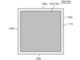
図1は、実施形態1に係るセラミックス回路基板100の上面図である。図2は、図1に示したセラミックス回路基板100の下面図である。図3は、図1のA-A´断面図である。
図4は、実施形態2に係る放熱部材200の上面図である。図5は、図4のB-B´断面図である。
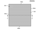
図6は、実施形態3に係るアルミニウム-ダイヤモンド系複合体300の上面図である。図7は、図6のC-C´断面図である。
以下、参考形態の例を付記する。
1. 金属層と、
前記金属層の表面に形成されたマーカ部と、
を備えるセラミックス回路基板。
2. 1.に記載のセラミックス回路基板において、
前記マーカ部は、前記金属層の前記表面にレーザで形成された凹部である、セラミックス回路基板。
3. 1.に記載のセラミックス回路基板において、
前記マーカ部は、塗料によって形成されている、セラミックス回路基板。
4. 1.から3.までのいずれか一つに記載のセラミックス回路基板において、
前記マーカ部は、一次元コード及び二次元コードのうちの少なくとも一方である、セラミックス回路基板。
5. 1.から4.までのいずれか一つに記載のセラミックス回路基板において、
前記マーカ部は、前記セラミックス回路基板の製造条件を含む情報を示す、セラミックス回路基板。
6. 放熱部材であって、
放熱フィンが取り付けられる第1面と、
前記第1面の反対側にあって、マーカ部が形成された第2面と、
を備える放熱部材。
7. 6.に記載の放熱部材において、
前記マーカ部は、前記放熱部材の前記第2面にレーザで形成された凹部である、放熱部材。
8. 6.に記載の放熱部材において、
前記マーカ部は、塗料によって形成されている、放熱部材。
9. 6.から8.までのいずれか一つに記載の放熱部材において、
前記マーカ部は、一次元コード及び二次元コードのうちの少なくとも一方である、放熱部材。
10. 6.から9.までのいずれか一つに記載の放熱部材において、
前記マーカ部は、前記放熱部材の反りの向きを含む情報を示す、放熱部材。
11. 6.から10.までのいずれか一つに記載の放熱部材において、
前記マーカ部は、前記放熱部材の製造条件を含む情報を示す、放熱部材。
12. ダイヤモンド粒子とアルミニウムを主成分とする金属とを含む平板状のアルミニウム-ダイヤモンド系複合体であって、
前記アルミニウム-ダイヤモンド系複合体は複合化部及び前記複合化部の両面に設けられた表面層からなり、
前記表面層がアルミニウムを主成分とする金属を含む材料からなり、
前記表面層の表面に形成されたマーカ部を備えるアルミニウム-ダイヤモンド系複合体。
13. 12.に記載のアルミニウム-ダイヤモンド系複合体において、
前記マーカ部は、前記表面にレーザで形成された凹部である、アルミニウム-ダイヤモンド系複合体。
14. 12.に記載のアルミニウム-ダイヤモンド系複合体において、
前記マーカ部は、塗料によって形成されている、アルミニウム-ダイヤモンド系複合体。
15. 12.から14.までのいずれか一つに記載のアルミニウム-ダイヤモンド系複合体において、
前記マーカ部は、一次元コード及び二次元コードのうちの少なくとも一方である、アルミニウム-ダイヤモンド系複合体。
16. 12.から15.までのいずれか一つに記載のアルミニウム-ダイヤモンド系複合体において、
前記マーカ部は、前記アルミニウム-ダイヤモンド系複合体の製造条件を含む情報を示す、アルミニウム-ダイヤモンド系複合体。
102 第1面
104 第2面
106a 第1側面
106b 第2側面
106c 第3側面
106d 第4側面
110 セラミックス基材
120 金属層
122 第1金属層
124 第2金属層
150 マーカ部
200 マーカ
200 放熱部材
202 凹部
202 第1面
204 第2面
206a 第1側面
206b 第2側面
206c 第3側面
206d 第4側面
210 放熱フィン
212 グリス
250 マーカ部
302 第1面
304 第2面
306a 第1側面
306b 第2側面
306c 第3側面
306d 第4側面
310 複合化部
320 表面層
322 第1表面層
324 第2表面層
350 マーカ部
Claims (10)
- 金属層と、
前記金属層の表面に形成されたマーカ部と、
を備え、
前記マーカ部は、前記金属層の前記表面にレーザで形成された凹部であり、
前記凹部は、10μm以上200μm以下の幅及び10μm以上200μm以下の深さを有する、セラミックス回路基板。 - 請求項1に記載のセラミックス回路基板において、
前記マーカ部は、一次元コード及び二次元コードのうちの少なくとも一方である、セラミックス回路基板。 - 請求項1又は2に記載のセラミックス回路基板において、
前記マーカ部は、前記セラミックス回路基板の製造条件を含む情報を示す、セラミックス回路基板。 - 放熱部材であって、
放熱フィンが取り付けられる第1面と、
前記第1面の反対側にあって、マーカ部が形成された第2面と、
を備え、
前記マーカ部は、前記放熱部材の前記第2面にレーザで形成された凹部であり、
前記凹部は、10μm以上200μm以下の幅及び10μm以上200μm以下の深さを有する、放熱部材。 - 請求項4に記載の放熱部材において、
前記マーカ部は、一次元コード及び二次元コードのうちの少なくとも一方である、放熱部材。 - 請求項4又は5に記載の放熱部材において、
前記マーカ部は、前記放熱部材の反りの向きを含む情報を示す、放熱部材。 - 請求項4から6までのいずれか一項に記載の放熱部材において、
前記マーカ部は、前記放熱部材の製造条件を含む情報を示す、放熱部材。 - ダイヤモンド粒子とアルミニウムを主成分とする金属とを含む平板状のアルミニウム-ダイヤモンド系複合体であって、
前記アルミニウム-ダイヤモンド系複合体は複合化部及び前記複合化部の両面に設けられた表面層からなり、
前記表面層がアルミニウムを主成分とする金属を含む材料からなり、
前記表面層の表面に形成されたマーカ部を備え、
前記マーカ部は、前記表面にレーザで形成された凹部であり、
前記凹部は、10μm以上200μm以下の幅及び10μm以上200μm以下の深さを有する、アルミニウム-ダイヤモンド系複合体。 - 請求項8に記載のアルミニウム-ダイヤモンド系複合体において、
前記マーカ部は、一次元コード及び二次元コードのうちの少なくとも一方である、アルミニウム-ダイヤモンド系複合体。 - 請求項8又は9に記載のアルミニウム-ダイヤモンド系複合体において、
前記マーカ部は、前記アルミニウム-ダイヤモンド系複合体の製造条件を含む情報を示す、アルミニウム-ダイヤモンド系複合体。
Applications Claiming Priority (3)
| Application Number | Priority Date | Filing Date | Title |
|---|---|---|---|
| JP2020055457 | 2020-03-26 | ||
| JP2020055457 | 2020-03-26 | ||
| PCT/JP2021/012500 WO2021193810A1 (ja) | 2020-03-26 | 2021-03-25 | セラミックス回路基板、放熱部材及びアルミニウム-ダイヤモンド系複合体 |
Publications (3)
| Publication Number | Publication Date |
|---|---|
| JPWO2021193810A1 JPWO2021193810A1 (ja) | 2021-09-30 |
| JPWO2021193810A5 JPWO2021193810A5 (ja) | 2022-12-01 |
| JP7587570B2 true JP7587570B2 (ja) | 2024-11-20 |
Family
ID=77891886
Family Applications (1)
| Application Number | Title | Priority Date | Filing Date |
|---|---|---|---|
| JP2022510653A Active JP7587570B2 (ja) | 2020-03-26 | 2021-03-25 | セラミックス回路基板、放熱部材及びアルミニウム-ダイヤモンド系複合体 |
Country Status (6)
| Country | Link |
|---|---|
| US (1) | US11983586B2 (ja) |
| EP (1) | EP4131361A4 (ja) |
| JP (1) | JP7587570B2 (ja) |
| KR (1) | KR20220159950A (ja) |
| CN (1) | CN115053638A (ja) |
| WO (1) | WO2021193810A1 (ja) |
Families Citing this family (2)
| Publication number | Priority date | Publication date | Assignee | Title |
|---|---|---|---|---|
| WO2022109552A1 (en) * | 2020-11-18 | 2022-05-27 | Sharfi Benjamin K | Diamond-based thermal cooling devices methods and materials |
| DE102023119620A1 (de) * | 2023-07-25 | 2025-01-30 | Rogers Germany Gmbh | Verfahren zur Herstellung und/oder Handhabung eines Metall-Keramik-Substrats, ein Metall-Keramik-Substrat, eine Anlage zur Herstellung von Metall-Keramik-Substraten und Datenbank für Metall-Keramik-Substrate |
Citations (6)
| Publication number | Priority date | Publication date | Assignee | Title |
|---|---|---|---|---|
| JP2008518384A (ja) | 2004-11-01 | 2008-05-29 | 松下電器産業株式会社 | 発光モジュール、照明装置及び表示装置 |
| JP2009130156A (ja) | 2007-11-26 | 2009-06-11 | Seiko Epson Corp | セラミック多層基板及びセラミック多層基板の製造方法 |
| WO2010007922A1 (ja) | 2008-07-17 | 2010-01-21 | 電気化学工業株式会社 | アルミニウム-ダイヤモンド系複合体及びその製造方法 |
| US20200009891A1 (en) | 2018-07-03 | 2020-01-09 | Apple Inc. | Controlled ablation and surface modification for marking an electronic device |
| CN110690176A (zh) | 2019-10-14 | 2020-01-14 | 长江存储科技有限责任公司 | 目标晶粒的区分方法及封装芯片的失效分析方法 |
| WO2020025497A1 (fr) | 2018-08-01 | 2020-02-06 | Saint-Gobain Centre De Recherches Et D'etudes Europeen | Procede de marquage d'une piece ceramique refractaire |
Family Cites Families (18)
| Publication number | Priority date | Publication date | Assignee | Title |
|---|---|---|---|---|
| JPS62158034A (ja) | 1986-01-07 | 1987-07-14 | 川崎製鉄株式会社 | 金属箔複合体 |
| JPH06333073A (ja) * | 1993-05-18 | 1994-12-02 | Nichion Irika Kikai Seisakusho:Kk | コードマーク読み取り装置 |
| JP3361504B2 (ja) | 2000-05-24 | 2003-01-07 | 株式会社イメ−ジパ−トナ− | カード支払自動決済システム |
| JP2002346633A (ja) * | 2001-05-29 | 2002-12-03 | Daido Steel Co Ltd | レーザーマーキング方法 |
| JP2005520334A (ja) | 2002-03-13 | 2005-07-07 | スチュルス−ハーダー,ジャーヘン | 金属−セラミック基板、好ましくは銅−セラミック基板を製造するプロセス |
| JP2006253183A (ja) | 2005-03-08 | 2006-09-21 | Hitachi Ltd | 半導体パワーモジュール |
| WO2012176473A1 (ja) * | 2011-06-22 | 2012-12-27 | パナソニック株式会社 | ドットマーキングを有する半導体基板、およびその製造方法 |
| JP5523415B2 (ja) | 2011-09-06 | 2014-06-18 | 三菱電機株式会社 | 冷却機器及び静電霧化装置及び空気調和機 |
| JP2013247256A (ja) * | 2012-05-28 | 2013-12-09 | Hitachi Ltd | 半導体装置およびその製造方法 |
| JP6091035B2 (ja) * | 2014-10-29 | 2017-03-15 | 新電元工業株式会社 | 放熱構造 |
| US9799584B2 (en) | 2015-11-16 | 2017-10-24 | Intel Corporation | Heat spreaders with integrated preforms |
| HUE064697T2 (hu) * | 2015-12-22 | 2024-04-28 | Heraeus Electronics Gmbh & Co Kg | Eljárás fém-kerámia hordozók egyedi kódolására |
| WO2018123380A1 (ja) * | 2016-12-28 | 2018-07-05 | デンカ株式会社 | 半導体素子用放熱部品 |
| WO2018146933A1 (ja) | 2017-02-13 | 2018-08-16 | 富士電機株式会社 | 半導体装置及び半導体装置の製造方法 |
| EP3361504A1 (en) | 2017-02-14 | 2018-08-15 | Infineon Technologies AG | Power electronic substrate with marker, manufacturing of a power electronic substrate and detection of a marker |
| JP6799479B2 (ja) * | 2017-03-03 | 2020-12-16 | Dowaメタルテック株式会社 | 金属−セラミックス回路基板の製造方法 |
| JP6760518B2 (ja) | 2017-11-17 | 2020-09-23 | 三菱電機株式会社 | 半導体モジュール |
| JP7129304B2 (ja) | 2018-10-03 | 2022-09-01 | Toyo Tire株式会社 | タイヤ |
-
2021
- 2021-03-25 JP JP2022510653A patent/JP7587570B2/ja active Active
- 2021-03-25 CN CN202180010953.4A patent/CN115053638A/zh active Pending
- 2021-03-25 EP EP21776350.7A patent/EP4131361A4/en not_active Ceased
- 2021-03-25 KR KR1020227023670A patent/KR20220159950A/ko not_active Ceased
- 2021-03-25 US US17/791,971 patent/US11983586B2/en active Active
- 2021-03-25 WO PCT/JP2021/012500 patent/WO2021193810A1/ja not_active Ceased
Patent Citations (6)
| Publication number | Priority date | Publication date | Assignee | Title |
|---|---|---|---|---|
| JP2008518384A (ja) | 2004-11-01 | 2008-05-29 | 松下電器産業株式会社 | 発光モジュール、照明装置及び表示装置 |
| JP2009130156A (ja) | 2007-11-26 | 2009-06-11 | Seiko Epson Corp | セラミック多層基板及びセラミック多層基板の製造方法 |
| WO2010007922A1 (ja) | 2008-07-17 | 2010-01-21 | 電気化学工業株式会社 | アルミニウム-ダイヤモンド系複合体及びその製造方法 |
| US20200009891A1 (en) | 2018-07-03 | 2020-01-09 | Apple Inc. | Controlled ablation and surface modification for marking an electronic device |
| WO2020025497A1 (fr) | 2018-08-01 | 2020-02-06 | Saint-Gobain Centre De Recherches Et D'etudes Europeen | Procede de marquage d'une piece ceramique refractaire |
| CN110690176A (zh) | 2019-10-14 | 2020-01-14 | 长江存储科技有限责任公司 | 目标晶粒的区分方法及封装芯片的失效分析方法 |
Also Published As
| Publication number | Publication date |
|---|---|
| JPWO2021193810A1 (ja) | 2021-09-30 |
| US20230042932A1 (en) | 2023-02-09 |
| CN115053638A (zh) | 2022-09-13 |
| US11983586B2 (en) | 2024-05-14 |
| KR20220159950A (ko) | 2022-12-05 |
| EP4131361A1 (en) | 2023-02-08 |
| WO2021193810A1 (ja) | 2021-09-30 |
| EP4131361A4 (en) | 2024-02-14 |
Similar Documents
| Publication | Publication Date | Title |
|---|---|---|
| US6554060B2 (en) | Heat sink with fins | |
| US7038313B2 (en) | Semiconductor device and method of manufacturing the same | |
| JP7587570B2 (ja) | セラミックス回路基板、放熱部材及びアルミニウム-ダイヤモンド系複合体 | |
| JP2013522872A (ja) | 金属接合セラミック基板 | |
| JP2005011922A (ja) | ヒートシンクを備えた両面銅貼り基板、およびこれを用いた半導体装置 | |
| JP4806803B2 (ja) | 金属−セラミックス接合基板およびその製造方法 | |
| JP2011222706A (ja) | 半導体パッケージ | |
| JP2010062203A (ja) | 放熱基板ユニット | |
| JP2004153075A (ja) | パワーモジュール用基板及びパワーモジュール | |
| JP4416362B2 (ja) | 半導体素子用放熱性部品及び半導体装置 | |
| JP6799392B2 (ja) | 金属−セラミックス接合基板およびその製造方法 | |
| JP2006269966A (ja) | 配線基板およびその製造方法 | |
| JPH06181396A (ja) | 回路基板のヒートパイプ式冷却装置 | |
| JP2003318579A (ja) | 放熱板付きfetの放熱方法 | |
| JP5299304B2 (ja) | パワーモジュール用基板の製造方法およびパワーモジュール用基板の製造中間体 | |
| KR102678847B1 (ko) | 방열 및 휨 방지를 위한 코팅층을 가진 반도체 패키지 | |
| JP2753140B2 (ja) | 半導体用回路基板 | |
| JP7662505B2 (ja) | 放熱基板 | |
| JP6320347B2 (ja) | 半導体装置 | |
| JP3901109B2 (ja) | 放熱体の製造方法及び放熱体並びにこの放熱体を用いたパワーモジュール用基板及びパワーモジュール | |
| JP2004140159A (ja) | 放熱体 | |
| KR20250045920A (ko) | Led 방열 프레임 구조 | |
| JP3873870B2 (ja) | 放熱体 | |
| KR20250103430A (ko) | 히트싱크 | |
| JP3408606B2 (ja) | 金属ベース多層回路基板の製造方法 |
Legal Events
| Date | Code | Title | Description |
|---|---|---|---|
| A521 | Request for written amendment filed |
Free format text: JAPANESE INTERMEDIATE CODE: A523 Effective date: 20220620 |
|
| A621 | Written request for application examination |
Free format text: JAPANESE INTERMEDIATE CODE: A621 Effective date: 20230524 |
|
| A131 | Notification of reasons for refusal |
Free format text: JAPANESE INTERMEDIATE CODE: A131 Effective date: 20240423 |
|
| A521 | Request for written amendment filed |
Free format text: JAPANESE INTERMEDIATE CODE: A523 Effective date: 20240509 |
|
| A02 | Decision of refusal |
Free format text: JAPANESE INTERMEDIATE CODE: A02 Effective date: 20240702 |
|
| A521 | Request for written amendment filed |
Free format text: JAPANESE INTERMEDIATE CODE: A523 Effective date: 20240805 |
|
| A911 | Transfer to examiner for re-examination before appeal (zenchi) |
Free format text: JAPANESE INTERMEDIATE CODE: A911 Effective date: 20240813 |
|
| TRDD | Decision of grant or rejection written | ||
| A01 | Written decision to grant a patent or to grant a registration (utility model) |
Free format text: JAPANESE INTERMEDIATE CODE: A01 Effective date: 20241022 |
|
| A61 | First payment of annual fees (during grant procedure) |
Free format text: JAPANESE INTERMEDIATE CODE: A61 Effective date: 20241108 |
|
| R150 | Certificate of patent or registration of utility model |
Ref document number: 7587570 Country of ref document: JP Free format text: JAPANESE INTERMEDIATE CODE: R150 |