JP7616771B2 - アモルファスシリコン膜の結晶化方法 - Google Patents
アモルファスシリコン膜の結晶化方法 Download PDFInfo
- Publication number
- JP7616771B2 JP7616771B2 JP2021064988A JP2021064988A JP7616771B2 JP 7616771 B2 JP7616771 B2 JP 7616771B2 JP 2021064988 A JP2021064988 A JP 2021064988A JP 2021064988 A JP2021064988 A JP 2021064988A JP 7616771 B2 JP7616771 B2 JP 7616771B2
- Authority
- JP
- Japan
- Prior art keywords
- amorphous silicon
- silicon film
- temperature
- gas
- forming
- Prior art date
- Legal status (The legal status is an assumption and is not a legal conclusion. Google has not performed a legal analysis and makes no representation as to the accuracy of the status listed.)
- Active
Links
Images




Classifications
-
- H—ELECTRICITY
- H10—SEMICONDUCTOR DEVICES; ELECTRIC SOLID-STATE DEVICES NOT OTHERWISE PROVIDED FOR
- H10P—GENERIC PROCESSES OR APPARATUS FOR THE MANUFACTURE OR TREATMENT OF DEVICES COVERED BY CLASS H10
- H10P14/00—Formation of materials, e.g. in the shape of layers or pillars
- H10P14/20—Formation of materials, e.g. in the shape of layers or pillars of semiconductor materials
- H10P14/38—Formation of materials, e.g. in the shape of layers or pillars of semiconductor materials characterised by treatments done after the formation of the materials
- H10P14/3802—Crystallisation or recrystallisation of non-monocrystalline semiconductor materials, e.g. regrowth
-
- C—CHEMISTRY; METALLURGY
- C23—COATING METALLIC MATERIAL; COATING MATERIAL WITH METALLIC MATERIAL; CHEMICAL SURFACE TREATMENT; DIFFUSION TREATMENT OF METALLIC MATERIAL; COATING BY VACUUM EVAPORATION, BY SPUTTERING, BY ION IMPLANTATION OR BY CHEMICAL VAPOUR DEPOSITION, IN GENERAL; INHIBITING CORROSION OF METALLIC MATERIAL OR INCRUSTATION IN GENERAL
- C23C—COATING METALLIC MATERIAL; COATING MATERIAL WITH METALLIC MATERIAL; SURFACE TREATMENT OF METALLIC MATERIAL BY DIFFUSION INTO THE SURFACE, BY CHEMICAL CONVERSION OR SUBSTITUTION; COATING BY VACUUM EVAPORATION, BY SPUTTERING, BY ION IMPLANTATION OR BY CHEMICAL VAPOUR DEPOSITION, IN GENERAL
- C23C16/00—Chemical coating by decomposition of gaseous compounds, without leaving reaction products of surface material in the coating, i.e. chemical vapour deposition [CVD] processes
- C23C16/02—Pretreatment of the material to be coated
- C23C16/0272—Deposition of sub-layers, e.g. to promote the adhesion of the main coating
-
- C—CHEMISTRY; METALLURGY
- C23—COATING METALLIC MATERIAL; COATING MATERIAL WITH METALLIC MATERIAL; CHEMICAL SURFACE TREATMENT; DIFFUSION TREATMENT OF METALLIC MATERIAL; COATING BY VACUUM EVAPORATION, BY SPUTTERING, BY ION IMPLANTATION OR BY CHEMICAL VAPOUR DEPOSITION, IN GENERAL; INHIBITING CORROSION OF METALLIC MATERIAL OR INCRUSTATION IN GENERAL
- C23C—COATING METALLIC MATERIAL; COATING MATERIAL WITH METALLIC MATERIAL; SURFACE TREATMENT OF METALLIC MATERIAL BY DIFFUSION INTO THE SURFACE, BY CHEMICAL CONVERSION OR SUBSTITUTION; COATING BY VACUUM EVAPORATION, BY SPUTTERING, BY ION IMPLANTATION OR BY CHEMICAL VAPOUR DEPOSITION, IN GENERAL
- C23C16/00—Chemical coating by decomposition of gaseous compounds, without leaving reaction products of surface material in the coating, i.e. chemical vapour deposition [CVD] processes
- C23C16/22—Chemical coating by decomposition of gaseous compounds, without leaving reaction products of surface material in the coating, i.e. chemical vapour deposition [CVD] processes characterised by the deposition of inorganic material, other than metallic material
- C23C16/24—Deposition of silicon only
-
- C—CHEMISTRY; METALLURGY
- C23—COATING METALLIC MATERIAL; COATING MATERIAL WITH METALLIC MATERIAL; CHEMICAL SURFACE TREATMENT; DIFFUSION TREATMENT OF METALLIC MATERIAL; COATING BY VACUUM EVAPORATION, BY SPUTTERING, BY ION IMPLANTATION OR BY CHEMICAL VAPOUR DEPOSITION, IN GENERAL; INHIBITING CORROSION OF METALLIC MATERIAL OR INCRUSTATION IN GENERAL
- C23C—COATING METALLIC MATERIAL; COATING MATERIAL WITH METALLIC MATERIAL; SURFACE TREATMENT OF METALLIC MATERIAL BY DIFFUSION INTO THE SURFACE, BY CHEMICAL CONVERSION OR SUBSTITUTION; COATING BY VACUUM EVAPORATION, BY SPUTTERING, BY ION IMPLANTATION OR BY CHEMICAL VAPOUR DEPOSITION, IN GENERAL
- C23C16/00—Chemical coating by decomposition of gaseous compounds, without leaving reaction products of surface material in the coating, i.e. chemical vapour deposition [CVD] processes
- C23C16/44—Chemical coating by decomposition of gaseous compounds, without leaving reaction products of surface material in the coating, i.e. chemical vapour deposition [CVD] processes characterised by the method of coating
- C23C16/52—Controlling or regulating the coating process
-
- C—CHEMISTRY; METALLURGY
- C23—COATING METALLIC MATERIAL; COATING MATERIAL WITH METALLIC MATERIAL; CHEMICAL SURFACE TREATMENT; DIFFUSION TREATMENT OF METALLIC MATERIAL; COATING BY VACUUM EVAPORATION, BY SPUTTERING, BY ION IMPLANTATION OR BY CHEMICAL VAPOUR DEPOSITION, IN GENERAL; INHIBITING CORROSION OF METALLIC MATERIAL OR INCRUSTATION IN GENERAL
- C23C—COATING METALLIC MATERIAL; COATING MATERIAL WITH METALLIC MATERIAL; SURFACE TREATMENT OF METALLIC MATERIAL BY DIFFUSION INTO THE SURFACE, BY CHEMICAL CONVERSION OR SUBSTITUTION; COATING BY VACUUM EVAPORATION, BY SPUTTERING, BY ION IMPLANTATION OR BY CHEMICAL VAPOUR DEPOSITION, IN GENERAL
- C23C16/00—Chemical coating by decomposition of gaseous compounds, without leaving reaction products of surface material in the coating, i.e. chemical vapour deposition [CVD] processes
- C23C16/56—After-treatment
-
- H—ELECTRICITY
- H10—SEMICONDUCTOR DEVICES; ELECTRIC SOLID-STATE DEVICES NOT OTHERWISE PROVIDED FOR
- H10P—GENERIC PROCESSES OR APPARATUS FOR THE MANUFACTURE OR TREATMENT OF DEVICES COVERED BY CLASS H10
- H10P14/00—Formation of materials, e.g. in the shape of layers or pillars
- H10P14/20—Formation of materials, e.g. in the shape of layers or pillars of semiconductor materials
- H10P14/24—Formation of materials, e.g. in the shape of layers or pillars of semiconductor materials using chemical vapour deposition [CVD]
-
- H—ELECTRICITY
- H10—SEMICONDUCTOR DEVICES; ELECTRIC SOLID-STATE DEVICES NOT OTHERWISE PROVIDED FOR
- H10P—GENERIC PROCESSES OR APPARATUS FOR THE MANUFACTURE OR TREATMENT OF DEVICES COVERED BY CLASS H10
- H10P14/00—Formation of materials, e.g. in the shape of layers or pillars
- H10P14/20—Formation of materials, e.g. in the shape of layers or pillars of semiconductor materials
- H10P14/27—Formation of materials, e.g. in the shape of layers or pillars of semiconductor materials using selective deposition, e.g. simultaneous growth of monocrystalline and non-monocrystalline semiconductor materials
- H10P14/271—Formation of materials, e.g. in the shape of layers or pillars of semiconductor materials using selective deposition, e.g. simultaneous growth of monocrystalline and non-monocrystalline semiconductor materials characterised by the preparation of substrate for selective deposition
- H10P14/274—Formation of materials, e.g. in the shape of layers or pillars of semiconductor materials using selective deposition, e.g. simultaneous growth of monocrystalline and non-monocrystalline semiconductor materials characterised by the preparation of substrate for selective deposition using seed materials
-
- H—ELECTRICITY
- H10—SEMICONDUCTOR DEVICES; ELECTRIC SOLID-STATE DEVICES NOT OTHERWISE PROVIDED FOR
- H10P—GENERIC PROCESSES OR APPARATUS FOR THE MANUFACTURE OR TREATMENT OF DEVICES COVERED BY CLASS H10
- H10P14/00—Formation of materials, e.g. in the shape of layers or pillars
- H10P14/20—Formation of materials, e.g. in the shape of layers or pillars of semiconductor materials
- H10P14/32—Formation of materials, e.g. in the shape of layers or pillars of semiconductor materials characterised by intermediate layers between substrates and deposited layers
- H10P14/3202—Materials thereof
- H10P14/3204—Materials thereof being Group IVA semiconducting materials
- H10P14/3211—Silicon, silicon germanium or germanium
-
- H—ELECTRICITY
- H10—SEMICONDUCTOR DEVICES; ELECTRIC SOLID-STATE DEVICES NOT OTHERWISE PROVIDED FOR
- H10P—GENERIC PROCESSES OR APPARATUS FOR THE MANUFACTURE OR TREATMENT OF DEVICES COVERED BY CLASS H10
- H10P14/00—Formation of materials, e.g. in the shape of layers or pillars
- H10P14/20—Formation of materials, e.g. in the shape of layers or pillars of semiconductor materials
- H10P14/32—Formation of materials, e.g. in the shape of layers or pillars of semiconductor materials characterised by intermediate layers between substrates and deposited layers
- H10P14/3202—Materials thereof
- H10P14/3238—Materials thereof being insulating materials
-
- H—ELECTRICITY
- H10—SEMICONDUCTOR DEVICES; ELECTRIC SOLID-STATE DEVICES NOT OTHERWISE PROVIDED FOR
- H10P—GENERIC PROCESSES OR APPARATUS FOR THE MANUFACTURE OR TREATMENT OF DEVICES COVERED BY CLASS H10
- H10P14/00—Formation of materials, e.g. in the shape of layers or pillars
- H10P14/20—Formation of materials, e.g. in the shape of layers or pillars of semiconductor materials
- H10P14/32—Formation of materials, e.g. in the shape of layers or pillars of semiconductor materials characterised by intermediate layers between substrates and deposited layers
- H10P14/3242—Structure
- H10P14/3244—Layer structure
- H10P14/3248—Layer structure consisting of two layers
-
- H—ELECTRICITY
- H10—SEMICONDUCTOR DEVICES; ELECTRIC SOLID-STATE DEVICES NOT OTHERWISE PROVIDED FOR
- H10P—GENERIC PROCESSES OR APPARATUS FOR THE MANUFACTURE OR TREATMENT OF DEVICES COVERED BY CLASS H10
- H10P14/00—Formation of materials, e.g. in the shape of layers or pillars
- H10P14/20—Formation of materials, e.g. in the shape of layers or pillars of semiconductor materials
- H10P14/34—Deposited materials, e.g. layers
- H10P14/3402—Deposited materials, e.g. layers characterised by the chemical composition
- H10P14/3404—Deposited materials, e.g. layers characterised by the chemical composition being Group IVA materials
- H10P14/3411—Silicon, silicon germanium or germanium
-
- H—ELECTRICITY
- H10—SEMICONDUCTOR DEVICES; ELECTRIC SOLID-STATE DEVICES NOT OTHERWISE PROVIDED FOR
- H10P—GENERIC PROCESSES OR APPARATUS FOR THE MANUFACTURE OR TREATMENT OF DEVICES COVERED BY CLASS H10
- H10P14/00—Formation of materials, e.g. in the shape of layers or pillars
- H10P14/20—Formation of materials, e.g. in the shape of layers or pillars of semiconductor materials
- H10P14/34—Deposited materials, e.g. layers
- H10P14/3451—Structure
- H10P14/3452—Microstructure
- H10P14/3454—Amorphous
Landscapes
- Chemical & Material Sciences (AREA)
- General Chemical & Material Sciences (AREA)
- Chemical Kinetics & Catalysis (AREA)
- Engineering & Computer Science (AREA)
- Materials Engineering (AREA)
- Mechanical Engineering (AREA)
- Metallurgy (AREA)
- Organic Chemistry (AREA)
- Inorganic Chemistry (AREA)
- Recrystallisation Techniques (AREA)
- Crystallography & Structural Chemistry (AREA)
- Chemical Vapour Deposition (AREA)
Description
前記アモルファスシリコン膜を前記第1の温度よりも高い第2の温度で加熱して前記アモルファスシリコン膜の表層のシリコンを凝集させ、前記表層に結晶核を形成する工程と、を有し、前記結晶核を形成する工程は、前記アモルファスシリコン膜の表層から真空排気で水素を脱離させ、水素濃度の低い膜を形成することを含む。
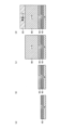
図6は、本開示の実施形態に係るアモルファスシリコン膜の結晶化方法を本実施形態に係る成膜装置で実施した実施例を示した図である。
19 ヒーター
21、31 ガス導入管
23A~23C、32 ガス供給源
24A~24C、33 ガス供給機構
27 バルブ
30 制御部
40 シリコン酸化膜
50 シード層
60、62、65 アモルファスシリコン膜
61 結晶核
W ウエハ
Claims (6)
- 基板上に形成されたシード層上にアモルファスシリコン膜を第1の温度で加熱しながら形成する工程と、
前記アモルファスシリコン膜を前記第1の温度よりも高い第2の温度で加熱して前記アモルファスシリコン膜の表層のシリコンを凝集させ、前記表層に結晶核を形成する工程と、を有し、
前記結晶核を形成する工程は、前記アモルファスシリコン膜の表層から真空排気で水素を脱離させ、水素濃度の低い膜を形成することを含む、
アモルファスシリコン膜の結晶化方法。 - 前記第1の温度は440℃以上530℃未満の範囲内であり、
前記第2の温度は550℃以上600℃未満の範囲内である請求項1に記載のアモルファスシリコン膜の結晶化方法。 - 前記結晶核を形成する工程は、560℃以上580℃以下の温度で行われる請求項2に記載のアモルファスシリコン膜の結晶化方法。
- 前記アモルファスシリコン膜を形成する工程の前に、前記基板上にシリコンからなる前記シード層を形成する工程を更に有する請求項1乃至3のいずれか一項に記載のアモルファスシリコン膜の結晶化方法。
- 前記結晶核を形成する工程の後に、前記第2の温度よりも高い第3の温度で前記アモルファスシリコン膜をアニールする工程を更に有する請求項1乃至4のいずれか一項に記載のアモルファスシリコン膜の結晶化方法。
- 前記第3の温度は、650℃以上750℃以下の温度である請求項5に記載のアモルファスシリコン膜の結晶化方法。
Priority Applications (3)
| Application Number | Priority Date | Filing Date | Title |
|---|---|---|---|
| JP2021064988A JP7616771B2 (ja) | 2021-04-06 | 2021-04-06 | アモルファスシリコン膜の結晶化方法 |
| US17/655,247 US12112947B2 (en) | 2021-04-06 | 2022-03-17 | Method of crystallizing amorphous silicon film and deposition apparatus |
| KR1020220037016A KR102935311B1 (ko) | 2021-04-06 | 2022-03-25 | 아몰퍼스 실리콘막의 결정화 방법 및 성막 장치 |
Applications Claiming Priority (1)
| Application Number | Priority Date | Filing Date | Title |
|---|---|---|---|
| JP2021064988A JP7616771B2 (ja) | 2021-04-06 | 2021-04-06 | アモルファスシリコン膜の結晶化方法 |
Publications (2)
| Publication Number | Publication Date |
|---|---|
| JP2022160318A JP2022160318A (ja) | 2022-10-19 |
| JP7616771B2 true JP7616771B2 (ja) | 2025-01-17 |
Family
ID=83448357
Family Applications (1)
| Application Number | Title | Priority Date | Filing Date |
|---|---|---|---|
| JP2021064988A Active JP7616771B2 (ja) | 2021-04-06 | 2021-04-06 | アモルファスシリコン膜の結晶化方法 |
Country Status (3)
| Country | Link |
|---|---|
| US (1) | US12112947B2 (ja) |
| JP (1) | JP7616771B2 (ja) |
| KR (1) | KR102935311B1 (ja) |
Citations (4)
| Publication number | Priority date | Publication date | Assignee | Title |
|---|---|---|---|---|
| US20070105305A1 (en) | 2003-03-17 | 2007-05-10 | Shuo Gu | Method to form large grain size polysilicon films by nuclei-induced solid phase crystallization |
| JP2015115435A (ja) | 2013-12-11 | 2015-06-22 | 東京エレクトロン株式会社 | アモルファスシリコンの結晶化方法、結晶化シリコン膜の成膜方法、半導体装置の製造方法および成膜装置 |
| JP2019121620A (ja) | 2017-12-28 | 2019-07-22 | 株式会社Kokusai Electric | 半導体装置の製造方法、基板処理装置、およびプログラム |
| JP2020087993A (ja) | 2018-11-16 | 2020-06-04 | 東京エレクトロン株式会社 | ポリシリコン膜の形成方法及び成膜装置 |
Family Cites Families (10)
| Publication number | Priority date | Publication date | Assignee | Title |
|---|---|---|---|---|
| JPH07142405A (ja) * | 1993-11-19 | 1995-06-02 | Sanyo Electric Co Ltd | 多結晶半導体膜およびその成膜方法 |
| JPH09232529A (ja) * | 1996-02-21 | 1997-09-05 | Mitsubishi Electric Corp | 半導体記憶装置およびその製造方法 |
| JP2795316B2 (ja) * | 1996-05-21 | 1998-09-10 | 日本電気株式会社 | 半導体装置の製造方法 |
| JP3727449B2 (ja) * | 1997-09-30 | 2005-12-14 | シャープ株式会社 | 半導体ナノ結晶の製造方法 |
| JP4376979B2 (ja) * | 1998-01-12 | 2009-12-02 | 株式会社半導体エネルギー研究所 | 半導体装置の作製方法 |
| JP4876306B2 (ja) * | 2000-10-19 | 2012-02-15 | ソニー株式会社 | 半導体装置の製造方法 |
| JP2006237270A (ja) * | 2005-02-24 | 2006-09-07 | Sony Corp | 薄膜半導体装置及びその製造方法と表示装置 |
| JP2011187609A (ja) * | 2010-03-08 | 2011-09-22 | Seiko Epson Corp | 半導体装置の製造方法、電気光学装置、電子機器 |
| JP2011216759A (ja) * | 2010-04-01 | 2011-10-27 | Seiko Epson Corp | 結晶化シリコン層の製造方法、半導体装置の製造方法、電気光学装置の製造方法、半導体装置、電気光学装置および投射型表示装置 |
| JP6082712B2 (ja) | 2013-07-31 | 2017-02-15 | 東京エレクトロン株式会社 | シリコン膜の成膜方法および薄膜の成膜方法 |
-
2021
- 2021-04-06 JP JP2021064988A patent/JP7616771B2/ja active Active
-
2022
- 2022-03-17 US US17/655,247 patent/US12112947B2/en active Active
- 2022-03-25 KR KR1020220037016A patent/KR102935311B1/ko active Active
Patent Citations (4)
| Publication number | Priority date | Publication date | Assignee | Title |
|---|---|---|---|---|
| US20070105305A1 (en) | 2003-03-17 | 2007-05-10 | Shuo Gu | Method to form large grain size polysilicon films by nuclei-induced solid phase crystallization |
| JP2015115435A (ja) | 2013-12-11 | 2015-06-22 | 東京エレクトロン株式会社 | アモルファスシリコンの結晶化方法、結晶化シリコン膜の成膜方法、半導体装置の製造方法および成膜装置 |
| JP2019121620A (ja) | 2017-12-28 | 2019-07-22 | 株式会社Kokusai Electric | 半導体装置の製造方法、基板処理装置、およびプログラム |
| JP2020087993A (ja) | 2018-11-16 | 2020-06-04 | 東京エレクトロン株式会社 | ポリシリコン膜の形成方法及び成膜装置 |
Also Published As
| Publication number | Publication date |
|---|---|
| JP2022160318A (ja) | 2022-10-19 |
| US20220319846A1 (en) | 2022-10-06 |
| KR20220138805A (ko) | 2022-10-13 |
| KR102935311B1 (ko) | 2026-03-09 |
| US12112947B2 (en) | 2024-10-08 |
Similar Documents
| Publication | Publication Date | Title |
|---|---|---|
| JP5393895B2 (ja) | 半導体装置の製造方法及び基板処理装置 | |
| KR102482477B1 (ko) | 기판 처리 방법, 반도체 장치의 제조 방법, 기판 처리 장치, 및 프로그램 | |
| KR20200030451A (ko) | 반도체 장치의 제조 방법, 기판 처리 장치 및 프로그램 | |
| JP7616771B2 (ja) | アモルファスシリコン膜の結晶化方法 | |
| JP7398493B2 (ja) | 基板処理方法、半導体装置の製造方法、プログラム、および基板処理装置 | |
| JP7616770B2 (ja) | シリコン膜の成膜方法及び成膜装置 | |
| KR102732069B1 (ko) | 막 형성 방법 및 막 형성 장치 | |
| JP7827616B2 (ja) | 基板処理方法、半導体装置の製造方法、基板処理装置、およびプログラム | |
| US20250270689A1 (en) | Film-forming method and film-forming apparatus | |
| JP7436438B2 (ja) | 半導体装置の製造方法、基板処理方法、基板処理装置、およびプログラム | |
| JP7599546B2 (ja) | 基板処理方法、基板処理装置、プログラムおよび半導体装置の製造方法 | |
| JP7601503B2 (ja) | 半導体装置の製造方法及び基板処理装置 | |
| JP2009224791A (ja) | 成膜方法 | |
| JP2024145726A (ja) | 成膜方法及び成膜装置 | |
| KR20230153251A (ko) | 기판 처리 방법, 반도체 장치의 제조 방법, 프로그램 및 기판 처리 장치 | |
| JP2022087143A (ja) | 基板処理方法、半導体装置の製造方法、基板処理装置、およびプログラム | |
| CN119856249A (zh) | 基板处理方法、半导体装置的制造方法、程序和基板处理装置 | |
| JPH04324621A (ja) | 半導体薄膜の形成方法 | |
| JPH04324619A (ja) | 半導体薄膜の形成方法 | |
| JP2005294690A (ja) | 半導体装置の製造方法及び基板処理装置 | |
| JPH04324620A (ja) | 半導体薄膜の形成方法 |
Legal Events
| Date | Code | Title | Description |
|---|---|---|---|
| A621 | Written request for application examination |
Free format text: JAPANESE INTERMEDIATE CODE: A621 Effective date: 20240109 |
|
| A977 | Report on retrieval |
Free format text: JAPANESE INTERMEDIATE CODE: A971007 Effective date: 20240926 |
|
| A131 | Notification of reasons for refusal |
Free format text: JAPANESE INTERMEDIATE CODE: A131 Effective date: 20241008 |
|
| A521 | Request for written amendment filed |
Free format text: JAPANESE INTERMEDIATE CODE: A523 Effective date: 20241121 |
|
| TRDD | Decision of grant or rejection written | ||
| A01 | Written decision to grant a patent or to grant a registration (utility model) |
Free format text: JAPANESE INTERMEDIATE CODE: A01 Effective date: 20241203 |
|
| A61 | First payment of annual fees (during grant procedure) |
Free format text: JAPANESE INTERMEDIATE CODE: A61 Effective date: 20241226 |
|
| R150 | Certificate of patent or registration of utility model |
Ref document number: 7616771 Country of ref document: JP Free format text: JAPANESE INTERMEDIATE CODE: R150 |