JP7619060B2 - 光変調器とそれを用いた光送信装置 - Google Patents
光変調器とそれを用いた光送信装置 Download PDFInfo
- Publication number
- JP7619060B2 JP7619060B2 JP2021013606A JP2021013606A JP7619060B2 JP 7619060 B2 JP7619060 B2 JP 7619060B2 JP 2021013606 A JP2021013606 A JP 2021013606A JP 2021013606 A JP2021013606 A JP 2021013606A JP 7619060 B2 JP7619060 B2 JP 7619060B2
- Authority
- JP
- Japan
- Prior art keywords
- signal
- wiring
- electrode
- optical
- waveguide
- Prior art date
- Legal status (The legal status is an assumption and is not a legal conclusion. Google has not performed a legal analysis and makes no representation as to the accuracy of the status listed.)
- Active
Links
Images



Classifications
-
- G—PHYSICS
- G02—OPTICS
- G02F—OPTICAL DEVICES OR ARRANGEMENTS FOR THE CONTROL OF LIGHT BY MODIFICATION OF THE OPTICAL PROPERTIES OF THE MEDIA OF THE ELEMENTS INVOLVED THEREIN; NON-LINEAR OPTICS; FREQUENCY-CHANGING OF LIGHT; OPTICAL LOGIC ELEMENTS; OPTICAL ANALOGUE/DIGITAL CONVERTERS
- G02F1/00—Devices or arrangements for the control of the intensity, colour, phase, polarisation or direction of light arriving from an independent light source, e.g. switching, gating or modulating; Non-linear optics
- G02F1/01—Devices or arrangements for the control of the intensity, colour, phase, polarisation or direction of light arriving from an independent light source, e.g. switching, gating or modulating; Non-linear optics for the control of the intensity, phase, polarisation or colour
-
- G—PHYSICS
- G02—OPTICS
- G02F—OPTICAL DEVICES OR ARRANGEMENTS FOR THE CONTROL OF LIGHT BY MODIFICATION OF THE OPTICAL PROPERTIES OF THE MEDIA OF THE ELEMENTS INVOLVED THEREIN; NON-LINEAR OPTICS; FREQUENCY-CHANGING OF LIGHT; OPTICAL LOGIC ELEMENTS; OPTICAL ANALOGUE/DIGITAL CONVERTERS
- G02F1/00—Devices or arrangements for the control of the intensity, colour, phase, polarisation or direction of light arriving from an independent light source, e.g. switching, gating or modulating; Non-linear optics
- G02F1/01—Devices or arrangements for the control of the intensity, colour, phase, polarisation or direction of light arriving from an independent light source, e.g. switching, gating or modulating; Non-linear optics for the control of the intensity, phase, polarisation or colour
- G02F1/0102—Constructional details, not otherwise provided for in this subclass
-
- G—PHYSICS
- G02—OPTICS
- G02F—OPTICAL DEVICES OR ARRANGEMENTS FOR THE CONTROL OF LIGHT BY MODIFICATION OF THE OPTICAL PROPERTIES OF THE MEDIA OF THE ELEMENTS INVOLVED THEREIN; NON-LINEAR OPTICS; FREQUENCY-CHANGING OF LIGHT; OPTICAL LOGIC ELEMENTS; OPTICAL ANALOGUE/DIGITAL CONVERTERS
- G02F1/00—Devices or arrangements for the control of the intensity, colour, phase, polarisation or direction of light arriving from an independent light source, e.g. switching, gating or modulating; Non-linear optics
- G02F1/01—Devices or arrangements for the control of the intensity, colour, phase, polarisation or direction of light arriving from an independent light source, e.g. switching, gating or modulating; Non-linear optics for the control of the intensity, phase, polarisation or colour
- G02F1/011—Devices or arrangements for the control of the intensity, colour, phase, polarisation or direction of light arriving from an independent light source, e.g. switching, gating or modulating; Non-linear optics for the control of the intensity, phase, polarisation or colour in optical waveguides, not otherwise provided for in this subclass
- G02F1/0113—Glass-based, e.g. silica-based, optical waveguides
-
- G—PHYSICS
- G02—OPTICS
- G02F—OPTICAL DEVICES OR ARRANGEMENTS FOR THE CONTROL OF LIGHT BY MODIFICATION OF THE OPTICAL PROPERTIES OF THE MEDIA OF THE ELEMENTS INVOLVED THEREIN; NON-LINEAR OPTICS; FREQUENCY-CHANGING OF LIGHT; OPTICAL LOGIC ELEMENTS; OPTICAL ANALOGUE/DIGITAL CONVERTERS
- G02F1/00—Devices or arrangements for the control of the intensity, colour, phase, polarisation or direction of light arriving from an independent light source, e.g. switching, gating or modulating; Non-linear optics
- G02F1/01—Devices or arrangements for the control of the intensity, colour, phase, polarisation or direction of light arriving from an independent light source, e.g. switching, gating or modulating; Non-linear optics for the control of the intensity, phase, polarisation or colour
- G02F1/0121—Operation of devices; Circuit arrangements, not otherwise provided for in this subclass
-
- G—PHYSICS
- G02—OPTICS
- G02F—OPTICAL DEVICES OR ARRANGEMENTS FOR THE CONTROL OF LIGHT BY MODIFICATION OF THE OPTICAL PROPERTIES OF THE MEDIA OF THE ELEMENTS INVOLVED THEREIN; NON-LINEAR OPTICS; FREQUENCY-CHANGING OF LIGHT; OPTICAL LOGIC ELEMENTS; OPTICAL ANALOGUE/DIGITAL CONVERTERS
- G02F1/00—Devices or arrangements for the control of the intensity, colour, phase, polarisation or direction of light arriving from an independent light source, e.g. switching, gating or modulating; Non-linear optics
- G02F1/01—Devices or arrangements for the control of the intensity, colour, phase, polarisation or direction of light arriving from an independent light source, e.g. switching, gating or modulating; Non-linear optics for the control of the intensity, phase, polarisation or colour
- G02F1/21—Devices or arrangements for the control of the intensity, colour, phase, polarisation or direction of light arriving from an independent light source, e.g. switching, gating or modulating; Non-linear optics for the control of the intensity, phase, polarisation or colour by interference
- G02F1/225—Devices or arrangements for the control of the intensity, colour, phase, polarisation or direction of light arriving from an independent light source, e.g. switching, gating or modulating; Non-linear optics for the control of the intensity, phase, polarisation or colour by interference in an optical waveguide structure
- G02F1/2255—Devices or arrangements for the control of the intensity, colour, phase, polarisation or direction of light arriving from an independent light source, e.g. switching, gating or modulating; Non-linear optics for the control of the intensity, phase, polarisation or colour by interference in an optical waveguide structure controlled by a high-frequency electromagnetic component in an electric waveguide structure
-
- G—PHYSICS
- G02—OPTICS
- G02F—OPTICAL DEVICES OR ARRANGEMENTS FOR THE CONTROL OF LIGHT BY MODIFICATION OF THE OPTICAL PROPERTIES OF THE MEDIA OF THE ELEMENTS INVOLVED THEREIN; NON-LINEAR OPTICS; FREQUENCY-CHANGING OF LIGHT; OPTICAL LOGIC ELEMENTS; OPTICAL ANALOGUE/DIGITAL CONVERTERS
- G02F1/00—Devices or arrangements for the control of the intensity, colour, phase, polarisation or direction of light arriving from an independent light source, e.g. switching, gating or modulating; Non-linear optics
- G02F1/35—Non-linear optics
Landscapes
- Physics & Mathematics (AREA)
- Nonlinear Science (AREA)
- General Physics & Mathematics (AREA)
- Optics & Photonics (AREA)
- Electromagnetism (AREA)
- Optical Modulation, Optical Deflection, Nonlinear Optics, Optical Demodulation, Optical Logic Elements (AREA)
Description
(1) 1つの光波を2つに分岐する分岐導波路を少なくとも含む光導波路と、該分岐導波路に電界を印加するための制御電極とを有する光制御基板と、該制御電極に印加される変調信号を中継する配線を設けた配線基板とを備えた光変調器において、該制御電極が信号電極及び該信号電極を挟む接地電極とを備え、該配線が信号配線と接地配線とを備え、該信号電極と該信号配線とを電気的に接続する部分においては、該信号電極は前記2つに分岐した該分岐導波路に挟まれており、該分岐導波路が該信号電極を挟む間隔は、該制御電極が該分岐導波路に電界を印加する作用部分における前記2つの分岐した該分岐導波路が該信号電極を挟む間隔よりも広くなっており、該変調信号の進行方向に対し、該接地電極と該接地配線とが先に電気的に接続され、その後方側で、該信号電極と該信号配線とが電気的に接続されていることを特徴とする。
(2) 1つの光波を2つに分岐する分岐導波路を少なくとも含む光導波路と、該分岐導波路に電界を印加するための制御電極とを有する光制御基板と、該制御電極に印加される変調信号を終端する配線を設けた配線基板を備えた光変調器において、該制御電極が信号電極及び該信号電極を挟む接地電極とを備え、該配線が信号配線と接地配線とを備え、該信号電極と該信号配線とを電気的に接続する部分においては、該信号電極は前記2つに分岐した該分岐導波路に挟まれており、該分岐導波路が該信号電極を挟む間隔は、該制御電極が該分岐導波路に電界を印加する作用部分における前記2つの分岐した該分岐導波路が該信号電極を挟む間隔よりも広くなっており、該変調信号の進行方向に対し、該信号電極と該信号配線とが先に電気的に接続され、その後方側で、該接地電極と該接地配線とが電気的に接続されていることを特徴とする。
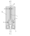
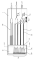
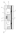
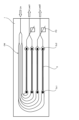
本発明は、図3乃至8に示すように、1つの光波を2つに分岐する分岐導波路を少なくとも含む光導波路OWと、該分岐導波路に電界を印加するための制御電極とを有する光制御基板1と、該制御電極に印加される電気信号を中継する配線又は該電気信号を終端する配線を設けた配線基板(20,21)とを備えた光変調器において、該制御電極が信号電極Sを備え、該配線が信号配線を備え、図4に示すように、該信号電極と該信号配線とを電気的に接続する部分(信号電極側はSc)においては、該分岐導波路が該信号電極を挟む間隔W1は、該制御電極が該分岐導波路に電界を印加する作用部分(符号A)における該分岐導波路が該信号電極を挟む間隔W2よりも広くなっていることを特徴とする。
光変調器において、光制御基板1に隣接して制御電極に印加する電気信号を発生するドライバ回路素子DRVが配置され、該ドライバ回路素子の出力端子は、上述した配線基板20の配線に接続される。図9の光制御基板1には、光ファイバーFを用いて、レンズ等の光学部品を介して入力光Linが入力される。他方、光制御基板1から出射した光波は、例えば、偏波合成手段PCを経て合成され、レンズ等の光学部品を介して、別の光ファイバーに入力され、出力光Loutとなる。
20 配線基板(中継基板)
21 配線基板(終端基板)
S 信号電極
Sc 信号電極の接続部分
GND 接地電極
Gc 接地電極の接続部分
OW 光導波路
Claims (7)
- 1つの光波を2つに分岐する分岐導波路を少なくとも含む光導波路と、該分岐導波路に電界を印加するための制御電極とを有する光制御基板と、
該制御電極に印加される変調信号を中継する配線を設けた配線基板を備えた光変調器において、
該制御電極が信号電極及び該信号電極を挟む接地電極とを備え、
該配線が信号配線と接地配線とを備え、
該信号電極と該信号配線とを電気的に接続する部分においては、該信号電極は前記2つに分岐した該分岐導波路に挟まれており、該分岐導波路が該信号電極を挟む間隔は、該制御電極が該分岐導波路に電界を印加する作用部分における前記2つの分岐した該分岐導波路が該信号電極を挟む間隔よりも広くなっており、
該変調信号の進行方向に対し、該接地電極と該接地配線とが先に電気的に接続され、その後方側で、該信号電極と該信号配線とが電気的に接続されていることを特徴とする光変調器。 - 1つの光波を2つに分岐する分岐導波路を少なくとも含む光導波路と、該分岐導波路に電界を印加するための制御電極とを有する光制御基板と、
該制御電極に印加される変調信号を終端する配線を設けた配線基板を備えた光変調器において、
該制御電極が信号電極及び該信号電極を挟む接地電極とを備え、
該配線が信号配線と接地配線とを備え、
該信号電極と該信号配線とを電気的に接続する部分においては、該信号電極は前記2つに分岐した該分岐導波路に挟まれており、該分岐導波路が該信号電極を挟む間隔は、該制御電極が該分岐導波路に電界を印加する作用部分における前記2つの分岐した該分岐導波路が該信号電極を挟む間隔よりも広くなっており、
該変調信号の進行方向に対し、該信号電極と該信号配線とが先に電気的に接続され、その後方側で、該接地電極と該接地配線とが電気的に接続されていることを特徴とする光変調器。 - 請求項1又は2に記載の光変調器において、該配線基板には、該変調信号を中継する配線と該変調信号を終端する配線とが、共に形成されていることを特徴とする光変調器。
- 請求項1乃至3のいずれかに記載の光変調器において、前記電気的に接続する部分では、フリップチップ接続を用いて電気的接続が行われていることを特徴とする光変調器。
- 請求項1乃至4のいずれかに記載の光変調器において、該光導波路は、凸部の高さが1μm以下の薄板のリブ構造で形成されていることを特徴とする光変調器。
- 請求項1に記載の光変調器において、該光制御基板に隣接して該制御電極に印加する電気信号を発生するドライバ回路素子が配置され、該ドライバ回路素子の出力端子は、該配線基板の配線に接続されていることを特徴とする光変調器。
- 請求項6に記載の光変調器と、該ドライバ回路素子に入力する変調信号を生成する信号発生器とを備えることを特徴とする光送信装置。
Priority Applications (4)
| Application Number | Priority Date | Filing Date | Title |
|---|---|---|---|
| JP2021013606A JP7619060B2 (ja) | 2021-01-29 | 2021-01-29 | 光変調器とそれを用いた光送信装置 |
| PCT/JP2022/002955 WO2022163724A1 (ja) | 2021-01-29 | 2022-01-26 | 光変調器とそれを用いた光送信装置 |
| US18/025,843 US12339529B2 (en) | 2021-01-29 | 2022-01-26 | Optical modulator and optical transmission device using same |
| CN202280006546.0A CN116249930B (zh) | 2021-01-29 | 2022-01-26 | 光调制器及使用其的光发送装置 |
Applications Claiming Priority (1)
| Application Number | Priority Date | Filing Date | Title |
|---|---|---|---|
| JP2021013606A JP7619060B2 (ja) | 2021-01-29 | 2021-01-29 | 光変調器とそれを用いた光送信装置 |
Publications (2)
| Publication Number | Publication Date |
|---|---|
| JP2022117099A JP2022117099A (ja) | 2022-08-10 |
| JP7619060B2 true JP7619060B2 (ja) | 2025-01-22 |
Family
ID=82654666
Family Applications (1)
| Application Number | Title | Priority Date | Filing Date |
|---|---|---|---|
| JP2021013606A Active JP7619060B2 (ja) | 2021-01-29 | 2021-01-29 | 光変調器とそれを用いた光送信装置 |
Country Status (4)
| Country | Link |
|---|---|
| US (1) | US12339529B2 (ja) |
| JP (1) | JP7619060B2 (ja) |
| CN (1) | CN116249930B (ja) |
| WO (1) | WO2022163724A1 (ja) |
Families Citing this family (2)
| Publication number | Priority date | Publication date | Assignee | Title |
|---|---|---|---|---|
| KR102740772B1 (ko) * | 2022-05-04 | 2024-12-10 | 한국전자통신연구원 | 2개 메탈층을 갖는 실리콘 포토닉스 기반 광변조 장치 |
| US20260056368A1 (en) * | 2022-09-30 | 2026-02-26 | Sumitomo Osaka Cement Co., Ltd. | Optical waveguide device, optical modulator, and optical transmission apparatus |
Citations (5)
| Publication number | Priority date | Publication date | Assignee | Title |
|---|---|---|---|---|
| JP2006284838A (ja) | 2005-03-31 | 2006-10-19 | Sumitomo Osaka Cement Co Ltd | 光変調器 |
| JP2011209456A (ja) | 2010-03-29 | 2011-10-20 | Sumitomo Osaka Cement Co Ltd | 光導波路素子モジュール |
| JP2015045790A (ja) | 2013-08-29 | 2015-03-12 | 富士通オプティカルコンポーネンツ株式会社 | 光モジュールおよび光送信機 |
| WO2015193981A1 (ja) | 2014-06-18 | 2015-12-23 | 株式会社日立製作所 | 光変調器およびこれを備えた光送信器、光送受信器 |
| US10788689B1 (en) | 2019-10-18 | 2020-09-29 | National Technology & Engineering Solutions Of Sandia, Llc | Heterogeneously integrated electro-optic modulator |
Family Cites Families (12)
| Publication number | Priority date | Publication date | Assignee | Title |
|---|---|---|---|---|
| US4958898A (en) * | 1989-03-15 | 1990-09-25 | The United States Of America As Represented By The Secretary Of The Air Force | Silicon double-injection electro-optic modulator with insulated-gate and method of using same |
| JP3269654B2 (ja) * | 1992-04-07 | 2002-03-25 | 株式会社日立製作所 | 光電子送受信装置 |
| JP5056040B2 (ja) * | 2007-02-08 | 2012-10-24 | 富士通株式会社 | 光変調器 |
| JP5598221B2 (ja) * | 2010-09-30 | 2014-10-01 | 住友大阪セメント株式会社 | 光制御素子 |
| CN104024926B (zh) * | 2011-12-28 | 2017-03-01 | 住友大阪水泥股份有限公司 | 光波导元件模块 |
| JP5494704B2 (ja) | 2012-03-16 | 2014-05-21 | 住友大阪セメント株式会社 | 光導波路素子モジュール |
| JP6221294B2 (ja) | 2013-03-28 | 2017-11-01 | 住友大阪セメント株式会社 | 光制御素子 |
| JP5835392B2 (ja) * | 2014-03-31 | 2015-12-24 | 住友大阪セメント株式会社 | 光導波路素子モジュール |
| GB2546279B (en) * | 2016-01-12 | 2019-08-21 | Phoelex Ltd | An optical apparatus |
| JP6432574B2 (ja) * | 2016-08-24 | 2018-12-05 | 住友大阪セメント株式会社 | 光変調器、及び光送信装置 |
| US10168596B2 (en) * | 2017-05-23 | 2019-01-01 | Elenion Technoogies, LLC | Optical waveguide modulator |
| US12181279B2 (en) * | 2019-12-11 | 2024-12-31 | Chamartin Laboratories Llc | Optical device for heterodyne interferometry |
-
2021
- 2021-01-29 JP JP2021013606A patent/JP7619060B2/ja active Active
-
2022
- 2022-01-26 CN CN202280006546.0A patent/CN116249930B/zh active Active
- 2022-01-26 WO PCT/JP2022/002955 patent/WO2022163724A1/ja not_active Ceased
- 2022-01-26 US US18/025,843 patent/US12339529B2/en active Active
Patent Citations (5)
| Publication number | Priority date | Publication date | Assignee | Title |
|---|---|---|---|---|
| JP2006284838A (ja) | 2005-03-31 | 2006-10-19 | Sumitomo Osaka Cement Co Ltd | 光変調器 |
| JP2011209456A (ja) | 2010-03-29 | 2011-10-20 | Sumitomo Osaka Cement Co Ltd | 光導波路素子モジュール |
| JP2015045790A (ja) | 2013-08-29 | 2015-03-12 | 富士通オプティカルコンポーネンツ株式会社 | 光モジュールおよび光送信機 |
| WO2015193981A1 (ja) | 2014-06-18 | 2015-12-23 | 株式会社日立製作所 | 光変調器およびこれを備えた光送信器、光送受信器 |
| US10788689B1 (en) | 2019-10-18 | 2020-09-29 | National Technology & Engineering Solutions Of Sandia, Llc | Heterogeneously integrated electro-optic modulator |
Also Published As
| Publication number | Publication date |
|---|---|
| CN116249930B (zh) | 2025-12-12 |
| CN116249930A (zh) | 2023-06-09 |
| JP2022117099A (ja) | 2022-08-10 |
| US12339529B2 (en) | 2025-06-24 |
| US20230350235A1 (en) | 2023-11-02 |
| WO2022163724A1 (ja) | 2022-08-04 |
Similar Documents
| Publication | Publication Date | Title |
|---|---|---|
| US8031987B2 (en) | Optical modulator | |
| JP5598221B2 (ja) | 光制御素子 | |
| JP7196736B2 (ja) | 光導波路素子、及び光導波路デバイス | |
| US20240210784A1 (en) | Optical waveguide element, optical modulator, and optical transmission device | |
| CN217404665U (zh) | 光波导元件、光调制器、光调制模块及光发送装置 | |
| US10088699B2 (en) | Optical modulator | |
| CN116249930B (zh) | 光调制器及使用其的光发送装置 | |
| US20240319558A1 (en) | Optical waveguide element, optical modulator, optical modulation module, and optical transmission device | |
| US20240061309A1 (en) | Optical modulatior and optical transmission device using same | |
| US11442329B2 (en) | Optical waveguide element, optical modulator, optical modulation module, and optical transmission apparatus | |
| US12306478B2 (en) | Optical modulator and optical transmitter | |
| US6768570B2 (en) | Optical modulator | |
| JP7347300B2 (ja) | 光変調器 | |
| JP3695708B2 (ja) | 光変調器 | |
| JP7859487B2 (ja) | 光導波路素子及びそれを用いた光変調デバイス並びに光送信装置 | |
| JP7098930B2 (ja) | 光変調器及びそれを用いた光送信装置 | |
| US12498612B2 (en) | Optical modulator and optical transmission apparatus | |
| US20250355310A1 (en) | Optical waveguide element, and optical transmission apparatus and optical modulation device using optical waveguide element | |
| US20260036866A1 (en) | Optical waveguide element, optical modulator, optical modulation module, and optical transmission device | |
| CN121399531A (zh) | 光波导元件及使用其的光调制器以及光发送装置 | |
| JP2018077545A (ja) | 光送信装置 |
Legal Events
| Date | Code | Title | Description |
|---|---|---|---|
| A621 | Written request for application examination |
Free format text: JAPANESE INTERMEDIATE CODE: A621 Effective date: 20230824 |
|
| A131 | Notification of reasons for refusal |
Free format text: JAPANESE INTERMEDIATE CODE: A131 Effective date: 20240611 |
|
| A521 | Request for written amendment filed |
Free format text: JAPANESE INTERMEDIATE CODE: A523 Effective date: 20240802 |
|
| A131 | Notification of reasons for refusal |
Free format text: JAPANESE INTERMEDIATE CODE: A131 Effective date: 20240827 |
|
| A521 | Request for written amendment filed |
Free format text: JAPANESE INTERMEDIATE CODE: A523 Effective date: 20241025 |
|
| TRDD | Decision of grant or rejection written | ||
| A01 | Written decision to grant a patent or to grant a registration (utility model) |
Free format text: JAPANESE INTERMEDIATE CODE: A01 Effective date: 20241210 |
|
| A61 | First payment of annual fees (during grant procedure) |
Free format text: JAPANESE INTERMEDIATE CODE: A61 Effective date: 20241223 |
|
| R150 | Certificate of patent or registration of utility model |
Ref document number: 7619060 Country of ref document: JP Free format text: JAPANESE INTERMEDIATE CODE: R150 |