JP7347300B2 - 光変調器 - Google Patents
光変調器 Download PDFInfo
- Publication number
- JP7347300B2 JP7347300B2 JP2020062097A JP2020062097A JP7347300B2 JP 7347300 B2 JP7347300 B2 JP 7347300B2 JP 2020062097 A JP2020062097 A JP 2020062097A JP 2020062097 A JP2020062097 A JP 2020062097A JP 7347300 B2 JP7347300 B2 JP 7347300B2
- Authority
- JP
- Japan
- Prior art keywords
- optical
- waveguide
- section
- branching
- electrode
- Prior art date
- Legal status (The legal status is an assumption and is not a legal conclusion. Google has not performed a legal analysis and makes no representation as to the accuracy of the status listed.)
- Active
Links
Images


Classifications
-
- G—PHYSICS
- G02—OPTICS
- G02F—OPTICAL DEVICES OR ARRANGEMENTS FOR THE CONTROL OF LIGHT BY MODIFICATION OF THE OPTICAL PROPERTIES OF THE MEDIA OF THE ELEMENTS INVOLVED THEREIN; NON-LINEAR OPTICS; FREQUENCY-CHANGING OF LIGHT; OPTICAL LOGIC ELEMENTS; OPTICAL ANALOGUE/DIGITAL CONVERTERS
- G02F1/00—Devices or arrangements for the control of the intensity, colour, phase, polarisation or direction of light arriving from an independent light source, e.g. switching, gating or modulating; Non-linear optics
- G02F1/01—Devices or arrangements for the control of the intensity, colour, phase, polarisation or direction of light arriving from an independent light source, e.g. switching, gating or modulating; Non-linear optics for the control of the intensity, phase, polarisation or colour
- G02F1/03—Devices or arrangements for the control of the intensity, colour, phase, polarisation or direction of light arriving from an independent light source, e.g. switching, gating or modulating; Non-linear optics for the control of the intensity, phase, polarisation or colour based on ceramics or electro-optical crystals, e.g. exhibiting Pockels effect or Kerr effect
- G02F1/035—Devices or arrangements for the control of the intensity, colour, phase, polarisation or direction of light arriving from an independent light source, e.g. switching, gating or modulating; Non-linear optics for the control of the intensity, phase, polarisation or colour based on ceramics or electro-optical crystals, e.g. exhibiting Pockels effect or Kerr effect in an optical waveguide structure
- G02F1/0356—Devices or arrangements for the control of the intensity, colour, phase, polarisation or direction of light arriving from an independent light source, e.g. switching, gating or modulating; Non-linear optics for the control of the intensity, phase, polarisation or colour based on ceramics or electro-optical crystals, e.g. exhibiting Pockels effect or Kerr effect in an optical waveguide structure controlled by a high-frequency electromagnetic wave component in an electric waveguide structure
-
- G—PHYSICS
- G02—OPTICS
- G02F—OPTICAL DEVICES OR ARRANGEMENTS FOR THE CONTROL OF LIGHT BY MODIFICATION OF THE OPTICAL PROPERTIES OF THE MEDIA OF THE ELEMENTS INVOLVED THEREIN; NON-LINEAR OPTICS; FREQUENCY-CHANGING OF LIGHT; OPTICAL LOGIC ELEMENTS; OPTICAL ANALOGUE/DIGITAL CONVERTERS
- G02F1/00—Devices or arrangements for the control of the intensity, colour, phase, polarisation or direction of light arriving from an independent light source, e.g. switching, gating or modulating; Non-linear optics
- G02F1/01—Devices or arrangements for the control of the intensity, colour, phase, polarisation or direction of light arriving from an independent light source, e.g. switching, gating or modulating; Non-linear optics for the control of the intensity, phase, polarisation or colour
- G02F1/03—Devices or arrangements for the control of the intensity, colour, phase, polarisation or direction of light arriving from an independent light source, e.g. switching, gating or modulating; Non-linear optics for the control of the intensity, phase, polarisation or colour based on ceramics or electro-optical crystals, e.g. exhibiting Pockels effect or Kerr effect
- G02F1/035—Devices or arrangements for the control of the intensity, colour, phase, polarisation or direction of light arriving from an independent light source, e.g. switching, gating or modulating; Non-linear optics for the control of the intensity, phase, polarisation or colour based on ceramics or electro-optical crystals, e.g. exhibiting Pockels effect or Kerr effect in an optical waveguide structure
-
- G—PHYSICS
- G02—OPTICS
- G02B—OPTICAL ELEMENTS, SYSTEMS OR APPARATUS
- G02B6/00—Light guides; Structural details of arrangements comprising light guides and other optical elements, e.g. couplings
- G02B6/10—Light guides; Structural details of arrangements comprising light guides and other optical elements, e.g. couplings of the optical waveguide type
- G02B6/12—Light guides; Structural details of arrangements comprising light guides and other optical elements, e.g. couplings of the optical waveguide type of the integrated circuit kind
- G02B6/122—Basic optical elements, e.g. light-guiding paths
- G02B6/125—Bends, branchings or intersections
-
- G—PHYSICS
- G02—OPTICS
- G02F—OPTICAL DEVICES OR ARRANGEMENTS FOR THE CONTROL OF LIGHT BY MODIFICATION OF THE OPTICAL PROPERTIES OF THE MEDIA OF THE ELEMENTS INVOLVED THEREIN; NON-LINEAR OPTICS; FREQUENCY-CHANGING OF LIGHT; OPTICAL LOGIC ELEMENTS; OPTICAL ANALOGUE/DIGITAL CONVERTERS
- G02F1/00—Devices or arrangements for the control of the intensity, colour, phase, polarisation or direction of light arriving from an independent light source, e.g. switching, gating or modulating; Non-linear optics
- G02F1/01—Devices or arrangements for the control of the intensity, colour, phase, polarisation or direction of light arriving from an independent light source, e.g. switching, gating or modulating; Non-linear optics for the control of the intensity, phase, polarisation or colour
- G02F1/03—Devices or arrangements for the control of the intensity, colour, phase, polarisation or direction of light arriving from an independent light source, e.g. switching, gating or modulating; Non-linear optics for the control of the intensity, phase, polarisation or colour based on ceramics or electro-optical crystals, e.g. exhibiting Pockels effect or Kerr effect
- G02F1/0305—Constructional arrangements
- G02F1/0316—Electrodes
-
- G—PHYSICS
- G02—OPTICS
- G02F—OPTICAL DEVICES OR ARRANGEMENTS FOR THE CONTROL OF LIGHT BY MODIFICATION OF THE OPTICAL PROPERTIES OF THE MEDIA OF THE ELEMENTS INVOLVED THEREIN; NON-LINEAR OPTICS; FREQUENCY-CHANGING OF LIGHT; OPTICAL LOGIC ELEMENTS; OPTICAL ANALOGUE/DIGITAL CONVERTERS
- G02F1/00—Devices or arrangements for the control of the intensity, colour, phase, polarisation or direction of light arriving from an independent light source, e.g. switching, gating or modulating; Non-linear optics
- G02F1/01—Devices or arrangements for the control of the intensity, colour, phase, polarisation or direction of light arriving from an independent light source, e.g. switching, gating or modulating; Non-linear optics for the control of the intensity, phase, polarisation or colour
- G02F1/21—Devices or arrangements for the control of the intensity, colour, phase, polarisation or direction of light arriving from an independent light source, e.g. switching, gating or modulating; Non-linear optics for the control of the intensity, phase, polarisation or colour by interference
- G02F1/212—Mach-Zehnder type
Landscapes
- Physics & Mathematics (AREA)
- Nonlinear Science (AREA)
- General Physics & Mathematics (AREA)
- Optics & Photonics (AREA)
- Engineering & Computer Science (AREA)
- Chemical & Material Sciences (AREA)
- Ceramic Engineering (AREA)
- Crystallography & Structural Chemistry (AREA)
- Electromagnetism (AREA)
- Microelectronics & Electronic Packaging (AREA)
- Optical Modulation, Optical Deflection, Nonlinear Optics, Optical Demodulation, Optical Logic Elements (AREA)
Description
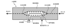
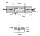
(1) 基板に、光導波路と、該光導波路を伝搬する光波を変調する変調電極とを形成し、該基板を筐体内に収容した光変調器において、該光導波路は、1つの光波を2つに分岐する光分岐部又は2つの光波を1つに合波する光合波部を少なくとも備え、該変調電極は、信号電極と接地電極とを有すると共に、該信号電極の一部が該光分岐部又は該光合波部を横切るように配置され、該光分岐部又は該光合波部を横切る該信号電極によって、該光分岐部で分岐する光波の強度比又は該光合波部で合波する光波の強度比が変化することを抑制するための抑制手段を備え、該抑制手段は、該光分岐部又は該光合波部と、該変調電極との間に設けられた樹脂層であり、該樹脂層は、該変調電極が形成する電界が該光導波路に作用する作用部には形成されていないことを特徴とする。
本発明の光変調器は、図6、7、9、11又は12に示すような、光導波路の光分岐部又は光合波部を信号電極が横切るよう構成された光変調器を対象としている。
具体的には、図6などに示すように、基板に、光導波路と、該光導波路を伝搬する光波を変調する変調電極とを形成し、図8又は10に示すように、該基板を筐体内に収容した光変調器において、該光導波路は、1つの光波を2つに分岐する光分岐部又は2つの光波を1つに合波する光合波部を少なくとも備え、該変調電極は、信号電極と接地電極とを有すると共に、該信号電極の一部が該光分岐部又は該光合波部を横切るように配置され、該光分岐部又は該光合波部を横切る該信号電極によって、該光分岐部で分岐する光波の強度比又は該光合波部で合波する光波の強度比が変化することを抑制するための抑制手段を備えたことを特徴とする。
Claims (5)
- 基板に、光導波路と、該光導波路を伝搬する光波を変調する変調電極とを形成し、該基板を筐体内に収容した光変調器において、
該光導波路は、1つの光波を2つに分岐する光分岐部又は2つの光波を1つに合波する光合波部を少なくとも備え、
該変調電極は、信号電極と接地電極とを有すると共に、該信号電極の一部が該光分岐部又は該光合波部を横切るように配置され、
該光分岐部又は該光合波部を横切る該信号電極によって、該光分岐部で分岐する光波の強度比又は該光合波部で合波する光波の強度比が変化することを抑制するための抑制手段を備え、
該抑制手段は、該光分岐部又は該光合波部と、該変調電極との間に設けられた樹脂層であり、該樹脂層は、該変調電極が形成する電界が該光導波路に作用する作用部には形成されていないことを特徴とする光変調器。 - 請求項1に記載の光変調器において、該筐体に設けられ、該変調電極に電気信号を供給するインターフェース部は、該光分岐部又は該光合波部を通過する光波の伝搬方向であり該光分岐部又は該光合波部の線対称軸の延長線と、該筐体の側面とが交差する位置の近傍に形成されていることを特徴とする光変調器。
- 請求項1又は2に記載の光変調器において、該光分岐部又は該光合波部はY分岐部で構成され、
該Y分岐部は、シングルモードに対応する導波路幅Wを有する1本の入出力用導波路と、該入出力用導波路に接続し、導波路幅が前記Wよりも広い導波路幅で形成される変換用導波路と、該変換用導波路に接続する2つの分岐用導波路を有し、
該信号電極が該光分岐部又は該光合波部を横切る位置は、該変換用導波路又は、該変換用導波路から2つの該分岐用導波路の距離が該分岐用導波路を伝搬する光波のモードフィールド径の3倍まで離れるまでの範囲以内の該分岐用導波路の何れかであることを特徴とする光変調器。 - 請求項1に記載の光変調器において、変調電極と樹脂層とが重なった部分の長さは、変調信号の波長の10分の1以下に設定されていることを特徴とする光変調器。
- 基板に、光導波路と、該光導波路を伝搬する光波を変調する変調電極とを形成し、該基板を筐体内に収容した光変調器において、
該光導波路は、1つの光波を2つに分岐する光分岐部又は2つの光波を1つに合波する光合波部を少なくとも備え、
該変調電極は、信号電極と接地電極とを有すると共に、該信号電極の一部が該光分岐部又は該光合波部を横切るように配置され、
該光分岐部又は該光合波部を横切る該信号電極によって、該光分岐部で分岐する光波の強度比又は該光合波部で合波する光波の強度比が変化することを抑制するための抑制手段を備え、
該抑制手段は、該光分岐部又は該光合波部を通過する光波の伝搬方向であり該光分岐部又は該光合波部の線対称軸に沿って配置され、該線対称軸に対して対称な形状を有し、該信号電極が該光分岐部又は該光合波部を横切る位置では、該信号電極の幅が該分岐用導波路を伝搬する光波のモードフィールド径の3倍以上であることを特徴とする光変調器。
Priority Applications (4)
| Application Number | Priority Date | Filing Date | Title |
|---|---|---|---|
| JP2020062097A JP7347300B2 (ja) | 2020-03-31 | 2020-03-31 | 光変調器 |
| CN202110076101.7A CN113534507B (zh) | 2020-03-31 | 2021-01-20 | 光调制器 |
| CN202120156854.4U CN215375995U (zh) | 2020-03-31 | 2021-01-20 | 光调制器 |
| US17/170,034 US11493788B2 (en) | 2020-03-31 | 2021-02-08 | Optical modulator |
Applications Claiming Priority (1)
| Application Number | Priority Date | Filing Date | Title |
|---|---|---|---|
| JP2020062097A JP7347300B2 (ja) | 2020-03-31 | 2020-03-31 | 光変調器 |
Publications (2)
| Publication Number | Publication Date |
|---|---|
| JP2021162640A JP2021162640A (ja) | 2021-10-11 |
| JP7347300B2 true JP7347300B2 (ja) | 2023-09-20 |
Family
ID=77857450
Family Applications (1)
| Application Number | Title | Priority Date | Filing Date |
|---|---|---|---|
| JP2020062097A Active JP7347300B2 (ja) | 2020-03-31 | 2020-03-31 | 光変調器 |
Country Status (3)
| Country | Link |
|---|---|
| US (1) | US11493788B2 (ja) |
| JP (1) | JP7347300B2 (ja) |
| CN (2) | CN113534507B (ja) |
Families Citing this family (2)
| Publication number | Priority date | Publication date | Assignee | Title |
|---|---|---|---|---|
| JP7347300B2 (ja) * | 2020-03-31 | 2023-09-20 | 住友大阪セメント株式会社 | 光変調器 |
| WO2023117191A1 (en) * | 2021-12-24 | 2023-06-29 | Elstar Dynamics Patents B.V. | Substrate comprising electrodes and light modulator with reduced diffraction |
Citations (8)
| Publication number | Priority date | Publication date | Assignee | Title |
|---|---|---|---|---|
| US20020061155A1 (en) | 2000-11-17 | 2002-05-23 | Jian-Jun He | Digital optical switch |
| JP2003202533A (ja) | 2001-12-28 | 2003-07-18 | Ricoh Co Ltd | 有機導波路型光変調器および有機導波路型光変調器の製造方法 |
| JP2012078376A (ja) | 2010-09-30 | 2012-04-19 | Sumitomo Osaka Cement Co Ltd | 光制御素子 |
| JP2014235218A (ja) | 2013-05-31 | 2014-12-15 | 富士通オプティカルコンポーネンツ株式会社 | 光変調器 |
| JP2018028623A (ja) | 2016-08-18 | 2018-02-22 | 住友電気工業株式会社 | 光半導体素子及び光半導体素子の製造方法 |
| CN109164602A (zh) | 2018-09-29 | 2019-01-08 | 深圳市芯思杰智慧传感技术有限公司 | 一种具有改进结构的光波导相位调制器芯片 |
| JP2019174750A (ja) | 2018-03-29 | 2019-10-10 | 住友大阪セメント株式会社 | 光デバイス及びその製造方法 |
| JP2020016717A (ja) | 2018-07-24 | 2020-01-30 | 住友大阪セメント株式会社 | 光導波路素子 |
Family Cites Families (10)
| Publication number | Priority date | Publication date | Assignee | Title |
|---|---|---|---|---|
| JP4911529B2 (ja) * | 2005-02-22 | 2012-04-04 | 日本碍子株式会社 | 光変調器 |
| US7400787B2 (en) * | 2005-04-07 | 2008-07-15 | Photonic Systems, Inc. | Optical modulator with coupled coplanar strip electrode and domain inversion |
| JP2007025371A (ja) * | 2005-07-19 | 2007-02-01 | Ricoh Co Ltd | 有機導波路型光変調器・光通信システム |
| JP2008039859A (ja) * | 2006-08-01 | 2008-02-21 | Fujitsu Ltd | 光変調器 |
| JP5012624B2 (ja) * | 2008-03-31 | 2012-08-29 | 住友大阪セメント株式会社 | 光導波路素子 |
| JP5983256B2 (ja) * | 2012-09-28 | 2016-08-31 | 住友大阪セメント株式会社 | 光変調器 |
| JP6287084B2 (ja) | 2012-11-09 | 2018-03-07 | 住友電気工業株式会社 | 光集積素子、光モジュール |
| JP6056800B2 (ja) * | 2014-03-31 | 2017-01-11 | 住友大阪セメント株式会社 | 光変調器 |
| JP6107869B2 (ja) | 2015-03-31 | 2017-04-05 | 住友大阪セメント株式会社 | 光変調器 |
| JP7347300B2 (ja) * | 2020-03-31 | 2023-09-20 | 住友大阪セメント株式会社 | 光変調器 |
-
2020
- 2020-03-31 JP JP2020062097A patent/JP7347300B2/ja active Active
-
2021
- 2021-01-20 CN CN202110076101.7A patent/CN113534507B/zh active Active
- 2021-01-20 CN CN202120156854.4U patent/CN215375995U/zh not_active Withdrawn - After Issue
- 2021-02-08 US US17/170,034 patent/US11493788B2/en active Active
Patent Citations (8)
| Publication number | Priority date | Publication date | Assignee | Title |
|---|---|---|---|---|
| US20020061155A1 (en) | 2000-11-17 | 2002-05-23 | Jian-Jun He | Digital optical switch |
| JP2003202533A (ja) | 2001-12-28 | 2003-07-18 | Ricoh Co Ltd | 有機導波路型光変調器および有機導波路型光変調器の製造方法 |
| JP2012078376A (ja) | 2010-09-30 | 2012-04-19 | Sumitomo Osaka Cement Co Ltd | 光制御素子 |
| JP2014235218A (ja) | 2013-05-31 | 2014-12-15 | 富士通オプティカルコンポーネンツ株式会社 | 光変調器 |
| JP2018028623A (ja) | 2016-08-18 | 2018-02-22 | 住友電気工業株式会社 | 光半導体素子及び光半導体素子の製造方法 |
| JP2019174750A (ja) | 2018-03-29 | 2019-10-10 | 住友大阪セメント株式会社 | 光デバイス及びその製造方法 |
| JP2020016717A (ja) | 2018-07-24 | 2020-01-30 | 住友大阪セメント株式会社 | 光導波路素子 |
| CN109164602A (zh) | 2018-09-29 | 2019-01-08 | 深圳市芯思杰智慧传感技术有限公司 | 一种具有改进结构的光波导相位调制器芯片 |
Also Published As
| Publication number | Publication date |
|---|---|
| CN113534507A (zh) | 2021-10-22 |
| CN113534507B (zh) | 2026-04-28 |
| US20210302766A1 (en) | 2021-09-30 |
| CN215375995U (zh) | 2021-12-31 |
| US11493788B2 (en) | 2022-11-08 |
| JP2021162640A (ja) | 2021-10-11 |
Similar Documents
| Publication | Publication Date | Title |
|---|---|---|
| US9817294B2 (en) | Optical modulation device | |
| US8078015B2 (en) | Optical modulator | |
| US7787717B2 (en) | Optical waveguide device | |
| JP5212475B2 (ja) | 波長可変光送信機 | |
| JP6056800B2 (ja) | 光変調器 | |
| JP4842987B2 (ja) | 光デバイス | |
| JP5348317B2 (ja) | 光変調装置、光変調装置の駆動方法、及び光変調装置の製造方法 | |
| CN101165583A (zh) | 光调制器和发射器 | |
| CN214795475U (zh) | 光波导元件、使用光波导元件的光调制器件及光发送装置 | |
| JP2006091878A (ja) | アタッチメント型光カップラー装置 | |
| WO2014157456A1 (ja) | 光変調器 | |
| JP7347300B2 (ja) | 光変調器 | |
| US20240319558A1 (en) | Optical waveguide element, optical modulator, optical modulation module, and optical transmission device | |
| US11442329B2 (en) | Optical waveguide element, optical modulator, optical modulation module, and optical transmission apparatus | |
| JPH1172760A (ja) | 光導波路モジュール | |
| JP7619060B2 (ja) | 光変調器とそれを用いた光送信装置 | |
| US20240152021A1 (en) | Optical waveguide element, optical modulator, optical modulation module, and optical transmission device | |
| JP2007094336A (ja) | 光半導体素子および光半導体素子の製造方法 | |
| CN113646692A (zh) | 光调制元件以及光调制模块 | |
| JP6084177B2 (ja) | 光導波路デバイス | |
| JP7172803B2 (ja) | 光デバイス及びそれを用いた光送受信装置 | |
| JP6260631B2 (ja) | 光導波路デバイス | |
| CN118502142B (zh) | 电光调制器 | |
| JP2006243327A (ja) | 光導波路およびこれを用いた光スイッチ | |
| JP2898066B2 (ja) | 光デバイス |
Legal Events
| Date | Code | Title | Description |
|---|---|---|---|
| A621 | Written request for application examination |
Free format text: JAPANESE INTERMEDIATE CODE: A621 Effective date: 20220916 |
|
| A977 | Report on retrieval |
Free format text: JAPANESE INTERMEDIATE CODE: A971007 Effective date: 20230329 |
|
| A131 | Notification of reasons for refusal |
Free format text: JAPANESE INTERMEDIATE CODE: A131 Effective date: 20230404 |
|
| A521 | Request for written amendment filed |
Free format text: JAPANESE INTERMEDIATE CODE: A523 Effective date: 20230605 |
|
| TRDD | Decision of grant or rejection written | ||
| A01 | Written decision to grant a patent or to grant a registration (utility model) |
Free format text: JAPANESE INTERMEDIATE CODE: A01 Effective date: 20230808 |
|
| A61 | First payment of annual fees (during grant procedure) |
Free format text: JAPANESE INTERMEDIATE CODE: A61 Effective date: 20230821 |
|
| R150 | Certificate of patent or registration of utility model |
Ref document number: 7347300 Country of ref document: JP Free format text: JAPANESE INTERMEDIATE CODE: R150 |