JP7667635B2 - Optical film and image display device - Google Patents
Optical film and image display device Download PDFInfo
- Publication number
- JP7667635B2 JP7667635B2 JP2019545206A JP2019545206A JP7667635B2 JP 7667635 B2 JP7667635 B2 JP 7667635B2 JP 2019545206 A JP2019545206 A JP 2019545206A JP 2019545206 A JP2019545206 A JP 2019545206A JP 7667635 B2 JP7667635 B2 JP 7667635B2
- Authority
- JP
- Japan
- Prior art keywords
- optical film
- hard coat
- coat layer
- layer
- inorganic
- Prior art date
- Legal status (The legal status is an assumption and is not a legal conclusion. Google has not performed a legal analysis and makes no representation as to the accuracy of the status listed.)
- Active
Links
Images


Classifications
-
- G—PHYSICS
- G02—OPTICS
- G02B—OPTICAL ELEMENTS, SYSTEMS OR APPARATUS
- G02B1/00—Optical elements characterised by the material of which they are made; Optical coatings for optical elements
- G02B1/10—Optical coatings produced by application to, or surface treatment of, optical elements
- G02B1/14—Protective coatings, e.g. hard coatings
-
- B—PERFORMING OPERATIONS; TRANSPORTING
- B32—LAYERED PRODUCTS
- B32B—LAYERED PRODUCTS, i.e. PRODUCTS BUILT-UP OF STRATA OF FLAT OR NON-FLAT, e.g. CELLULAR OR HONEYCOMB, FORM
- B32B27/00—Layered products comprising a layer of synthetic resin
- B32B27/18—Layered products comprising a layer of synthetic resin characterised by the use of special additives
- B32B27/20—Layered products comprising a layer of synthetic resin characterised by the use of special additives using fillers, pigments, thixotroping agents
-
- B—PERFORMING OPERATIONS; TRANSPORTING
- B32—LAYERED PRODUCTS
- B32B—LAYERED PRODUCTS, i.e. PRODUCTS BUILT-UP OF STRATA OF FLAT OR NON-FLAT, e.g. CELLULAR OR HONEYCOMB, FORM
- B32B7/00—Layered products characterised by the relation between layers; Layered products characterised by the relative orientation of features between layers, or by the relative values of a measurable parameter between layers, i.e. products comprising layers having different physical, chemical or physicochemical properties; Layered products characterised by the interconnection of layers
- B32B7/02—Physical, chemical or physicochemical properties
-
- G—PHYSICS
- G09—EDUCATION; CRYPTOGRAPHY; DISPLAY; ADVERTISING; SEALS
- G09F—DISPLAYING; ADVERTISING; SIGNS; LABELS OR NAME-PLATES; SEALS
- G09F9/00—Indicating arrangements for variable information in which the information is built-up on a support by selection or combination of individual elements
-
- H—ELECTRICITY
- H10—SEMICONDUCTOR DEVICES; ELECTRIC SOLID-STATE DEVICES NOT OTHERWISE PROVIDED FOR
- H10K—ORGANIC ELECTRIC SOLID-STATE DEVICES
- H10K50/00—Organic light-emitting devices
- H10K50/80—Constructional details
- H10K50/84—Passivation; Containers; Encapsulations
- H10K50/844—Encapsulations
-
- H—ELECTRICITY
- H10—SEMICONDUCTOR DEVICES; ELECTRIC SOLID-STATE DEVICES NOT OTHERWISE PROVIDED FOR
- H10K—ORGANIC ELECTRIC SOLID-STATE DEVICES
- H10K50/00—Organic light-emitting devices
- H10K50/80—Constructional details
- H10K50/86—Arrangements for improving contrast, e.g. preventing reflection of ambient light
-
- H—ELECTRICITY
- H10—SEMICONDUCTOR DEVICES; ELECTRIC SOLID-STATE DEVICES NOT OTHERWISE PROVIDED FOR
- H10K—ORGANIC ELECTRIC SOLID-STATE DEVICES
- H10K59/00—Integrated devices, or assemblies of multiple devices, comprising at least one organic light-emitting element covered by group H10K50/00
- H10K59/10—OLED displays
- H10K59/12—Active-matrix OLED [AMOLED] displays
-
- H—ELECTRICITY
- H10—SEMICONDUCTOR DEVICES; ELECTRIC SOLID-STATE DEVICES NOT OTHERWISE PROVIDED FOR
- H10K—ORGANIC ELECTRIC SOLID-STATE DEVICES
- H10K59/00—Integrated devices, or assemblies of multiple devices, comprising at least one organic light-emitting element covered by group H10K50/00
- H10K59/40—OLEDs integrated with touch screens
-
- H—ELECTRICITY
- H10—SEMICONDUCTOR DEVICES; ELECTRIC SOLID-STATE DEVICES NOT OTHERWISE PROVIDED FOR
- H10K—ORGANIC ELECTRIC SOLID-STATE DEVICES
- H10K59/00—Integrated devices, or assemblies of multiple devices, comprising at least one organic light-emitting element covered by group H10K50/00
- H10K59/80—Constructional details
- H10K59/8791—Arrangements for improving contrast, e.g. preventing reflection of ambient light
-
- H—ELECTRICITY
- H10—SEMICONDUCTOR DEVICES; ELECTRIC SOLID-STATE DEVICES NOT OTHERWISE PROVIDED FOR
- H10K—ORGANIC ELECTRIC SOLID-STATE DEVICES
- H10K59/00—Integrated devices, or assemblies of multiple devices, comprising at least one organic light-emitting element covered by group H10K50/00
- H10K59/80—Constructional details
- H10K59/87—Passivation; Containers; Encapsulations
- H10K59/873—Encapsulations
Landscapes
- Physics & Mathematics (AREA)
- General Physics & Mathematics (AREA)
- Optics & Photonics (AREA)
- Engineering & Computer Science (AREA)
- Theoretical Computer Science (AREA)
- Microelectronics & Electronic Packaging (AREA)
- Laminated Bodies (AREA)
- Surface Treatment Of Optical Elements (AREA)
- Devices For Indicating Variable Information By Combining Individual Elements (AREA)
- Electroluminescent Light Sources (AREA)
Description
本願は、先行する日本国出願である特願2017-191319(出願日:2017年9月29日)の優先権の利益を享受するものであり、その開示内容全体は引用することにより本明細書の一部とされる。This application benefits from the priority of an earlier Japanese application, Patent Application No. 2017-191319 (filing date: September 29, 2017), the entire disclosure of which is incorporated herein by reference.
本発明は、光学フィルムおよび画像表示装置に関する。 The present invention relates to an optical film and an image display device.
従来から、スマートフォンやタブレット端末等の画像表示装置には、光学フィルムが用いられている。光学フィルムとして、光透過性基材、ハードコート層、および無機層をこの順で備える光学フィルムを用いることがある(例えば、特許文献1参照)。Optical films have been used in image display devices such as smartphones and tablet terminals. As the optical film, an optical film having a light-transmitting substrate, a hard coat layer, and an inorganic layer in this order may be used (for example, see Patent Document 1).
しかしながら、このような無機層を有する光学フィルムにおいて、無機層の表面に対し♯0000番のスチールウールで1kg/cm2の荷重を加えながら10往復擦るスチールウール試験を行うと、無機層に傷が入ることがあり、または無機層に傷が入るとともにハードコート層が削れることがある。 However, in an optical film having such an inorganic layer, when a steel wool test is performed in which the surface of the inorganic layer is rubbed back and forth 10 times with #0000 steel wool while applying a load of 1 kg/ cm2 , the inorganic layer may be scratched, or the inorganic layer may be scratched and the hard coat layer may be scraped off.
本発明は、上記問題を解決するためになされたものである。すなわち、優れた耐擦傷性を有する光学フィルム、およびこれを備えた画像表示装置を提供することを目的とする。The present invention has been made to solve the above problems. That is, the object is to provide an optical film having excellent scratch resistance, and an image display device including the same.
本発明は、以下の発明を含む。
[1]ハードコート層および無機層をこの順で備える光学フィルムであって、前記ハードコート層が、前記無機層に接し、前記ハードコート層が、バインダ樹脂および無機粒子を含み、前記ハードコート層の膜厚が、1μm以上であり、前記ハードコート層のインデンテーション硬さが、200MPa以上である、光学フィルム。
The present invention includes the following inventions.
[1] An optical film comprising a hard coat layer and an inorganic layer in this order, the hard coat layer being in contact with the inorganic layer, the hard coat layer containing a binder resin and inorganic particles, the hard coat layer having a thickness of 1 μm or more, and an indentation hardness of the hard coat layer being 200 MPa or more.
[2]前記ハードコート層の膜厚方向の断面において、前記ハードコート層と前記無機層の界面から前記ハードコート層の深さ500nmまでの領域における前記無機粒子の面積比率が、5%以上75%以下である、上記[1]に記載の光学フィルム。 [2] An optical film described in [1] above, in which, in a cross section of the hard coat layer in the thickness direction, the area ratio of the inorganic particles in the region from the interface between the hard coat layer and the inorganic layer to a depth of 500 nm in the hard coat layer is 5% or more and 75% or less.
[3]前記無機粒子が、シリカ粒子である、上記[1]または[2]に記載の光学フィルム。 [3] An optical film described in [1] or [2] above, wherein the inorganic particles are silica particles.
[4]光透過性基材、ハードコート層および無機層をこの順で備える光学フィルムであって、前記ハードコート層が、前記無機層に接し、前記ハードコート層が、金属元素および半金属元素の少なくともいずれかを含み、前記ハードコート層の膜厚が、1μm以上であり、前記ハードコート層のインデンテーション硬さが、200MPa以上である、光学フィルム。 [4] An optical film comprising a light-transmitting substrate, a hard coat layer, and an inorganic layer in this order, wherein the hard coat layer is in contact with the inorganic layer, the hard coat layer contains at least one of a metal element and a semi-metal element, the film thickness of the hard coat layer is 1 μm or more, and the indentation hardness of the hard coat layer is 200 MPa or more.
[5]前記無機層が、無機酸化物層である、上記[1]ないし[4]のいずれか一項に記載の光学フィルム。 [5] An optical film described in any one of [1] to [4] above, wherein the inorganic layer is an inorganic oxide layer.
[6]前記無機層が、ケイ素を含む、上記[1]ないし[4]のいずれか一項に記載の光学フィルム。 [6] An optical film described in any one of [1] to [4] above, wherein the inorganic layer contains silicon.
[7]前記無機層の厚みが、10nm以上300nm以下である、上記[1]ないし[6]のいずれか一項に記載の光学フィルム。 [7] An optical film described in any one of [1] to [6] above, wherein the thickness of the inorganic layer is 10 nm or more and 300 nm or less.
[8]前記ハードコート層が半金属元素を含み、前記半金属元素が、ケイ素である、上記[4]ないし[7]のいずれか一項に記載の光学フィルム。 [8] An optical film described in any one of [4] to [7] above, wherein the hard coat layer contains a semi-metal element, and the semi-metal element is silicon.
[9]前記ハードコート層に含まれ、かつX線光電子分光分析法により測定される前記金属元素および前記半金属元素の合計の原子比率が、1.5%以上30%以下である、上記[4]ないし[8]のいずれか一項に記載の光学フィルム。 [9] An optical film described in any one of [4] to [8] above, wherein the total atomic ratio of the metal element and the metalloid element contained in the hard coat layer and measured by X-ray photoelectron spectroscopy is 1.5% or more and 30% or less.
[10]前記ハードコート層が、重合性官能基を有するシルセスキオキサンを含む重合性化合物の重合体を含む、上記[1]ないし[9]のいずれか一項に記載の光学フィルム。 [10] An optical film described in any one of [1] to [9] above, wherein the hard coat layer contains a polymer of a polymerizable compound including a silsesquioxane having a polymerizable functional group.
[11]前記光学フィルムの対向する辺部の間隔が6mmとなるように180°折り畳む試験を10万回繰り返し行った場合に割れまたは破断が生じない、上記[1]ないし[10]のいずれか一項に記載の光学フィルム。 [11] An optical film described in any one of [1] to [10] above, which does not crack or break when a test in which the optical film is folded 180° so that the distance between opposing sides is 6 mm is repeated 100,000 times.
[12]前記無機層が内側となり、かつ前記光学フィルムの対向する辺部の間隔が2mmとなるように180°折り畳む試験を10万回繰り返し行った場合に割れまたは破断が生じない、上記[1]ないし[11]のいずれか一項に記載の光学フィルム。 [12] An optical film described in any one of [1] to [11] above, which does not crack or break when a test in which the optical film is folded 180° with the inorganic layer on the inside and the distance between opposing sides of the optical film is 2 mm is repeated 100,000 times.
[13]前記光透過性基材が、ポリイミド系樹脂、ポリアミド系樹脂、またはこれらの混合物からなる基材である、上記[1]ないし[12]のいずれか一項に記載の光学フィルム。 [13] An optical film described in any one of [1] to [12] above, wherein the light-transmitting substrate is a substrate made of a polyimide-based resin, a polyamide-based resin, or a mixture thereof.
[14]表示パネルと、前記表示パネルよりも観察者側に配置された上記[1]ないし[13]のいずれか一項に記載の光学フィルムと、を備え、前記光学フィルムの前記ハードコート層が、前記光透過性基材よりも観察者側に位置している、画像表示装置。 [14] An image display device comprising a display panel and an optical film described in any one of [1] to [13] above, arranged on the observer side of the display panel, wherein the hard coat layer of the optical film is located on the observer side of the light-transmitting substrate.
[15]前記表示パネルが、有機発光ダイオードパネルである、上記[14]に記載の画像表示装置。 [15] An image display device described in [14] above, wherein the display panel is an organic light-emitting diode panel.
本発明の一の態様および他の態様によれば、優れた耐擦傷性を有する光学フィルムを提供できる。また、本発明の他の態様によれば、このような光学フィルムを備える画像表示装置を提供できる。According to one aspect and another aspect of the present invention, an optical film having excellent scratch resistance can be provided. According to another aspect of the present invention, an image display device including such an optical film can be provided.
[第1の実施形態]
以下、本発明の第1の実施形態に係る光学フィルムおよび画像表示装置について、図面を参照しながら説明する。本明細書において、「フィルム」、「シート」等の用語は、呼称の違いのみに基づいて、互いから区別されるものではない。したがって、例えば、「フィルム」はシートとも呼ばれるような部材も含む意味で用いられる。図1は本実施形態に係る光学フィルムの概略構成図であり、図2は図1に示される光学フィルムの一部の拡大図であり、図3は折り畳み試験の様子を模式的に示した図である。
[First embodiment]
Hereinafter, an optical film and an image display device according to a first embodiment of the present invention will be described with reference to the drawings. In this specification, the terms "film" and "sheet" are not distinguished from each other based only on the difference in name. Therefore, for example, "film" is used to mean a member also called a sheet. FIG. 1 is a schematic diagram of the optical film according to this embodiment, FIG. 2 is an enlarged view of a part of the optical film shown in FIG. 1, and FIG. 3 is a schematic view showing a folding test.
図1に示される光学フィルム10は、光透過性基材11、ハードコート層12、および無機層13をこの順で備えている。ハードコート層12は、無機層13に接している。光学フィルム10は、光透過性基材11とハードコート層12の間に機能層14をさらに備えている。図1に示される光学フィルム10は、機能層14を備えているが、光学フィルムは、機能層を備えていなくともよい。
The
図1においては、光学フィルム10の表面10Aは、無機層13の表面13Aとなっている。なお、本明細書においては、光学フィルムの表面は光学フィルムの片側の表面を意味するものとして用いるので、光学フィルムの表面とは反対側の面は、光学フィルムの表面と区別するために裏面と称するものとする。光学フィルム10の裏面10Bは、光透過性基材11におけるハードコート層12側の面とは反対側の面となっている。In Figure 1,
光学フィルム10のヘイズ値(全ヘイズ値)は2.5%以下であることが好ましい。光学フィルム10のヘイズ値が2.5%以下であれば、優れた透明性を得ることができる。上記ヘイズ値は、1.5%以下、1.0%以下の順にさらに好ましい(数値が小さいほど好ましい)。It is preferable that the haze value (total haze value) of the
上記ヘイズ値は、ヘイズメーター(製品名「HM-150」、村上色彩技術研究所製)を用いてJIS K7136:2000に準拠した方法により測定することができる。上記ヘイズ値は、50mm×100mmの大きさに切り出した後、カールや皺がなく、かつ指紋や埃等がない状態で無機層側が非光源側となるように設置し、光学フィルム1枚に対して3回測定し、3回測定して得られた値の算術平均値とする。本明細書における「3回測定する」とは、同じ場所を3回測定するのではなく、異なる3箇所を測定することを意味するものとする。光学フィルム10においては、目視した表面10Aは平坦であり、かつハードコート層12等の積層する層も平坦であり、また膜厚のばらつきも±10%の範囲内に収まる。したがって、切り出した光学フィルムの異なる3箇所でヘイズ値を測定することで、おおよその光学フィルムの面内全体のヘイズ値の平均値が得られると考えられる。ヘイズ値のばらつきは、測定対象が1m×3000mと長尺であっても、5インチのスマートフォン程度の大きさであっても、±10%以内である。なお、光学フィルムを上記大きさに切り出せない場合には、例えば、HM-150は測定する際の入口開口が20mmφであるので、直径21mm以上となるようなサンプル大きさが必要になる。このため、22mm×22mm以上の大きさに光学フィルムを適宜切り出してもよい。光学フィルムの大きさが小さい場合は、光源スポットが外れない範囲で少しずつずらす、または角度を変えるなどして測定点を3箇所にする。光学フィルムがロール状である場合、光学フィルムは製品(例えば画像表示装置)に使用される部分である有効部分および製品に使用されない部分である非有効部分を有するが、ヘイズ値等の測定のために光学フィルムを切り出す際には光学フィルムの有効部分から切り出すものとする。例えば、光学フィルムの幅方向の両端からそれぞれ5cmまでの部分は、非有効部分となる可能性がある。The haze value can be measured by a method conforming to JIS K7136:2000 using a haze meter (product name "HM-150", manufactured by Murakami Color Research Institute). The haze value is the arithmetic average value of the values obtained by cutting out a piece of optical film in a size of 50 mm x 100 mm, placing the piece so that the inorganic layer side faces the non-light source side without curling or wrinkles and without fingerprints or dust, and measuring three times for each optical film. In this specification, "measured three times" does not mean measuring the same place three times, but measuring three different places. In the
また、光学フィルム10の一方の面側に粘着層や接着層を介して偏光板等の他のフィルムが設けられている場合には、粘着層や接着層とともに他のフィルムを剥離してから、光学フィルムのヘイズ値を求めるものとする。他のフィルムの剥離は、例えば、以下のようにして行うことができる。まず、光学フィルムに粘着層や接着層を介して他のフィルムが付いた積層体をドライヤーで加熱し、光学フィルムと他のフィルムの界面と思われる部位にカッターの刃先を入れて、ゆっくりと剥離していく。このような加熱と剥離を繰り返すことで、粘着層や接着層および他のフィルムを剥離することができる。なお、このような剥離工程があったとしても、ヘイズ値の測定には大きな影響はない。
In addition, when another film such as a polarizing plate is provided on one side of the
光学フィルム10の全光線透過率は、80%以上であることが好ましい。光学フィルム10の全光線透過率が80%以上であれば、充分な光透過性を得ることができる。光学フィルム10の全光線透過率は、85%以上、90%以上の順にさらに好ましい(数値が大きいほど好ましい)。It is preferable that the total light transmittance of the
上記全光線透過率は、ヘイズメーター(製品名「HM-150」、村上色彩技術研究所製)を用いてJIS K7361-1:1997に準拠した方法により測定することができる。上記全光線透過率は、50mm×100mmの大きさに切り出した後、カールや皺がなく、かつ指紋や埃等がない状態で無機層側が非光源側となるように設置し、光学フィルム1枚に対して3回測定し、3回測定して得られた値の算術平均値とする。光学フィルム10においては、目視した表面10Aは平坦であり、かつハードコート層12等の積層する層も平坦であり、また膜厚のばらつきも±10%の範囲内に収まる。したがって、切り出した光学フィルムの異なる3箇所で全光線透過率を測定することで、おおよその光学フィルムの面内全体の全光線透過率の平均値が得られると考えられる。全光線透過率のばらつきは、測定対象が1m×3000mと長尺であっても、5インチのスマートフォン程度の大きさであっても、±10%以内である。なお、光学フィルムを上記大きさに切り出せない場合には、22mm×22mm以上の大きさに光学フィルムを適宜切り出してもよい。光学フィルムの大きさが小さい場合は、光源スポットが外れない範囲で少しずつずらす、または角度を変えるなどして測定点を3箇所にする。The total light transmittance can be measured by a method conforming to JIS K7361-1:1997 using a haze meter (product name "HM-150", manufactured by Murakami Color Research Institute). The total light transmittance is measured three times for each optical film after cutting into a size of 50 mm x 100 mm, without curling or wrinkles, and without fingerprints or dust, so that the inorganic layer side faces the non-light source side, and the arithmetic average value of the values obtained by the three measurements is taken as the total light transmittance. In the
また、光学フィルム10の一方の面側に粘着層や接着層を介して偏光板等の他のフィルムが設けられている場合には、上記と同様の方法によって粘着層や接着層とともに他のフィルムを剥離してから、光学フィルムの全光線透過率とする。なお、このような剥離工程があったとしても、全光線透過率の測定には大きな影響はない。In addition, when another film such as a polarizing plate is provided on one side of the
光学フィルム10のイエローインデックス(YI)は、15以下であることが好ましい。光学フィルム10のイエローインデックスYIが15以下であれば、光学フィルムの黄色味が目立たないので、透明性が求められる用途に適用できる。光学フィルム10のイエローインデックス(YI)の上限は、10以下であることがより好ましい。上記イエローインデックス(YI)は、分光光度計(製品名「UV-3100PC」、島津製作所製、光源:タングステンランプおよび重水素ランプ)を用いて、50mm×100mmの大きさに切り出した光学フィルムについて測定された値からJIS Z8722:2009に記載された演算式に従って色度三刺激値X、Y、Zを計算し、三刺激値X、Y、ZからASTM D1925:1962に記載された演算式に従って算出された値である。上記イエローインデックス(YI)は、光学フィルム1枚に対して3回測定し、3回測定して得られた値の算術平均値とする。The yellow index (YI) of the
また、光学フィルム10の一方の面側に粘着層または接着層を介して偏光板等の他のフィルムが設けられている場合には、上記と同様の方法によって粘着層や接着層とともに他のフィルムを剥離してから、イエローインデックス(YI)を測定するものとする。なお、このような剥離工程があったとしても、イエローインデックス(YI)の測定には大きな影響はない。In addition, when another film such as a polarizing plate is provided on one side of the
光学フィルム10のイエローインデックス(YI)を調整するために、例えば、光透過性基材11やハードコート層12に、黄色の補色となる青色の色素を含有させてもよい。光透過性基材11として、ポリイミド系樹脂からなる基材を用いたことで、黄色味が問題となるような場合であったとしても、光透過性基材11やハードコート層12に青色の色素を含ませることで、光学フィルム10のイエローインデックス(YI)を低下させることができる。In order to adjust the yellow index (YI) of the
上記青色の色素としては、顔料または染料のいずれであってもよいが、例えば、光学フィルム10が有機発光ダイオード表示装置に用いる場合、耐光性や耐熱性を兼ね備えたものが好ましい。上記青色の色素として、多環系有機顔料や金属錯体有機顔料等は、染料の分子分散に比べて紫外線による分子裂断の度合いが少なく耐光性が格段に優れるため、耐光性等が求められる用途に好ましく、より具体的には、フタロシアニン系の有機顔料等が好適に挙げられる。ただし、顔料は溶剤に対して粒子分散するため、粒子散乱による透明性阻害は存在するため、顔料分散体の粒度をレイリー散乱域に入れることが好ましい。一方、光学フィルムの透明性が重要視される場合には、上記青色の色素としては、溶剤に対して分子分散する染料を用いることが好ましい。The blue pigment may be either a pigment or a dye, but for example, when the
光学フィルム10の波長380nmの光の透過率は8%以下であることが好ましい。光学フィルムの上記透過率が8%以下であれば、光学フィルムをモバイル端末に用いた場合、偏光子が紫外線に晒されて、劣化するのを抑制できる。光学フィルム10の上記透過率の上限は5%であることがより好ましい。上記透過率は、分光光度計(製品名「UV-3100PC」、株式会社島津製作所製、光源:タングステンランプおよび重水素ランプ)を用いて測定することができる。上記透過率は、50mm×100mmの大きさに切り出した光学フィルムに対して3回測定し、3回測定して得られた値の算術平均値とする。なお、光学フィルム10の上記透過率は、ハードコート層12中の後述する紫外線吸収剤の添加量を調整すること等によって達成することができる。The transmittance of the
光学フィルム10は、折り畳み性の観点から、光学フィルム10に対し次に説明する折り畳み試験を10万回繰り返し行った場合であっても、光学フィルムに割れまたは破断が生じないことが好ましく、折り畳み試験を20万回繰り返し行った場合であっても、光学フィルム10に割れまたは破断が生じないことがより好ましく、100万回繰り返し行った場合であっても、光学フィルムに割れまたは破断が生じないことがさらに好ましい。光学フィルム10に対し折り畳み試験を10万回繰り返し行った場合に、光学フィルム10に割れ等が生じると、光学フィルム10の折り畳み性が不充分となる。From the viewpoint of foldability, it is preferable that the
光学フィルムの一方の面側に粘着層や接着層を介して偏光板等の他のフィルムが設けられている場合には、光学フィルムの折り畳み試験は、上記と同様の方法によって光学フィルムから粘着層や接着層とともに他のフィルムを剥離した後に行うものとする。また、光学フィルムに粘着層や接着層を介して他のフィルムが付いた積層体に対し折り畳み試験を行った場合には、折り畳み試験を1万回繰り返し行った場合であっても、光学フィルムに割れまたは破断が生じないことが好ましい。 When another film such as a polarizing plate is provided on one side of the optical film via an adhesive layer or bonding layer, the folding test of the optical film is performed after peeling off the other film together with the adhesive layer or bonding layer from the optical film by the same method as above. In addition, when a folding test is performed on a laminate in which another film is attached to an optical film via an adhesive layer or bonding layer, it is preferable that no cracks or breaks occur in the optical film even when the folding test is repeated 10,000 times.
折り畳み試験は、以下のようにして行われる。図3(A)に示すように折り畳み試験においては、まず、20mm×100mmの大きさに切り出した光学フィルム10の辺部10Cと、辺部10Cと対向する辺部10Dとを、平行に配置された固定部20でそれぞれ固定する。なお、光学フィルムを上記大きさに切り出せない場合には、20mm×40mm以上の大きさに光学フィルムを適宜切り出してもよい。また、図3(A)に示すように、固定部20は水平方向にスライド移動可能となっている。The folding test is carried out as follows. As shown in FIG. 3(A), in the folding test, first,
次に、図3(B)に示すように、固定部20を互いに近接するように移動させることで、光学フィルム10の折り畳むように変形させ、更に、図3(C)に示すように、光学フィルム10の固定部20で固定された対向する2つの辺部10C、10Dの間隔が6mmとなる位置まで固定部20を移動させた後、固定部20を逆方向に移動させて光学フィルム10の変形を解消させる。Next, as shown in FIG. 3(B), the fixing
図3(A)~(C)に示すように固定部20を移動させることで、光学フィルム10を180°折り畳むことができる。また、光学フィルム10の屈曲部10Eが固定部20の下端からはみ出さないように折り畳み試験を行い、かつ固定部20が最接近したときの間隔をスペーサー等によって制御することで、光学フィルム10の対向する2つの辺部の間隔を6mmにできる。この場合、屈曲部10Eの外径を6mmとみなす。
As shown in Figures 3(A) to (C), the
また、無機層13が内側となり、かつ光学フィルム10の対向する辺部10C、10Dの間隔が2mmとなるように180°折り畳む試験を10万回繰り返し行った場合に割れまたは破断が生じないことが好ましい。この場合も、光学フィルム10の固定部20で固定された対向する2つの辺部10C、10Dの間隔が2mmとなる位置まで固定部20を移動させた後、固定部20を逆方向に移動させて光学フィルム10の変形を解消させて、折り畳み試験を行うこと以外は、上記と同様に折り畳み試験を行う。
It is also preferable that no cracks or breaks occur when a test in which the
また、光学フィルム10の一方の面側に粘着層や接着層を介して偏光板等の他のフィルムが設けられている場合には、上記と同様の方法によって粘着層や接着層とともに他のフィルムを剥離してから、折り畳み試験を行うものとする。なお、このような剥離工程があったとしても、折り畳み試験には大きな影響はない。In addition, if another film such as a polarizing plate is provided on one side of the
光学フィルム10の表面10Aは、JIS K5600-5-4:1999で規定される鉛筆硬度試験で測定されたときの硬度(鉛筆硬度)が、2H以上であることが好ましい。鉛筆硬度試験は、50mm×100mmの大きさに切り出された光学フィルムの表面に対し鉛筆硬度試験機(製品名「鉛筆引っかき塗膜硬さ試験機(電動式)」、株式会社東洋精機製作所製)を用いて、鉛筆(製品名「ユニ」、三菱鉛筆株式会社製)に750gの荷重を加えながら鉛筆を1mm/秒の移動速度で移動させることにより行うものとする。鉛筆硬度は、鉛筆硬度試験において光学フィルムの表面に傷が付かなかった最も高い硬度とする。なお、鉛筆硬度の測定の際には、硬度が異なる鉛筆を複数本用いて行うが、鉛筆1本につき5回鉛筆硬度試験を行い、5回のうち4回以上光学フィルムの表面に傷が付かなかった場合には、この硬度の鉛筆においては光学フィルムの表面に傷が付かなかったと判断する。上記傷は、鉛筆硬度試験を行った光学フィルムの表面を蛍光灯下で透過観察して視認されるものを指す。光学フィルム10の表面10Aの上記鉛筆硬度は、3H以上であることがより好ましく、5Hであることがさらに好ましく、6H以上であることが最も好ましい。The
近年、パーソナルコンピュータやタブレット端末等の画像表示装置のバックライトの光源として発光ダイオード(Light Emitting Diode)が積極的に採用されているが、この発光ダイオードは、ブルーライトと呼ばれる光を強く発している。このブルーライトは、波長380~495nmの光で紫外線に近い性質を持っており、強いエネルギーを有しているため、角膜や水晶体で吸収されずに網膜に到達することで、網膜の損傷、眼精疲労、睡眠への悪影響等の原因になると言われている。このため、光学フィルムを、画像表示装置に適用した場合に、表示画面の色味に影響を与えることなく、ブルーライト遮蔽性に優れたものとなることが好ましい。このため、ブルーライトを遮光する観点から、光学フィルム10は、波長380nmにおける分光透過率が1%未満であり、波長410nmにおける分光透過率が10%未満であり、波長440nmにおける分光透過率が70%以上であることが好ましい。上記波長380nmにおける分光透過率が1%以上であったり、波長410nmにおける分光透過率が10%以上であったりすると、ブルーライトによる問題を解消できないことがあり、波長440nmにおける分光透過率が70%未満であると、光学フィルムを用いた画像表示装置の表示画面の色味に影響を及ぼしてしまうことがあるからである。光学フィルム10は、ブルーライトの波長のうち、波長410nm以下の波長領域の光を充分に吸収させる一方で、波長440nm以上の光を充分に透過させ、表示画面の色味に影響を与えることなくブルーライトの遮蔽性を優れたものとすることができる。また、このようなブルーライトの遮蔽性に優れる光学フィルム10を画像表示装置として有機発光ダイオード(OLED)表示装置に適用した場合、有機発光ダイオード素子の劣化抑制にも効果的である。In recent years, light-emitting diodes (Light Emitting Diodes) have been actively adopted as light sources for backlights in image display devices such as personal computers and tablet terminals, but these light-emitting diodes strongly emit light called blue light. This blue light has a wavelength of 380 to 495 nm and has properties similar to ultraviolet light. It has strong energy, and is said to cause retinal damage, eye fatigue, and adverse effects on sleep when it reaches the retina without being absorbed by the cornea or crystalline lens. For this reason, when the optical film is applied to an image display device, it is preferable that the optical film has excellent blue light shielding properties without affecting the color of the display screen. For this reason, from the viewpoint of shielding blue light, it is preferable that the
光学フィルム10の光の透過率は、波長380nmまでは殆ど0%であり、波長410nmから徐々に光の透過が大きくなり、波長440nm付近で急激に光の透過が大きくなっていることが好ましい。具体的には、例えば、波長410nmから440nmの間で分光透過率がシグモイド型の曲線を描くように変化することが好ましい。上記波長380nmにおける分光透過率は、より好ましくは0.5%未満、更に好ましくは0.2%未満であり、波長410nmにおける分光透過率がより好ましくは7%未満、より好ましくは5%未満であり、波長440nmにおける分光透過率がより好ましくは75%以上、更に好ましくは80%以上である。なお、光学フィルム10は、波長420nmにおける分光透過率が50%未満であることが好ましい。このような分光透過率の関係を満たすことで、光学フィルム10は、波長440nm付近で急激に透過率が向上するものとなり、表示画面の色味に影響を及ぼすことなく極めて優れたブルーライト遮蔽性を得ることができる。It is preferable that the light transmittance of the
光学フィルム10における波長380nmにおける分光透過率は0.1%未満であることがより好ましく、波長410nmにおける分光透過率は7%未満であることがより好ましく、波長440nmにおける分光透過率は80%以上であることがより好ましい。It is more preferable that the spectral transmittance of the
光学フィルム10は、最小二乗法を用いて得られた波長415~435nmの範囲の透過スペクトルの傾きが2.0より大きいことが好ましい。上記傾きが2.0以下であると、ブルーライトの光波長領域、例えば、波長415~435nmの波長領域において充分に光がカットできずブルーライトカット効果が弱くなることがある。また、ブルーライトの光波長領域(波長415~435nm)をカットしすぎている可能性も考えられ、その場合、画像表示装置のバックライトや発光波長領域(例えば、OLEDの波長430nmからの発光)に干渉してしまい、色味が悪くなるといった不具合が発生する可能性が大きくなることがある。上記傾きは、例えば、0.5nm刻みにて測定可能の分光光度計(製品名「UV-3100PC」、株式会社島津製作所製)を用い、前後1nmの間で最低5ポイント分の透過率のデータを415~435nm間で測定することで算出することができる。It is preferable that the
光学フィルム10は、ブルーライトの遮蔽率が40%以上であることが好ましい。ブルーライトの遮蔽率が40%未満であると、上述したブルーライトに起因した問題が充分に解消できないことがある。上記ブルーライトの遮蔽率は、例えば、JIS T7333:2005により算出される値である。なお、このようなブルーライト遮蔽率は、例えば、ハードコート層12が後述するセサモール型ベンゾトリアゾール系単量体を含むことで、達成することができる。It is preferable that the
光学フィルム10の用途は、特に限定されないが、光学フィルム10の用途としては、例えば、スマートフォン、タブレット端末、パーソナルコンピュータ(PC)、ウェアラブル端末、デジタルサイネージ、テレビジョン、カーナビゲーション等の画像表示装置が挙げられる。また、光学フィルム10は、車載用途にも適している。上記各画像表示装置の形態としては、フォールダブル、ローラブルといったフレキシブル性を必要とする用途にも好ましい。The use of the
光学フィルム10は、所望の大きさにカットされていてもよいが、ロール状であってもよい。光学フィルム10が所望の大きさにカットされている場合、光学フィルムの大きさは、特に制限されず、画像表示装置の表示面の大きさに応じて適宜決定される。具体的には、光学フィルム10の大きさは、例えば、2.8インチ以上500インチ以下となっていてもよい。本明細書における「インチ」とは、光学フィルムが四角形状である場合には対角線の長さを意味し、円形状である場合には直径を意味し、楕円形状である場合には、短径と長径の和の平均値を意味するものとする。ここで、光学フィルムが四角形状である場合、上記インチを求める際の光学フィルムの縦横比は、画像表示装置の表示画面として問題がなければ特に限定されない。例えば、縦:横=1:1、4:3、16:10、16:9、2:1等が挙げられる。ただし、特に、デザイン性に富む車載用途やデジタルサイネージにおいては、このような縦横比に限定されない。また、光学フィルム10の大きさが大きい場合には、任意の位置からA5サイズ(148mm×210mm)に切り出した後、各測定項目の大きさに切り出すものとする。The
画像表示装置における光学フィルム10の配置箇所は、画像表示装置の内部であってもよいが、画像表示装置の表面付近であることが好ましい。画像表示装置の表面付近に用いられる場合、光学フィルム10は、カバーガラスの代わりに用いられるカバーフィルムとして機能する。The
<<光透過性基材>>
光透過性基材11は、光透過性を有する基材である。本明細書における「光透過性」とは、光を透過させる性質を意味し、例えば、全光線透過率が50%以上、好ましくは70%以上、より好ましくは80%以上、特に好ましくは90%以上であることを含む。光透過性とは、必ずしも透明である必要はなく、半透明であってもよい。
<<Light transparent base material>>
The light-transmitting
光透過性基材11の厚みは、10μm以上100μm以下となっていることが好ましい。光透過性基材の厚みが10μm以上であれば、光学フィルム10のカールが抑制でき、また硬度も充分となって鉛筆硬度が3H以上にでき、更に、光学フィルムをRoll to Rollで製造する場合、シワの発生を抑制できるため外観の悪化を招くおそれもない。一方、光透過性基材11の厚みが100μm以下であれば、光学フィルムの折り畳み性能が充分であり、また、軽量化の面で好ましい。光透過性基材の厚みは、走査型電子顕微鏡(SEM)を用いて、光透過性基材の断面を撮影し、その断面の画像において光透過性基材の厚みを10箇所測定し、その10箇所の厚みの算術平均値とする。光透過性基材11の下限は25μm以上であることがより好ましく、光透過性基材11の上限は80μm以下であることがより好ましい。The thickness of the light-transmitting
光透過性基材11の構成材料としては、例えば、ポリイミド系樹脂、ポリアミドイミド系樹脂、ポリアミド系樹脂、ポリエステル系樹脂(例えば、ポリエチレンテレフタレートやポリエチレンナフタレート)等の樹脂が挙げられる。これらの中でも、折り畳み試験において割れ又は破断が発生しにくいだけでなく、優れた硬度及び透明性をも有し、また、耐熱性にも優れ、焼成することにより、更に優れた硬度及び透明性を付与することもできる観点から、ポリイミド系樹脂、ポリアミド系樹脂、またはこれらの混合物が好ましい。Examples of materials constituting the light-transmitting
ポリイミド系樹脂は、テトラカルボン酸成分とジアミン成分とを反応させて得られるものである。ポリイミド系樹脂としては、特に限定されないが、例えば、優れた光透過性および優れた剛性を有する点から、下記一般式(1)および下記一般式(3)で表される構造からなる群から選ばれる少なくとも1種の構造を有することが好ましい。Polyimide resins are obtained by reacting a tetracarboxylic acid component with a diamine component. There are no particular limitations on the polyimide resin, but it is preferable that the polyimide resin has at least one structure selected from the group consisting of structures represented by the following general formula (1) and the following general formula (3), in terms of excellent light transmittance and excellent rigidity.

上記一般式(1)において、R1はテトラカルボン酸残基である4価の基、R2は、trans-シクロヘキサンジアミン残基、trans-1,4-ビスメチレンシクロヘキサンジアミン残基、4,4’-ジアミノジフェニルスルホン残基、3,4’-ジアミノジフェニルスルホン残基、および下記一般式(2)で表される2価の基からなる群から選ばれる少なくとも1種の2価の基を表す。nは繰り返し単位数を表し、1以上である。本明細書において、「テトラカルボン酸残基」とは、テトラカルボン酸から、4つのカルボキシル基を除いた残基をいい、テトラカルボン酸二無水物から酸二無水物構造を除いた残基と同じ構造を表す。また、「ジアミン残基」とは、ジアミンから2つのアミノ基を除いた残基をいう。 In the above general formula (1), R 1 is a tetravalent group which is a tetracarboxylic acid residue, and R 2 is at least one divalent group selected from the group consisting of a trans-cyclohexanediamine residue, a trans-1,4-bismethylenecyclohexanediamine residue, a 4,4'-diaminodiphenylsulfone residue, a 3,4'-diaminodiphenylsulfone residue, and a divalent group represented by the following general formula (2). n represents the number of repeating units and is 1 or more. In this specification, the term "tetracarboxylic acid residue" refers to a residue obtained by removing four carboxyl groups from a tetracarboxylic acid, and represents the same structure as a residue obtained by removing an acid dianhydride structure from a tetracarboxylic dianhydride. In addition, the term "diamine residue" refers to a residue obtained by removing two amino groups from a diamine.
上記一般式(3)において、R5はシクロヘキサンテトラカルボン酸残基、シクロペンタンテトラカルボン酸残基、ジシクロヘキサン-3,4,3’,4’-テトラカルボン酸残基、および4,4'-(ヘキサフルオロイソプロピリデン)ジフタル酸残基からなる群から選ばれる少なくとも1種の4価の基、R6は、ジアミン残基である2価の基を表す。n’は繰り返し単位数を表し、1以上である。 In the above general formula (3), R5 represents at least one tetravalent group selected from the group consisting of a cyclohexanetetracarboxylic acid residue, a cyclopentanetetracarboxylic acid residue, a dicyclohexane-3,4,3',4'-tetracarboxylic acid residue, and a 4,4'-(hexafluoroisopropylidene)diphthalic acid residue, R6 represents a divalent group which is a diamine residue, and n' represents the number of repeating units and is 1 or more.
上記一般式(1)における、R1はテトラカルボン酸残基であり、前記例示されたようなテトラカルボン酸二無水物から酸二無水物構造を除いた残基とすることができる。上記一般式(1)におけるR1としては、中でも、光透過性を向上し、かつ剛性を向上する点から、4,4’-(ヘキサフルオロイソプロピリデン)ジフタル酸残基、3,3’,4,4’-ビフェニルテトラカルボン酸残基、ピロメリット酸残基、2,3’,3,4’-ビフェニルテトラカルボン酸残基、3,3’,4,4’-ベンゾフェノンテトラカルボン酸残基、3,3’,4,4’-ジフェニルスルホンテトラカルボン酸残基、4,4'-オキシジフタル酸残基、シクロヘキサンテトラカルボン酸残基、およびシクロペンタンテトラカルボン酸残基からなる群から選択される少なくとも1種を含むことが好ましく、さらに、4,4’-(ヘキサフルオロイソプロピリデン)ジフタル酸残基、4,4’-オキシジフタル酸残基、および3,3’,4,4’-ジフェニルスルホンテトラカルボン酸残基からなる群から選択される少なくとも1種を含むことが好ましい。 In the above general formula (1), R 1 is a tetracarboxylic acid residue, and can be a residue obtained by removing the acid dianhydride structure from the tetracarboxylic acid dianhydrides exemplified above. As R 1 in the above general formula (1), from the viewpoint of improving light transmittance and improving rigidity, it is preferable to include at least one selected from the group consisting of 4,4'-(hexafluoroisopropylidene)diphthalic acid residue, 3,3',4,4'-biphenyltetracarboxylic acid residue, pyromellitic acid residue, 2,3',3,4'-biphenyltetracarboxylic acid residue, 3,3',4,4'-benzophenonetetracarboxylic acid residue, 3,3',4,4'-diphenylsulfonetetracarboxylic acid residue, 4,4'-oxydiphthalic acid residue, cyclohexanetetracarboxylic acid residue, and cyclopentanetetracarboxylic acid residue, and further, it is preferable to include at least one selected from the group consisting of 4,4'-(hexafluoroisopropylidene)diphthalic acid residue, 4,4'-oxydiphthalic acid residue, and 3,3',4,4'-diphenylsulfonetetracarboxylic acid residue.
R1において、これらの好適な残基を合計で、50モル%以上含むことが好ましく、更に70モル%以上含むことが好ましく、より更に90モル%以上含むことが好ましい。 R1 preferably contains these suitable residues in a total amount of 50 mol % or more, more preferably 70 mol % or more, and even more preferably 90 mol % or more.
また、R1として、3,3’,4,4’-ビフェニルテトラカルボン酸残基、3,3’,4,4’-ベンゾフェノンテトラカルボン酸残基、およびピロメリット酸残基からなる群から選択される少なくとも1種のような剛直性を向上するのに適したテトラカルボン酸残基群(グループA)と、4,4’-(ヘキサフルオロイソプロピリデン)ジフタル酸残基、2,3’,3,4’-ビフェニルテトラカルボン酸残基、3,3’,4,4’-ジフェニルスルホンテトラカルボン酸残基、4,4'-オキシジフタル酸残基、シクロヘキサンテトラカルボン酸残基、およびシクロペンタンテトラカルボン酸残基からなる群から選択される少なくとも1種のような透明性を向上するのに適したテトラカルボン酸残基群(グループB)とを混合して用いることも好ましい。 Also, as R1 , it is preferable to use a mixture of a tetracarboxylic acid residue group (Group A) suitable for improving rigidity, such as at least one selected from the group consisting of 3,3',4,4'-biphenyltetracarboxylic acid residue, 3,3',4,4'-benzophenonetetracarboxylic acid residue, and pyromellitic acid residue, and a tetracarboxylic acid residue group (Group B) suitable for improving transparency, such as at least one selected from the group consisting of 4,4'-(hexafluoroisopropylidene)diphthalic acid residue, 2,3',3,4'-biphenyltetracarboxylic acid residue, 3,3',4,4'-diphenylsulfonetetracarboxylic acid residue, 4,4'-oxydiphthalic acid residue, cyclohexanetetracarboxylic acid residue, and cyclopentanetetracarboxylic acid residue.
この場合、前記剛直性を向上するのに適したテトラカルボン酸残基群(グループA)と、透明性を向上するのに適したテトラカルボン酸残基群(グループB)との含有比率は、透明性を向上するのに適したテトラカルボン酸残基群(グループB)1モルに対して、前記剛直性を向上するのに適したテトラカルボン酸残基群(グループA)が0.05モル以上9モル以下であることが好ましく、更に0.1モル以上5モル以下であることが好ましく、より更に0.3モル以上4モル以下であることが好ましい。In this case, the content ratio of the tetracarboxylic acid residue group suitable for improving the rigidity (Group A) to the tetracarboxylic acid residue group suitable for improving the transparency (Group B) is preferably such that the tetracarboxylic acid residue group suitable for improving the rigidity (Group A) is 0.05 mol or more and 9 mol or less, more preferably 0.1 mol or more and 5 mol or less, and even more preferably 0.3 mol or more and 4 mol or less, per 1 mol of the tetracarboxylic acid residue group suitable for improving the transparency (Group B).
上記一般式(1)におけるR2としては、中でも、光透過性を向上し、かつ剛性を向上する点から、4,4’-ジアミノジフェニルスルホン残基、3,4’-ジアミノジフェニルスルホン残基、および上記一般式(2)で表される2価の基からなる群から選ばれる少なくとも1種の2価の基であることが好ましく、更に、4,4’-ジアミノジフェニルスルホン残基、3,4’-ジアミノジフェニルスルホン残基、ならびに、R3およびR4がパーフルオロアルキル基である上記一般式(2)で表される2価の基からなる群から選ばれる少なくとも1種の2価の基であることが好ましい。 As R2 in the above general formula (1), from the viewpoints of improving light transmittance and improving rigidity, it is preferable that R2 is at least one divalent group selected from the group consisting of 4,4'-diaminodiphenylsulfone residue, 3,4'-diaminodiphenylsulfone residue, and divalent groups represented by the above general formula (2), and further it is preferable that R2 is at least one divalent group selected from the group consisting of 4,4'-diaminodiphenylsulfone residue, 3,4'-diaminodiphenylsulfone residue, and divalent groups represented by the above general formula (2) in which R3 and R4 are perfluoroalkyl groups.
上記一般式(3)におけるR5としては、中でも、光透過性を向上し、かつ剛性を向上する点から、4,4'-(ヘキサフルオロイソプロピリデン)ジフタル酸残基、3,3’,4,4’-ジフェニルスルホンテトラカルボン酸残基、及びオキシジフタル酸残基を含むことが好ましい。 As R5 in the above general formula (3), from the viewpoints of improving light transmittance and improving rigidity, it is preferable to include a 4,4'-(hexafluoroisopropylidene)diphthalic acid residue, a 3,3',4,4'-diphenylsulfonetetracarboxylic acid residue, and an oxydiphthalic acid residue.
R5において、これらの好適な残基を、50モル%以上含むことが好ましく、更に70モル%以上含むことが好ましく、より更に90モル%以上含むことが好ましい。 R5 preferably contains these suitable residues in an amount of 50 mol % or more, more preferably 70 mol % or more, and even more preferably 90 mol % or more.
上記一般式(3)におけるR6はジアミン残基であり、前記例示されたようなジアミンから2つのアミノ基を除いた残基とすることができる。上記一般式(3)におけるR6としては、中でも、光透過性を向上し、かつ剛性を向上する点から、2,2’-ビス(トリフルオロメチル)ベンジジン残基、ビス[4-(4-アミノフェノキシ)フェニル]スルホン残基、4,4’-ジアミノジフェニルスルホン残基、2,2-ビス[4-(4-アミノフェノキシ)フェニル]ヘキサフルオロプロパン残基、ビス[4-(3-アミノフェノキシ)フェニル]スルホン残基、4,4’-ジアミノ-2,2’-ビス(トリフルオロメチル)ジフェニルエーテル残基、1,4-ビス[4-アミノ-2-(トリフルオロメチル)フェノキシ]ベンゼン残基、2,2-ビス[4-(4-アミノ-2-トリフルオロメチルフェノキシ)フェニル]ヘキサフルオロプロパン残基、4,4’-ジアミノ-2-(トリフルオロメチル)ジフェニルエーテル残基、4,4’-ジアミノベンズアニリド残基、N,N’-ビス(4-アミノフェニル)テレフタルアミド残基、及び9,9-ビス(4-アミノフェニル)フルオレン残基からなる群から選ばれる少なくとも1種の2価の基を含むことが好ましく、更に、2,2’-ビス(トリフルオロメチル)ベンジジン残基、ビス[4-(4-アミノフェノキシ)フェニル]スルホン残基、及び4,4’-ジアミノジフェニルスルホン残基からなる群から選ばれる少なくとも1種の2価の基を含むことが好ましい。 R 6 in the above general formula (3) is a diamine residue, and can be a residue obtained by removing two amino groups from the diamines exemplified above. Among them, R 6 in the above general formula (3) can be, from the viewpoint of improving light transmittance and improving rigidity, 2,2'-bis(trifluoromethyl)benzidine residue, bis[4-(4-aminophenoxy)phenyl]sulfone residue, 4,4'-diaminodiphenylsulfone residue, 2,2-bis[4-(4-aminophenoxy)phenyl]hexafluoropropane residue, bis[4-(3-aminophenoxy)phenyl]sulfone residue, 4,4'-diamino-2,2'-bis(trifluoromethyl)diphenyl ether residue, 1,4-bis[4-amino-2-(trifluoromethyl)phenoxy]benzene residue, 2,2-bis[4-(4-amino-2-trifluoromethyl ...4,4'-diamino-2,2'-bis(trifluoromethyl)diphenyl ether residue, 4,4'-diamino-2,2'-bis(trifluoromethyl)diphenyl ether residue, 4,4'-diamino-2,2'-bis(trifluoromethyl)diphenyl ether residue, 4,4'-diamino-2,2 It is preferable that the aryl group contains at least one divalent group selected from the group consisting of a 2,2'-bis(trifluoromethyl)benzidine residue, a bis[4-(4-aminophenoxy)phenyl]hexafluoropropane residue, a 4,4'-diamino-2-(trifluoromethyl)diphenyl ether residue, a 4,4'-diaminobenzanilide residue, an N,N'-bis(4-aminophenyl)terephthalamide residue, and a 9,9-bis(4-aminophenyl)fluorene residue, and it is further preferable that the aryl group contains at least one divalent group selected from the group consisting of a 2,2'-bis(trifluoromethyl)benzidine residue, a bis[4-(4-aminophenoxy)phenyl]sulfone residue, and a 4,4'-diaminodiphenyl sulfone residue.
R6において、これらの好適な残基を合計で、50モル%以上含むことが好ましく、更に70モル%以上含むことが好ましく、より更に90モル%以上含むことが好ましい。 R6 preferably contains these suitable residues in a total amount of 50 mol % or more, more preferably 70 mol % or more, and even more preferably 90 mol % or more.
また、R6として、ビス[4-(4-アミノフェノキシ)フェニル]スルホン残基、4,4’-ジアミノベンズアニリド残基、N,N’-ビス(4-アミノフェニル)テレフタルアミド残基、パラフェニレンジアミン残基、メタフェニレンジアミン残基、および4,4’-ジアミノジフェニルメタン残基からなる群から選択される少なくとも1種のような剛直性を向上するのに適したジアミン残基群(グループC)と、2,2’-ビス(トリフルオロメチル)ベンジジン残基、4,4’-ジアミノジフェニルスルホン残基、2,2-ビス[4-(4-アミノフェノキシ)フェニル]ヘキサフルオロプロパン残基、ビス[4-(3-アミノフェノキシ)フェニル]スルホン残基、4,4’-ジアミノ-2,2’-ビス(トリフルオロメチル)ジフェニルエーテル残基、1,4-ビス[4-アミノ-2-(トリフルオロメチル)フェノキシ]ベンゼン残基、2,2-ビス[4-(4-アミノ-2-トリフルオロメチルフェノキシ)フェニル]ヘキサフルオロプロパン残基、4,4’-ジアミノ-2-(トリフルオロメチル)ジフェニルエーテル残基、及び9,9-ビス(4-アミノフェニル)フルオレン残基からなる群から選択される少なくとも1種のような透明性を向上するのに適したジアミン残基群(グループD)とを混合して用いることも好ましい。 R 6 may be at least one selected from the group consisting of bis[4-(4-aminophenoxy)phenyl]sulfone residue, 4,4'-diaminobenzanilide residue, N,N'-bis(4-aminophenyl)terephthalamide residue, paraphenylenediamine residue, metaphenylenediamine residue, and 4,4'-diaminodiphenylmethane residue, which are suitable for improving rigidity (Group C); and 2,2'-bis(trifluoromethyl)benzidine residue, 4,4'-diaminodiphenylsulfone residue, 2,2-bis[4-(4-aminophenoxy)phenyl]hexafluoropropane residue, bis[4-(3- It is also preferable to use a mixture of at least one diamine residue group (Group D) suitable for improving transparency, such as at least one selected from the group consisting of 4,4'-diamino-2,2'-bis(trifluoromethyl)diphenyl ether residue, 1,4-bis[4-amino-2-(trifluoromethyl)phenoxy]benzene residue, 2,2-bis[4-(4-amino-2-trifluoromethylphenoxy)phenyl]hexafluoropropane residue, 4,4'-diamino-2-(trifluoromethyl)diphenyl ether residue, and 9,9-bis(4-aminophenyl)fluorene residue.
この場合、前記剛直性を向上するのに適したジアミン残基群(グループC)と、透明性を向上するのに適したジアミン残基群(グループD)との含有比率は、透明性を向上するのに適したジアミン残基群(グループD)1モルに対して、前記剛直性を向上するのに適したジアミン残基群(グループC)が0.05モル以上9モル以下であることが好ましく、更に0.1モル以上5モル以下であることが好ましく、0.3モル以上4モル以下であることがより好ましい。In this case, the content ratio of the diamine residue group suitable for improving the rigidity (Group C) to the diamine residue group suitable for improving transparency (Group D) is preferably 0.05 mol or more and 9 mol or less of the diamine residue group suitable for improving the rigidity (Group C) per 1 mol of the diamine residue group suitable for improving transparency (Group D), more preferably 0.1 mol or more and 5 mol or less, and even more preferably 0.3 mol or more and 4 mol or less.
上記一般式(1)および上記一般式(3)で表される構造において、nおよびn’はそれぞれ独立に、繰り返し単位数を表し、1以上である。ポリイミドにおける繰り返し単位数nは、後述する好ましいガラス転移温度を示すように、構造に応じて適宜選択されれば良く、特に限定されない。平均繰り返し単位数は、通常10~2000であり、更に15~1000であることが好ましい。In the structures represented by the above general formula (1) and general formula (3), n and n' each independently represent the number of repeating units and are 1 or more. The number of repeating units in the polyimide, n, may be appropriately selected according to the structure so as to exhibit a preferred glass transition temperature described later, and is not particularly limited. The average number of repeating units is usually 10 to 2000, and more preferably 15 to 1000.
また、ポリイミド系樹脂は、その一部にポリアミド構造を含んでいても良い。含んでいても良いポリアミド構造としては、例えば、トリメリット酸無水物のようなトリカルボン酸残基を含むポリアミドイミド構造や、テレフタル酸のようなジカルボン酸残基を含むポリアミド構造が挙げられる。The polyimide resin may also contain a polyamide structure in part. Examples of the polyamide structure that may be contained include a polyamideimide structure containing a tricarboxylic acid residue such as trimellitic anhydride, and a polyamide structure containing a dicarboxylic acid residue such as terephthalic acid.
ポリイミド系樹脂は、耐熱性の点から、ガラス転移温度が250℃以上であることが好ましく、更に、270℃以上であることが好ましい。一方、延伸の容易さやベーク温度低減の点から、ガラス転移温度が400℃以下であることが好ましく、更に、380℃以下であることが好ましい。From the viewpoint of heat resistance, the polyimide resin preferably has a glass transition temperature of 250°C or higher, and more preferably 270°C or higher. On the other hand, from the viewpoint of ease of stretching and reduction of the bake temperature, the glass transition temperature is preferably 400°C or lower, and more preferably 380°C or lower.
具体的には、ポリイミド系樹脂としては、例えば、下記式で表される構造を有する化合物が挙げられる。下記式中、nは、繰り返し単位であり、2以上の整数を表す。Specifically, examples of polyimide resins include compounds having a structure represented by the following formula: In the formula, n is a repeating unit and represents an integer of 2 or more.
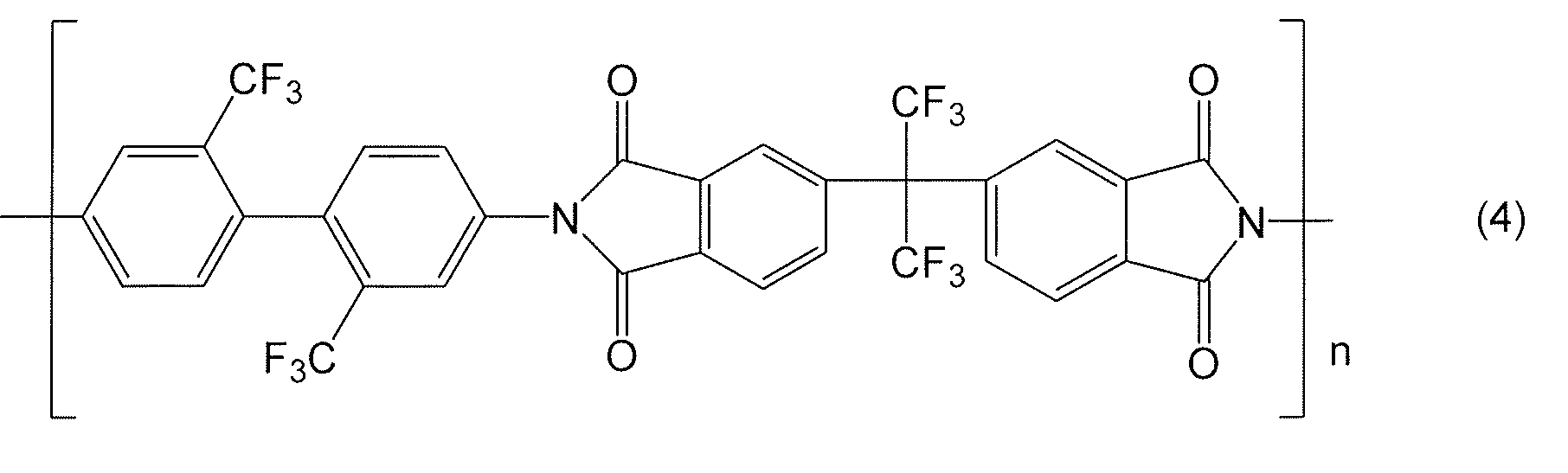


上記ポリイミド系樹脂のなかでも、優れた透明性を有することから、分子内又は分子間の電荷移動が起こりにくい構造を有するポリイミド系樹脂またはポリアミド系樹脂が好ましく、具体的には、上記式(4)~(11)等のフッ素化ポリイミド系樹脂、上記式(13)~(16)等の脂環構造を有するポリイミド系樹脂が挙げられる。Among the above polyimide-based resins, polyimide-based resins or polyamide-based resins having a structure in which intramolecular or intermolecular charge transfer is unlikely to occur are preferred because of their excellent transparency. Specific examples include fluorinated polyimide-based resins such as those represented by the above formulas (4) to (11), and polyimide-based resins having an alicyclic structure such as those represented by the above formulas (13) to (16).
また、上記式(4)~(11)等のフッ素化ポリイミド系樹脂では、フッ素化された構造を有するため、高い耐熱性を有しており、ポリイミド系樹脂からなるポリイミドフィルムの製造時の熱によって着色されることもないので、優れた透明性を有する。 In addition, fluorinated polyimide resins such as those represented by the above formulas (4) to (11) have high heat resistance due to their fluorinated structure, and are not discolored by heat during the production of polyimide films made of polyimide resins, and therefore have excellent transparency.
ポリアミド系樹脂は、脂肪族ポリアミドのみならず、芳香族ポリアミド(アラミド)を含む概念である。ポリアミド系樹脂としては、一般的に、下記式(21)および(22)で表される骨格を有するものであり、上記ポリアミド系樹脂としては、例えば、下記式(23)で表される化合物が挙げられる。なお、下記式中、nは、繰り返し単位であり、2以上の整数を表す。Polyamide-based resins are a concept that includes not only aliphatic polyamides but also aromatic polyamides (aramids). Polyamide-based resins generally have skeletons represented by the following formulas (21) and (22), and examples of the polyamide-based resins include compounds represented by the following formula (23). In the following formula, n is a repeating unit and represents an integer of 2 or more.


上記式(4)~(20)および(23)で表されるポリイミド系樹脂またはポリアミド系樹脂からなる基材は、市販のものを用いても良い。上記ポリイミド系樹脂からなる基材の市販品としては、例えば、三菱ガス化学株式会社製のネオプリム等が挙げられ、上記ポリアミド系樹脂からなる基材の市販品としては、例えば、東レ株式会社製のミクトロン等が挙げられる。The substrate made of the polyimide-based resin or polyamide-based resin represented by the above formulas (4) to (20) and (23) may be commercially available. Examples of commercially available substrates made of the above polyimide-based resin include Neoprim manufactured by Mitsubishi Gas Chemical Company, Inc., and examples of commercially available substrates made of the above polyamide-based resin include Miktron manufactured by Toray Industries, Inc.
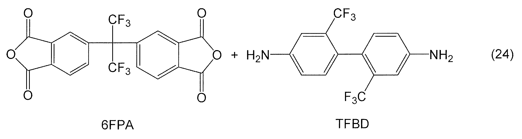
また、上記式(4)~(20)および(23)で表されるポリイミド系樹脂またはポリアミド系樹脂からなる基材は、公知の方法により合成したものを用いても良い。例えば、上記式(4)で表されるポリイミド系樹脂の合成方法は、特開2009-132091に記載されており、具体的には、下記式(24)で表される4,4’-ヘキサフルオロプロピリデンビスフタル酸二無水物(FPA)と2,2’-ビス(トリフルオロメチル)-4,4’-ジアミノビフェニル(TFDB)とを反応させることにより得ることができる。
上記ポリイミド系樹脂またはポリアミド系樹脂の重量平均分子量は、3000以上50万以下の範囲であることが好ましく、5000~30万の範囲であることがより好ましく、1万以上20万以下の範囲であることが更に好ましい。重量平均分子量が3000未満であると、充分な強度が得られないことがあり、50万を超えると粘度が上昇し、溶解性が低下するため、表面が平滑で膜厚が均一な基材が得られないことがある。なお、本明細書において、「重量平均分子量」とは、ゲル浸透クロマトグラフィー(GPC)により測定したポリスチレン換算値である。The weight average molecular weight of the polyimide resin or polyamide resin is preferably in the range of 3,000 to 500,000, more preferably in the range of 5,000 to 300,000, and even more preferably in the range of 10,000 to 200,000. If the weight average molecular weight is less than 3,000, sufficient strength may not be obtained, and if it exceeds 500,000, the viscosity increases and the solubility decreases, so that a substrate with a smooth surface and uniform film thickness may not be obtained. In this specification, the "weight average molecular weight" is a polystyrene-equivalent value measured by gel permeation chromatography (GPC).
上記ポリイミド系樹脂およびポリアミド系樹脂のなかでも、優れた透明性を有することから、分子内又は分子間の電荷移動が起こりにくい構造を有するポリイミド系樹脂またはポリアミド系樹脂が好ましく、具体的には、上記式(4)~(11)等のフッ素化ポリイミド系樹脂、上記式(13)~(16)等の脂環構造を有するポリイミド系樹脂、上記式(23)等のハロゲン基を有するポリアミド系樹脂が挙げられる。Among the above polyimide-based resins and polyamide-based resins, polyimide-based resins or polyamide-based resins having a structure in which intramolecular or intermolecular charge transfer is unlikely to occur are preferred because of their excellent transparency. Specific examples include fluorinated polyimide-based resins such as those represented by the above formulas (4) to (11), polyimide-based resins having alicyclic structures such as those represented by the above formulas (13) to (16), and polyamide-based resins having halogen groups such as those represented by the above formula (23).
また、上記式(4)~(11)等のフッ素化ポリイミド系樹脂では、フッ素化された構造を有するため、高い耐熱性を有しており、ポリイミド系樹脂からなる基材の製造時の熱によって着色されることもないので、優れた透明性を有する。 In addition, fluorinated polyimide resins such as those represented by the above formulas (4) to (11) have high heat resistance due to their fluorinated structure, and are not discolored by heat during the production of substrates made of polyimide resin, and therefore have excellent transparency.
光透過性基材11は、無機層13の表面13AにおけるJIS K5600-5-4:1999に規定される鉛筆硬度試験(荷重:1kg、速度:1mm/秒)の条件で測定された硬度を、3H以上にできることが可能な観点から、上記式(4)~(11)等で表されるフッ素化ポリイミド系樹脂または上記式(23)等のハロゲン基を有するポリアミド系樹脂からなる基材を用いることが好ましい。なかでも、上記鉛筆硬度を3H以上の極めて優れた硬度を付与できることから、上記式(4)で表されるポリイミド系樹脂からなる基材を用いることがより好ましい。From the viewpoint of being able to achieve a hardness of 3H or more measured under the conditions of a pencil hardness test (load: 1 kg, speed: 1 mm/sec) specified in JIS K5600-5-4:1999 on the
ポリエステル系樹脂としては、例えば、ポリエチレンテレフタレート、ポリプロピレンテレフタレート、ポリブチレンテレフタレート、ポリエチレンナフタレートの少なくとも1種を構成成分とする樹脂が挙げられる。Examples of polyester-based resins include resins containing at least one of the following components: polyethylene terephthalate, polypropylene terephthalate, polybutylene terephthalate, and polyethylene naphthalate.
<<ハードコート層>>
ハードコート層12は、200MPa以上のインデンテーション硬さ(HIT)を有する。本明細書における「インデンテーション硬さ」とは、ナノインデンテーション法による硬度測定によって得られる圧子の負荷から除荷までの荷重-変位曲線から求められる値である。ハードコート層12のインデンテーション硬さ(HIT)の下限は、200MPa以上、500MPa以上、800MPa以上の順に好ましい(数値が大きいほど好ましい)。また、ハードコート層12のインデンテーション硬さの上限は、光学フィルム10を折り畳んだ際のハードコート層12の割れやクラックの発生を抑制する観点から、1500MPa以下、1300MPa以下、1100MPa以下の順に好ましい(数値が小さいほど好ましい)。
<<Hard Coat Layer>>
The
上記インデンテーション硬さ(HIT)の測定は、測定サンプルについてHYSITRON(ハイジトロン)社製の「TI950 TriboIndenter」を用いて行うものとする。具体的には、まず、1mm×10mmに切り出した光学フィルムを包埋樹脂によって包埋したブロックを作製し、このブロックから一般的な切片作製方法によって穴等がない均一な、厚さ70nm以上100nm以下の切片を切り出す。切片の作製には、「ウルトラミクロトーム EM UC7」(ライカ マイクロシステムズ株式会社)等を用いることができる。そして、この穴等がない均一な切片が切り出された残りのブロックを測定サンプルとする。次いで、このような測定サンプルにおける上記切片が切り出されることによって得られた断面において、以下の測定条件で、上記圧子としてバーコビッチ(Berkovich)圧子(三角錐、BRUKER社製のTI-0039)をハードコート層の断面に25秒間かけて最大押し込み荷重500μNまでで垂直に押し込む。ここで、バーコビッチ圧子は、光透過性基材や無機層の影響を避けるためおよびハードコート層の側縁の影響を避けるために、光透過性基材とハードコート層の界面からハードコート層の中央側に500nm離れ、ハードコート層と無機層の界面からハードコート層の中央側に500nm離れ、ハードコート層の両側端からそれぞれハードコート層の中央側に500nm離れたハードコート層の部分内に押し込むものとする。なお、光透過性基材とハードコート層の間に機能層が存在する場合には、機能層とハードコート層の界面からハードコート層の中央側に500nm離れ、ハードコート層と無機層の界面からハードコート層の中央側に500nm離れ、ハードコート層の両側端からそれぞれハードコート層の中央側に500nm離れたハードコート層の部分内に押し込むものとする。その後、一定保持して残留応力の緩和を行った後、25秒かけて除荷させて、緩和後の最大荷重を計測し、該最大荷重Pmax(μN)と接触投影面積Ap(nm2)とを用い、Pmax/Apにより、インデンテーション硬さ(HIT)を算出する。上記接触投影面積は、標準試料の溶融石英(BRUKER社製の5-0098)を用いてOliver-Pharr法で圧子先端曲率を補正した接触投影面積である。インデンテーション硬さ(HIT)は、10箇所測定して得られた値の算術平均値とする。なお、測定値の中に算術平均値から±20%以上外れるものが含まれている場合は、その測定値を除外し再測定を行うものとする。測定値の中に算術平均値から±20%以上外れているものが存在するか否かは、測定値をAとし、算術平均値をBとしたとき、(A-B)/B×100によって求められる値(%)が±20%以上であるかによって判断するものとする。インデンテーション硬さ(HIT)は、後述するバインダ樹脂12Aの種類や無機粒子12Bの含有量等によって調整できる。
(測定条件)
・荷重速度:20μN/秒
・保持時間:5秒
・荷重除荷速度:20μN/秒
・測定温度:25℃
The indentation hardness (H IT ) is measured on the measurement sample using a "TI950 TriboIndenter" manufactured by HYSITRON. Specifically, first, a block is prepared by embedding an optical film cut to 1 mm x 10 mm in an embedding resin, and a uniform slice having a thickness of 70 nm to 100 nm without holes is cut out from this block by a general slice preparation method. An "Ultramicrotome EM UC7" (Leica Microsystems, Inc.) or the like can be used to prepare the slice. The remaining block from which the uniform slice without holes is cut out is used as the measurement sample. Next, in the cross section obtained by cutting out the above-mentioned slice from such a measurement sample, a Berkovich indenter (triangular pyramid, TI-0039 manufactured by BRUKER) is pressed vertically into the cross section of the hard coat layer for 25 seconds with a maximum pressing load of 500 μN under the following measurement conditions: Here, in order to avoid the influence of the light-transmitting substrate and the inorganic layer and the influence of the side edges of the hard coat layer, the Berkovich indenter is pressed into a portion of the hard coat layer that is 500 nm away from the interface between the light-transmitting substrate and the hard coat layer toward the center of the hard coat layer, 500 nm away from the interface between the hard coat layer and the inorganic layer toward the center of the hard coat layer, and 500 nm away from each of both side ends of the hard coat layer toward the center of the hard coat layer. In addition, when a functional layer is present between the light-transmitting substrate and the hard coat layer, the hard coat layer is pushed into a portion of the hard coat layer that is 500 nm away from the interface between the functional layer and the hard coat layer toward the center of the hard coat layer, 500 nm away from the interface between the hard coat layer and the inorganic layer toward the center of the hard coat layer, and 500 nm away from each of the two ends of the hard coat layer toward the center of the hard coat layer. After that, the load is removed over 25 seconds to measure the maximum load after relaxation, and the indentation hardness (H IT ) is calculated by P max /A p using the maximum load P max (μN) and the contact projected area A p (nm 2 ). The contact projected area is the contact projected area corrected for the indenter tip curvature by the Oliver-Pharr method using a standard sample of fused quartz (5-0098 manufactured by BRUKER). The indentation hardness (H IT ) is the arithmetic average value of the values obtained by measuring at 10 points. If any of the measured values deviates from the arithmetic mean value by more than ±20%, that measured value shall be excluded and remeasured. Whether or not any of the measured values deviates from the arithmetic mean value by more than ±20% shall be determined by whether the value (%) calculated by (A-B)/Bx100, where A is the measured value and B is the arithmetic mean value, is more than ±20%. The indentation hardness ( HIT ) can be adjusted by the type of
(Measurement conditions)
・Loading speed: 20μN/sec ・Holding time: 5 seconds ・Unloading speed: 20μN/sec ・Measurement temperature: 25℃
ハードコート層12の膜厚は、1μm以上となっている。ハードコート層12の膜厚が、1μm以上であれば、スチールウール試験時にスチールウールのめり込みの程度が少なくなるので、それによってハードコート層の表面の傷付きを抑制できる。ハードコート層12の下限は2μm以上、3μm以上、4μm以上の順にさらに好ましい(数値が大きいほど好ましい)。ハードコート層12の上限は、十分な折り畳み性能を得る観点から、10μm以下、9μm以下、8μm以下、7μm以下の順にさらに好ましい(数値が小さいほど好ましい)。The thickness of the
ハードコート層の膜厚は、走査透過型電子顕微鏡(STEM)、または透過型電子顕微鏡(TEM)を用いて、ハードコート層の断面を撮影し、その断面の画像においてハードコート層の膜厚を10箇所測定し、その10箇所の膜厚の算術平均値とする。具体的な断面写真の撮影方法を以下に記載する。まず、1mm×10mmに切り出した光学フィルムを包埋樹脂によって包埋したブロックを作製し、このブロックから一般的な切片作製方法によって穴等がない均一な、厚さ70nm以上100nm以下の切片を切り出す。切片の作製には、「ウルトラミクロトーム EM UC7」(ライカ マイクロシステムズ株式会社)等を用いることができる。そして、この穴等がない均一な切片を測定サンプルとする。その後、走査透過型電子顕微鏡(STEM)(製品名「S-4800」、株式会社日立ハイテクノロジーズ製)を用いて、測定サンプルの断面写真を撮影する。上記S-4800を用いて断面写真を撮影する際には、検出器を「TE」、加速電圧を「30kV」、エミッション電流を「10μA」にして断面観察を行う。倍率については、フォーカスを調節しコントラストおよび明るさを各層が見分けられるか観察しながら5000倍~20万倍で適宜調節する。好ましい倍率は、1万倍~10万倍、更に好ましい倍率は1万倍~5万倍であり、最も好ましい倍率2.5万倍~5万倍である。なお、上記S-4800を用いて断面写真を撮影する際には、さらに、アパーチャーを「ビームモニタ絞り3」にし、対物レンズ絞りを「3」にし、またW.D.を「8mm」にしてもよい。ハードコート層の膜厚を測定する際には、断面観察した折に、ハードコート層と他の層(例えば、機能層)との界面コントラストが可能な限り明確に観察できることが重要となる。仮に、コントラスト不足でこの界面が見え難い場合には、四酸化オスミウム、四酸化ルテニウム、リンタングステン酸など染色処理を施すと、有機層間の界面が見やすくなるので、染色処理を行ってもよい。また、界面のコントラストは高倍率である方が分かりにくい場合がある。その場合には、低倍率も同時に観察する。例えば、2.5万倍と5万倍や、5万倍と10万倍など、高低の2つの倍率で観察し、両倍率で上記した算術平均値を求め、さらにその平均値をハードコート層の膜厚の値とする。The thickness of the hard coat layer is determined by photographing a cross section of the hard coat layer using a scanning transmission electron microscope (STEM) or a transmission electron microscope (TEM), measuring the thickness of the hard coat layer at 10 points on the image of the cross section, and calculating the arithmetic average value of the thicknesses at the 10 points. A specific method for photographing the cross section is described below. First, a block is prepared by embedding an optical film cut to 1 mm x 10 mm in an embedding resin, and a uniform slice having a thickness of 70 nm to 100 nm without holes is cut from this block using a general slice preparation method. To prepare the slice, an "Ultramicrotome EM UC7" (Leica Microsystems, Inc.) or the like can be used. The uniform slice without holes is used as the measurement sample. Then, a cross section of the measurement sample is photographed using a scanning transmission electron microscope (STEM) (product name "S-4800", manufactured by Hitachi High-Technologies Corporation). When taking a cross-sectional photograph using the S-4800, the detector is set to "TE", the acceleration voltage is set to "30 kV", and the emission current is set to "10 μA" to perform cross-sectional observation. The magnification is adjusted appropriately from 5,000 to 200,000 while adjusting the focus and observing whether the contrast and brightness of each layer can be distinguished. The preferred magnification is 10,000 to 100,000, more preferably 10,000 to 50,000, and most preferably 25,000 to 50,000. When taking a cross-sectional photograph using the S-4800, the aperture may be set to "beam monitor aperture 3", the objective lens aperture to "3", and the WD to "8 mm". When measuring the film thickness of the hard coat layer, it is important that the interface contrast between the hard coat layer and other layers (e.g., functional layers) can be observed as clearly as possible when the cross-section is observed. If the interface is difficult to see due to insufficient contrast, a dyeing process using osmium tetroxide, ruthenium tetroxide, phosphotungstic acid, etc. may be performed to make the interface between the organic layers easier to see. Also, the contrast of the interface may be more difficult to see at higher magnifications. In this case, low magnifications are also observed at the same time. For example, observation is performed at two high and low magnifications, such as 25,000 times and 50,000 times, or 50,000 times and 100,000 times, and the arithmetic average value described above is obtained at both magnifications, and the average value is used as the film thickness value of the hard coat layer.
ハードコート層12は、バインダ樹脂12Aおよび無機粒子12Bを含んでいる。ハードコート層12は、バインダ樹脂12Aおよび無機粒子12Bの他、紫外線吸収剤、分光透過率調整剤のような添加剤を含んでいてもよい。The
図2に示されるハードコート層12の膜厚方向の断面において、ハードコート層12と無機層13の界面IFからハードコート層12の深さ500nmまでの領域IR(以下、この領域を「界面近傍領域」と称することもある。)における無機粒子12Bの面積比率が、5%以上75%以下であることが好ましい。界面近傍領域IFにおける無機粒子の面積比率が5%以上であれば、ハードコート層12中に無機粒子12Bが多く含まれているので、ハードコート層12をより硬くすることができるとともに無機層13との密着性をより向上させることができる。またスチールウール試験は、無機層の表面から荷重を加えた行うものであるが、スチールウールで無機層の表面を擦るために無機層の膜厚方向のみならず、剪断方向にも荷重が加えられる。界面近傍領域IRにおける無機粒子12Bの面積比率が75%以下であれば、スチールウール試験によって剪断方向に荷重が加えられた場合であっても、ハードコート層12中にバインダ樹脂12Aがある程度存在しているので、傷が生じにくく、また削れにくい。また、ハードコート層12中にバインダ樹脂12Aがある程度存在することにより、機能層14との密着性もより向上させることができる。ここで、上記界面近傍領域における無機領域の面積比率を求めることとしたのは、スチールウール試験を行ったときに界面近傍領域が特に傷や削れが生じやすい領域であるからである。上記界面近傍領域IFにおける無機粒子12Bの面積比率の下限は、23%以上、33%以上、44%以上の順にさらに好ましい(数値が大きいほど好ましい)。上記界面近傍領域IFにおける無機粒子12Bの面積比率の上限は、71%以下、67%以下、60%以下の順にさらに好ましい(数値が小さいほど好ましい)。In the cross section of the
上記界面近傍領域における無機粒子の面積比率は、以下のようにして求めるものとする。まず、1mm×10mmに切り出した光学フィルムを包埋樹脂によって包埋したブロックを作製し、このブロックから一般的な切片作製方法によって穴等がない均一な、厚さ70nm以上100nm以下の切片10枚を切り出す。切片の作製には、「ウルトラミクロトーム EM UC7」(ライカ マイクロシステムズ株式会社)等を用いることができる。そして、この穴等がない均一な切片10枚を測定サンプルとする。次いで、透過型電子顕微鏡(TEM)または走査透過型電子顕微鏡(STEM)により各測定サンプルの断面写真を撮影する。なお、測定サンプル1枚につき1箇所の断面写真を撮影するものとする。走査透過型電子顕微鏡(STEM)(製品名「S-4800」、株式会社日立ハイテクノロジーズ製)を用いて、各測定サンプルの断面写真を撮影する場合、この断面写真の撮影の際には、検出器を「TE」、加速電圧を「30kV」、エミッション電流を「10μA」にする。倍率については、フォーカスを調節しコントラストおよび明るさを各層が見分けられるか観察しながら5000倍~20万倍で適宜調節する。好ましい倍率は、1万倍~10万倍、更に好ましい倍率は1万倍~5万倍であり、最も好ましい倍率2.5万倍~5万倍である。なお、断面写真の撮影の際には、さらに、アパーチャーを「ビームモニタ絞り3」にし、対物レンズ絞りを「3」にし、またW.D.を「8mm」にしてもよい。そして、得られた10枚の断面写真において、界面近傍領域の面積を100%とし、界面近傍領域の面積に占める無機粒子の面積の比率(面積比率)を求める。上記界面近傍領域における無機粒子の面積比率は、上記界面近傍領域の10枚の断面写真から求めた無機粒子の面積比率の算術平均値とする。このような無機粒子12Bの面積比率を得るためには、例えば、無機粒子12Bを、硬化後にバインダ樹脂12Aとなる重合性化合物に対して10%以上300%以下、好ましくは10%以上200%の割合(重量比)で含有させることが好ましい。The area ratio of inorganic particles in the region near the interface is determined as follows. First, a block is prepared by embedding an optical film cut to 1 mm x 10 mm in embedding resin, and 10 uniform slices with a thickness of 70 nm to 100 nm are cut out from this block using a general slice preparation method. An "Ultramicrotome EM UC7" (Leica Microsystems) or the like can be used to prepare the slices. These 10 uniform slices without holes are used as measurement samples. Next, a cross-sectional photograph of each measurement sample is taken using a transmission electron microscope (TEM) or a scanning transmission electron microscope (STEM). Note that a cross-sectional photograph is taken at one location per measurement sample. When a cross-sectional photograph of each measurement sample is taken using a scanning transmission electron microscope (STEM) (product name "S-4800", manufactured by Hitachi High-Technologies Corporation), the detector is set to "TE", the acceleration voltage is set to "30 kV", and the emission current is set to "10 μA" when taking the cross-sectional photograph. The magnification is appropriately adjusted from 5,000 to 200,000 times while adjusting the focus and observing whether the contrast and brightness of each layer can be distinguished. A preferred magnification is 10,000 to 100,000 times, a more preferred magnification is 10,000 to 50,000 times, and a most preferred magnification is 25,000 to 50,000 times. When taking the cross-sectional photograph, the aperture may be set to "beam monitor aperture 3", the objective lens aperture to "3", and the W.D. to "8 mm". Then, in the obtained 10 cross-sectional photographs, the area of the interface vicinity region is set to 100%, and the ratio (area ratio) of the area of the inorganic particles to the area of the interface vicinity region is obtained. The area ratio of the inorganic particles in the region near the interface is the arithmetic mean value of the area ratios of the inorganic particles obtained from 10 cross-sectional photographs of the region near the interface. In order to obtain such an area ratio of the
ハードコート層12における無機層13側の面は、バインダ樹脂12Aを選択的にエッチングする方法等によって無機粒子12Bを露出させる処理がされていてもよい。このような処理がされることよって、ハードコート層12と無機層13との密着性をさらに向上させることができる。ただし、この処理を過度に行うと、ハードコート層の表面における無機層側の面が荒れるとともに無機層の膜厚が薄いので、ハードコート層の表面形状が無機層の表面形状に反映させてしまい、スチールウール試験を行ったときに無機層の表面に存在する凹凸でスチールウールが引っ掛かり、耐擦傷性が低下してしまうおそれがある。バインダ樹脂を選択的にエッチングする方法としては、例えば、グロー放電処理、プラズマ処理、イオンエッチング処理、アルカリ処理が挙げられる。The surface of the
<バインダ樹脂>
バインダ樹脂12Aは、重合性化合物(硬化性化合物)の重合体(硬化物)および熱可塑性樹脂の少なくともいずれかを含む。重合性化合物は、分子内にラジカル重合性官能基およびカチオン重合性官能基を少なくとも1つ有するものである。以下、ラジカル重合性官能基を有する重合性化合物をラジカル重合性化合物と称し、カチオン重合性官能基を有する重合性化合物をカチオン重合性化合物と称する。ラジカル重合性官能基としては、例えば、(メタ)アクリロイル基、ビニル基、アリル基等のエチレン性不飽和基が挙げられる。なお、「(メタ)アクリロイル基」とは、「アクリロイル基」および「メタクリロイル基」の両方を含む意味である。カチオン重合性官能基としては、水酸基、カルボキシル基、イソシアネート基、アミノ基、環状エーテル基、メルカプト基等が挙げられる。
<Binder Resin>
The
バインダ樹脂12Aは、重合性官能基当量(重量平均分子量/重合性官能基数)が130以上の重合性化合物を10質量%以上含まないことが好ましい。このような重合性化合物を10質量%以上含まないことにより、ハードコート層12に硬さを付与できるので、光学フィルム10の表面10Aに対しスチールウール試験を行った場合であっても、傷が生じにくく、また削れにくい。また、ハードコート層12と機能層14の密着性もより向上させることができる。It is preferable that the
ラジカル重合性化合物としては、多官能(メタ)アクリレートが好ましい。上記多官能(メタ)アクリレートとしては、例えば、トリメチロールプロパントリ(メタ)アクリレート、トリプロピレングリコールジ(メタ)アクリレート、ジエチレングリコールジ(メタ)アクリレート、ジプロピレングリコールジ(メタ)アクリレート、ペンタエリスリトールトリ(メタ)アクリレート、ペンタエリスリトールテトラ(メタ)アクリレート、ジペンタエリスリトールヘキサ(メタ)アクリレート、1,6-ヘキサンジオールジ(メタ)アクリレート、ネオペンチルグリコールジ(メタ)アクリレート、トリメチロールプロパントリ(メタ)アクリレート、ジトリメチロールプロパンテトラ(メタ)アクリレート、ジペンタエリスリトールペンタ(メタ)アクリレート、トリペンタエリスリトールオクタ(メタ)アクリレート、テトラペンタエリスリトールデカ(メタ)アクリレート、イソシアヌル酸トリ(メタ)アクリレート、イソシアヌル酸ジ(メタ)アクリレート、ポリエステルトリ(メタ)アクリレート、ポリエステルジ(メタ)アクリレート、ビスフェノールジ(メタ)アクリレート、ジグリセリンテトラ(メタ)アクリレート、アダマンチルジ(メタ)アクリレート、イソボロニルジ(メタ)アクリレート、ジシクロペンタンジ(メタ)アクリレート、トリシクロデカンジ(メタ)アクリレート、ジトリメチロールプロパンテトラ(メタ)アクリレートや、これらをPO、EO、カプロラクトン等で変性したものが挙げられる。As the radical polymerizable compound, a polyfunctional (meth)acrylate is preferable. Examples of the polyfunctional (meth)acrylate include trimethylolpropane tri(meth)acrylate, tripropylene glycol di(meth)acrylate, diethylene glycol di(meth)acrylate, dipropylene glycol di(meth)acrylate, pentaerythritol tri(meth)acrylate, pentaerythritol tetra(meth)acrylate, dipentaerythritol hexa(meth)acrylate, 1,6-hexanediol di(meth)acrylate, neopentyl glycol di(meth)acrylate, trimethylolpropane tri(meth)acrylate, ditrimethylolpropane tetra(meth)acrylate, dipentaerythritol penta(meth)acrylate, and the like. acrylate, tripentaerythritol octa(meth)acrylate, tetrapentaerythritol deca(meth)acrylate, isocyanuric acid tri(meth)acrylate, isocyanuric acid di(meth)acrylate, polyester tri(meth)acrylate, polyester di(meth)acrylate, bisphenol di(meth)acrylate, diglycerin tetra(meth)acrylate, adamantyl di(meth)acrylate, isobornyl di(meth)acrylate, dicyclopentane di(meth)acrylate, tricyclodecane di(meth)acrylate, ditrimethylolpropane tetra(meth)acrylate, and those modified with PO, EO, caprolactone, or the like.
これらの中でも上述したインデンテーション硬さを好適に満たし得ることから、3~6官能のものが好ましく、例えば、ペンタエリスリトールトリアクリレート(PETA)、ジペンタエリスリトールヘキサアクリレート(DPHA)、ペンタエリスリトールテトラアクリレート(PETTA)、ジペンタエリスリトールペンタアクリレート(DPPA)、トリメチロールプロパントリ(メタ)アクリレート、トリペンタエリスリトールオクタ(メタ)アクリレート、テトラペンタエリスリトールデカ(メタ)アクリレート等が好ましい。なお、本明細書において、(メタ)アクリレートとは、アクリレート及びメタクリレートを意味する。Among these, those with three to six functionalities are preferred because they can satisfactorily satisfy the above-mentioned indentation hardness, and examples of such preferred compounds include pentaerythritol triacrylate (PETA), dipentaerythritol hexaacrylate (DPHA), pentaerythritol tetraacrylate (PETTA), dipentaerythritol pentaacrylate (DPPA), trimethylolpropane tri(meth)acrylate, tripentaerythritol octa(meth)acrylate, and tetrapentaerythritol deca(meth)acrylate. In this specification, (meth)acrylate means acrylate and methacrylate.
なお、硬度や組成物の粘度調整、密着性の改善等のために、更に単官能(メタ)アクリレートモノマーを含んでいてもよい。上記単官能(メタ)アクリレートモノマーとしては、例えば、ヒドロキシエチルアクリレート(HEA)、グリシジルメタクリレート、メトキシポリエチレングリコール(メタ)アクリレート、イソステアリル(メタ)アクリレート、2-アクリロイルオキシエチルサクシネート、アクリロイルモルホリン、N-アクリロイルオキシエチルヘキサヒドロフタルイミド、シクロヘキシルアクリレート、テトラヒドロフリルアクリレート、イソボルニルアクリレート、フェノキシエチルアクリレート、及び、アダマンチルアクリレート等が挙げられる。In addition, the composition may further contain a monofunctional (meth)acrylate monomer in order to adjust the hardness or viscosity of the composition, improve adhesion, etc. Examples of the monofunctional (meth)acrylate monomer include hydroxyethyl acrylate (HEA), glycidyl methacrylate, methoxypolyethylene glycol (meth)acrylate, isostearyl (meth)acrylate, 2-acryloyloxyethyl succinate, acryloylmorpholine, N-acryloyloxyethylhexahydrophthalimide, cyclohexyl acrylate, tetrahydrofuryl acrylate, isobornyl acrylate, phenoxyethyl acrylate, and adamantyl acrylate.
上記モノマーの重量平均分子量は、ハードコート層12の硬度を向上させる観点から、1000未満が好ましく、200以上800以下がより好ましい。また、上記重合性オリゴマーの重量平均分子量は、1000以上2万以下であることが好ましく、1000以上1万以下であることがより好ましく、2000以上7000以下であることが更に好ましい。From the viewpoint of improving the hardness of the
カチオン重合性化合物としては、特に限定されず、例えば、エポキシ化合物、ポリオール化合物、イソシアネート化合物、メラミン化合物、ウレア化合物、フェノール化合物等が挙げられる。 Cationically polymerizable compounds are not particularly limited and include, for example, epoxy compounds, polyol compounds, isocyanate compounds, melamine compounds, urea compounds, phenol compounds, etc.
熱可塑性樹脂としては、例えば、スチレン系樹脂、(メタ)アクリル系樹脂、酢酸ビニル系樹脂、ビニルエーテル系樹脂、ハロゲン含有樹脂、脂環式オレフィン系樹脂、ポリカーボネート系樹脂、ポリエステル系樹脂、ポリアミド系樹脂、セルロース誘導体、シリコーン系樹脂及びゴム又はエラストマー等を挙げることができる。Examples of thermoplastic resins include styrene-based resins, (meth)acrylic-based resins, vinyl acetate-based resins, vinyl ether-based resins, halogen-containing resins, alicyclic olefin-based resins, polycarbonate-based resins, polyester-based resins, polyamide-based resins, cellulose derivatives, silicone-based resins, and rubber or elastomers.
<無機粒子>
無機粒子12Bは、主として無機物からなる粒子である。無機粒子12Bは、有機成分を含んでいてもよいが、無機物のみから構成されていることが好ましい。無機粒子12Bは、有機成分により表面処理されたものであってもよい。無機粒子12Bとしては、硬度を向上させることができれば、特に限定されないが、優れた硬度を得る観点から、シリカ粒子が好ましい。
<Inorganic particles>
The
シリカ粒子の中でも、反応性シリカ粒子が好ましい。上記反応性シリカ粒子は、上記多官能(メタ)アクリレートとの間で架橋構造を構成することが可能なシリカ粒子であり、この反応性シリカ粒子を含有することで、ハードコート層の硬度を充分に高めることができる。Among the silica particles, reactive silica particles are preferred. The reactive silica particles are silica particles that can form a crosslinked structure with the polyfunctional (meth)acrylate, and the inclusion of these reactive silica particles can sufficiently increase the hardness of the hard coat layer.
上記反応性シリカ粒子は、その表面に反応性官能基を有することが好ましく、該反応性官能基とてしては、例えば、上記の重合性官能基が好適に用いられる。It is preferable that the reactive silica particles have a reactive functional group on their surface, and the reactive functional group is preferably, for example, the polymerizable functional group described above.
上記反応性シリカ粒子としては特に限定されず、従来公知のものを用いることができ、例えば、特開2008-165040号公報記載の反応性シリカ粒子等が挙げられる。また、上記反応性シリカ粒子の市販品としては、例えば、日産化学工業株式会社製のMIBK-SD、MIBK-SDMS、MIBK-SDL、MIBK-SDZL、日揮触媒化成株式会社製のV8802、V8803等が挙げられる。The reactive silica particles are not particularly limited, and conventionally known ones can be used, such as the reactive silica particles described in JP 2008-165040 A. Commercially available reactive silica particles include MIBK-SD, MIBK-SDMS, MIBK-SDL, and MIBK-SDZL manufactured by Nissan Chemical Industries, Ltd., and V8802 and V8803 manufactured by JGC Catalysts and Chemicals Co., Ltd.
また、上記シリカ粒子は、球形シリカ粒子であってもよいが、異形シリカ粒子であることが好ましい。なお、本明細書における「球形シリカ粒子」とは、例えば、真球状、楕円球状等のシリカ粒子を意味しまた、「異形シリカ粒子」とは、ジャガイモ状のランダムな凹凸を表面に有する形状のシリカ粒子を意味する。上記異形シリカ粒子は、その表面積が球形シリカ粒子と比較して大きいため、このような異形シリカ粒子を含有することで、上記多官能(メタ)アクリレート等との接触面積が大きくなり、上記ハードコート層の硬度を向上させることができる。上記異形シリカ粒子か否かは、透過型電子顕微鏡(TEM)または走査透過型電子顕微鏡(STEM)による機能層の断面観察により確認することができる。The silica particles may be spherical, but are preferably irregular silica particles. In this specification, "spherical silica particles" refers to silica particles that are, for example, spherical or elliptical, and "irregular silica particles" refers to silica particles that have random potato-like irregularities on the surface. The irregular silica particles have a larger surface area than spherical silica particles, so that the contact area with the polyfunctional (meth)acrylate, etc. is increased by including such irregular silica particles, thereby improving the hardness of the hard coat layer. Whether the silica particles are irregular or not can be confirmed by observing the cross section of the functional layer using a transmission electron microscope (TEM) or a scanning transmission electron microscope (STEM).
上記シリカ粒子の平均粒子径は、8nm以上100nm以下であることが好ましい。シリカ粒子の平均粒子径が8nm以上であれば、無機層13との密着性を十分に得ることができ、また100nm以下であれば、白化を抑制できる。シリカ粒子の平均粒子径の上限は、65nm以下、40nm以下、25nm以下の順にさらに好ましい(数値が小さいほど好ましい)。シリカ粒子が球形シリカ粒子の場合には、シリカ粒子の平均粒子径は、透過型電子顕微鏡(TEM)または走査透過型電子顕微鏡(STEM)で撮影した画像から、画像処理ソフトウェアを用いて測定される値である。また、シリカ粒子が異形シリカ粒子である場合には、シリカ粒子の平均粒子径は、透過型電子顕微鏡(TEM)または走査透過型電子顕微鏡(STEM)で撮影した画像に現れた異形シリカ粒子の外周の2点間距離の最大値(長径)と最小値(短径)との平均値である。The average particle diameter of the silica particles is preferably 8 nm or more and 100 nm or less. If the average particle diameter of the silica particles is 8 nm or more, sufficient adhesion with the
シリカ粒子としては、2種類以上のシリカ粒子の混合物を用いることが好ましい。例えば、シリカ粒子としては、上記反応性シリカ粒子および非反応性シリカ粒子の混合物や第1のシリカ粒子および粒子径が第1のシリカ粒子よりも小さい第2のシリカ粒子の混合物であってもよい。上記反応性シリカ粒子および非反応性シリカ粒子の混合物を用いた場合には、無機層13との密着性や耐擦傷性を維持しながらカールを抑制できる。また、上記第1のシリカ粒子および第2のシリカ粒子の混合物を用いた場合には、ハードコート層の硬度をさらに向上させることができ、これにより耐擦傷性をより向上させることができる。As the silica particles, it is preferable to use a mixture of two or more types of silica particles. For example, the silica particles may be a mixture of the above-mentioned reactive silica particles and non-reactive silica particles, or a mixture of the first silica particles and the second silica particles having a particle diameter smaller than that of the first silica particles. When the above-mentioned mixture of reactive silica particles and non-reactive silica particles is used, curling can be suppressed while maintaining adhesion and scratch resistance with the
<紫外線吸収剤>
光学フィルムは、屈曲可能なスマートフォンやタブレット端末のようなモバイル端末に特に好適に用いられるが、このようなモバイル端末は屋外で使用されることが多く、そのため、光学フィルムより表示素子側に配置された偏光子が紫外線に晒されて劣化しやすいという問題がある。これに対し、ハードコート層は、偏光子の表示画面側に配置されるため、ハードコート層に紫外線吸収剤が含有されていると、偏光子が紫外線に晒されることによる劣化を好適に防止することができる。
<Ultraviolet absorbing agent>
The optical film is particularly suitable for use in mobile terminals such as bendable smartphones and tablet terminals, but such mobile terminals are often used outdoors, which causes a problem that the polarizer disposed on the display element side of the optical film is easily exposed to ultraviolet light and deteriorates. In contrast, since the hard coat layer is disposed on the display screen side of the polarizer, if the hard coat layer contains an ultraviolet absorbing agent, deterioration of the polarizer due to exposure to ultraviolet light can be suitably prevented.
紫外線吸収剤としては、例えば、トリアジン系紫外線吸収剤、ベンゾフェノン系紫外線吸収剤、及び、ベンゾトリアゾール系紫外線吸収剤等が挙げられる。Examples of ultraviolet absorbers include triazine-based ultraviolet absorbers, benzophenone-based ultraviolet absorbers, and benzotriazole-based ultraviolet absorbers.
上記トリアジン系紫外線吸収剤としては、例えば、2-(2-ヒドロキシ-4-[1-オクチルオキシカルボニルエトキシ]フェニル)-4,6-ビス(4-フェニルフェニル)-1,3,5-トリアジン、2-[4-[(2-ヒドロキシ-3-ドデシルオキシプロピル)オキシ]-2-ヒドロキシフェニル]-4,6-ビス(2,4-ジメチルフェニル)-1,3,5-トリアジン、2,4-ビス[2-ヒドロキシ-4-ブトキシフェニル]-6-(2,4-ジブトキシフェニル)-1,3,5-トリアジン、2-[4-[(2-ヒドロキシ-3-トリデシルオキシプロピル)オキシ]-2-ヒドロキシフェニル]-4,6-ビス(2,4-ジメチルフェニル)-1,3,5-トリアジン、および2-[4-[(2-ヒドロキシ-3-(2’-エチル)ヘキシル)オキシ]-2-ヒドロキシフェニル]-4,6-ビス(2,4-ジメチルフェニル)-1,3,5-トリアジン等が挙げられる。市販されているトリアジン系紫外線吸収剤としては、例えば、TINUVIN460、TINUVIN477(いずれも、BASF社製)、LA-46(株式会社ADEKA製)等が挙げられる。 Examples of the triazine-based ultraviolet absorbers include 2-(2-hydroxy-4-[1-octyloxycarbonylethoxy]phenyl)-4,6-bis(4-phenylphenyl)-1,3,5-triazine, 2-[4-[(2-hydroxy-3-dodecyloxypropyl)oxy]-2-hydroxyphenyl]-4,6-bis(2,4-dimethylphenyl)-1,3,5-triazine, and 2,4-bis[2-hydroxy-4-butoxyphenyl]-6 -(2,4-dibutoxyphenyl)-1,3,5-triazine, 2-[4-[(2-hydroxy-3-tridecyloxypropyl)oxy]-2-hydroxyphenyl]-4,6-bis(2,4-dimethylphenyl)-1,3,5-triazine, and 2-[4-[(2-hydroxy-3-(2'-ethyl)hexyl)oxy]-2-hydroxyphenyl]-4,6-bis(2,4-dimethylphenyl)-1,3,5-triazine. Commercially available triazine-based ultraviolet absorbers include, for example, TINUVIN 460, TINUVIN 477 (both manufactured by BASF), and LA-46 (manufactured by ADEKA Corporation).
上記ベンゾフェノン系紫外線吸収剤としては、例えば、2-ヒドロキシベンゾフェノン、2,4-ジヒドロキシベンゾフェノン、2,2’-ジヒドロキシ-4,4’-ジメトキシベンゾフェノン、2,2’,4,4’-テトラヒドロキシベンゾフェノン、2-ヒドロキシ-4-メトキシベンゾフェノン、ヒドロキシメトキシベンゾフェノンスルホン酸及びその三水塩、ヒドロキシメトキシベンゾフェノンスルホン酸ナトリウム等が挙げられる。市販されているベンゾフェノン系紫外線吸収剤としては、例えば、CHMASSORB81/FL(BASF社製)等が挙げられる。Examples of the benzophenone-based UV absorbers include 2-hydroxybenzophenone, 2,4-dihydroxybenzophenone, 2,2'-dihydroxy-4,4'-dimethoxybenzophenone, 2,2',4,4'-tetrahydroxybenzophenone, 2-hydroxy-4-methoxybenzophenone, hydroxymethoxybenzophenone sulfonic acid and its trihydrate, sodium hydroxymethoxybenzophenone sulfonate, etc. Examples of commercially available benzophenone-based UV absorbers include CHMASSORB81/FL (manufactured by BASF).
上記ベンゾトリアゾール系紫外線吸収剤としては、例えば、2-エチルヘキシル-3-〔3-tert-ブチル-4-ヒドロキシ-5-(5-クロロ-2H-ベンゾトリアゾール-2-イル)フェニル〕プロピオネート、2-(2H-ベンゾトリアゾール-2-イル)-6-(直鎖及び側鎖ドデシル)-4-メチルフェノール、2-〔5-クロロ(2H)-ベンゾトリアゾール-2-イル〕-4-メチル-6-(tert-ブチル)フェノール、2-(2H-ベンゾトリアゾール-2-イル)-4,6-ジ-tert-ペンチルフェノール、2-(2’-ヒドロキシ-5’-メチルフェニル)ベンゾトリアゾール、2-(2’-ヒドロキシ-3’,5’-ジ-tert-ブチルフェニル)ベンゾトリアゾール、2-(2’-ヒドロキシ-3’-tert-ブチル-5’-メチルフェニル)ベンゾトリアゾール、2-(2’-ヒドロキシ-3’,5’-ジ-tert-ブチルフェニル)-5-クロロベンゾトリアゾール、2-(2’-ヒドロキシ-3’-(3’’,4’’,5’’,6’’-テトラヒドロフタルイミドメチル)-5’-メチルフェニル)ベンゾトリアゾール、2,2-メチレンビス(4-(1,1,3,3-テトラメチルブチル)-6-(2H-ベンゾトリアゾール-2-イル)フェノール)、及び、2-(2’-ヒドロキシ-3′-tert-ブチル-5′-メチルフェニル)-5-クロロベンゾトリアゾール等が挙げられる。市販されているベンゾトリアゾール系紫外線吸収剤としては、例えば、KEMISORB71D、KEMISORB79(いずれも、ケミプロ化成株式会社製)、JF-80、JAST-500(いずれも、城北化学工業株式会社製)、ULS-1933D(ライオン・スペシャリティ・ケミカルズ株式会社製)、RUVA-93(大塚化学株式会社製)等が挙げられる。 Examples of the benzotriazole-based ultraviolet absorbers include 2-ethylhexyl-3-[3-tert-butyl-4-hydroxy-5-(5-chloro-2H-benzotriazol-2-yl)phenyl]propionate, 2-(2H-benzotriazol-2-yl)-6-(linear and side chain dodecyl)-4-methylphenol, 2-[5-chloro(2H)-benzotriazol-2-yl]-4-methyl-6-(tert-butyl)phenol, 2-(2H-benzotriazol-2-yl)-4,6-di-tert-pentylphenol, 2-(2'-hydroxy-5'-methylphenyl)benzotriazole, 2-(2'-hydroxy-3',5'-di-tert-butyl) 2-(2'-hydroxy-3'-tert-butyl-5'-methylphenyl)benzotriazole, 2-(2'-hydroxy-3',5'-di-tert-butylphenyl)-5-chlorobenzotriazole, 2-(2'-hydroxy-3'-(3",4",5",6"-tetrahydrophthalimidomethyl)-5'-methylphenyl)benzotriazole, 2,2-methylenebis(4-(1,1,3,3-tetramethylbutyl)-6-(2H-benzotriazol-2-yl)phenol), and 2-(2'-hydroxy-3'-tert-butyl-5'-methylphenyl)-5-chlorobenzotriazole. Examples of commercially available benzotriazole-based ultraviolet absorbers include KEMISORB71D and KEMISORB79 (both manufactured by Chemipro Chemical Co., Ltd.), JF-80 and JAST-500 (both manufactured by Johoku Chemical Co., Ltd.), ULS-1933D (manufactured by Lion Specialty Chemicals Co., Ltd.), and RUVA-93 (manufactured by Otsuka Chemical Co., Ltd.).
紫外線吸収剤は、なかでも、トリアジン系紫外線吸収剤、ベンゾトリアゾール系紫外線吸収剤が好適に用いられる。紫外線吸収剤は、機能層を構成する樹脂成分との溶解性が高いほうが好ましく、また、上述した折り畳み試験後のブリードアウトが少ないほうが好ましい。紫外線吸収剤は、ポリマー化又はオリゴマー化されていることが好ましい。紫外線吸収剤としては、ベンゾトリアゾール、トリアジン、ベンゾフェノン骨格を有するポリマー又はオリゴマーが好ましく、具体的には、ベンゾトリアゾールやベンゾフェノン骨格を有する(メタ)アクリレートと、メチルメタクリレート(MMA)とを任意の比率で熱共重合したものであることが好ましい。なお、有機発光ダイオード(OLED)表示装置に光学フィルムを適用する場合、紫外線吸収剤は、OLEDを紫外線から保護する役割も果たすことができる。Among them, triazine-based ultraviolet absorbers and benzotriazole-based ultraviolet absorbers are preferably used as ultraviolet absorbers. The ultraviolet absorber is preferably highly soluble in the resin components constituting the functional layer, and is preferably less prone to bleed-out after the above-mentioned folding test. The ultraviolet absorber is preferably polymerized or oligomerized. As the ultraviolet absorber, a polymer or oligomer having a benzotriazole, triazine, or benzophenone skeleton is preferable, and specifically, it is preferable that the ultraviolet absorber is a thermal copolymer of a (meth)acrylate having a benzotriazole or benzophenone skeleton and methyl methacrylate (MMA) in any ratio. In addition, when the optical film is applied to an organic light-emitting diode (OLED) display device, the ultraviolet absorber can also play a role in protecting the OLED from ultraviolet rays.
紫外線吸収剤の含有量としては特に限定されないが、機能層用組成物の固形分100質量部に対して1質量部以上6質量部以下であることが好ましい。1質量部未満であると、上述した紫外線吸収剤を機能層に含有させる効果を充分に得ることができないことがあり、6質量部を超えると、機能層に著しい着色や強度低下が生じることがある。上記紫外線吸収剤の含有量のより好ましい下限は2質量部以上、より好ましい上限は5質量部以下である。The content of the ultraviolet absorber is not particularly limited, but is preferably 1 part by mass or more and 6 parts by mass or less per 100 parts by mass of the solid content of the functional layer composition. If it is less than 1 part by mass, the effect of including the ultraviolet absorber in the functional layer may not be fully obtained, and if it exceeds 6 parts by mass, the functional layer may be significantly discolored or have a reduced strength. A more preferable lower limit of the content of the ultraviolet absorber is 2 parts by mass or more, and a more preferable upper limit is 5 parts by mass or less.
<分光透過率調整剤>
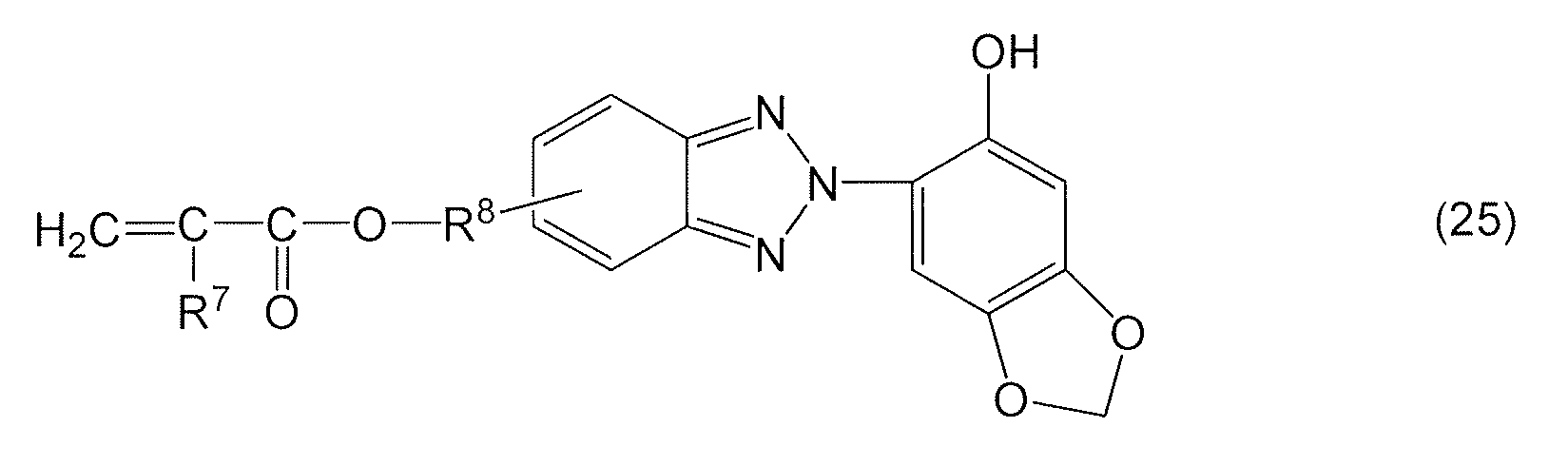
分光透過率調整剤は、光学フィルムの分光透過率を調整するものである。ハードコート層12に、例えば、下記一般式(21)で表されるセサモール型ベンゾトリアゾール系単量体を含ませた場合には、上述した分光透過率を好適に満たすことができる。
<Spectral transmittance adjuster>
The spectral transmittance adjuster adjusts the spectral transmittance of the optical film. For example, when the
式中、R7は水素原子又はメチル基を表す。R8は炭素数1~6の直鎖状又は枝分かれ鎖状のアルキレン基又は炭素数1~6の直鎖状または分岐鎖状のオキシアルキレン基を表す。 In the formula, R7 represents a hydrogen atom or a methyl group, and R8 represents a linear or branched alkylene group having 1 to 6 carbon atoms or a linear or branched oxyalkylene group having 1 to 6 carbon atoms.
上記のセサモール型ベンゾトリアゾール系単量体としては特に制限されないが、具体的な物質名としては、2-[2-(6-ヒドロキシベンゾ[1,3]ジオキソール-5-イル)-2H-ベンゾトリアゾール-5-イル]エチルメタクリレート、2-[2-(6-ヒドロキシベンゾ[1,3]ジオキソール-5-イル)-2H-ベンゾトリアゾール-5-イル]エチルアクリレート、3-[2-(6-ヒドロキシベンゾ[1,3]ジオキソール-5-イル)-2H-ベンゾトリアゾール-5-イル]プロピルメタクリレート、3-[2-(6-ヒドロキシベンゾ[1,3]ジオキソール-5-イル)-2H-ベンゾトリアゾール-5-イル]プロピルアクリレート、4-[2-(6-ヒドロキシベンゾ[1,3]ジオキソール-5-イル)-2H-ベンゾトリアゾール-5-イル]ブチルメタクリレート、4-[2-(6-ヒドロキシベンゾ[1,3]ジオキソール-5-イル)-2H-ベンゾトリアゾール-5-イル]ブチルアクリレート、2-[2-(6-ヒドロキシベンゾ[1,3]ジオキソール-5-イル)-2H-ベンゾトリアゾール-5-イルオキシ]エチルメタクリレート、2-[2-(6-ヒドロキシベンゾ[1,3]ジオキソール-5-イル)-2H-ベンゾトリアゾール-5-イルオキシ]エチルアクリレート、2-[3-{2-(6-ヒドロキシベンゾ[1,3]ジオキソール-5-イル)-2H-ベンゾトリアゾール-5-イル}プロパノイルオキシ]エチルメタクリレート、2-[3-{2-(6-ヒドロキシベンゾ[1,3]ジオキソール-5-イル)-2H-ベンゾトリアゾール-5-イル}プロパノイルオキシ]エチルアクリレート、4-[3-{2-(6-ヒドロキシベンゾ[1,3]ジオキソール-5-イル)-2H-ベンゾトリアゾール-5-イル}プロパノイルオキシ]ブチルメタクリレート、4-[3-{ 2 -(6-ヒドロキシベンゾ[1,3]ジオキソール-5-イル)-2H-ベンゾトリアゾール-5-イル}プロパノイルオキシ]ブチルアクリレート、2-[3-{2-(6-ヒドロキシベンゾ[1,3]ジオキソール-5-イル)-2H-ベンゾトリアゾール-5-イル}プロパノイルオキシ]エチルメタクリレート、2-[3-{2-(6-ヒドロキシベンゾ[1,3]ジオキソール-5-イル)-2H-ベンゾトリアゾール-5-イル}プロパノイルオキシ]エチルアクリレート、2-(メタクリロイルオキシ)エチル2-(6-ヒドロキシベンゾ[1,3]ジオキソール-5-イル)-2H-ベンゾトリアゾール-5カルボキシレート、2-(アクリロイルオキシ)エチル2-(6-ヒドロキシベンゾ[1,3]ジオキソール-5-イル)-2H-ベンゾトリアゾール-5-カルボキシレート、4-(メタクリロイルオキシ)ブチル2-(6-ヒドロキシベンゾ[1,3]ジオキソール-5-イル)-2H-ベンゾトリアゾール-5-カルボキシレート、4-(アクリロイルオキシ)ブチル2-(6-ヒドロキシベンゾ[1,3]ジオキソール-5-イル)-2H-ベンゾトリアゾール-5-カルボキシレート等を挙げることができる。また、これらセサモール型ベンゾトリアゾール系単量体は1種類で用いてもよいし、また2種類以上用いてもよい。 The sesamol-type benzotriazole monomer is not particularly limited, but specific substance names include 2-[2-(6-hydroxybenzo[1,3]dioxol-5-yl)-2H-benzotriazol-5-yl]ethyl methacrylate, 2-[2-(6-hydroxybenzo[1,3]dioxol-5-yl)-2H-benzotriazol-5-yl]ethyl acrylate, 3-[2-(6-hydroxybenzo[1,3]dioxol-5-yl)-2H-benzotriazol-5-yl]propyl methacrylate, 3-[2-(6-hydroxybenzo[1,3]dioxol-5-yl)-2H-benzotriazol-5-yl]propyl acrylate, 4-[2-(6-hydroxybenzo[1,3]dioxol-5-yl)-2H-benzotriazol-5-yl]butyl meth ...ethyl acrylate, 3-[2-(6-hydroxybenzo[1,3]dioxol-5-yl)-2H-benzotriazol-5-yl]propyl acrylate, 4-[2-(6-hydroxybenzo[1,3]dioxol-5-yl)-2H-benzotriazol-5-yl]butyl methacrylate, 4-[2-(6-hydroxybenzo[1,3]dioxol-5-yl]butyl methacrylate, 4-[2-(6-hydroxybenzo[1,3]dioxol-5-yl]ethyl acrylate, 3-[2-(6-hydroxybenzo[1,3]di 2-[2-(6-hydroxybenzo[1,3]dioxol-5-yl)-2H-benzotriazol-5-yloxy]ethyl acrylate, 2-[2-(6-hydroxybenzo[1,3]dioxol-5-yl)-2H-benzotriazol-5-yloxy]ethyl acrylate, 2-[3-{2-(6-hydroxybenzo[1,3]dioxol-5-yl)-2H-benzotriazol-5-yloxy]ethyl acrylate )-2H-benzotriazol-5-yl}propanoyloxy]ethyl methacrylate, 2-[3-{2-(6-hydroxybenzo[1,3]dioxol-5-yl)-2H-benzotriazol-5-yl}propanoyloxy]ethyl acrylate, 4-[3-{2-(6-hydroxybenzo[1,3]dioxol-5-yl)-2H-benzotriazol-5-yl}propanoyloxy]butyl methacrylate, 4-[3-{2-(6-hydroxybenzo[1,3]dioxol-5-yl)-2H-benzotriazol-5-yl}propanoyloxy]butyl methacrylate, -(6-hydroxybenzo[1,3]dioxol-5-yl)-2H-benzotriazol-5-yl}propanoyloxy]butyl acrylate, 2-[3-{2-(6-hydroxybenzo[1,3]dioxol-5-yl)-2H-benzotriazol-5-yl}propanoyloxy]ethyl methacrylate, 2-[3-{2-(6-hydroxybenzo[1,3]dioxol-5-yl)-2H-benzotriazol-5-yl}propanoyloxy]ethyl acrylate, 2-(methacryloyloxy)ethyl 2-(6-hydroxybenzo[1,3]dioxol-5-yl)-2H-benzotriazol-5-yl}propanoyloxy Examples of the sesamol-type benzotriazole monomer include 2-(acryloyloxy)ethyl 2-(6-hydroxybenzo[1,3]dioxol-5-yl)-2H-benzotriazole-5-carboxylate, 2-(acryloyloxy)ethyl 2-(6-hydroxybenzo[1,3]dioxol-5-yl)-2H-benzotriazole-5-carboxylate, 4-(methacryloyloxy)butyl 2-(6-hydroxybenzo[1,3]dioxol-5-yl)-2H-benzotriazole-5-carboxylate, 4-(acryloyloxy)butyl 2-(6-hydroxybenzo[1,3]dioxol-5-yl)-2H-benzotriazole-5-carboxylate, etc. Furthermore, these sesamol-type benzotriazole monomers may be used alone or in combination of two or more.
上記セサモール型ベンゾトリアゾール系単量体がハードコート層12に含有されている場合、例えば、上記セサモール型ベンゾトリアゾール系単量体は、ハードコート層12中15~30質量%で含有されていることが好ましい。このような範囲でセサモール型ベンゾトリアゾール系単量体が含有されていることで、上述した分光透過率を満たすことができる。なお、上記セサモール型ベンゾトリアゾール系単量体は、ハードコート層12において、ハードコート層12を構成する樹脂成分と反応して一体的に含有されていてもよく、ハードコート層12を構成する樹脂成分と反応することなく単独で含有されていてもよい。When the sesamol-type benzotriazole monomer is contained in the
<<無機層>>
無機層13は、主として無機物からなる層であり、例えば、無機層中に無機物が、55質量%以上存在していれば、無機層に該当する。無機層13は、有機成分を含んでいてもよいが、無機物のみから構成されていることが好ましい。ハードコート層12に接触している層が、無機層に該当するか否かは、X線光電子分光分析法(X-Ray Photoelectron Spectroscopy:XPSまたはElectron Spectroscopy for Chemical Analysis:ESCA)によって確認することができる。
<<Inorganic Layer>>
The
無機層13の構成材料としては、Ti、Al、Mg、Zr等の金属、または酸化ケイ素(SiOx(x=1~2))、酸化アルミニウム、酸化窒化ケイ素、酸化窒化アルミニウム、酸化マグネシウム、酸化亜鉛、酸化インジウム、酸化スズ、酸化イットリウム等の無機酸化物、無機窒化物、ダイヤモンドライクカーボン等が挙げられる。それらの中でも、透過率向上や耐擦傷性向上の観点から、酸化ケイ素が好ましい。
Examples of materials constituting the
無機層13は、ケイ素を含むことが好ましい。無機層13が、ケイ素を含むことにより、低屈折率化を図ることができる。無機層にケイ素が含まれるか否かは、X線光電子分光分析法(X-Ray Photoelectron Spectroscopy:XPSまたはElectron Spectroscopy for Chemical Analysis:ESCA)によって確認することができる。It is preferable that the
無機層13の膜厚は、10nm以上300nm以下となっていることが好ましい。無機層13の膜厚が、10nm以上であれば、優れた耐擦傷性を付与することができ、また300nm以下であれば、屈曲性や光学特性に影響なく他の層との密着性が良好である。無機層13の膜厚の下限は、30nm以上、50nm以上、80nm以上の順にさらに好ましく(数値が大きいほど好ましい)、上限は250nm以下、200nm以下、150nm以下の順にさらに好ましい(数値が小さいほど好ましい)。無機層13の膜厚は、ハードコート層12の膜厚と同様の方法によって求めるものとする。The thickness of the
無機層13においては、40°、相対湿度90%における水蒸気透過率(WVTR:Water Vapor Transmission Rate)が100g/(m2・24h)以下となっていることが好ましい。折り耐性は、温度が高く、また相対湿度が高いほど、悪化する。これは、無機層13が水分を透過し、透過した水分によってハードコート層が加水分解を起こすからであると考えられる。無機層13の上記水蒸気透過率が100g/(m2・24h)以下となっていることにより、無機層13を透過する水分を減らすことができるので、ハードコート層の加水分解を抑制することができる。水蒸気透過率はJIS K7129:2008に準拠した手法で得られる数値である。水蒸気透過率は、水蒸気透過率測定装置(製品名「PERMATRAN-W3/31」、MOCON社製)を用いて測定することができる。水蒸気透過率は、3回測定して得られた値の平均値とする。
In the
無機層13は、例えば、PVD法やCVD法等の蒸着法等を用いて形成することができる。PVD法としては、例えば、真空蒸着法、スパッタリング法、イオンプレーティング法等が挙げられる。真空蒸着法としては、例えば、エレクトロンビーム(EB)加熱方式による真空蒸着法、または、高周波誘電加熱方式による真空蒸着法等が挙げられる。The
<<機能層>>
機能層14は、光学フィルム10において、何らかの機能を発揮する層であり、機能層14としては、例えば、光学調整層、帯電防止層等が挙げられる。なお、機能層14が発揮する機能は、2以上であってもよい。例えば、機能層14は、光学調整機能と帯電防止機能の両方の機能を発揮する層であってもよい。
<<Functional layer>>
The
機能層14の膜厚は、30nm以上200nm以下となっていることが好ましい。機能層14の膜厚が、30nm以上であれば、ハードコート層12と光学調整層14の充分な密着性を確保でき、また200nm以下であれば、干渉縞をより抑制することができる。機能層14の下限は50nm以上、70nm以上、90nm以上の順にさらに好ましく(数値が大きいほど好ましい)、上限は150nm以下、140nm以下、130nm以下の順にさらに好ましい(数値が小さいほど好ましい)。機能層14の膜厚は、ハードコート層12の膜厚と同様の方法によって求めるものとする。The thickness of the
<光学調整層>
一般的に曲げられる光透過性基材を構成する樹脂は屈折率が高いので、光透過性基材とハードコート層の屈折率差が大きくなる。このため、光透過性基材とハードコート層との屈折率差に起因して、虹色状のムラである干渉縞が発生するおそれがある。光学調整層は、干渉縞の発生を抑制するための層である。光学調整層の屈折率は、干渉縞の発生を抑制する観点から、光透過性基材11の屈折率よりも低く、かつハードコート層12の屈折率よりも高いことが好ましい。光学調整層の屈折率は、例えば、ベッケ法によって測定することができる。光学調整層の屈折率を、ベッケ法を用いて測定する場合、光学調整層の欠片を10個切り出し、切り出した10個の欠片において、屈折率標準液を用いて、ベッケ法により屈折率をそれぞれ測定し、測定した欠片の屈折率の10個の平均値を光学調整層の屈折率とする。光透過性基材11やハードコート層12の屈折率も光学調整層の屈折率と同様の方法によって測定することができる。
<Optical Adjustment Layer>
Generally, the resin constituting the light-transmitting substrate that is bent has a high refractive index, so the refractive index difference between the light-transmitting substrate and the hard coat layer becomes large. Therefore, due to the refractive index difference between the light-transmitting substrate and the hard coat layer, there is a risk of occurrence of interference fringes, which are rainbow-like unevenness. The optical adjustment layer is a layer for suppressing the occurrence of interference fringes. From the viewpoint of suppressing the occurrence of interference fringes, the refractive index of the optical adjustment layer is preferably lower than that of the light-transmitting
光学調整層とハードコート層12との屈折率差(光学調整層の屈折率-ハードコート層の屈折率)は、0.005以上0.100以下であることが好ましい。この屈折率差が、0.005以上であれば、光学調整層とハードコート層12における界面反射は生じるが干渉縞が視認できないレベルにすることができ、また0.100以下であれば、干渉縞は若干確認されるが、実使用上問題ないレベルにすることができる。この屈折率差の下限は、0.007以上であることがより好ましく、上限は0.090以下であることがより好ましい。光学調整層の屈折率は、0.010以上0.080以下であってもよい。The refractive index difference between the optical adjustment layer and the hard coat layer 12 (refractive index of the optical adjustment layer - refractive index of the hard coat layer) is preferably 0.005 or more and 0.100 or less. If this refractive index difference is 0.005 or more, interfacial reflection occurs between the optical adjustment layer and the
光学調整層は、樹脂のみから構成されていてもよいが、バインダ樹脂および屈折率を調整するための粒子を含んでいることが好ましい。また、光学調整機能の他、帯電防止機能も発揮させるために、光学調整層は、帯電防止剤をさらに含んでいてもよい。光学調整層のバインダ樹脂は、(メタ)アクリル系樹脂、セルロース系樹脂、ウレタン系樹脂、塩化ビニル系樹脂、ポリエステル系樹脂、ポリオレフィン系樹脂、ポリカーボネート、ナイロン、ポリスチレン、およびABS樹脂からなる群より選択される少なくとも1種の樹脂であることが好ましい。光学調整層14の粒子は、シリカやフッ化マグネシウム等の低屈折率粒子、酸化チタンや酸化ジルコニウム等の金属酸化物粒子、コバルトブルー等の無機顔料等からなる群より選択される少なくとも1種であることが好ましい。これらの中でも、密着性と屈折率差調整の観点から、ポリエステル系樹脂と、酸化チタンや酸化ジルコニウム等の金属酸化物粒子との組み合わせがより好ましい。The optical adjustment layer may be composed of only resin, but preferably contains a binder resin and particles for adjusting the refractive index. In addition to the optical adjustment function, the optical adjustment layer may further contain an antistatic agent in order to exert an antistatic function. The binder resin of the optical adjustment layer is preferably at least one resin selected from the group consisting of (meth)acrylic resin, cellulose resin, urethane resin, vinyl chloride resin, polyester resin, polyolefin resin, polycarbonate, nylon, polystyrene, and ABS resin. The particles of the
<帯電防止層>
帯電防止層は、帯電防止剤を含んでいる。帯電防止剤としては、イオン伝導型帯電防止剤と電子伝導型帯電防止剤があり、バインダ樹脂との相溶性の観点から、イオン伝導型帯電防止剤が好ましい。
<Antistatic Layer>
The antistatic layer contains an antistatic agent. The antistatic agent may be an ion-conductive antistatic agent or an electron-conductive antistatic agent, and the ion-conductive antistatic agent is preferred from the viewpoint of compatibility with the binder resin.
上記イオン伝導型帯電防止剤としては、例えば、第4級アンモニウム塩、ピリジウム塩等のカチオン性帯電防止剤、スルホン酸、リン酸、カルボン酸等のアルカリ金属塩(例えば、リチウム塩、ナトリウム塩、カリウム塩等)等のアニオン性帯電防止剤、アミノ酸系、アミノ酸硫酸エステル系等の両性帯電防止剤、アミノアルコール系、グリセリン系、ポリエチレングリコール系等のノニオン性帯電防止剤等が挙げられる。これらの中でも、バインダ樹脂に対して優れた相溶性を示すことから、第4級アンモニウム塩やリチウム塩が好ましい。Examples of the ion-conducting antistatic agents include cationic antistatic agents such as quaternary ammonium salts and pyridinium salts, anionic antistatic agents such as alkali metal salts of sulfonic acid, phosphoric acid, carboxylic acid, etc. (e.g. lithium salts, sodium salts, potassium salts, etc.), amphoteric antistatic agents such as amino acid-based and amino acid sulfate-based, and nonionic antistatic agents such as amino alcohol-based, glycerin-based, and polyethylene glycol-based. Among these, quaternary ammonium salts and lithium salts are preferred because they have excellent compatibility with the binder resin.
上記電子伝導型帯電防止剤としては、例えば、ポリアセチレン系、ポリチオフェン系等の導電性ポリマー、金属粒子、金属酸化物粒子等の導電性粒子が挙げられる。これらの中でも、ポリアセチレン、ポリチオフェン等の導電性ポリマーにドーパントを組み合わせた帯電防止剤、金属粒子、金属酸化物粒子が好ましい。また、上記導電性ポリマーに導電性粒子を含有させることもできる。Examples of the electronically conductive antistatic agent include conductive polymers such as polyacetylene and polythiophene, metal particles, and conductive particles such as metal oxide particles. Among these, antistatic agents in which a dopant is combined with a conductive polymer such as polyacetylene or polythiophene, metal particles, and metal oxide particles are preferred. Conductive particles can also be incorporated into the conductive polymer.
上記導電性ポリマーからなる帯電防止剤としては、具体的には、ポリアセチレン、ポリアニリン、ポリチオフェン、ポリピロール、ポリフェニレンサルファイド、ポリ(1,6-ヘプタジイン)、ポリビフェニレン(ポリパラフェニレン)、ポリパラフィニレンスルフィド、ポリフェニルアセチレン、ポリ(2,5-チエニレン)、又は、これらの誘導体等の導電性高分子が挙げられ、好ましくは、ポリチオフェン系の導電性有機ポリマー(例えば、3,4-エチレンジオキシチオフェン(PEDOT)等)が挙げられる。 Specific examples of antistatic agents made of the above-mentioned conductive polymers include conductive polymers such as polyacetylene, polyaniline, polythiophene, polypyrrole, polyphenylene sulfide, poly(1,6-heptadiyne), polybiphenylene (polyparaphenylene), polyparaphenylene sulfide, polyphenylacetylene, poly(2,5-thienylene), or derivatives thereof, and preferably include polythiophene-based conductive organic polymers (e.g., 3,4-ethylenedioxythiophene (PEDOT)).
上記導電性有機ポリマーからなる帯電防止剤を用いることで、湿度依存性が少なく長期間にわたって帯電防止性が維持でき、また、高い透明性、低ヘイズ値を実現し、更に、高いハードコート性、特に鉛筆硬度、スチールウール等に対する耐擦傷性を著しく向上できる。By using an antistatic agent made of the above-mentioned conductive organic polymer, antistatic properties can be maintained for a long period of time with little humidity dependency, high transparency and low haze value can be achieved, and high hard coat properties, particularly pencil hardness and scratch resistance to steel wool, can be significantly improved.
上記金属粒子を構成する金属としては特に限定されず、例えば、Au、Ag、Cu、Al、Fe、Ni、Pd、Pt等の単独、あるいはこれら金属の合金が挙げられる。また、上記金属酸化物粒子を構成する金属酸化物としては特に限定されず、例えば、酸化錫(SnO2)、酸化アンチモン(Sb2O5)、アンチモンドープ酸化スズ(ATO)、スズドープ酸化インジウム(ITO)、アルミニウムドープ酸化亜鉛(AZO)、フッ素ドープ酸化スズ(FTO)、酸化亜鉛(ZnO)等が挙げられる。 The metal constituting the metal particles is not particularly limited, and examples thereof include Au, Ag, Cu, Al, Fe, Ni, Pd, Pt, etc., alone or alloys of these metals. The metal oxide constituting the metal oxide particles is not particularly limited, and examples thereof include tin oxide (SnO 2 ), antimony oxide (Sb 2 O 5 ), antimony-doped tin oxide (ATO), tin-doped indium oxide (ITO), aluminum-doped zinc oxide (AZO), fluorine-doped tin oxide (FTO), zinc oxide (ZnO), etc.
帯電防止剤の含有量としては、特に限定されないが、帯電防止層用組成物の重合性化合物100質量部に対して1質量部以上50質量部以下であることが好ましい。1質量部以上であれば、上述した帯電防止性を充分に得ることができ、50質量部以下であればヘイズ値が小さく、全光線透過率が良好な高透明の膜を得ることができる。上記帯電防止剤の含有量の下限は、10質量部以上であることがより好ましく、上限は40質量部以下であることがより好ましい。The content of the antistatic agent is not particularly limited, but is preferably 1 part by mass or more and 50 parts by mass or less per 100 parts by mass of the polymerizable compound of the antistatic layer composition. If it is 1 part by mass or more, the above-mentioned antistatic properties can be sufficiently obtained, and if it is 50 parts by mass or less, a highly transparent film with a small haze value and good total light transmittance can be obtained. The lower limit of the content of the antistatic agent is more preferably 10 parts by mass or more, and the upper limit is more preferably 40 parts by mass or less.
<<光学フィルムの製造方法>>
光学フィルム10は、例えば、以下のようにして作製することができる。まず、光透過性基材11の一方の面上に、バーコーター等の塗布装置によって、機能層14を形成するための機能層用組成物を塗布して、機能層用組成物の塗膜を形成する。なお、ここでの機能層用組成物は、光学調整層用組成物となっているが、帯電防止層用組成物であってもよい。
<<Method of Manufacturing Optical Film>>
The
<機能層用組成物>
機能層用組成物は、バインダ樹脂前駆体、金属酸化物等の粒子および溶剤を含んでいる。機能層用組成物は、その他、必要に応じて、シリカやフッ化マグネシウム等の低屈折率粒子、コバルトブルー等の無機顔料、レベリング剤、および重合開始剤の少なくともいずれかを含んでいてもよい。また、バインダ樹脂前駆体として、ポリエステル系樹脂を用いた場合には、機能層用組成物は、その他、必要に応じて、(メタ)アクリル系樹脂、セルロース系樹脂、ウレタン系樹脂、塩化ビニル系樹脂、ポリオレフィン系樹脂、ポリカーボネート、ナイロン、ポリスチレン、ABS樹脂からなる群より選択される1種以上の樹脂を含んでいてもよい。
<Composition for Functional Layer>
The functional layer composition contains a binder resin precursor, particles such as metal oxides, and a solvent. The functional layer composition may also contain at least one of low refractive index particles such as silica and magnesium fluoride, inorganic pigments such as cobalt blue, a leveling agent, and a polymerization initiator, as necessary. In addition, when a polyester resin is used as the binder resin precursor, the functional layer composition may also contain one or more resins selected from the group consisting of (meth)acrylic resins, cellulose resins, urethane resins, vinyl chloride resins, polyolefin resins, polycarbonates, nylons, polystyrenes, and ABS resins, as necessary.
機能層用組成物の塗膜を形成した後、各種の公知の方法で塗膜を、例えば40℃以上200℃以下の温度で10秒間~120秒間加熱することにより乾燥させ、溶剤を蒸発させて、または硬化させて、また必要に応じて塗膜に紫外線等の電離放射線を照射して、機能層14を形成する。After forming a coating film of the functional layer composition, the coating film is dried by various known methods, for example by heating at a temperature of 40°C or higher and 200°C or lower for 10 to 120 seconds, to evaporate the solvent or harden the coating film, and if necessary, the coating film is irradiated with ionizing radiation such as ultraviolet light to form the
機能層14を形成した後、機能層14上に、バーコーター等の塗布装置によって、ハードコート層12を形成するためのハードコート層用組成物を塗布して、ハードコート層用組成物の塗膜を形成する。After forming the
<ハードコート層用組成物>
ハードコート層用組成物は、硬化後にバインダ樹脂12Aとなる重合性化合物および無機粒子12Bを含んでいる。ハードコート層用組成物は、その他、必要に応じて、紫外線吸収剤、分光透過率調整剤、レベリング剤、溶剤、重合開始剤を含んでいてもよい。
<Hard Coat Layer Composition>
The composition for the hard coat layer contains a polymerizable compound that becomes a
(溶媒)
上記溶媒としては、アルコール(例、メタノール、エタノール、プロパノール、イソプロパノール、n-ブタノール、s-ブタノール、t-ブタノール、ベンジルアルコール、PGME、エチレングリコール、ジアセトンアルコール)、ケトン(例、アセトン、メチルエチルケトン、メチルイソブチルケトン、シクロペンタノン、シクロヘキサノン、ヘプタノン、ジイソブチルケトン、ジエチルケトン、ジアセトンアルコール)、エステル(酢酸メチル、酢酸エチル、酢酸ブチル、酢酸n-プロピル、酢酸イソプロピル、蟻酸メチル、PGMEA)、脂肪族炭化水素(例、ヘキサン、シクロヘキサン)、ハロゲン化炭化水素(例、メチレンクロライド、クロロホルム、四塩化炭素)、芳香族炭化水素(例、ベンゼン、トルエン、キシレン)、アミド(例、ジメチルホルムアミド、ジメチルアセトアミド、n-メチルピロリドン)、エーテル(例、ジエチルエーテル、ジオキサン、テトラヒドロフラン)、エーテルアルコール(例、1-メトキシ-2-プロパノール)、カーボネート(炭酸ジメチル、炭酸ジエチル、炭酸エチルメチル)、等が挙げられる。これらの溶媒、単独で用いられてもよく、2種類以上が併用されてもよい。なかでも、上記溶媒としては、ウレタン(メタ)アクリレート等の成分、並びに、他の添加剤を溶解或いは分散させ、上記樹脂層用組成物を好適に塗工できる点で、メチルイソブチルケトン、メチルエチルケトンが好ましい。
(solvent)
Examples of the solvent include alcohols (e.g., methanol, ethanol, propanol, isopropanol, n-butanol, s-butanol, t-butanol, benzyl alcohol, PGME, ethylene glycol, diacetone alcohol), ketones (e.g., acetone, methyl ethyl ketone, methyl isobutyl ketone, cyclopentanone, cyclohexanone, heptanone, diisobutyl ketone, diethyl ketone, diacetone alcohol), esters (methyl acetate, ethyl acetate, butyl acetate, n-propyl acetate, isopropyl acetate, methyl formate, PGMEA), aliphatic hydrocarbons (e.g., hexane, cyclohexane), halogenated hydrocarbons (e.g., methylene chloride, chloroform, carbon tetrachloride), aromatic hydrocarbons (e.g., benzene, toluene, xylene), amides (e.g., dimethylformamide, dimethylacetamide, n-methylpyrrolidone), ethers (e.g., diethyl ether, dioxane, tetrahydrofuran), ether alcohols (e.g., 1-methoxy-2-propanol), carbonates (dimethyl carbonate, diethyl carbonate, ethyl methyl carbonate), and the like. These solvents may be used alone or in combination of two or more. Among them, methyl isobutyl ketone and methyl ethyl ketone are preferred as the solvent, since they can dissolve or disperse components such as urethane (meth)acrylate and other additives and can suitably coat the resin layer composition.
(重合開始剤)
重合開始剤は、電離放射線照射または熱により分解されて、ラジカルを発生して重合性化合物の重合(架橋)を開始または進行させる成分である。
(Polymerization initiator)
The polymerization initiator is a component that is decomposed by irradiation with ionizing radiation or heat to generate radicals and initiate or advance polymerization (crosslinking) of a polymerizable compound.
重合開始剤は、電離放射線照射または熱によりラジカル重合を開始させる物質を放出することが可能であれば特に限定されない。重合開始剤としては、特に限定されず、公知のものを用いることができ、具体例には、例えば、アセトフェノン類、ベンゾフェノン類、ミヒラーベンゾイルベンゾエート、α-アミロキシムエステル、チオキサントン類、プロピオフェノン類、ベンジル類、ベンゾイン類、アシルホスフィンオキシド類が挙げられる。また、光増感剤を混合して用いることが好ましく、その具体例としては、例えば、n-ブチルアミン、トリエチルアミン、ポリ-n-ブチルホスフィン等が挙げられる。The polymerization initiator is not particularly limited as long as it is capable of releasing a substance that initiates radical polymerization by irradiation with ionizing radiation or heat. The polymerization initiator is not particularly limited, and known initiators can be used. Specific examples include acetophenones, benzophenones, Michler's benzoyl benzoate, α-amyloxime ester, thioxanthones, propiophenones, benzils, benzoins, and acylphosphine oxides. It is also preferable to use a mixture of photosensitizers. Specific examples include n-butylamine, triethylamine, and poly-n-butylphosphine.
ハードコート層用組成物の塗膜を形成した後、各種の公知の方法で塗膜を、例えば30℃以上120℃以下の温度で10秒間~120秒間加熱することにより乾燥させ、溶剤を蒸発させる。After forming a coating film of the hard coat layer composition, the coating film is dried by various known methods, for example by heating at a temperature of 30°C or higher and 120°C or lower for 10 to 120 seconds, to evaporate the solvent.
塗膜を乾燥させた後、塗膜に紫外線等の電離放射線を照射して、塗膜を硬化させて、ハードコート層12を形成する。After drying the coating film, the coating film is irradiated with ionizing radiation such as ultraviolet light to harden the coating film and form a
ハードコート層12を形成した後、例えば、スパッタリング法等の蒸着法によって、ハードコート層12に接するように無機層13を形成する。これにより、図1に示される光学フィルム10が得られる。After forming the
<<<画像表示装置>>>
光学フィルム10は、折り畳み可能な画像表示装置に組み込んで使用することが可能である。図4は、本実施形態に係る画像表示装置の概略構成図である。図4に示されるように、画像表示装置40は、観察者側に向けて、主に、電池等が収納された筐体41、保護フィルム42、表示パネル43、タッチセンサ44、円偏光板45、および光学フィルム10がこの順で積層されている。表示パネル43とタッチセンサ44との間、タッチセンサ44と円偏光板45との間、円偏光板45と光学フィルム10との間には、例えば、OCA(Optical Clear Adhesive)等の光透過性接着層46が配置されており、これら部材は光透過性接着層46によって互いに固定されている。
<<<Image display device>>>
The
光学フィルム10は、ハードコート層12が光透過性基材11よりも観察者側となるように配置されている。画像表示装置40においては、光学フィルム10の表面10Aが、画像表示装置40の表面40Aを構成している。The
画像表示装置40においては、表示パネル43は、有機発光ダイオード等を含む有機発光ダイオードパネルとなっている。タッチセンサ44は、円偏光板45よりも表示パネル43側に配置されているが、円偏光板45と光学フィルム10との間に配置されていてもよい。また、タッチセンサ44は、オンセル方式やインセル方式であってもよい。In the
本発明者らは、ハードコート層上に無機層が形成された光学フィルムの耐擦傷性に対して鋭意研究を重ねたところ、ハードコート層に無機粒子を含有させ、ハードコート層の膜厚を1μm以上とし、かつハードコート層のインデンテーション硬さを200MPa以上とすることによって、耐擦傷性を向上させることができることを見出した。これは、適当な無機粒子を適当なハードコート層に配合することで、無機層との密着性を確保し、かつハードコート層の高硬度化を達成できたためであると考えられる。本実施形態によれば、バインダ樹脂12Aおよび無機粒子12Bを含むハードコート層12の膜厚を1μm以上とし、かつハードコート層12のインデンテーション硬さを200MPa以上としているので、優れた耐擦傷性を有する光学フィルム10を提供することができる。The present inventors have conducted extensive research into the scratch resistance of optical films having an inorganic layer formed on a hard coat layer, and have found that scratch resistance can be improved by incorporating inorganic particles into the hard coat layer, setting the film thickness of the hard coat layer to 1 μm or more, and setting the indentation hardness of the hard coat layer to 200 MPa or more. This is believed to be because the incorporation of suitable inorganic particles into a suitable hard coat layer ensures adhesion to the inorganic layer and achieves high hardness of the hard coat layer. According to this embodiment, the film thickness of the
ハードコート層の表面に対してスチールウール試験を行うと、無機粒子は脱落しやすい。このため、耐擦傷性を向上させる観点からは、ハードコート層は無機粒子を含まないことが好ましいとも考えられるが、本実施形態においては、ハードコート層12上に無機層13が形成されているので、スチールウール試験時にハードコート層12中の無機粒子12Bが脱落することを抑制できる。これにより、無機粒子12を含有させることでハードコート層12の硬度を高めることができ、耐擦傷性を向上させることができる。When a steel wool test is performed on the surface of the hard coat layer, the inorganic particles are likely to fall off. For this reason, from the viewpoint of improving scratch resistance, it is considered preferable that the hard coat layer does not contain inorganic particles. However, in this embodiment, the
[第2の実施形態]
以下、本発明の第2の実施形態に係る光学フィルムおよび画像表示装置について、図面を参照しながら説明する。図5は本実施形態に係る光学フィルムの概略構成図である。なお、図5において、図1と同じ符号が付されている部材は、図1で示した部材と同じものであるので、説明を省略するものとする。
Second Embodiment
Hereinafter, an optical film and an image display device according to a second embodiment of the present invention will be described with reference to the drawings. Fig. 5 is a schematic diagram of the optical film according to this embodiment. In Fig. 5, the members having the same reference numerals as those in Fig. 1 are the same as those in Fig. 1, and therefore the description thereof will be omitted.
<<<光学フィルム>>>
図5に示される光学フィルム50は、光学フィルム10と同様に、光透過性基材11、ハードコート層51および無機層13をこの順で備えている。図5においては、光学フィルム50の表面50Aは、無機層13の表面13Aとなっており、裏面50Bは、光透過性基材11におけるハードコート層51側の面とは反対側の面となっている。光学フィルム50の物性は、光学フィルム10の物性と同様であるので、ここでは説明を省略するものとする。
<<<Optical films>>>
The
<<ハードコート層>>
ハードコート層51は、ハードコート層12の欄で説明した理由と同様の理由から、インデンテーション硬さが200MPa以上となっており、また膜厚も、1μm以上となっている。ハードコート層51のインデンテーション硬さおよび膜厚の好ましい上限、下限は、ハードコート層12のインデンテーション硬さおよび膜厚の好ましい上限、下限と同様になっている。なお、ハードコート層51のその他の物性等は、ハードコート層12の物性等と同様であるので、ここでは、説明を省略するものとする。
<<Hard Coat Layer>>
The
ハードコート層51は、金属元素および半金属元素の少なくともいずれかを含んでいる。ハードコート層51が、金属元素および半金属元素の少なくともいずれかを含むことにより、無機層13との密着性を向上させることができるので、耐擦傷性を向上させることができる。金属元素としては、例えば、アルミニウムや錫等の典型金属元素およびジルコニウムやチタン等の遷移金属元素のいずれであってもよい。また、半金属元素としては、例えば、ホウ素、ケイ素、ゲルマニウム、ヒ素、アンチモン及びテルル等が挙げられる。ハードコート層が上記元素を含んでいるか否かは、以下の方法によって確認することができる。まず、1mm×6mmの大きさに切り出した光学フィルムにおいて、面内に対し2°以下の角度でミクロトーム(製品名「ウルトラミクロトーム EM UC7」、ライカ マイクロシステムズ株式会社製)で無機層の膜厚以上に切削して、ハードコート層を露出させる。その後、X線光電子分光分析装置(ESCA、製品名「KRATOS Nova」、株式会社島津製作所製)を用いて、上記切削することによって得られた表面から元素分析を行う。これにより、ハードコート層が金属元素および半金属元素の少なくともいずれかを含んでいるか否か確認することができる。The
ハードコート層51に含まれ、かつX線光電子分光分析法により測定される金属元素および半金属元素の合計の原子比率は、1.5%以上30%以下であることが好ましい。上記金属元素および半金属元素の合計の原子比率が、1.5%以上であれば、無機層13との密着性をより向上させることができ、また、30%以下であれば、屈曲性を維持することができる。上記金属元素および半金属元素の合計の原子比率は、上記元素分析を行うために切削することによって得られた表面において、X線光電子分光分析装置(ESCA、製品名「KRATOS Nova」、株式会社島津製作所製)を用いて、測定するものとする。ハードコート層51中の上記金属元素および半金属元素の合計量の原子比率の下限は、2%以上、5%以上であることがより好ましく(数値が大きいほどが好ましい)、上限は、25%以下、20%以下であることがより好ましい(数値が小さいほど好ましい)。The total atomic ratio of the metal elements and metalloid elements contained in the
ハードコート層51は、耐擦傷性をより向上させる観点からシリコーン樹脂51Aおよび無機粒子51Bを含んでいることが好ましい。ただし、ハードコート層51が金属元素および半金属元素の少なくともいずれかを含んでいれば、シリコーン樹脂51Aおよび無機粒子51Bの両方を含まなくともよい。例えば、ハードコート層が、シリコーン樹脂を含む場合には、ハードコート層はシリコーン樹脂由来のケイ素を含むので、無機粒子51Bを含まなくともよい。また、ハードコート層が、無機粒子としてシリカ粒子を含む場合には、ハードコート層はシリカ粒子由来のケイ素を含むので、シリコーン樹脂を含まなくともよい。本明細書における「シリコーン樹脂」とは、シロキサン結合(ケイ素と酸素との結合)による主骨格を有する高分子化合物のことを意味する。ハードコート層51は、シリコーン樹脂51Aおよび無機粒子51Bの他、紫外線吸収剤、分光透過率調整剤のような添加剤を含んでいてもよい。From the viewpoint of further improving the scratch resistance, the
<シリコーン樹脂>
シリコーン樹脂51Aとしては、重合性官能基を有する一般式(R9SiO1.5)nで表されるシルセスキオキサンを含む重合性化合物の重合体(硬化物)であることが好ましい。上記式中、R9は、ラジカル重合性官能基やカチオン重合性官能基等の重合性官能基であり、nは1以上の整数である。重合性化合物は、上記シルセスキオキサンの他、他の重合性化合物を含んでいてもよいが、上記シルセスキオキサンのみであってもよい。シリコーン樹脂51Aが、このようなシルセスキオキサンを含む重合性化合物の重合体を含んでいることにより、無機層との密着性をより確保できる。ラジカル重合性官能基としては、例えば、(メタ)アクリロイル基、ビニル基、アリル基等のエチレン性不飽和基等が挙げられ、カチオン重合性官能基としては、例えば、エポキシ基やオキセタニル基等が挙げられる。このようなラジカル重合性官能基やカチオン重合性官能基を含ませることにより、シルセスキオキサン同士を連結することができ、重合体を得ることができる。
<Silicone resin>
The
シルセスキオキサンの構造としては、特に限定されず、例えば、完全籠型や不完全籠型等の籠型構造、はしご型構造、ランダム型構造等が挙げられるが、いずれの構造であってもよい。シルセスキオキサンの市販品としては、例えば、コンストゥールケミカル株式会社製のGlycidyl polysilsesquioxane cage mixtureや東亞合成株式会社製の光硬化型SQシリーズが挙げられる。The structure of the silsesquioxane is not particularly limited, and may be any of a complete cage structure, an incomplete cage structure, a ladder structure, a random structure, etc. Commercially available silsesquioxanes include, for example, Glycidyl polysilsesquioxane cage mixture manufactured by Constur Chemical Co., Ltd. and the photocurable SQ series manufactured by Toagosei Co., Ltd.
シリコーン樹脂51Aを形成する重合性化合物は、上記シルセスキオキサンの代わりに、(メタ)アクリロイル基等のラジカル重合性官能基を有するジメチルポリシロキサン、アルコキシシリル基を有するシリコーンオリゴマー、および/またはシリコーンポリマー等を含んでいてもよい。上記シリコーンオリゴマーやシリコーンポリマーは、ハードコート層の硬度をより高めることができる観点から、ラジカル重合性官能基またはカチオン重合性官能基等の重合性官能基を有することが好ましい。The polymerizable compound forming the
ラジカル重合性官能基を有するジメチルポリシロキサンの市販品としては、信越化学工業株式会社製のKRシリーズ、例えば、KP-410、KP-411、KP-412、KP-413、KP-414、KP-415、KP-423(いずれも両末端型)、KP-416、KP418、KP-422(いずれも片末端型)、KP-420(側鎖型)が挙げられる。Commercially available dimethylpolysiloxanes having radically polymerizable functional groups include the KR series manufactured by Shin-Etsu Chemical Co., Ltd., such as KP-410, KP-411, KP-412, KP-413, KP-414, KP-415, KP-423 (all both end types), KP-416, KP418, KP-422 (all one end type), and KP-420 (side chain type).
アルコキシシリル基を有するシリコーンオリゴマーの市販品としては、例えば、信越化学工業株式会社製のKR-500、KR-515、KC-895、X-40-9225等が挙げられる。また、超高分子シリコーン樹脂としては、例えば、信越化学工業株式会社製のKR-251等が挙げられる。Commercially available silicone oligomers having alkoxysilyl groups include, for example, KR-500, KR-515, KC-895, and X-40-9225 manufactured by Shin-Etsu Chemical Co., Ltd. Furthermore, examples of ultra-high molecular weight silicone resins include, for example, KR-251 manufactured by Shin-Etsu Chemical Co., Ltd.
<無機粒子>
無機粒子51Bは、第1実施形態で説明した無機粒子12Bと同様であるので、ここでは説明を省略するものとする。
<Inorganic particles>
The
本発明者らは、ハードコート層上に無機層が形成された光学フィルムの耐擦傷性に対して鋭意研究を重ねたところ、ハードコート層に金属元素および半金属元素の少なくともいずれかを含ませ、ハードコート層の膜厚を1μm以上とし、かつハードコート層のインデンテーション硬さを200MPa以上とすることによって、耐擦傷性を向上させることができることを見出した。これは、金属元素および半金属元素の少なくともいずれかをハードコート層に含ませることで、無機層との密着性を確保し、かつハードコート層の高硬度化を達成できたためであると考えられる。本実施形態によれば、金属元素および半金属元素の少なくともいずれかを含むハードコート層51の膜厚を1μm以上とし、かつハードコート層51のインデンテーション硬さを200MPa以上としているので、優れた耐擦傷性を有する光学フィルム50を提供することができる。The present inventors have conducted extensive research into the scratch resistance of an optical film having an inorganic layer formed on a hard coat layer, and have found that scratch resistance can be improved by including at least one of a metal element and a metalloid element in the hard coat layer, making the film thickness of the hard coat layer 1 μm or more, and making the indentation hardness of the hard coat layer 200 MPa or more. This is believed to be because the inclusion of at least one of a metal element and a metalloid element in the hard coat layer ensures adhesion to the inorganic layer and achieves high hardness of the hard coat layer. According to this embodiment, the film thickness of the
ハードコート層の表面に対してスチールウール試験を行うと、無機粒子は脱落しやすい。このため、耐擦傷性を向上させる観点からは、ハードコート層は無機粒子を含まないことが好ましいとも考えられるが、本実施形態においては、ハードコート層51上に無機層13が形成されているので、スチールウール試験時にハードコート層51中の無機粒子51Bが脱落することを抑制できる。これにより、無機粒子51Bを含有させることでハードコート層51の硬度を高めることができ、耐擦傷性を向上させることができる。When a steel wool test is performed on the surface of the hard coat layer, the inorganic particles are likely to fall off. For this reason, from the viewpoint of improving scratch resistance, it is considered preferable that the hard coat layer does not contain inorganic particles. However, in this embodiment, the
<<<画像表示装置>>>
光学フィルム50は、折り畳み可能な画像表示装置に組み込んで使用することが可能である。図6は、本実施形態に係る画像表示装置の概略構成図である。図6に示される画像表示装置60は、光学フィルム50を備えている。画像表示装置60は、光学フィルム10を光学フィルム50としたこと以外は、画像表示装置40と同様であるので、ここでは説明を省略するものとする。
<<<Image display device>>>
The
本発明を詳細に説明するために、以下に実施例を挙げて説明するが、本発明はこれらの記載に限定されない。なお、下記の「固形分100%換算値」とは、溶剤希釈品中の固形分を100%としたときの値である。In order to explain the present invention in detail, the following examples are given, but the present invention is not limited to these examples. Note that the "100% solids equivalent value" below is the value when the solids content in the solvent-diluted product is 100%.
<ハードコート層用組成物の調製>
まず、下記に示す組成となるように各成分を配合して、光学調整層用組成物を得た。
(ハードコート層用組成物1)
・ポリエステルアクリレート(製品名「M-9050」、東亞合成株式会社製):50質量部
・シリカ粒子(製品名「MIBK-SD」、日産化学工業株式会社製):50質量部
・重合開始剤(1-ヒドロキシシクロヘキシルフェニルケトン、製品名「Irgacure(登録商標)184」、BASFジャパン社製):5質量部
・メチルイソブチルケトン:100質量部
<Preparation of hard coat layer composition>
First, the components were mixed so as to obtain the composition shown below, thereby obtaining a composition for an optical adjustment layer.
(Hardcoat layer composition 1)
Polyester acrylate (product name "M-9050", manufactured by Toagosei Co., Ltd.): 50 parts by mass Silica particles (product name "MIBK-SD", manufactured by Nissan Chemical Industries, Ltd.): 50 parts by mass Polymerization initiator (1-hydroxycyclohexyl phenyl ketone, product name "Irgacure (registered trademark) 184", manufactured by BASF Japan): 5 parts by mass Methyl isobutyl ketone: 100 parts by mass
(ハードコート層用組成物2)
・ポリエステルアクリレート(製品名「M-9050」、東亞合成株式会社製):67質量部
・シリカ粒子(製品名「MIBK-SD」、日産化学工業株式会社製):33質量部
・重合開始剤(1-ヒドロキシシクロヘキシルフェニルケトン、製品名「Irgacure(登録商標)184」、BASFジャパン社製):5質量部
・メチルイソブチルケトン:100質量部
(Hardcoat layer composition 2)
Polyester acrylate (product name "M-9050", manufactured by Toagosei Co., Ltd.): 67 parts by mass Silica particles (product name "MIBK-SD", manufactured by Nissan Chemical Industries, Ltd.): 33 parts by mass Polymerization initiator (1-hydroxycyclohexyl phenyl ketone, product name "Irgacure (registered trademark) 184", manufactured by BASF Japan): 5 parts by mass Methyl isobutyl ketone: 100 parts by mass
(ハードコート層用組成物3)
・ポリエステルアクリレート(製品名「M-9050」、東亞合成株式会社製):90質量部
・シリカ粒子(製品名「MIBK-SD」、日産化学工業株式会社製):10質量部
・重合開始剤(1-ヒドロキシシクロヘキシルフェニルケトン、製品名「Irgacure(登録商標)184」、BASFジャパン社製):5質量部
・メチルイソブチルケトン:100質量部
(Hardcoat layer composition 3)
Polyester acrylate (product name "M-9050", manufactured by Toagosei Co., Ltd.): 90 parts by mass Silica particles (product name "MIBK-SD", manufactured by Nissan Chemical Industries, Ltd.): 10 parts by mass Polymerization initiator (1-hydroxycyclohexyl phenyl ketone, product name "Irgacure (registered trademark) 184", manufactured by BASF Japan Ltd.): 5 parts by mass Methyl isobutyl ketone: 100 parts by mass
(ハードコート層用組成物4)
・アルコキシ化ジペンタエリスリトールアクリレート(製品名「A-DPH-12E」、新中村化学工業株式会社製):50質量部
・シリカ粒子(製品名「MIBK-SD」、日産化学工業株式会社製):50質量部
・重合開始剤(1-ヒドロキシシクロヘキシルフェニルケトン、製品名「Irgacure(登録商標)184」、BASFジャパン社製):5質量部
・メチルイソブチルケトン:100質量部
(Hardcoat layer composition 4)
Alkoxylated dipentaerythritol acrylate (product name "A-DPH-12E", manufactured by Shin-Nakamura Chemical Co., Ltd.): 50 parts by mass; Silica particles (product name "MIBK-SD", manufactured by Nissan Chemical Industries, Ltd.): 50 parts by mass; Polymerization initiator (1-hydroxycyclohexyl phenyl ketone, product name "Irgacure (registered trademark) 184", manufactured by BASF Japan): 5 parts by mass; Methyl isobutyl ketone: 100 parts by mass
(ハードコート層用組成物5)
・グリシジルポリシルセスキオキサン(製品名「Glycidyl polysilsesquioxane cage mixture」、コンストゥールケミカル株式会社製):100質量部
・重合開始剤(トリ-p-トリルスルホニウムヘキサフルオロホスファート、東京化成工業株式会社製):5質量部
・1-メトキシ-2-プロパノール:100質量部
(Hardcoat layer composition 5)
Glycidyl polysilsesquioxane (product name "Glycidyl polysilsesquioxane cage mixture", manufactured by Constell Chemical Co., Ltd.): 100 parts by mass Polymerization initiator (tri-p-tolylsulfonium hexafluorophosphate, manufactured by Tokyo Chemical Industry Co., Ltd.): 5 parts by mass 1-Methoxy-2-propanol: 100 parts by mass
(ハードコート層用組成物6)
・ポリエステルアクリレート(製品名「M-9050」、東亞合成株式会社製):100質量部
・重合開始剤(1-ヒドロキシシクロヘキシルフェニルケトン、製品名「Irgacure(登録商標)184」、BASFジャパン社製):5質量部
・メチルイソブチルケトン:100質量部
(Hardcoat layer composition 6)
Polyester acrylate (product name "M-9050", manufactured by Toagosei Co., Ltd.): 100 parts by mass Polymerization initiator (1-hydroxycyclohexyl phenyl ketone, product name "Irgacure (registered trademark) 184", manufactured by BASF Japan Ltd.): 5 parts by mass Methyl isobutyl ketone: 100 parts by mass
(ハードコート層用組成物7)
・ポリプロピレングリコールジアクリレート(製品名「M-220」、東亞合成株式会社製):90質量部
・シリカ粒子(製品名「MIBK-SD」、日産化学工業株式会社製):10質量部
・重合開始剤(1-ヒドロキシシクロヘキシルフェニルケトン、製品名「Irgacure(登録商標)184」、BASFジャパン社製):5質量部
・メチルイソブチルケトン:100質量部
(Hardcoat layer composition 7)
Polypropylene glycol diacrylate (product name "M-220", manufactured by Toagosei Co., Ltd.): 90 parts by mass Silica particles (product name "MIBK-SD", manufactured by Nissan Chemical Industries, Ltd.): 10 parts by mass Polymerization initiator (1-hydroxycyclohexyl phenyl ketone, product name "Irgacure (registered trademark) 184", manufactured by BASF Japan Ltd.): 5 parts by mass Methyl isobutyl ketone: 100 parts by mass
<光学調整層用組成物の調製>
下記に示す組成となるように各成分を配合して、光学調整層用組成物を得た。
(光学調整層用組成物1)
・ウレタン変性ポリエステル系樹脂(製品名「UR-3200」、東洋紡株式会社製):85質量部(固形分100%換算値)
・酸化ジルコニウム(平均粒子径20nm、CIKナノテック株式会社製):15質量部(固形分100%換算値)
・メチルイソブチルケトン(MIBK):170質量部
<Preparation of composition for optical adjustment layer>
The components were mixed so as to obtain the composition shown below, thereby obtaining a composition for an optical adjustment layer.
(Composition 1 for optical adjustment layer)
Urethane-modified polyester resin (product name "UR-3200", manufactured by Toyobo Co., Ltd.): 85 parts by mass (based on 100% solids)
Zirconium oxide (
Methyl isobutyl ketone (MIBK): 170 parts by mass
<ポリイミド系基材の作製>
500mlのセパラブルフラスコに、脱水されたジメチルアセトアミド278.0gおよび1,3-ビス(3-アミノプロピル)テトラメチルジシロキサン(AprTMOS)8.1g(33mmol)を溶解させた溶液を液温30℃に制御し、そこへ、4,4’-(ヘキサフルオロイソプロピリデン)ジフタル酸無水物(6FDA)18.1g(41mmol)を、温度上昇が2℃以下になるように徐々に投入し、メカニカルスターラーで1時間撹拌した。そこへ、2,2’-ビス(トリフルオロメチル)ベンジジン(TFMB)46.1g(131mmol)を添加し、完全に溶解したことを確認後、4,4’-(ヘキサフルオロイソプロピリデン)ジフタル酸無水物(6FDA)51.8g(122mmol)を温度上昇が2℃以下になるように数回に分けて徐々に投入し、ポリイミド前駆体1が溶解したポリイミド前駆体溶液(1)(固形分30重量%)を合成した。
<Preparation of polyimide substrate>
A solution of 278.0 g of dehydrated dimethylacetamide and 8.1 g (33 mmol) of 1,3-bis(3-aminopropyl)tetramethyldisiloxane (AprTMOS) dissolved in a 500 ml separable flask was controlled to a liquid temperature of 30° C., and 18.1 g (41 mmol) of 4,4'-(hexafluoroisopropylidene)diphthalic anhydride (6FDA) was gradually added thereto so that the temperature rise was not more than 2° C., and the solution was stirred with a mechanical stirrer for 1 hour. To the solution, 46.1 g (131 mmol) of 2,2'-bis(trifluoromethyl)benzidine (TFMB) was added, and after confirming that it was completely dissolved, 51.8 g (122 mmol) of 4,4'-(hexafluoroisopropylidene)diphthalic anhydride (6FDA) was gradually added in several portions so that the temperature rise was 2°C or less, thereby synthesizing a polyimide precursor solution (1) (solid content 30 wt%) in which polyimide precursor 1 was dissolved.
上記ポリイミド前駆体溶液(1)を室温まで下げ、脱水されたジメチルアセトアミドを196.8g加え均一になるまで撹拌した。次に触媒であるピリジン128.9g(1.63mol)と無水酢酸167.7g(1.63mol)を加え24時間室温で撹拌し、ポリイミド溶液を合成した。得られたポリイミド溶液400.0gを5Lのセパラブルフラスコに移し、酢酸ブチル119.2gを加え均一になるまで撹拌した。次にメタノール688.0gを徐々に加え、僅かに濁りが見られる溶液を得た。濁りのみられる溶液にメタノール2.064kgを一気に加え白色スラリーを得た。上記スラリーをろ過し、5回メタノールで洗浄し、ポリイミド樹脂(1)を65.0g得た。The polyimide precursor solution (1) was cooled to room temperature, and 196.8 g of dehydrated dimethylacetamide was added and stirred until homogenous. Next, 128.9 g (1.63 mol) of pyridine and 167.7 g (1.63 mol) of acetic anhydride, which were catalysts, were added and stirred at room temperature for 24 hours to synthesize a polyimide solution. 400.0 g of the resulting polyimide solution was transferred to a 5 L separable flask, and 119.2 g of butyl acetate was added and stirred until homogenous. Next, 688.0 g of methanol was gradually added to obtain a slightly turbid solution. 2.064 kg of methanol was added at once to the turbid solution to obtain a white slurry. The above slurry was filtered and washed five times with methanol to obtain 65.0 g of polyimide resin (1).
酢酸ブチル42.2gに上記ポリイミド樹脂(1)を10.0g加え、室温で1時間撹拌しポリイミド溶液を得た。ポリイミド溶液は卓上型超音波洗浄機(製品名「UT-104」、シャープ株式会社製)で10分間脱気し、取り出した後、室温で1時間静置させた。静置させたポリイミド溶液を厚み250μmのポリエチレンテレフタレート(PET)フィルム(製品名「ルミラーT60」、東レ株式会社製)上に塗布し、40℃の循環オーブンで10分間、150℃で10分間乾燥させた後、PETフィルムから剥離し、さらに150℃で1時間乾燥させ、大きさA5サイズ(148mm×210mm)および厚さ50μmのポリイミド系基材を得た。なお、ポリイミド系基材の厚みは、走査型電子顕微鏡(SEM)を用いて、ポリイミド系基材の断面を撮影し、その断面の画像においてポリイミド系基材の厚みを10箇所測定し、その10箇所の膜厚の算術平均値とした。10.0 g of the polyimide resin (1) was added to 42.2 g of butyl acetate and stirred at room temperature for 1 hour to obtain a polyimide solution. The polyimide solution was degassed for 10 minutes using a tabletop ultrasonic cleaner (product name "UT-104", manufactured by Sharp Corporation), removed, and allowed to stand at room temperature for 1 hour. The polyimide solution that had been left to stand was applied to a 250 μm thick polyethylene terephthalate (PET) film (product name "Lumirror T60", manufactured by Toray Industries, Inc.), dried for 10 minutes in a 40°C circulation oven and for 10 minutes at 150°C, then peeled off from the PET film and further dried at 150°C for 1 hour to obtain a polyimide-based substrate of A5 size (148 mm x 210 mm) and 50 μm thick. The thickness of the polyimide-based substrate was measured by photographing a cross section of the polyimide-based substrate using a scanning electron microscope (SEM), measuring the thickness of the polyimide-based substrate at 10 points on the image of the cross section, and calculating the arithmetic average value of the film thicknesses at the 10 points.
<実施例1>
光透過性基材として、屈折率1.630および厚さ50μmのポリイミド系基材(製品名「ネオプリム」、三菱ガス化学株式会社製)を準備し、ポリイミド系基材の一方の面に、バーコーターでハードコート層用組成物1を塗布し、塗膜を形成した。その後、形成した塗膜に対して、70℃、1分間加熱させることにより塗膜中の溶剤を蒸発させ、紫外線照射装置(フュージョンUVシステムジャパン株式会社製、光源Hバルブ)を用いて、紫外線を窒素雰囲気中にて積算光量が200mJ/cm2になるように照射して塗膜を硬化させて、屈折率1.521および膜厚4μmのハードコート層を形成した。最後に、ハードコート層の表面に、スパッタリング法により膜厚100nmのSiOx(x=1~2未満)からなる無機層を形成し、光学フィルムを得た。
Example 1
A polyimide-based substrate (product name "Neoplum", manufactured by Mitsubishi Gas Chemical Co., Ltd.) with a refractive index of 1.630 and a thickness of 50 μm was prepared as a light-transmitting substrate, and a hard coat layer composition 1 was applied to one side of the polyimide-based substrate with a bar coater to form a coating film. The formed coating film was then heated at 70° C. for 1 minute to evaporate the solvent in the coating film, and an ultraviolet irradiation device (manufactured by Fusion UV Systems Japan Co., Ltd., light source H bulb) was used to irradiate ultraviolet light in a nitrogen atmosphere to an integrated light amount of 200 mJ/cm 2 to harden the coating film, forming a hard coat layer with a refractive index of 1.521 and a thickness of 4 μm. Finally, an inorganic layer made of SiO x (x=1 to less than 2) with a thickness of 100 nm was formed on the surface of the hard coat layer by a sputtering method to obtain an optical film.
上記ポリイミド系基材の厚みは、走査型電子顕微鏡(SEM)を用いて、ポリイミド系基材の断面を撮影し、その断面の画像においてポリイミド系基材の厚みをそれぞれ10箇所測定し、その10箇所の厚みの算術平均値とした。また、ハードコート層の膜厚は、走査透過型電子顕微鏡(STEM)(製品名「S-4800」、株式会社日立ハイテクノロジーズ製)を用いて、ハードコート層の断面を撮影し、その断面の画像においてハードコート層の膜厚を10箇所測定し、その10箇所の膜厚の算術平均値とした。ハードコート層の断面写真は、以下のようにして撮影した。まず、1mm×10mmに切り出した光学フィルムを包埋樹脂によって包埋したブロックを作製し、このブロックから一般的な切片作製方法によって穴等がない均一な、厚さ70nm以上100nm以下の切片を切り出した。切片の作製には、「ウルトラミクロトーム EM UC7」(ライカ マイクロシステムズ株式会社)等を用いた。そして、この穴等がない均一な切片を測定サンプルとした。その後、走査透過型電子顕微鏡(STEM)を用いて、測定サンプルの断面写真を撮影した。この断面写真の撮影の際には、検出器を「TE」、加速電圧を「30kV」、エミッション電流を「10μA」にしてSTEM観察を行った。倍率については、フォーカスを調節しコントラストおよび明るさを各層が見分けられるか観察しながら5000倍~20万倍で適宜調節した。なお、断面写真の撮影の際には、さらに、アパーチャーを「ビームモニタ絞り3」にし、対物レンズ絞りを「3」にし、またW.D.を「8mm」にした。無機層の膜厚も、ハードコート層の膜厚と同様の方法によって測定した。また、ポリイミド系基材等およびハードコート層の屈折率は、JIS K7142:2008のB法に準拠したベッケ法によって求めた。ポリイミド系基材の屈折率を、ベッケ法を用いて求める場合、ポリイミド系基材の欠片を10個切り出し、切り出した10個の欠片において、波長589nmのナトリウムD線および屈折率標準液を用いて、欠片の屈折率をそれぞれ測定し、測定した欠片の屈折率の10個の平均値をポリイミド系基材の屈折率とした。ハードコート層の屈折率を、ベッケ法を用いて求める場合も、上記ベッケ法によるポリイミド系基材の屈折率の求め方と同様の方法によって求めた。実施例2~7および比較例1~4においても、実施例1と同様の手法によってポリイミド系基材等の厚みおよび屈折率を測定した。The thickness of the polyimide-based substrate was measured by photographing the cross section of the polyimide-based substrate using a scanning electron microscope (SEM), measuring the thickness of the polyimide-based substrate at 10 points on the image of the cross section, and taking the arithmetic average value of the thicknesses at the 10 points. The thickness of the hard coat layer was measured by photographing the cross section of the hard coat layer using a scanning transmission electron microscope (STEM) (product name "S-4800", manufactured by Hitachi High-Technologies Corporation), measuring the thickness of the hard coat layer at 10 points on the image of the cross section, and taking the arithmetic average value of the thicknesses at the 10 points. The cross-sectional photograph of the hard coat layer was taken as follows. First, a block was prepared by embedding an optical film cut to 1 mm x 10 mm in embedding resin, and a uniform slice with a thickness of 70 nm to 100 nm without holes was cut from this block using a general slice preparation method. An "Ultramicrotome EM UC7" (Leica Microsystems Inc.) or the like was used to prepare the slices. The uniform slice without holes was used as the measurement sample. Then, a scanning transmission electron microscope (STEM) was used to take a cross-sectional photograph of the measurement sample. When taking this cross-sectional photograph, the detector was set to "TE", the acceleration voltage was set to "30 kV", and the emission current was set to "10 μA" to perform STEM observation. The magnification was appropriately adjusted from 5,000 to 200,000 times while adjusting the focus and observing whether the contrast and brightness of each layer could be distinguished. In addition, when taking the cross-sectional photograph, the aperture was set to "beam monitor aperture 3", the objective lens aperture was set to "3", and the WD was set to "8 mm". The thickness of the inorganic layer was also measured by the same method as the thickness of the hard coat layer. In addition, the refractive index of the polyimide-based substrate and the hard coat layer was determined by the Becke method in accordance with the B method of JIS K7142:2008. When the refractive index of the polyimide-based substrate is determined using the Becke method, 10 pieces of the polyimide-based substrate are cut out, and the refractive index of each of the cut pieces is measured using a sodium D line having a wavelength of 589 nm and a refractive index standard solution, and the average value of the refractive index of the measured pieces is taken as the refractive index of the polyimide-based substrate. When the refractive index of the hard coat layer is determined using the Becke method, it is determined in the same manner as the refractive index of the polyimide-based substrate by the Becke method. In Examples 2 to 7 and Comparative Examples 1 to 4, the thickness and refractive index of the polyimide-based substrate, etc. are measured in the same manner as in Example 1.
<実施例2>
実施例2においては、ハードコート層用組成物1の代わりにハードコート層用組成物2を用いたこと以外は、実施例1と同様にして、光学フィルムを得た。
Example 2
In Example 2, an optical film was obtained in the same manner as in Example 1, except that the composition 2 for a hard coat layer was used instead of the composition 1 for a hard coat layer.
<実施例3>
実施例3においては、ハードコート層用組成物1の代わりにハードコート層用組成物3を用いたこと以外は、実施例1と同様にして、光学フィルムを得た。
Example 3
In Example 3, an optical film was obtained in the same manner as in Example 1, except that the composition 3 for a hard coat layer was used instead of the composition 1 for a hard coat layer.
<実施例4>
実施例4においては、ハードコート層用組成物1の代わりにハードコート層用組成物4を用いたこと以外は、実施例1と同様にして、光学フィルムを得た。
Example 4
In Example 4, an optical film was obtained in the same manner as in Example 1, except that the composition 4 for a hard coat layer was used instead of the composition 1 for a hard coat layer.
<実施例5>
実施例5においては、ハードコート層の膜厚を2μmにしたこと以外は、実施例1と同様にして、光学フィルムを得た。
Example 5
In Example 5, an optical film was obtained in the same manner as in Example 1, except that the thickness of the hard coat layer was changed to 2 μm.
<実施例6>
実施例6においては、ハードコート層の膜厚を10μmにしたこと以外は、実施例1と同様にして、光学フィルムを得た。
Example 6
In Example 6, an optical film was obtained in the same manner as in Example 1, except that the thickness of the hard coat layer was 10 μm.
<実施例7>
実施例7においては、ハードコート層の膜厚を20μmにしたこと以外は、実施例1と同様にして、光学フィルムを得た。
Example 7
In Example 7, an optical film was obtained in the same manner as in Example 1, except that the thickness of the hard coat layer was 20 μm.
<実施例8>
光透過性基材として、屈折率1.630および厚さ50μmのポリイミド系基材(製品名「ネオプリム」、三菱ガス化学株式会社製)を準備し、ポリイミド系基材の一方の面に、バーコーターで光学調整層用組成物1を塗布し、塗膜を形成した。その後、形成した塗膜に対して、90℃で1分間加熱させることにより塗膜中の溶剤を蒸発させて、屈折率1.562および膜厚100nmの光学調整層を形成した。光学調整層を形成した後、光学調整層の表面に、バーコーターでハードコート層用組成物1を塗布し、塗膜を形成した。その後、形成した塗膜に対して、70℃、1分間加熱させることにより塗膜中の溶剤を蒸発させ、紫外線照射装置(フュージョンUVシステムジャパン株式会社製、光源Hバルブ)を用いて、紫外線を窒素雰囲気中にて積算光量が200mJ/cm2になるように照射して塗膜を硬化させて、屈折率1.521および膜厚4μmのハードコート層を形成した。最後に、ハードコート層の表面に、スパッタリング法により膜厚100nmのSiOx(x=1~2未満)からなる無機層を形成し、光学フィルムを得た。光学調整層の膜厚も、走査透過型電子顕微鏡(STEM)(製品名「S-4800」、株式会社日立ハイテクノロジーズ製)を用いて、光学調整層の断面を撮影し、その断面の画像において光学調整層の厚みをそれぞれ10箇所測定し、その10箇所の厚みの算術平均値とした。光学調整層の膜厚は、ハードコート層の膜厚と同様の方法によって測定した。また光学調整層の屈折率は、ポリイミド系基材等と同様にJIS K7142:2008のB法に準拠したベッケ法によって求めた。
Example 8
As a light-transmitting substrate, a polyimide substrate (product name "Neoplum", manufactured by Mitsubishi Gas Chemical Co., Ltd.) having a refractive index of 1.630 and a thickness of 50 μm was prepared, and a composition for optical adjustment layer 1 was applied to one side of the polyimide substrate with a bar coater to form a coating film. The formed coating film was then heated at 90 ° C. for 1 minute to evaporate the solvent in the coating film, forming an optical adjustment layer having a refractive index of 1.562 and a thickness of 100 nm. After forming the optical adjustment layer, a composition for hard coat layer 1 was applied to the surface of the optical adjustment layer with a bar coater to form a coating film. The formed coating film was then heated at 70 ° C. for 1 minute to evaporate the solvent in the coating film, and an ultraviolet irradiation device (manufactured by Fusion UV System Japan Co., Ltd., light source H bulb) was used to irradiate ultraviolet light in a nitrogen atmosphere to an integrated light amount of 200 mJ / cm 2 to harden the coating film, forming a hard coat layer having a refractive index of 1.521 and a thickness of 4 μm. Finally, an inorganic layer of SiO x (x=1 to less than 2) having a thickness of 100 nm was formed on the surface of the hard coat layer by a sputtering method to obtain an optical film. The thickness of the optical adjustment layer was also measured by photographing a cross section of the optical adjustment layer using a scanning transmission electron microscope (STEM) (product name "S-4800", manufactured by Hitachi High-Technologies Corporation), measuring the thickness of the optical adjustment layer at 10 points on the cross section image, and taking the arithmetic average value of the thicknesses at the 10 points. The thickness of the optical adjustment layer was measured by the same method as the thickness of the hard coat layer. The refractive index of the optical adjustment layer was also measured by the Becke method in accordance with JIS K7142:2008 B method, similar to the polyimide-based substrate.
<実施例9>
実施例9においては、ポリイミド系基材(製品名「ネオプリム」、三菱ガス化学株式会社製)を上記で作製したポリイミド系基材1を用いたこと以外は、実施例1と同様にして、光学フィルムを得た。
<Example 9>
In Example 9, an optical film was obtained in the same manner as in Example 1, except that the polyimide-based substrate 1 prepared above was used as the polyimide-based substrate (product name: "Neoprim", manufactured by Mitsubishi Gas Chemical Company, Inc.).
<実施例10>
実施例10においては、ハードコート層用組成物1の代わりにハードコート層用組成物5を用いたこと以外は、実施例1と同様にして、光学フィルムを得た。
Example 10
In Example 10, an optical film was obtained in the same manner as in Example 1, except that the composition 5 for a hard coat layer was used instead of the composition 1 for a hard coat layer.
<比較例1>
比較例1においては、ハードコート層用組成物1の代わりにハードコート層用組成物6を用いたこと以外は、実施例1と同様にして、光学フィルムを得た。
<Comparative Example 1>
In Comparative Example 1, an optical film was obtained in the same manner as in Example 1, except that Composition 6 for a hard coat layer was used instead of Composition 1 for a hard coat layer.
<比較例2>
比較例2においては、ハードコート層用組成物1の代わりにハードコート層用組成物7を用いたこと以外は、実施例1と同様にして、光学フィルムを得た。
<Comparative Example 2>
In Comparative Example 2, an optical film was obtained in the same manner as in Example 1, except that Composition 7 for a hard coat layer was used instead of Composition 1 for a hard coat layer.
<比較例3>
比較例3においては、ハードコート層の膜厚を0.8μmにしたこと以外は、実施例1と同様にして、光学フィルムを得た。
<Comparative Example 3>
In Comparative Example 3, an optical film was obtained in the same manner as in Example 1, except that the thickness of the hard coat layer was 0.8 μm.
<インデンテーション硬さ測定>
実施例および比較例に係る光学フィルムのハードコート層のインデンテーション硬さを測定した。具体的には、まず1mm×10mmに切り出した光学フィルムを包埋樹脂によって包埋したブロックを作製し、このブロックから一般的な切片作製方法によって穴等がない均一な、厚さ70nm以上100nm以下の切片を切り出した。切片の作製には、「ウルトラミクロトーム EM UC7」(ライカ マイクロシステムズ株式会社)を用いた。そして、この穴等がない均一な切片が切り出された残りのブロックを測定サンプルとした。次いで、このような測定サンプルにおける上記切片が切り出されることによって得られた断面において、圧子としてバーコビッチ(Berkovich)圧子(三角錐、BRUKER社製のTI-0039)を、以下の測定条件で、ハードコート層の断面に25秒間かけて最大押し込み荷重500μNとなるまで垂直に押し込んだ。ここで、バーコビッチ圧子は、実施例1~7、9、10および比較例1~3に係る光学フィルムにおいては、ポリイミド系基材や無機層の影響を避けるためおよびハードコート層の側縁の影響を避けるために、ポリイミド系基材とハードコート層の界面からハードコート層の中央側に500nm離れ、ハードコート層と無機層の界面からハードコート層の中央側に500nm離れ、ハードコート層の両側端からそれぞれハードコート層の中央側に500nm離れたハードコート層の部分内に押し込んだ。また、同様の理由から、実施例8に係る光学フィルムにおいては、光学調整層とハードコート層の界面からハードコート層の中央側に500nm離れ、ハードコート層と無機層の界面からハードコート層の中央側に500nm離れ、ハードコート層の両側端からそれぞれハードコート層の中央側に500nm離れたハードコート層の部分内に押し込んだ。その後、一定時間保持して残留応力の緩和を行った後、25秒かけて除荷し、緩和後の最大荷重を計測し、該最大荷重Pmax(μN)と接触投影面積Ap(nm2)とを用い、Pmax/Apにより、インデンテーション硬さを算出した。上記接触投影面積は、標準試料の溶融石英(BRUKER社製の5-0098)を用いてOliver-Pharr法で圧子先端曲率を補正した接触投影面積であった。インデンテーション硬さ(HIT)は、10箇所測定して得られた値の算術平均値とした。なお、測定値の中に算術平均値から±20%以上外れるものが含まれている場合は、その測定値を除外し再測定を行うものとする。
(測定条件)
・荷重速度:20μN/秒
・保持時間:5秒
・荷重除荷速度:20μN/秒
・測定温度:25℃
<Indentation hardness measurement>
The indentation hardness of the hard coat layer of the optical film according to the examples and comparative examples was measured. Specifically, first, a block was prepared by embedding an optical film cut to 1 mm x 10 mm in an embedding resin, and a uniform slice having a thickness of 70 nm to 100 nm without holes was cut out from this block by a general slice preparation method. An "Ultramicrotome EM UC7" (Leica Microsystems, Inc.) was used to prepare the slices. The remaining block from which the uniform slice without holes was cut out was used as a measurement sample. Next, a Berkovich indenter (triangular pyramid, TI-0039 manufactured by BRUKER) was pressed vertically into the cross section of the hard coat layer under the following measurement conditions for 25 seconds until the maximum pressing load reached 500 μN. Here, in the optical films according to Examples 1 to 7, 9, and 10 and Comparative Examples 1 to 3, in order to avoid the influence of the polyimide-based substrate and the inorganic layer and to avoid the influence of the side edges of the hard coat layer, the Berkovich indenter was pressed into a portion of the hard coat layer that was 500 nm away from the interface between the polyimide-based substrate and the hard coat layer toward the center of the hard coat layer, 500 nm away from the interface between the hard coat layer and the inorganic layer toward the center of the hard coat layer, and 500 nm away from each of both ends of the hard coat layer toward the center of the hard coat layer. Also, for the same reason, in the optical film according to Example 8, the Berkovich indenter was pressed into a portion of the hard coat layer that was 500 nm away from the interface between the optical adjustment layer and the hard coat layer toward the center of the hard coat layer, 500 nm away from the interface between the hard coat layer and the inorganic layer toward the center of the hard coat layer, and 500 nm away from each of both ends of the hard coat layer toward the center of the hard coat layer. After that, the specimen was held for a certain time to relax the residual stress, and then unloaded over 25 seconds. The maximum load after relaxation was measured, and the indentation hardness was calculated by P max /A p using the maximum load P max (μN) and the contact projected area A p (nm 2 ). The contact projected area was the contact projected area corrected for the indenter tip curvature by the Oliver-Pharr method using a standard sample of fused quartz (5-0098 manufactured by BRUKER). The indentation hardness (H IT ) was the arithmetic average value of the values obtained by measuring at 10 points. If the measured values include any that deviate from the arithmetic average value by ±20% or more, the measured values are excluded and remeasured.
(Measurement conditions)
・Loading speed: 20μN/sec ・Holding time: 5 seconds ・Unloading speed: 20μN/sec ・Measurement temperature: 25℃
<金属元素および半金属元素の存在確認およびこれらの元素の合計量の原子比率測定>
実施例および比較例に係る光学フィルムのハードコート層に金属元素および半金属元素の少なくともいずれかが存在するか否か確認した。具体的には、まず、1mm×6mmの大きさに切り出した光学フィルムにおいて、面内に対し平行方向にミクロトーム(製品名「ウルトラミクロトーム EM UC7」、ライカ マイクロシステムズ株式会社製)で200nm程度切削して、ハードコート層を露出させた。その後、X線光電子分光分析装置(ESCA、製品名「KRATOS Nova」、株式会社島津製作所製)を用いて、上記切削することによって得られた表面において元素分析を行い、金属元素および半金属元素の少なくともいずれかを含んでいるか否か確認した。また、その際、上記切削することによって得られた表面において、X線光電子分光分析装置(ESCA、製品名「KRATOS Nova」、株式会社島津製作所製)を用いて金属元素および半金属元素の合計量の原子比率(%)を測定した。
(測定条件)
・測定手法:Wide・Narrow
・X線源:モノクロAlKα
・X線出力:150W
・エミッション電流:10mA
・加速電圧:15kV
・帯電中和機構:ON
・測定領域:300×700μm
・Pass Energy(Survey):160eV
・Pass Energy(Narrow):40eV
<Confirmation of the presence of metallic elements and semi-metallic elements and measurement of the atomic ratio of the total amount of these elements>
It was confirmed whether or not at least one of metal elements and metalloid elements was present in the hard coat layer of the optical film according to the examples and comparative examples. Specifically, first, the optical film cut into a size of 1 mm x 6 mm was cut by about 200 nm in a direction parallel to the in-plane direction with a microtome (product name "Ultramicrotome EM UC7", manufactured by Leica Microsystems, Inc.) to expose the hard coat layer. Then, an elemental analysis was performed on the surface obtained by the above cutting using an X-ray photoelectron spectroscopy analyzer (ESCA, product name "KRATOS Nova", manufactured by Shimadzu Corporation) to confirm whether or not at least one of metal elements and metalloid elements was contained. In addition, the atomic ratio (%) of the total amount of metal elements and metalloid elements was measured on the surface obtained by the above cutting using an X-ray photoelectron spectroscopy analyzer (ESCA, product name "KRATOS Nova", manufactured by Shimadzu Corporation).
(Measurement conditions)
Measurement method: Wide/Narrow
X-ray source: Monochrome AlKα
・X-ray output: 150W
Emission current: 10mA
Acceleration voltage: 15 kV
Charge neutralization mechanism: ON
・Measurement area: 300 x 700μm
・Pass Energy (Survey): 160eV
・Pass Energy (Narrow): 40eV
<シリカ粒子の面積比率>
実施例および比較例に係る光学フィルムのハードコート層の膜厚方向の断面において、ハードコート層と無機層の界面からハードコート層の深さ500nmまでの界面近傍領域における無機粒子の面積比率を求めた。上記界面近傍領域における無機粒子の面積比率は、以下のようにして求めた。まず、1mm×10mmに切り出した光学フィルムを包埋樹脂によって包埋したブロックを作製し、このブロックから一般的な切片作製方法によって穴等がない均一な、厚さ70nm以上100nm以下の切片10枚を切り出した。切片の作製には、「ウルトラミクロトーム EM UC7」(ライカ マイクロシステムズ株式会社)を用いた。そして、この穴等がない均一な切片10枚を測定サンプルとした。次いで、走査透過型電子顕微鏡(STEM)(製品名「S-4800」、株式会社日立ハイテクノロジーズ製)により各測定サンプルの断面写真を撮影した。なお、測定サンプル1枚につき1箇所の断面写真を撮影するものとした。この断面写真の撮影の際には、検出器を「TE」、加速電圧を「30kV」、エミッション電流を「10μA」にして観察を行った。倍率については、フォーカスを調節しコントラストおよび明るさを各層が見分けられるか観察しながら5000倍~20万倍で適宜調節した。なお、断面写真の撮影の際には、さらに、アパーチャーを「ビームモニタ絞り3」にし、対物レンズ絞りを「3」にし、またW.D.を「8mm」にした。そして、得られた10枚の断面写真において、界面近傍領域の面積を100%とし、界面近傍領域の面積に占める無機粒子の面積の比率(面積比率)を求めた。上記界面近傍領域における無機粒子の面積比率は、上記界面近傍領域の10枚の断面写真から求めた無機粒子の面積比率の算術平均値とした。
<Area ratio of silica particles>
In the cross section in the thickness direction of the hard coat layer of the optical film according to the examples and comparative examples, the area ratio of inorganic particles in the interface vicinity region from the interface between the hard coat layer and the inorganic layer to a depth of 500 nm in the hard coat layer was obtained. The area ratio of inorganic particles in the interface vicinity region was obtained as follows. First, a block was prepared by embedding an optical film cut to 1 mm x 10 mm in embedding resin, and 10 uniform slices with a thickness of 70 nm to 100 nm were cut out from this block by a general slice preparation method. An "Ultramicrotome EM UC7" (Leica Microsystems, Inc.) was used to prepare the slices. The 10 uniform slices without holes were used as measurement samples. Next, a cross-sectional photograph of each measurement sample was taken using a scanning transmission electron microscope (STEM) (product name "S-4800", manufactured by Hitachi High-Technologies Corporation). It was decided that a cross-sectional photograph was taken at one location per measurement sample. When taking the cross-sectional photograph, the detector was set to "TE", the acceleration voltage was set to "30 kV", and the emission current was set to "10 μA". The magnification was appropriately adjusted from 5,000 times to 200,000 times while observing whether the layers could be distinguished by adjusting the focus and observing whether the contrast and brightness could be distinguished. When taking the cross-sectional photograph, the aperture was set to "beam monitor aperture 3", the objective lens aperture was set to "3", and the WD was set to "8 mm". Then, in the obtained 10 cross-sectional photographs, the area of the interface vicinity region was set to 100%, and the ratio of the area of the inorganic particles to the area of the interface vicinity region (area ratio) was obtained. The area ratio of the inorganic particles in the interface vicinity region was taken as the arithmetic average value of the area ratio of the inorganic particles obtained from the 10 cross-sectional photographs of the interface vicinity region.
<耐擦傷性>
実施例および比較例に係る光学フィルムの表面(無機層の表面)に対して、スチールウール試験を行い、評価した。具体的には、50mm×100mmの大きさに切り出した光学フィルムをガラス板上に折れやシワがないようニチバン株式会社製のセロテープ(登録商標)で無機層が上側となるように固定した状態で、♯0000番のスチールウール(製品名「BON STAR」、日本スチールウール株式会社製)を用いて、1kg/cm2の荷重をかけながら、速度50mm/秒で10往復擦るスチールウール試験を行い、その後の光学フィルムの表面に傷の有無を目視により確認した。評価基準は、以下の通りとした。
○:傷や削れが確認されなかった、または傷や削れが若干確認されたが実用上問題がないレベルであった。
×:傷や削れが明らかに確認された。
<Scratch resistance>
The surface (surface of inorganic layer) of the optical film according to the embodiment and the comparative example was subjected to a steel wool test and evaluated.Specifically, the optical film cut into a size of 50 mm x 100 mm was fixed on a glass plate with the inorganic layer facing up using Cellophane Tape (registered trademark) manufactured by Nichiban Co., Ltd. so as not to bend or wrinkle, and the steel wool test was performed by rubbing 10 times back and forth at a speed of 50 mm/sec with a load of 1 kg/ cm2 using #0000 steel wool (product name "BON STAR", manufactured by Nippon Steel Wool Co., Ltd.), and then visually checking the presence or absence of scratches on the surface of the optical film.The evaluation criteria were as follows.
◯: No scratches or scrapes were found, or some scratches or scrapes were found but at a level that did not cause any practical problems.
×: Scratches or scratches were clearly observed.
<ヘイズ測定>
実施例および比較例に係る光学フィルムのヘイズ値(全ヘイズ値)をそれぞれ測定した。ヘイズ値は、ヘイズメーター(製品名「HM-150」、村上色彩技術研究所製)を用いてJIS K7136:2000に準拠した方法により測定した。上記ヘイズ値は、50mm×100mmの大きさに切り出した後、カールや皺がなく、かつ指紋や埃等がない状態で無機層側が非光源側となるように設置し、光学フィルム1枚に対して3回測定し、3回測定して得られた値の算術平均値とした。
<Haze measurement>
The haze value (total haze value) of the optical films according to the examples and comparative examples was measured. The haze value was measured by a method conforming to JIS K7136:2000 using a haze meter (product name "HM-150", manufactured by Murakami Color Research Laboratory). The haze value was measured three times for each optical film, after cutting out a piece having a size of 50 mm x 100 mm, with no curls or wrinkles and no fingerprints or dust, and placing the piece so that the inorganic layer side was on the non-light source side. The arithmetic average value of the values obtained by the three measurements was determined.
<全光線透過率>
実施例および比較例に係る光学フィルムの全光線透過率をそれぞれ測定した。全光線透過率は、ヘイズメーター(製品名「HM-150」、村上色彩技術研究所製)を用いてJIS K7361-1:1997に準拠した方法により測定した。上記全光線透過率は、上記全光線透過率は、50mm×100mmの大きさに切り出した後、カールや皺がなく、かつ指紋や埃等がない状態で無機層側が非光源側となるように設置し、光学フィルム1枚に対して3回測定し、3回測定して得られた値の算術平均値とした。
<Total light transmittance>
The total light transmittance of the optical films according to the examples and comparative examples was measured. The total light transmittance was measured by a method conforming to JIS K7361-1:1997 using a haze meter (product name "HM-150", manufactured by Murakami Color Research Laboratory). The total light transmittance was measured three times for each optical film, after cutting out a piece having a size of 50 mm x 100 mm, and placing the piece in a state free of curls, wrinkles, fingerprints, dust, etc., with the inorganic layer side facing the non-light source side, and the arithmetic average value of the values obtained by the three measurements was used.
<折り畳み性>
実施例および比較例に係る光学フィルムに対して折り畳み試験を行い、折り畳み性を評価した。具体的には、まず、30mm×100mmの大きさに切り出した光学フィルムを、耐久試験機(製品名「DLDMLH-FS」、ユアサシステム機器株式会社製)に、光学フィルムの短辺側を固定部でそれぞれ固定し、図3(C)に示したように対向する2つの辺部の最小の間隔が6mmとなるようにして取り付け、光学フィルムの表面側を180°となるように10万回折り畳む折り畳み試験(無機層が内側となり、ポリイミド系基材が外側となるように折り畳む試験)を行い、屈曲部に割れ又は破断が生じていないか調べた。また、同様に、30mm×100mmの大きさに切り出した新しい光学フィルムを、耐久試験機(製品名「DLDMLH-FS」、ユアサシステム機器株式会社製)に、光学フィルムの短辺側を固定部でそれぞれ固定し、対向する2つの辺部の最小の間隔が2mmとなるようにして取り付け、光学フィルムの表面側を180°となるように10万回折り畳む折り畳み試験(無機層が内側となり、ポリイミド系基材が外側となるように折り畳む試験)を行い、屈曲部に割れ又は破断が生じていないか調べた。評価基準は、以下の通りとした。
(折り畳み性)
○:折り畳み試験において、屈曲部に割れ又は破断が生じていなかった。
×:折り畳み試験において、屈曲部に割れ又は破断が生じていた。
<Foldability>
The optical films according to the examples and the comparative examples were subjected to a folding test to evaluate the foldability. Specifically, the optical film cut into a size of 30 mm x 100 mm was attached to a durability tester (product name "DLDMLH-FS", manufactured by Yuasa System Equipment Co., Ltd.) with the short sides of the optical film fixed at the fixing parts, and the short sides of the optical film were attached so that the minimum distance between the two opposing sides was 6 mm as shown in Fig. 3(C), and a folding test was performed in which the front side of the optical film was folded 100,000 times at 180° (a test in which the inorganic layer was folded on the inside and the polyimide-based base material was folded on the outside), and the bent parts were examined for cracks or breakage. Similarly, a new optical film cut to a size of 30 mm x 100 mm was attached to a durability tester (product name "DLDMLH-FS", manufactured by Yuasa System Devices Co., Ltd.) with the short sides of the optical film fixed at the fixing parts and the minimum distance between the two opposing sides being 2 mm, and a folding test was performed in which the front side of the optical film was folded 100,000 times at 180° (a test in which the film was folded so that the inorganic layer was on the inside and the polyimide-based base material was on the outside), and the bent parts were checked for cracks or breaks. The evaluation criteria were as follows:
(Foldability)
◯: No cracks or breaks were observed at the bent portion during the folding test.
×: Cracks or breaks occurred at the bent portion during the folding test.
<干渉縞評価>
実施例および比較例に係る光学フィルムにおいて、干渉縞が観察されるか評価した。具体的には、50mm×100mmの大きさに切り出した光学フィルムの裏面に厚み25μmの透明粘着剤(製品名「高透明性両面テープ 8146-1」、スリーエム社製)を介して、裏面反射を防止するための黒色アクリル板を貼り、光学フィルムの表面側から各光学フィルムに光を照射し、干渉縞が確認されるか目視で観察した。光源としては、三波長管蛍光灯を使用した。干渉縞の発生を以下の基準により評価した。
○:干渉縞は確認されなかった。
△:干渉縞は若干確認された。
×:干渉縞が明確に確認された。
<Interference fringe evaluation>
The optical films according to the examples and the comparative examples were evaluated for whether interference fringes were observed. Specifically, a black acrylic plate was attached to the back surface of an optical film cut into a size of 50 mm x 100 mm via a transparent adhesive having a thickness of 25 μm (product name: Highly transparent double-sided tape 8146-1, manufactured by 3M) to prevent back surface reflection, and light was irradiated onto each optical film from the front surface side of the optical film, and visual observation was made to see whether interference fringes were observed. A three-wavelength fluorescent lamp was used as the light source. The occurrence of interference fringes was evaluated according to the following criteria.
○: No interference fringes were observed.
△: Slight interference fringes were observed.
×: interference fringes were clearly observed.


以下、結果について述べる。表1に示されるように、比較例1に係る光学フィルムにおいては、ハードコート層が無機粒子または金属元素および半金属元素の少なくともいずれかを含んでいなかったので、無機層の表面における耐擦傷性が劣っていた。比較例2に係る光学フィルムは、インデンテーション硬さが200MPa未満であったので、無機層の表面における耐擦傷性が劣っていた。比較例3に係る光学フィルムは、ハードコート層の膜厚が小さかったので、無機層の表面における耐擦傷性が劣っていた。これに対し、実施例1~10に係る光学フィルムは、ハードコート層が無機粒子または金属元素および半金属元素の少なくともいずれかを含み、インデンテーション硬さが200MPa以上であり、かつハードコート層の膜厚が2μm以上であったので、無機層の表面における耐擦傷性に優れていた。なお、実施例1~6、8~10の光学フィルムにおいて、上記折り畳み試験後に上記と同様の条件でスチールウール試験を行い、その後の光学フィルムの表面に傷や削れの有無を目視により確認したところ、いずれの光学フィルムも傷や削れが確認されなかった、または傷や削れが若干確認されたが実用上問題がないレベルであった。The results are described below. As shown in Table 1, in the optical film according to Comparative Example 1, the hard coat layer did not contain at least one of inorganic particles or metal elements and semi-metal elements, so the scratch resistance on the surface of the inorganic layer was poor. In the optical film according to Comparative Example 2, the indentation hardness was less than 200 MPa, so the scratch resistance on the surface of the inorganic layer was poor. In the optical film according to Comparative Example 3, the film thickness of the hard coat layer was small, so the scratch resistance on the surface of the inorganic layer was poor. In contrast, in the optical films according to Examples 1 to 10, the hard coat layer contained at least one of inorganic particles or metal elements and semi-metal elements, the indentation hardness was 200 MPa or more, and the film thickness of the hard coat layer was 2 μm or more, so the scratch resistance on the surface of the inorganic layer was excellent. In addition, for the optical films of Examples 1 to 6 and 8 to 10, a steel wool test was performed under the same conditions as above after the folding test, and the surface of the optical film was then visually inspected for scratches or abrasions. As a result, no scratches or abrasions were found for any of the optical films, or slight scratches or abrasions were found but at a level that did not cause any practical problems.
実施例1~6、8~10に係る光学フィルムは、ハードコート層の膜厚が10μm以下であったので、ハードコート層の膜厚が20μmである実施例7に係る光学フィルムよりも折り畳み性に優れていた。The optical films of Examples 1 to 6 and 8 to 10 had a hard coat layer thickness of 10 μm or less, and therefore had better foldability than the optical film of Example 7, in which the hard coat layer had a thickness of 20 μm.
実施例7に係る光学フィルムは、ハードコート層がかなり厚いため、実施例8に係る光学フィルムは、光学調整層が形成されていたため、また実施例9に係る光学フィルムは、ポリイミド系基材の屈折率が低いために、干渉縞が確認されなかった。 No interference fringes were observed in the optical film of Example 7 because the hard coat layer was quite thick, in the optical film of Example 8 because an optical adjustment layer was formed, and in the optical film of Example 9 because the refractive index of the polyimide-based substrate was low.
実施例に係る光学フィルムにおいて、無機層にケイ素が存在するかX線光電子分光分析装置(製品名「KRATOS Nova」、株式会社島津製作所製)により確認したところ、いずれの光学フィルムにおいても、無機層にケイ素が存在することが確認された。無機層にケイ素が存在するか否かを確認する際には、1mm×6mmの大きさに切り出した光学フィルムの無機層の表面において、X線光電子分光分析装置(ESCA、製品名「KRATOS Nova」、株式会社島津製作所製)を用いてハードコート層の金属元素および半金属元素の存在有無と同様の測定条件により元素分析を行った。In the optical films according to the examples, the presence of silicon in the inorganic layer was confirmed using an X-ray photoelectron spectroscopic analyzer (product name "KRATOS Nova", manufactured by Shimadzu Corporation), and it was confirmed that silicon was present in the inorganic layer in all optical films. When confirming the presence of silicon in the inorganic layer, elemental analysis was performed on the surface of the inorganic layer of the optical film cut into a size of 1 mm x 6 mm using an X-ray photoelectron spectroscopic analyzer (ESCA, product name "KRATOS Nova", manufactured by Shimadzu Corporation) under the same measurement conditions as those for the presence or absence of metal elements and semi-metal elements in the hard coat layer.
10、50…光学フィルム
11…光透過性基材
12、51…ハードコート層
12A…バインダ樹脂
12B…無機粒子
13…無機層
40、60…画像表示装置
43…表示パネル
51A…シリコーン樹脂
51B…無機粒子
10, 50...
Claims (11)
前記ハードコート層が、前記無機層に接し、
前記ハードコート層が、バインダ樹脂および無機粒子を含み、かつ単層構造であり、
前記バインダ樹脂および前記無機粒子の少なくともいずれかが、金属元素および半金属元素の少なくともいずれかを含み、
前記ハードコート層の膜厚が、1μm以上10μm以下であり、
前記ハードコート層のインデンテーション硬さが、200MPa以上であり、
前記ハードコート層の膜厚方向の断面において、前記ハードコート層と前記無機層の界面から前記ハードコート層の深さ500nmまでの領域における前記無機粒子の面積比率が、5%以上であり、
前記ハードコート層に含まれ、かつX線光電子分光分析法により測定される前記金属元素および前記半金属元素の合計の原子比率が、1.5%以上30%以下である、光学フィルム。 An optical film comprising a light-transmitting substrate, a hard coat layer, and an inorganic layer in this order,
the hard coat layer is in contact with the inorganic layer,
the hard coat layer contains a binder resin and inorganic particles and has a single layer structure;
At least one of the binder resin and the inorganic particles contains at least one of a metal element and a metalloid element,
The thickness of the hard coat layer is 1 μm or more and 10 μm or less,
The indentation hardness of the hard coat layer is 200 MPa or more,
In a cross section of the hard coat layer in a thickness direction, an area ratio of the inorganic particles in a region from an interface between the hard coat layer and the inorganic layer to a depth of 500 nm in the hard coat layer is 5% or more,
an optical film , wherein the total atomic ratio of the metal element and the metalloid element contained in the hard coat layer, as measured by X-ray photoelectron spectroscopy, is 1.5% or more and 30% or less .
前記表示パネルよりも観察者側に配置された請求項1ないし9のいずれか一項に記載の光学フィルムと、を備え、
前記光学フィルムの前記ハードコート層が、前記光透過性基材よりも観察者側に位置している、画像表示装置。 A display panel;
and the optical film according to claim 1 , which is disposed on a viewer side relative to the display panel,
The hard coat layer of the optical film is located closer to a viewer than the light-transmitting substrate.
Priority Applications (2)
| Application Number | Priority Date | Filing Date | Title |
|---|---|---|---|
| JP2022187666A JP7776402B2 (en) | 2017-09-29 | 2022-11-24 | Optical film and image display device |
| JP2024095102A JP2024119938A (en) | 2017-09-29 | 2024-06-12 | Optical film and image display device |
Applications Claiming Priority (3)
| Application Number | Priority Date | Filing Date | Title |
|---|---|---|---|
| JP2017191319 | 2017-09-29 | ||
| JP2017191319 | 2017-09-29 | ||
| PCT/JP2018/036603 WO2019066080A1 (en) | 2017-09-29 | 2018-09-28 | Optical film and image display device |
Related Child Applications (1)
| Application Number | Title | Priority Date | Filing Date |
|---|---|---|---|
| JP2022187666A Division JP7776402B2 (en) | 2017-09-29 | 2022-11-24 | Optical film and image display device |
Publications (2)
| Publication Number | Publication Date |
|---|---|
| JPWO2019066080A1 JPWO2019066080A1 (en) | 2020-11-26 |
| JP7667635B2 true JP7667635B2 (en) | 2025-04-23 |
Family
ID=65901508
Family Applications (3)
| Application Number | Title | Priority Date | Filing Date |
|---|---|---|---|
| JP2019545206A Active JP7667635B2 (en) | 2017-09-29 | 2018-09-28 | Optical film and image display device |
| JP2022187666A Active JP7776402B2 (en) | 2017-09-29 | 2022-11-24 | Optical film and image display device |
| JP2024095102A Pending JP2024119938A (en) | 2017-09-29 | 2024-06-12 | Optical film and image display device |
Family Applications After (2)
| Application Number | Title | Priority Date | Filing Date |
|---|---|---|---|
| JP2022187666A Active JP7776402B2 (en) | 2017-09-29 | 2022-11-24 | Optical film and image display device |
| JP2024095102A Pending JP2024119938A (en) | 2017-09-29 | 2024-06-12 | Optical film and image display device |
Country Status (6)
| Country | Link |
|---|---|
| US (2) | US11367856B2 (en) |
| JP (3) | JP7667635B2 (en) |
| KR (2) | KR102519508B1 (en) |
| CN (1) | CN111149019B (en) |
| TW (1) | TWI755569B (en) |
| WO (1) | WO2019066080A1 (en) |
Families Citing this family (20)
| Publication number | Priority date | Publication date | Assignee | Title |
|---|---|---|---|---|
| KR102519508B1 (en) * | 2017-09-29 | 2023-04-10 | 다이니폰 인사츠 가부시키가이샤 | Optical films and image display devices |
| WO2019171989A1 (en) * | 2018-03-09 | 2019-09-12 | 富士フイルム株式会社 | Hard coat film, and hard coat film having scratch-resistant layer attached thereto |
| CN112601835A (en) * | 2018-08-14 | 2021-04-02 | 应用材料公司 | Multilayer wet-dry hard coating for flexible cover lenses |
| KR102606416B1 (en) * | 2019-04-25 | 2023-11-28 | 삼성디스플레이 주식회사 | Protective window including a hard coating layer and flexible display device including the same |
| KR102698866B1 (en) * | 2019-06-14 | 2024-08-28 | 삼성디스플레이 주식회사 | Window member for display device, display device, and manufacturing method for display device |
| CN114223025B (en) * | 2019-06-26 | 2024-08-20 | 应用材料公司 | Flexible multi-layer cover lens stacks for foldable displays |
| TWI706012B (en) * | 2019-09-12 | 2020-10-01 | 明基材料股份有限公司 | A high hardness flexible hard coating film |
| KR102247137B1 (en) * | 2020-04-24 | 2021-05-04 | 에스케이이노베이션 주식회사 | Window cover film and flexible display panel including the same |
| CN116194541A (en) * | 2020-08-11 | 2023-05-30 | 3M创新有限公司 | (Meth)acrylate structural adhesives and methods |
| CN113305034B (en) * | 2020-09-14 | 2023-05-09 | 绵阳中润机电科技有限公司 | Vision grading system and method for recycled bottles |
| KR20230098223A (en) * | 2020-10-30 | 2023-07-03 | 다이니폰 인사츠 가부시키가이샤 | Laminate and display device |
| CN113193028B (en) * | 2021-04-28 | 2025-04-18 | 京东方科技集团股份有限公司 | Display device and display panel thereof |
| CN113584448B (en) * | 2021-07-27 | 2023-06-27 | 华天慧创科技(西安)有限公司 | Optical filter coating method |
| EP4377367A1 (en) | 2021-07-27 | 2024-06-05 | 3M Innovative Properties Company | Composition including monomer with a carboxylic acid group, monomer with a hydroxyl group, an alkyl monomer, and crosslinker and related article and method |
| JP2023019888A (en) * | 2021-07-30 | 2023-02-09 | デクセリアルズ株式会社 | Laminate, outdoor laminate, and hard coat layer-forming material |
| WO2023111761A1 (en) * | 2021-12-16 | 2023-06-22 | 3M Innovative Properties Company | Optical film, backlight and display system |
| CN115124929B (en) * | 2022-08-30 | 2023-07-07 | 武汉天马微电子有限公司 | A kind of optical transparent adhesive and its manufacturing method |
| JP7488863B2 (en) * | 2022-09-27 | 2024-05-22 | 日本製紙株式会社 | Hard Coat Film |
| JP2025186935A (en) * | 2024-06-12 | 2025-12-24 | Toppan・Tomoegawaオプティカルフィルム株式会社 | Hard-coated film, polarizing plate, and display device |
| JP2025186936A (en) * | 2024-06-12 | 2025-12-24 | Toppan・Tomoegawaオプティカルフィルム株式会社 | Hard-coated film, polarizing plate, and display device |
Citations (7)
| Publication number | Priority date | Publication date | Assignee | Title |
|---|---|---|---|---|
| JP2004354828A (en) | 2003-05-30 | 2004-12-16 | Konica Minolta Opto Inc | Antireflection film, and polarizing plate and display device having the film |
| JP2013142772A (en) | 2012-01-11 | 2013-07-22 | Dainippon Printing Co Ltd | Hard coat film and manufacturing method thereof |
| JP2013205745A (en) | 2012-03-29 | 2013-10-07 | Toppan Printing Co Ltd | Antireflection film and method for manufacturing the same as well as antireflective polarizing plate and transmission type liquid crystal display |
| WO2015186434A1 (en) | 2014-06-02 | 2015-12-10 | コニカミノルタ株式会社 | Gas barrier film |
| US20160185926A1 (en) | 2014-12-26 | 2016-06-30 | Samsung Electronics Co., Ltd. | Window for display device and display device including the window |
| WO2017014287A1 (en) | 2015-07-22 | 2017-01-26 | 住友化学株式会社 | Resin film, laminate, optical member, gas barrier material and touch sensor substrate |
| WO2017014198A1 (en) | 2015-07-17 | 2017-01-26 | 大日本印刷株式会社 | Laminate for optical members and image display device |
Family Cites Families (23)
| Publication number | Priority date | Publication date | Assignee | Title |
|---|---|---|---|---|
| JP3874513B2 (en) * | 1996-12-19 | 2007-01-31 | 日東電工株式会社 | Antireflection film and optical material |
| JP4314803B2 (en) | 2001-09-28 | 2009-08-19 | 日油株式会社 | Anti-reflection film |
| JP4783547B2 (en) | 2002-06-24 | 2011-09-28 | 富士フイルム株式会社 | Plastic film and image display device |
| US7820297B2 (en) * | 2005-12-23 | 2010-10-26 | 3M Innovative Properties Company | Multilayer films including thermoplastic silicone block copolymers |
| JP5109370B2 (en) | 2006-12-28 | 2012-12-26 | 大日本印刷株式会社 | Curable resin composition for hard coat layer and hard coat film |
| JP2009132091A (en) | 2007-11-30 | 2009-06-18 | Nippon Shokubai Co Ltd | Gas barrier film |
| JP2009286035A (en) | 2008-05-30 | 2009-12-10 | Konica Minolta Holdings Inc | Laminated form with hard coat layer |
| JP5320848B2 (en) | 2008-06-23 | 2013-10-23 | コニカミノルタ株式会社 | Laminate with hard coat layer |
| JP5012745B2 (en) * | 2008-09-18 | 2012-08-29 | コニカミノルタホールディングス株式会社 | Laminate with hard coat layer |
| JP2012234164A (en) * | 2011-04-22 | 2012-11-29 | Nitto Denko Corp | Optical laminate |
| KR20130141746A (en) * | 2012-06-18 | 2013-12-27 | (주)엘지하우시스 | Bending resistance transparent conductive film having bending resistance and the method for manufacturing the same |
| JP2014041249A (en) * | 2012-08-22 | 2014-03-06 | Dainippon Printing Co Ltd | Optical film |
| JP2014206707A (en) * | 2013-04-16 | 2014-10-30 | 凸版印刷株式会社 | Optical hard coat material and display device |
| CN105474054B (en) * | 2013-06-21 | 2018-03-13 | Lg化学株式会社 | Polarizer protective film, method for preparing the protective film, and polarizing plate containing the protective film |
| CN105452908B (en) * | 2013-08-27 | 2017-11-21 | 琳得科株式会社 | Hard conating stack and its manufacture method |
| JP5870223B1 (en) | 2015-03-18 | 2016-02-24 | リケンテクノス株式会社 | Hard coat laminated film |
| WO2017023117A1 (en) | 2015-08-03 | 2017-02-09 | 주식회사 엘지화학 | Flexible plastic film |
| KR101862251B1 (en) | 2015-08-03 | 2018-05-29 | 주식회사 엘지화학 | Flexible plastic film |
| JP6446564B2 (en) * | 2015-09-29 | 2018-12-26 | 富士フイルム株式会社 | Hard coat film, front plate of image display element, resistive touch panel, capacitive touch panel, and image display device |
| KR20170064103A (en) * | 2015-11-30 | 2017-06-09 | 삼성디스플레이 주식회사 | Cover window, display apparatus including the same and manufacturing method for the cover window |
| JP6787673B2 (en) | 2016-02-15 | 2020-11-18 | デクセリアルズ株式会社 | Anti-reflective film and method of manufacturing anti-reflective film |
| KR102519508B1 (en) * | 2017-09-29 | 2023-04-10 | 다이니폰 인사츠 가부시키가이샤 | Optical films and image display devices |
| KR102756034B1 (en) * | 2018-02-28 | 2025-01-20 | 다이니폰 인사츠 가부시키가이샤 | Optical films and image display devices |
-
2018
- 2018-09-28 KR KR1020207011617A patent/KR102519508B1/en active Active
- 2018-09-28 TW TW107134429A patent/TWI755569B/en active
- 2018-09-28 US US16/651,226 patent/US11367856B2/en active Active
- 2018-09-28 JP JP2019545206A patent/JP7667635B2/en active Active
- 2018-09-28 WO PCT/JP2018/036603 patent/WO2019066080A1/en not_active Ceased
- 2018-09-28 CN CN201880062604.5A patent/CN111149019B/en active Active
- 2018-09-28 KR KR1020237011483A patent/KR102651308B1/en active Active
-
2022
- 2022-05-18 US US17/747,609 patent/US11968855B2/en active Active
- 2022-11-24 JP JP2022187666A patent/JP7776402B2/en active Active
-
2024
- 2024-06-12 JP JP2024095102A patent/JP2024119938A/en active Pending
Patent Citations (7)
| Publication number | Priority date | Publication date | Assignee | Title |
|---|---|---|---|---|
| JP2004354828A (en) | 2003-05-30 | 2004-12-16 | Konica Minolta Opto Inc | Antireflection film, and polarizing plate and display device having the film |
| JP2013142772A (en) | 2012-01-11 | 2013-07-22 | Dainippon Printing Co Ltd | Hard coat film and manufacturing method thereof |
| JP2013205745A (en) | 2012-03-29 | 2013-10-07 | Toppan Printing Co Ltd | Antireflection film and method for manufacturing the same as well as antireflective polarizing plate and transmission type liquid crystal display |
| WO2015186434A1 (en) | 2014-06-02 | 2015-12-10 | コニカミノルタ株式会社 | Gas barrier film |
| US20160185926A1 (en) | 2014-12-26 | 2016-06-30 | Samsung Electronics Co., Ltd. | Window for display device and display device including the window |
| WO2017014198A1 (en) | 2015-07-17 | 2017-01-26 | 大日本印刷株式会社 | Laminate for optical members and image display device |
| WO2017014287A1 (en) | 2015-07-22 | 2017-01-26 | 住友化学株式会社 | Resin film, laminate, optical member, gas barrier material and touch sensor substrate |
Also Published As
| Publication number | Publication date |
|---|---|
| CN111149019A (en) | 2020-05-12 |
| US20200243798A1 (en) | 2020-07-30 |
| KR20200064098A (en) | 2020-06-05 |
| US20220285648A1 (en) | 2022-09-08 |
| JPWO2019066080A1 (en) | 2020-11-26 |
| KR20230049772A (en) | 2023-04-13 |
| KR102651308B1 (en) | 2024-03-27 |
| TW201919887A (en) | 2019-06-01 |
| US11968855B2 (en) | 2024-04-23 |
| CN111149019B (en) | 2022-10-11 |
| WO2019066080A1 (en) | 2019-04-04 |
| TWI755569B (en) | 2022-02-21 |
| JP2024119938A (en) | 2024-09-03 |
| US11367856B2 (en) | 2022-06-21 |
| JP7776402B2 (en) | 2025-11-26 |
| JP2023022162A (en) | 2023-02-14 |
| KR102519508B1 (en) | 2023-04-10 |
Similar Documents
| Publication | Publication Date | Title |
|---|---|---|
| JP7776402B2 (en) | Optical film and image display device | |
| JP7831471B2 (en) | Optical films and image display devices | |
| JP6773118B2 (en) | Optical film and image display device | |
| JP7119424B2 (en) | Optical film and image display device | |
| JP7409456B2 (en) | Optical films and image display devices | |
| JP7000701B2 (en) | Optical film and image display device | |
| WO2019066078A1 (en) | Optical film and image display device | |
| KR20180020938A (en) | Layered body for optical member and image display device | |
| JP7572143B2 (en) | Optical film and image display device | |
| JP7196384B2 (en) | Polyimide film, optical film and image display device | |
| WO2018180304A1 (en) | Optical film and image display device | |
| JP2025081324A (en) | Resin layer, optical film and image display device | |
| JP7619504B2 (en) | Resin layer, optical film and image display device | |
| JP7375288B2 (en) | Light transparent film with protective film and protective film | |
| TWI731228B (en) | Optical film and image display device | |
| WO2025206337A1 (en) | Optical film and image display device |
Legal Events
| Date | Code | Title | Description |
|---|---|---|---|
| A621 | Written request for application examination |
Free format text: JAPANESE INTERMEDIATE CODE: A621 Effective date: 20210407 |
|
| A131 | Notification of reasons for refusal |
Free format text: JAPANESE INTERMEDIATE CODE: A131 Effective date: 20220208 |
|
| A521 | Request for written amendment filed |
Free format text: JAPANESE INTERMEDIATE CODE: A523 Effective date: 20220408 |
|
| A02 | Decision of refusal |
Free format text: JAPANESE INTERMEDIATE CODE: A02 Effective date: 20220823 |
|
| A521 | Request for written amendment filed |
Free format text: JAPANESE INTERMEDIATE CODE: A523 Effective date: 20221124 |
|
| C60 | Trial request (containing other claim documents, opposition documents) |
Free format text: JAPANESE INTERMEDIATE CODE: C60 Effective date: 20221124 |
|
| A911 | Transfer to examiner for re-examination before appeal (zenchi) |
Free format text: JAPANESE INTERMEDIATE CODE: A911 Effective date: 20221206 |
|
| C21 | Notice of transfer of a case for reconsideration by examiners before appeal proceedings |
Free format text: JAPANESE INTERMEDIATE CODE: C21 Effective date: 20221213 |
|
| A912 | Re-examination (zenchi) completed and case transferred to appeal board |
Free format text: JAPANESE INTERMEDIATE CODE: A912 Effective date: 20230203 |
|
| C211 | Notice of termination of reconsideration by examiners before appeal proceedings |
Free format text: JAPANESE INTERMEDIATE CODE: C211 Effective date: 20230207 |
|
| A521 | Request for written amendment filed |
Free format text: JAPANESE INTERMEDIATE CODE: A523 Effective date: 20230210 |
|
| A521 | Request for written amendment filed |
Free format text: JAPANESE INTERMEDIATE CODE: A523 Effective date: 20240510 |
|
| A521 | Request for written amendment filed |
Free format text: JAPANESE INTERMEDIATE CODE: A523 Effective date: 20241128 |
|
| A61 | First payment of annual fees (during grant procedure) |
Free format text: JAPANESE INTERMEDIATE CODE: A61 Effective date: 20250411 |
|
| R150 | Certificate of patent or registration of utility model |
Ref document number: 7667635 Country of ref document: JP Free format text: JAPANESE INTERMEDIATE CODE: R150 |