WO2018180304A1 - Optical film and image display device - Google Patents
Optical film and image display device Download PDFInfo
- Publication number
- WO2018180304A1 WO2018180304A1 PCT/JP2018/008733 JP2018008733W WO2018180304A1 WO 2018180304 A1 WO2018180304 A1 WO 2018180304A1 JP 2018008733 W JP2018008733 W JP 2018008733W WO 2018180304 A1 WO2018180304 A1 WO 2018180304A1
- Authority
- WO
- WIPO (PCT)
- Prior art keywords
- optical film
- layer
- resin
- optical
- film
- Prior art date
- Legal status (The legal status is an assumption and is not a legal conclusion. Google has not performed a legal analysis and makes no representation as to the accuracy of the status listed.)
- Ceased
Links
Images


Classifications
-
- G—PHYSICS
- G02—OPTICS
- G02B—OPTICAL ELEMENTS, SYSTEMS OR APPARATUS
- G02B1/00—Optical elements characterised by the material of which they are made; Optical coatings for optical elements
- G02B1/10—Optical coatings produced by application to, or surface treatment of, optical elements
- G02B1/14—Protective coatings, e.g. hard coatings
-
- G—PHYSICS
- G02—OPTICS
- G02B—OPTICAL ELEMENTS, SYSTEMS OR APPARATUS
- G02B1/00—Optical elements characterised by the material of which they are made; Optical coatings for optical elements
- G02B1/10—Optical coatings produced by application to, or surface treatment of, optical elements
- G02B1/16—Optical coatings produced by application to, or surface treatment of, optical elements having an anti-static effect, e.g. electrically conducting coatings
-
- G—PHYSICS
- G09—EDUCATION; CRYPTOGRAPHY; DISPLAY; ADVERTISING; SEALS
- G09F—DISPLAYING; ADVERTISING; SIGNS; LABELS OR NAME-PLATES; SEALS
- G09F9/00—Indicating arrangements for variable information in which the information is built-up on a support by selection or combination of individual elements
- G09F9/30—Indicating arrangements for variable information in which the information is built-up on a support by selection or combination of individual elements in which the desired character or characters are formed by combining individual elements
-
- H—ELECTRICITY
- H05—ELECTRIC TECHNIQUES NOT OTHERWISE PROVIDED FOR
- H05B—ELECTRIC HEATING; ELECTRIC LIGHT SOURCES NOT OTHERWISE PROVIDED FOR; CIRCUIT ARRANGEMENTS FOR ELECTRIC LIGHT SOURCES, IN GENERAL
- H05B33/00—Electroluminescent light sources
- H05B33/02—Details
-
- H—ELECTRICITY
- H10—SEMICONDUCTOR DEVICES; ELECTRIC SOLID-STATE DEVICES NOT OTHERWISE PROVIDED FOR
- H10K—ORGANIC ELECTRIC SOLID-STATE DEVICES
- H10K59/00—Integrated devices, or assemblies of multiple devices, comprising at least one organic light-emitting element covered by group H10K50/00
- H10K59/80—Constructional details
- H10K59/8791—Arrangements for improving contrast, e.g. preventing reflection of ambient light
Definitions
- the present invention relates to an optical film and an image display device.
- the resin constituting the resin substrate that is generally bent has a high refractive index, so that the difference in refractive index between the resin substrate and the hard coat layer becomes large. For this reason, there is a possibility that interference fringes that are iridescent unevenness may occur due to the difference in refractive index between the resin base material and the hard coat layer.
- an object of the present invention is to provide a foldable optical film in which interference fringes are unlikely to occur, and an image display device including the foldable optical film. It is another object of the present invention to provide a foldable optical film that can improve the yield of the assembly process of the image display device, and an image display device including the foldable optical film.
- a foldable optical film used for an image display device which is selected from the group consisting of a polyimide resin, a polyamideimide resin, a polyamide resin, and a polyester resin.
- a resin base material composed of a resin of a kind or more, a functional layer provided on the first surface side of the resin base material, provided between the resin base material and the functional layer, and adjacent to the functional layer
- An optical film comprising a first optical adjustment layer is provided.
- the refractive index of the first optical adjustment layer may be lower than the refractive index of the resin base material and higher than the refractive index of the functional layer.
- the film thickness of the first optical adjustment layer may be 30 nm or more and 200 nm or less.
- the optical film may further include a second optical adjustment layer provided between the resin base material and the first optical adjustment layer and adjacent to the resin base material.
- the film thickness of the second optical adjustment layer may be 30 nm or more and 200 nm or less.
- the optical film further includes a resin layer having a film thickness of 50 ⁇ m or more and 300 ⁇ m or less provided on the second surface side opposite to the first surface side in the resin base material, and the optical film has a temperature of 25 ° C.
- the shear storage modulus G ′ in the frequency range of 500 Hz to 1000 Hz is more than 200 MPa and not more than 1200 MPa, and the shear loss modulus G ′′ in the frequency range of 25 ° C. and 500 Hz to 1000 Hz in the optical film. May be 3 MPa or more and 150 MPa or less.
- the optical film may further include a third optical adjustment layer provided on the second surface opposite to the first surface of the resin base material.
- the optical film may further include a third optical adjustment layer provided between the resin base material and the resin layer and adjacent to the resin base material.
- a yellow index of the optical film may be 15 or less.
- a foldable optical film used in an image display device, the light transmissive substrate and a first surface provided on the first surface side of the light transmissive substrate.
- an optical film comprising: an antistatic layer; and a second antistatic layer provided on the second surface side opposite to the first surface of the light-transmitting substrate.
- a yellow index of the optical film may be 15 or less.
- the first antistatic layer may be an antistatic hard coat layer.
- the optical film may further include an optical adjustment layer provided on the opposite side of the first antistatic layer from the light transmissive substrate side.
- the optical film may further include a hard coat layer provided between the light transmissive substrate and the first antistatic layer.
- the absolute value of the saturation voltage on the surface of the optical film when a voltage of 10 kV is applied from a distance of 50 mm from the surface of the optical film in an environment of 23 ° C. and a relative humidity of 50% It may be over 0 kV.
- the optical film it is preferable that no cracking or breakage occurs when the test of folding 180 ° is repeated 100,000 times so that the distance between the opposing sides of the optical film is 3 mm.
- the light transmissive substrate may be a substrate made of a polyimide resin, a polyamide resin, or a mixture thereof.
- a foldable image display device comprising: a display element; and the above-described optical film disposed closer to an observer than the display element.
- the display element may be an organic light emitting diode element.
- the present invention it is possible to provide a foldable optical film in which interference fringes are unlikely to occur. Moreover, according to the other aspect of this invention, the foldable optical film which can improve the yield of the assembly process of an image display apparatus can be provided. Furthermore, according to the other aspect of this invention, an image display apparatus provided with such an optical film can be provided.
- FIG. 1 is a schematic configuration diagram of an optical film according to the first embodiment.
- FIGS. 2A to 2C are diagrams schematically showing the state of the continuous folding test.
- FIG. 3A and FIG. 3B are diagrams schematically showing a state of the folding stationary test.
- FIG. 4 is a schematic configuration diagram of another optical film according to the first embodiment.
- FIG. 5 is a schematic configuration diagram of another optical film according to the first embodiment.
- FIG. 6 is a schematic configuration diagram of another optical film according to the first embodiment.
- FIG. 7 is a schematic configuration diagram of another optical film according to the first embodiment.
- FIG. 8 is a schematic configuration diagram of a solid shearing jig used when measuring the shear storage elastic modulus G ′ and the shear loss elastic modulus G ′′.
- FIG. 1 is a schematic configuration diagram of an image display device according to a first embodiment. It is a schematic block diagram of the optical film which concerns on 2nd Embodiment. It is a schematic block diagram of the other optical film which concerns on 2nd Embodiment. It is a schematic block diagram of the image display apparatus which concerns on 2nd Embodiment.
- FIG. 1 is a schematic configuration diagram of an optical film according to the present embodiment
- FIGS. 2A to 2C are diagrams schematically showing a state of a continuous folding test
- FIG. 3A and FIG. FIG. 3B is a diagram schematically showing a state of the folding stationary test
- 4 to 7 are schematic configuration diagrams of other optical films according to the embodiment
- FIG. 8 is a diagram of a solid shearing jig used for measuring the shear storage elastic modulus G ′ and the shear loss elastic modulus G ′′. It is a schematic block diagram.
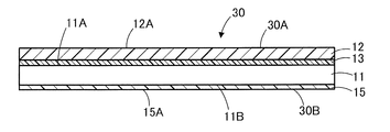
- the optical film 10 shown in FIG. 1 is used for an image display device and can be folded.
- the optical film 10 is provided between the resin substrate 11, the functional layer 12 provided on the first surface 11A side which is one surface of the resin substrate 11, and the resin substrate 11 and the functional layer 12.
- a first optical adjustment layer 13 (hereinafter, also simply referred to as “optical adjustment layer 13”) adjacent to the functional layer 12 is provided.
- a second optical adjustment layer 14 (hereinafter simply referred to as “optical”) provided between the resin base material 11 and the first optical adjustment layer 13 and adjacent to the resin base material 11.
- the third optical adjustment layer 15 hereinafter referred to as “adjustment layer 14”) provided on the second surface 11B which is the surface opposite to the first surface 11A of the resin base material 11. It may be simply referred to as “optical adjustment layer 15”).
- the second optical adjustment layer 14 and / or the third optical adjustment layer 15 may not be provided.
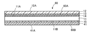
- the optical film 10 may further include a resin layer on the second surface 11B side of the resin base material 11 as in an optical film 40 described later.
- the “functional layer” in the present specification is a layer intended to exhibit some function in the optical film.
- examples of the functional layer include a hard coat layer, an antistatic layer, and an antifouling layer.
- the functional layer 12 functions as a hard coat layer.
- the functional layer 12 has a single layer structure, the functional layer may have not only a single layer structure but also a multilayer structure of two or more layers.
- each “optical adjustment layer” in the present specification has a single-layer structure and is not a multilayer structure of two or more layers.
- two optical adjustment layers, a first optical adjustment layer 13 and a second optical adjustment layer 14, are provided between the resin base material 11 and the functional layer 12.
- Another optical adjustment layer or the like may be further provided between the one optical adjustment layer 13 and the second optical adjustment layer 14 to form a structure of three or more layers.
- the surface 10 ⁇ / b> A of the optical film 10 is the surface 12 ⁇ / b> A of the functional layer 12.
- the surface of the optical film is used as meaning the surface of one side of the optical film, so that the surface opposite to the surface of the optical film is distinguished from the back surface in order to distinguish it from the surface of the optical film. Shall be called.
- the back surface 10 ⁇ / b> B of the optical film 10 is a surface 15 ⁇ / b> A on the side opposite to the surface on the resin base material 11 side in the optical adjustment layer 15.
- the optical film 10 can be folded. Specifically, the test (continuous folding test) of continuously folding the optical film 10 was repeated 10,000 times so that the functional layer 12 was inside and the distance between the opposing sides of the optical film 10 was 10 mm. Even if it is a case, it is preferable that a crack or a fracture
- the test in which the optical film 10 is continuously folded so that the functional layer 12 is on the outside and the distance between the opposing sides of the optical film 10 is 30 mm is repeated 10,000 times.
- the optical film 10 is not cracked or broken, and it is more preferable that the optical film 10 is not cracked or broken even when the continuous folding test is repeated 20,000 times. Even when repeated, it is more preferable that the optical film 10 is not cracked or broken.
- the continuous folding test in which the optical film 10 is continuously folded so that the functional layer 12 is on the inside is performed as follows.
- the side portion 10C of the optical film 10 and the side portion 10D opposite to the side portion 10C are fixed by the fixing portions 20 arranged in parallel, respectively.
- the optical film 10 may be arbitrary shapes, it is preferable that the optical film 10 in a continuous folding test is a rectangle (for example, rectangle of 30 mm x 100 mm).
- the fixing portion 20 is slidable in the horizontal direction.
- the functional layer 12 is on the inside, that is, the surface 10A of the optical film 10 is on the inside.
- the optical film 10 is deformed so as to be folded, and further, as shown in FIG. 2 (C), the optical film 10 is fixed to a position where the distance between two opposing side parts fixed by the fixing part 20 of the optical film 10 is 10 mm. After the part 20 is moved, the fixing part 20 is moved in the reverse direction to eliminate the deformation of the optical film 10.
- the optical film 10 can be folded by 180 ° by moving the fixing portion 20.
- a continuous folding test is performed so that the bent portion 10E of the optical film 10 does not protrude from the lower end of the fixed portion 20, and the interval when the fixed portion 20 is closest is controlled to 10 mm.
- the interval between the two opposing sides can be 10 mm.
- the outer diameter of the bent portion 10E is regarded as 10 mm.
- the thickness of the optical film 10 is a sufficiently small value compared with the interval (10 mm) of the fixed portion 20, the result of the continuous folding test of the optical film 10 is not affected by the difference in the thickness of the optical film 10. It can be regarded as not received.
- cracking or breaking occurs when the continuous folding test is repeated 10,000 times so that the functional layer 12 is on the inner side and the distance between the opposing sides of the optical film 10 is 10 mm. More preferably, no cracks or breaks occur when the continuous folding test is repeated 10,000 times so that the functional layer 12 is on the inside and the distance between opposing sides of the optical film 10 is 2 mm. Most preferably not.
- the side portion 10C of the optical film 10 and the side portion 10D facing the side portion 10C are separated by a distance of 10 mm between the side portion 10C and the side portion 10D.
- a folding stationary test is performed in which the optical film 10 is folded in a state where the optical film 10 is folded for 12 hours.
- the folding portion is released by removing the fixing portion 25 from the side portion 10D after the folding stationary test, and the opening angle ⁇ , which is the angle at which the optical film 10 naturally opens in the optical film 10 after 30 minutes at room temperature, is measured.
- the opening angle ⁇ of the optical film 10 is preferably 100 ° or more.
- the folding stationary test may be performed so that the optical film 10 is folded so that the functional layer 12 is on the inner side, or may be performed so that the optical film 10 is folded so that the functional layer 12 is on the outer side.
- the opening angle ⁇ is preferably 100 ° or more.
- the surface 10A of the optical film 10 (the surface 12A of the functional layer 12) has a hardness (pencil hardness) of 3H or more when measured by a pencil hardness test specified in JIS K5600-5-4: 1999. Preferably, it is 4H or more.
- the optical film 10 cut out to a size of 30 mm ⁇ 100 mm is fixed with cello tape (registered trademark) manufactured by Nichiban Co., Ltd. so that there is no folding or wrinkle on the glass plate, and the pencil hardness is applied to the surface of the optical film.
- the above-mentioned scratches refer to those that are visually observed through transmission observation of the surface of the optical film subjected to the pencil hardness test under a fluorescent lamp.
- the surface resistance value of the surface 10A of the optical film 10 is preferably 10 12 ⁇ / ⁇ or less.
- the surface resistance value can be measured using a resistivity meter (product name “HIRESTA-UP MCP-HT450”, manufactured by Mitsubishi Chemical Analytech Co., Ltd., probe: URS) in accordance with JIS K6911: 2006.
- the surface resistance value of the surface 10A of the optical film 10 is obtained by randomly measuring 10 surface resistance values of the surface 10A of the optical film 10 cut into a size of 50 mm ⁇ 50 mm, and calculating the arithmetic average of the measured surface resistance values at 10 locations. Value.
- the saturation voltage on the surface 10A of the optical film 10 is 0 kV when a voltage of 10 kV is applied from a distance of 50 mm from the surface 10A of the optical film 10 in an environment of 23 ° C. and 50% relative humidity. Is preferably exceeded.
- the saturation band voltage on the back surface 10B of the optical film 10 is 0 kV when a voltage of 10 kV is applied from a distance of 20 mm from the back surface 10B of the optical film 10 in an environment of 23 ° C. and 50% relative humidity. It is preferable to exceed.
- the saturation voltage is the maximum voltage that can be stored in the optical film.
- the saturation band voltage at 10A exceeds 0 kV, the position of a finger or the like can be detected by the touch sensor even when the optical film 10 is arranged closer to the viewer than the touch sensor.
- the saturation charge voltage can be measured using a charged charge decay rate measuring device (product name “H-0110”, manufactured by Shishido electrostatic Co., Ltd.).
- the saturation voltage is an arithmetic average value of values obtained by measuring three times for an optical film cut out to a size of 100 mm ⁇ 100 mm.
- the lower limit of the saturation band voltage is more preferably 0.1 kV or more, and the upper limit of the saturation band voltage is more preferably 3 kV or less.
- the optical film 10 preferably has a yellow index (YI) of 15 or less. If YI of the optical film 10 is 15 or less, the yellowishness of the optical film can be suppressed, and the optical film 10 can be applied to applications requiring transparency.
- the upper limit of the yellow index (YI) of the optical film 10 is more preferably 10 or less.
- the yellow index (YI) is a light source on the back side of an optical film cut into a size of 50 mm ⁇ 100 mm in a spectrophotometer (product name “UV-2450”, manufactured by Shimadzu Corporation, light source: tungsten lamp and deuterium lamp).
- the chromaticity tristimulus values X, Y, and Z are calculated from the transmittance of the optical film having a wavelength of 300 nm to 780 nm measured in a state of being arranged on the side according to the arithmetic expression described in JIS Z8722: 2009. It is a value calculated from X, Y, Z according to the arithmetic expression described in ASTM D1925: 1962.
- the upper limit of the yellow index (YI) of the optical film 10 is more preferably 10 or less.
- the yellow index (YI) is measured three times for one optical film, and is the arithmetic average value of the values obtained by measuring three times.
- the yellow index is calculated by reading the transmittance measurement data on a monitor connected to UV-2450 and checking the item “YI” in the calculation item. .
- the transmittance at a wavelength of 300 nm to 780 nm is measured by measuring the transmittance for at least 5 points between 1 nm and 1 nm before and after the wavelength 300 nm to 780 nm under the following conditions, and calculating the average value.
- the smoothing process may be performed at a delta of 5.0 nm.
- the yellow index (YI) of the optical film 10 for example, at least one of the resin base material 11, the functional layer 12, and the optical adjustment layers 13 and 14 contains a blue pigment that is a complementary color of yellow. Also good. Even if yellowishness becomes a problem due to the use of a polyimide base material as the resin base material, the yellow index of the optical film can be obtained by including a blue pigment in the resin base material 11 or the like. (YI) can be reduced.
- the blue pigment may be either a pigment or a dye.
- the optical film 10 when used in an organic light emitting diode display device, it is preferable to have both light resistance and heat resistance.
- the above-mentioned blue pigment polycyclic organic pigments, metal complex organic pigments, etc. are used in applications where light resistance is required because the degree of molecular breakage due to ultraviolet rays is small compared to the molecular dispersion of dyes and the light resistance is remarkably superior More specifically, phthalocyanine-based organic pigments and the like are preferable.
- the pigment is particle-dispersed with respect to the solvent, transparency inhibition due to particle scattering exists, and therefore it is preferable to put the particle size of the pigment dispersion in the Rayleigh scattering region.
- a dye that is molecularly dispersed in the solvent it is preferable to use a dye that is molecularly dispersed in the solvent as the blue pigment.
- Examples of the light source include a tungsten halogen (WI) lamp alone or a combination of a deuterium (D2) lamp and a tungsten halogen (WI) lamp.
- WI tungsten halogen
- D2 deuterium
- WI tungsten halogen
- “light with an incident angle of 0 °” means light in the normal direction when the normal direction of the first surface of the optical film is 0 °.
- “L * a * b * color system”, “a * ”, and “b * ” are based on JIS Z8729: 2004.
- the spectral transmittance at a wavelength of 380 nm of the optical film 10 is preferably 8% or less.
- the polarizer may be exposed to ultraviolet rays and may be easily deteriorated.
- the transmittance can be measured using a spectrophotometer (product name “UV-2450”, manufactured by Shimadzu Corporation).
- the measurement conditions of the spectral transmittance are the same as the measurement conditions of the spectral transmittance at the wavelength of 300 nm to 780 nm.
- permeability is measured 3 times with respect to the optical film cut out to the magnitude
- the upper limit of the transmittance of the optical film 10 is more preferably 5%.
- permeability of the optical film 10 can be achieved by adjusting the addition amount of the ultraviolet absorber mentioned later.
- the total light transmittance of the optical film 10 is preferably 85% or more. If the total light transmittance of the optical film 10 is 85% or more, sufficient image visibility can be obtained when the optical film 10 is used in a mobile terminal.
- the total light transmittance of the optical film 10 is more preferably 87% or more, and most preferably 90% or more.
- the total light transmittance can be measured by a method based on JIS K7361-1: 1997 using a haze meter (product name “HM-150”, manufactured by Murakami Color Research Laboratory Co., Ltd.).
- the total light transmittance is measured three times for one optical film after cutting the optical film into a size of 50 mm ⁇ 100 mm, placing it without curls or wrinkles, and without fingerprints or dust. It is set as the arithmetic average value of the value obtained by measuring 3 times.
- “measuring three times” means not measuring the same place three times, but measuring three different places.
- the visually observed surface 10A is flat, the layers to be laminated such as the functional layer 12 are also flat, and the variation in film thickness is within ⁇ 10%. Therefore, it is considered that the average value of the total light transmittance of the entire optical film in the whole plane can be obtained by measuring the total light transmittance at three different positions of the cut out optical film.
- the variation in the total light transmittance is within ⁇ 10% regardless of whether the object to be measured is as long as 1 m ⁇ 3000 m or the size of a 5-inch smartphone.
- HM-150 has an inlet opening for measurement of 20 mm.phi., So that the sample size needs to be 21 mm or more in diameter.
- the measurement points are set to three positions by gradually shifting within a range where the light source spot is not removed or changing the angle.
- the haze value (total haze value) of the optical film 10 is preferably 2.5% or less. If the said haze value of an optical film is 2.5% or less, when an optical film is used for a mobile terminal, whitening of an image display surface can be suppressed.
- the haze value is more preferably 1.5% or less, and more preferably 1.0% or less.
- the haze value can be measured by a method based on JIS K7136: 2000 using a haze meter (product name “HM-150”, manufactured by Murakami Color Research Laboratory Co., Ltd.).
- the haze value is measured three times for one optical film after cutting the optical film into a size of 50 mm ⁇ 100 mm, placing it without curls or wrinkles, and without fingerprints or dust.
- the visually observed surface 10A is flat, the layers to be laminated such as the functional layer 12 are also flat, and the variation in film thickness is within ⁇ 10%.
- the average value of the haze value of the approximate whole in-plane of an optical film is obtained by measuring a haze value in three different places of the cut-out optical film.
- the variation in the haze value is within ⁇ 10% regardless of whether the measurement target is as long as 1 m ⁇ 3000 m or the size of a 5-inch smartphone.
- HM-150 has an inlet opening for measurement of 20 mm.phi., So that the sample size needs to be 21 mm or more in diameter. For this reason, you may cut out an optical film suitably in the magnitude
- the measurement points are set to three positions by gradually shifting within a range where the light source spot is not removed or changing the angle.
- the other film When another film such as a polarizing plate is provided on the first surface side of the optical film 10 via an adhesive layer or an adhesive layer, the other film is peeled off together with the adhesive layer or the adhesive layer, and then folded.
- Other films can be peeled as follows, for example. First, the laminate with other films attached to the optical film through an adhesive layer or adhesive layer is heated with a dryer, and the blade edge of the cutter is inserted into the part that appears to be the interface between the optical film and the other film. I will do it. By repeating such heating and peeling, the pressure-sensitive adhesive layer, the adhesive layer, and other films can be peeled off.
- the haze value is measured after the adhesive layer or the adhesive layer is peeled off, and the dirt on the adhesive layer or the adhesive layer is further wiped off with alcohol.
- a light emitting diode (Light Emitting Diode) has been actively adopted as a light source for a backlight of an image display device such as a personal computer or a tablet terminal.
- the light emitting diode strongly emits light called blue light. .
- This blue light is a light with a wavelength of 380 nm to 495 nm and has a property close to that of ultraviolet rays. Since it has strong energy, it reaches the retina without being absorbed by the cornea or the crystalline lens. It is said to cause serious fatigue and adverse effects on sleep. For this reason, when an optical film is applied to an image display device, it is preferable that the optical film has excellent blue light shielding properties without affecting the color of the display screen.
- the optical film 10 has a spectral transmittance of less than 1% at a wavelength of 380 nm, a spectral transmittance of less than 10% at a wavelength of 410 nm, and a spectral transmittance of 70 at a wavelength of 440 nm. % Or more is preferable. If the spectral transmittance at a wavelength of 380 nm is 1% or more or the spectral transmittance at a wavelength of 410 nm is 10% or more, the problem due to blue light may not be solved, and the spectral transmittance at a wavelength of 440 nm is 70%.
- the optical film 10 sufficiently absorbs light in the wavelength region of 410 nm or less of the wavelength of blue light, while sufficiently transmitting light of wavelength 440 nm or more without affecting the color of the display screen. Blue light shielding properties can be improved. Moreover, when the optical film 10 having excellent blue light shielding properties is applied to an organic light emitting diode (OLED) display device as an image display device, it is also effective in suppressing deterioration of the organic light emitting diode element.
- OLED organic light emitting diode
- the light transmittance of the optical film 10 is almost 0% up to a wavelength of 380 nm, it is preferable that the light transmission gradually increases from a wavelength of 410 nm, and the light transmission rapidly increases in the vicinity of a wavelength of 440 nm.
- the spectral transmittance changes between a wavelength of 410 nm and 440 nm so as to draw a sigmoid curve.
- the spectral transmittance at a wavelength of 380 nm is more preferably less than 0.5%, still more preferably less than 0.2%, and the spectral transmittance at a wavelength of 410 nm is more preferably less than 7%, more preferably less than 5%.
- the spectral transmittance at a wavelength of 440 nm is more preferably 75% or more, and still more preferably 80% or more.
- the optical film 10 preferably has a spectral transmittance of less than 50% at a wavelength of 420 nm. By satisfying such a spectral transmittance relationship, the optical film 10 has a sharply improved transmittance around a wavelength of 440 nm, and has an excellent blue light shielding property without affecting the color of the display screen. Can be obtained.
- the spectral transmittance at a wavelength of 380 nm in the optical film 10 is more preferably less than 0.1%, the spectral transmittance at a wavelength of 410 nm is more preferably less than 7%, and the spectral transmittance at a wavelength of 440 nm is 80% or more. It is more preferable that
- the slope of the transmission spectrum in the wavelength range of 415 to 435 nm obtained by using the least square method is larger than 2.0.
- the inclination is 2.0 or less, light cannot be sufficiently cut in the blue light wavelength region, for example, the wavelength region of 415 to 435 nm, and the blue light cut effect may be weakened. Further, there is a possibility that the light wavelength region of blue light (wavelength 415 to 435 nm) is cut too much. In that case, the backlight of the image display device or the light emission wavelength region (for example, light emission from the wavelength 430 nm of the OLED) There is a possibility that a problem such as a problem that the color becomes worse due to interference with the color is increased.
- a spectrophotometer (product name “UV-2450”, manufactured by Shimadzu Corporation) capable of measuring in increments of 0.5 nm is used for the inclination, and transmittance data for at least 5 points between 1 nm and 1 nm is obtained. It can be calculated by measuring between 415 and 435 nm.
- the optical film 10 preferably has a blue light shielding rate of 40% or more. If the blue light shielding rate is less than 40%, the above-described problems caused by blue light may not be sufficiently solved.
- the blue light shielding rate is, for example, a value calculated according to JIS T7333: 2005. Such a blue light shielding rate can be achieved, for example, when the functional layer 12 contains a sesamol type benzotriazole-based monomer described later.
- the use of the optical film 10 is not particularly limited. Examples of the use of the optical film 10 include image display devices such as smartphones, tablet terminals, personal computers (PCs), wearable terminals, digital signage, televisions, and car navigation systems. Can be mentioned.
- the optical film 10 is also suitable for in-vehicle use.
- the form of each image display device is also preferable for applications that require flexibility such as foldable and rollable.
- the optical film 10 may be cut into a desired size, but may be in a roll shape.
- the size of the optical film is not particularly limited, and is appropriately determined according to the size of the display surface of the image display device.
- the size of the optical film 10 may be, for example, not less than 2.8 inches and not more than 500 inches.
- “inch” means the length of a diagonal line when the optical film has a quadrangular shape, means the diameter when the optical film is circular, and has the short diameter when it is elliptical. And the average value of the sum of the major axes.
- the aspect ratio of the optical film when obtaining the inch is not particularly limited as long as there is no problem as a display screen of the image display device.
- length: width 1: 1, 4: 3, 16:10, 16: 9, 2: 1, and the like.
- the aspect ratio is not particularly limited in in-vehicle applications and digital signage that are rich in design.
- size of the optical film 10 is large, after cutting out to A5 size (148 mm x 210 mm) from arbitrary positions, it shall cut out to the magnitude
- the location of the optical film 10 in the image display device may be inside the image display device, but is preferably near the surface of the image display device.
- the optical film 10 When used near the surface of the image display device, the optical film 10 functions as a cover film used instead of the cover glass.
- the resin base material 11 has light transmittance.
- the “light transmittance” in the present specification means a property of transmitting light.
- the total light transmittance is 50% or more, preferably 70% or more, more preferably 80% or more, and particularly preferably 90%. Including that.
- the light transmissive property does not necessarily need to be transparent, and may be translucent.
- the resin substrate 11 is a group composed of one or more resins selected from the group consisting of polyimide resins, polyamideimide resins, polyamide resins, and polyester resins (for example, polyethylene terephthalate resins and polyethylene naphthalate resins). It is a material.
- a polyimide resin, a polyamide resin, or a mixture thereof is preferable.
- the polyimide resin is obtained by reacting a tetracarboxylic acid component and a diamine component.
- a tetracarboxylic acid component and a diamine component.
- polyimide-type resin selects from the group which consists of a structure represented by following General formula (1) and following General formula (3) from the point which has the outstanding light transmittance and the outstanding rigidity. It is preferable to have at least one kind of structure.
- R 1 is a tetravalent group which is a tetracarboxylic acid residue
- R 2 is a trans-cyclohexanediamine residue, a trans-1,4-bismethylenecyclohexanediamine residue
- 4,4 It represents at least one divalent group selected from the group consisting of a '-diaminodiphenylsulfone residue, a 3,4'-diaminodiphenylsulfone residue, and a divalent group represented by the following general formula (2).
- n represents the number of repeating units and is 1 or more.
- tetracarboxylic acid residue means a residue obtained by removing four carboxyl groups from tetracarboxylic acid, and a residue obtained by removing an acid dianhydride structure from tetracarboxylic dianhydride; Represents the same structure.
- diamine residue refers to a residue obtained by removing two amino groups from a diamine.
- R 3 and R 4 each independently represent a hydrogen atom, an alkyl group, or a perfluoroalkyl group.
- R 5 represents a cyclohexanetetracarboxylic acid residue, a cyclopentanetetracarboxylic acid residue, a dicyclohexane-3,4,3 ′, 4′-tetracarboxylic acid residue, and 4,4 ′.
- At least one tetravalent group selected from the group consisting of-(hexafluoroisopropylidene) diphthalic acid residues R 6 represents a divalent group that is a diamine residue.
- n ′ represents the number of repeating units and is 1 or more.
- R 1 is a tetracarboxylic acid residue, and can be a residue obtained by removing the acid dianhydride structure from the tetracarboxylic dianhydride as exemplified above.
- R 1 in the general formula (1) is, among others, 4,4 ′-(hexafluoroisopropylidene) diphthalic acid residue, 3,3 ′, from the viewpoint of improving light transmittance and improving rigidity.
- these suitable residues are preferably contained in a total amount of 50 mol% or more, more preferably 70 mol% or more, and still more preferably 90 mol% or more.
- R 1 is selected from the group consisting of 3,3 ′, 4,4′-biphenyltetracarboxylic acid residue, 3,3 ′, 4,4′-benzophenonetetracarboxylic acid residue, and pyromellitic acid residue.
- a group of tetracarboxylic acid residues (group A) suitable for improving rigidity such as at least one selected from 4,4 ′-(hexafluoroisopropylidene) diphthalic acid residues, 2,3 ′ , 3,4′-biphenyltetracarboxylic acid residue, 3,3 ′, 4,4′-diphenylsulfonetetracarboxylic acid residue, 4,4′-oxydiphthalic acid residue, cyclohexanetetracarboxylic acid residue, and cyclohexane
- group B suitable for improving transparency, such as at least one selected from the group consisting of pentanetetracarboxylic acid residues.
- the content ratio of the tetracarboxylic acid residue group (group A) suitable for improving the rigidity and the tetracarboxylic acid residue group (group B) suitable for improving transparency is, 0.05 mol of the tetracarboxylic acid residue group (group A) suitable for improving the rigidity is 1 mol per 1 mol of the tetracarboxylic acid residue group (group B) suitable for improving the transparency. It is preferably 9 mol or less, more preferably 0.1 mol or more and 5 mol or less, still more preferably 0.3 mol or more and 4 mol or less.
- R 2 in the general formula (1) is, among others, 4,4′-diaminodiphenylsulfone residue, 3,4′-diaminodiphenylsulfone residue from the viewpoint of improving light transmittance and improving rigidity.
- at least one divalent group selected from the group consisting of a divalent group represented by the general formula (2) and is preferably a 4,4′-diaminodiphenylsulfone residue, 3 , 4′-diaminodiphenylsulfone residue, and at least one divalent group selected from the group consisting of a divalent group represented by the general formula (2) wherein R 3 and R 4 are perfluoroalkyl groups
- the group is preferably.
- R 5 in the general formula (3) is, among others, 4,4 ′-(hexafluoroisopropylidene) diphthalic acid residue, 3,3 ′, from the viewpoint of improving light transmittance and improving rigidity. It preferably contains a 4,4′-diphenylsulfone tetracarboxylic acid residue and an oxydiphthalic acid residue.
- these suitable residues are preferably contained in an amount of 50 mol% or more, more preferably 70 mol% or more, and even more preferably 90 mol% or more.
- R 6 in the general formula (3) is a diamine residue, and can be a residue obtained by removing two amino groups from the diamine as exemplified above.
- R6 in the general formula (3) is, among others, a 2,2′-bis (trifluoromethyl) benzidine residue, bis [4- (4- Aminophenoxy) phenyl] sulfone residue, 4,4′-diaminodiphenylsulfone residue, 2,2-bis [4- (4-aminophenoxy) phenyl] hexafluoropropane residue, bis [4- (3-amino Phenoxy) phenyl] sulfone residue, 4,4′-diamino-2,2′-bis (trifluoromethyl) diphenyl ether residue, 1,4-bis [4-amino-2- (trifluoromethyl) phenoxy] benzene Residue, 2,2-bis [4- (4-amino-2-trifluoromethylphenoxy)
- these suitable residues are preferably contained in a total amount of 50 mol% or more, more preferably 70 mol% or more, and still more preferably 90 mol% or more.
- R 6 is a bis [4- (4-aminophenoxy) phenyl] sulfone residue, 4,4′-diaminobenzanilide residue, N, N′-bis (4-aminophenyl) terephthalamide residue, A group of diamine residues suitable for improving the rigidity such as at least one selected from the group consisting of a paraphenylenediamine residue, a metaphenylenediamine residue, and a 4,4′-diaminodiphenylmethane residue (group) C), 2,2′-bis (trifluoromethyl) benzidine residue, 4,4′-diaminodiphenylsulfone residue, 2,2-bis [4- (4-aminophenoxy) phenyl] hexafluoropropane residue Group, bis [4- (3-aminophenoxy) phenyl] sulfone residue, 4,4′-diamino-2,2′-bis (trifluoromethyl) diphen
- the content ratio of the diamine residue group (group C) suitable for improving the rigidity and the diamine residue group (group D) suitable for improving transparency improves transparency.
- the diamine residue group (group C) suitable for improving the rigidity is 0.05 mol or more and 9 mol or less with respect to 1 mol of the diamine residue group (group D) suitable for the treatment. More preferably, it is preferably 0.1 mol or more and 5 mol or less, and more preferably 0.3 mol or more and 4 mol or less.
- the number of repeating units n in the polyimide is not particularly limited as long as it is appropriately selected depending on the structure so as to exhibit a preferable glass transition temperature described later.
- the average number of repeating units is usually 10 to 2000, and more preferably 15 to 1000.
- the polyimide resin may contain a polyamide structure in a part thereof.
- the polyamide structure examples include a polyamideimide structure containing a tricarboxylic acid residue such as trimellitic anhydride and a polyamide structure containing a dicarboxylic acid residue such as terephthalic acid.
- the polyimide resin preferably has a glass transition temperature of 250 ° C. or higher, and more preferably 270 ° C. or higher, from the viewpoint of heat resistance.
- the glass transition temperature is preferably 400 ° C. or lower, and more preferably 380 ° C. or lower, from the viewpoint of easy stretching and reduction of the baking temperature.
- Examples of the polyimide resin include compounds having a structure represented by the following formula.
- n is a repeating unit and represents an integer of 2 or more.
- polyimide resins a polyimide resin or a polyamide resin having a structure in which charge transfer within a molecule or between molecules is unlikely to occur is preferable, and specifically, the above formula (4).
- Fluorinated polyimide resins such as (11) to (11), and polyimide resins having an alicyclic structure such as the above formulas (13) to (16).
- the fluorinated polyimide resins of the above formulas (4) to (11) have a fluorinated structure, they have high heat resistance, and heat during the production of a polyimide film made of the polyimide resin. Since it is not colored by, it has the outstanding transparency.
- Polyamide resin is a concept including not only aliphatic polyamide but also aromatic polyamide (aramid).
- examples of the polyamide-based resin include compounds having a skeleton represented by the following formulas (21) to (23).
- n is a repeating unit and represents an integer of 2 or more.
- Examples of the commercially available base material made of the polyimide-based resin include Neoprim manufactured by Mitsubishi Gas Chemical Co., Ltd., and examples of the commercially available base material made of the polyamide-based resin include Mikutron manufactured by Toray Industries, Inc. Is mentioned.
- the polyimide resin or polyamide resin represented by the above formulas (4) to (20) and (23) may be synthesized by a known method.
- a method for synthesizing a polyimide resin represented by the above formula (4) is described in Japanese Patent Application Laid-Open No. 2009-132091, and specifically, 4,4′-hexa represented by the following formula (24): It can be obtained by reacting fluoropropylidenebisphthalic dianhydride (FPA) with 2,2′-bis (trifluoromethyl) -4,4′-diaminobiphenyl (TFDB).
- FPA fluoropropylidenebisphthalic dianhydride
- TFDB 2,2′-bis (trifluoromethyl) -4,4′-diaminobiphenyl
- the weight average molecular weight of the polyimide resin or polyamide resin is preferably in the range of 3000 to 500,000, more preferably in the range of 5000 to 300,000, and in the range of 10,000 to 200,000. More preferably. When the weight average molecular weight is less than 3000, sufficient strength may not be obtained. When the weight average molecular weight exceeds 500,000, the viscosity increases and the solubility decreases, so that a substrate having a smooth surface and a uniform film thickness can be obtained. It may not be obtained.
- the “weight average molecular weight” is a polystyrene conversion value measured by gel permeation chromatography (GPC).
- the resin substrate 11 is a fluorinated polyimide resin represented by the above formulas (4) to (11) or a polyamide system having a halogen group such as the above formula (23) from the viewpoint of improving the hardness. It is preferable to use a substrate made of a resin. Especially, it is more preferable to use the base material which consists of a polyimide-type resin represented by the said Formula (4) from a viewpoint which can improve hardness more.
- polyester-based resin examples include resins having at least one of polyethylene terephthalate, polypropylene terephthalate, polybutylene terephthalate, and polyethylene naphthalate as constituent components.
- the refractive index of the resin base material 11 is higher than the refractive index of the functional layer 12.
- the refractive index of the resin base material 11 can be measured by, for example, the Becke method.
- the refractive index of the resin base material 11 is measured using the Becke method, ten pieces of the resin base material 11 are cut out, and the refractive index is determined by the Becke method using the refractive index standard solution in the cut out ten pieces. Each of them is measured, and the average value of ten measured refractive indexes of the fragments is taken as the refractive index of the resin base material 11.
- the refractive index of the resin base material 11 may be 1.500 or more and 1.800 or less.
- the refractive index of the resin substrate 11 is obtained by measuring the average reflectance at a wavelength of 380 to 780 nm using a spectrophotometer (product name “UV-2450”, manufactured by Shimadzu Corporation), and obtaining the average reflectance. May be obtained by the following equation (1).
- the average reflectance (R) of the resin substrate 11 is such that a black vinyl tape having a width larger than the measurement spot area (for example, product name “Yamato Vinyl Tape NO200-38-21”, manufactured by Yamato Co., Ltd.) is used to prevent back surface reflection. , 38 mm width) is attached to the back surface of the resin base material 11 and then measured.
- R 1 (1-n 1 ) 2 / (1 + n 1) 2 ... (1)
- R 1 represents the average reflectance (%) of the resin substrate at a wavelength of 380 to 780 nm
- n 1 represents the refractive index of the resin substrate.
- the thickness of the resin base material 11 is preferably 10 ⁇ m or more and 100 ⁇ m or less. If the thickness of the resin substrate is 10 ⁇ m or more, curling of the optical film can be suppressed and sufficient hardness can be obtained, and even when the optical film is manufactured by Roll to Roll, wrinkles are generated. There is no risk of deterioration of the appearance. On the other hand, when the thickness of the resin base material is 100 ⁇ m or less, the optical film has good folding performance, can satisfy the requirements of the continuous folding test, and is preferable in terms of weight reduction of the optical film.
- the thickness of the resin base material 11 is obtained by taking a cross-section of the resin base material 11 using a scanning electron microscope (SEM), measuring the thickness of the resin base material 11 at 10 points in the cross-sectional image, The arithmetic average value of the film thickness.
- the lower limit of the resin base material 11 is more preferably 25 ⁇ m or more, and the upper limit of the resin base material 11 is more preferably 80 ⁇ m or less.
- the functional layer 12 is a layer that functions as a hard coat layer.
- the functional layer 12 may have a function other than the hard coat property in addition to the hard coat property.
- the functional layer 12 has antistatic properties in addition to hard coat properties. That is, the functional layer 12 is an antistatic hard coat layer.
- the “hard coat layer” in this specification means a layer having a Martens hardness of 375 MPa or more at the center of the cross section of the hard coat layer. In this specification, the “Martens hardness” is the hardness when the indenter is pushed in by 500 nm by the hardness measurement by the nanoindentation method.
- the measurement of the Martens hardness by the nanoindentation method is performed using “TI950 TriboIndenter” manufactured by HYSITRON Co., Ltd. for the measurement sample. Specifically, first, a block in which an optical film cut out to 1 mm ⁇ 10 mm is embedded with an embedding resin is prepared, and a uniform thickness without a hole or the like is obtained from this block by a general section manufacturing method. Cut the following sections. “Ultramicrotome EM UC7” (Leica Microsystems) can be used for preparing the slice. The remaining block from which a uniform section without holes or the like is cut out is taken as a measurement sample.
- the functional layer 12 preferably has a Martens hardness at the center of the cross section of the functional layer 12 of 500 MPa to 2000 MPa. If the Martens hardness of the functional layer 12 is 500 MPa or more, sufficient hardness as a hard coat layer can be obtained, and if it is 2000 MPa or less, good optical film folding performance can be obtained.
- the lower limit of the Martens hardness at the center of the cross section of the functional layer 12 is preferably 600 MPa or more, and the upper limit is preferably 1500 MPa or less.
- the refractive index of the functional layer 12 may be 1.400 or more and 1.800 or less.
- the refractive index of the functional layer 12 is determined by measuring an average reflectance at a wavelength of 380 to 780 nm using a spectrophotometer (product name “UV-2450”, manufactured by Shimadzu Corporation), and using the obtained average reflectance. The following equation (2) can be obtained.
- the average reflectance of the functional layer 12 is 1 to 10 ⁇ m thick when the composition for a functional layer is applied on a 50 ⁇ m thick polyethylene terephthalate (PET) base material that has not been subjected to an easy adhesion treatment and cured.
- PET polyethylene terephthalate
- a black vinyl tape having a width larger than the measurement spot area (for example, the product name “Yamato”) is formed on the surface (back surface) opposite to the functional layer side surface of the PET substrate. It is assumed that measurement is performed after affixing a vinyl tape NO200-38-21 "(manufactured by Yamato, 38 mm width).
- R 2 (1-n 2 ) 2 / (1 + n 2 ) 2 (2)
- R 2 represents the average reflectance (%) of the functional layer at a wavelength of 380 to 780 nm
- n 2 represents the refractive index of the functional layer.
- the film thickness of the functional layer 12 is preferably 2 ⁇ m or more and 40 ⁇ m or less. If the thickness of the functional layer 12 is 2 ⁇ m or more, sufficient hardness as a hard coat layer can be obtained, and if it is 40 ⁇ m or less, deterioration of workability can be suppressed.
- the “film thickness of the functional layer” means a film thickness (total thickness) obtained by adding up the film thicknesses of the respective functional layers when the functional layer has a multilayer structure.
- the upper limit of the functional layer 12 is more preferably 30 ⁇ m or less, and further preferably 20 ⁇ m or less.
- the thickness of the functional layer 12 is obtained by photographing a cross section of the functional layer 12 using a scanning transmission electron microscope (STEM) or a transmission electron microscope (TEM), and determining the thickness of the functional layer 12 in the image of the cross section. Twenty points are measured, and the arithmetic average value of the film thicknesses at the 20 points is taken. A specific method for taking a cross-sectional photograph is described below. First, a block in which an optical film cut out to a size of 1 mm ⁇ 10 mm is embedded with an embedding resin is produced, and a uniform thickness without a hole or the like is obtained from this block by a general section preparation method. Cut out sections.
- “Ultra Microtome EM UC7” Leica Microsystems Co., Ltd. or the like can be used.
- a uniform section having no holes or the like is used as a measurement sample.
- a cross-sectional photograph of the measurement sample is taken using a scanning transmission electron microscope (STEM) (product name “S-4800”, manufactured by Hitachi High-Technologies Corporation).
- STEM scanning transmission electron microscope
- the cross-section is observed with the detector set to “TE”, the acceleration voltage set to “30 kV”, and the emission current set to “10 ⁇ A”.
- the magnification is appropriately adjusted from 5000 to 200,000 times while adjusting the focus and observing whether each layer can be distinguished.
- a preferred magnification is 10,000 to 100,000 times, a more preferred magnification is 10,000 to 50,000 times, and a most preferred magnification is 25,000 to 50,000 times.
- the aperture is set to “beam monitor aperture 3”
- the objective lens aperture is set to “3”
- the W.S. D. May be set to “8 mm”.
- a dyeing process such as osmium tetroxide, ruthenium tetroxide, or phosphotungstic acid can be used to easily see the interface between the organic layers.
- the interface contrast may be difficult to understand when the magnification is high. In that case, the low magnification is also observed at the same time. For example, observe at two magnifications, high and low, such as 25,000 times and 50,000 times, and 50,000 times and 100,000 times, obtain the arithmetic average value described above at both magnifications, and further calculate the average value of the functional layer The value is the film thickness.
- the functional layer 12 is an antistatic hard coat layer, it includes a binder resin and an antistatic agent present in the binder resin. In addition, when the functional layer 12 is a hard coat layer having no antistatic property, the antistatic agent may not be included.
- the functional layer 12 is, for example, particles such as inorganic particles and organic particles, an ultraviolet absorber, an adhesion improver, and a leveling agent as long as the effects of the present invention are not impaired as required, in addition to a binder resin. Further, additives such as a thixotropic agent, a coupling agent, a plasticizer, an antifoaming agent, a filler, a colorant, and a filler may be included.
- the binder resin contains a polymer (cured product) of a polymerizable compound (curable compound).
- the polymerizable compound has at least one polymerizable functional group in the molecule.
- the polymerizable functional group include ethylenically unsaturated groups such as a (meth) acryloyl group, a vinyl group, and an allyl group.
- the “(meth) acryloyl group” means to include both “acryloyl group” and “methacryloyl group”.
- polyfunctional (meth) acrylate is preferable.
- the polyfunctional (meth) acrylate include trimethylolpropane tri (meth) acrylate, tripropylene glycol di (meth) acrylate, diethylene glycol di (meth) acrylate, dipropylene glycol di (meth) acrylate, pentaerythritol tri ( (Meth) acrylate, pentaerythritol tetra (meth) acrylate, dipentaerythritol hexa (meth) acrylate, 1,6-hexanediol di (meth) acrylate, neopentyl glycol di (meth) acrylate, trimethylolpropane tri (meth) acrylate , Ditrimethylolpropane tetra (meth) acrylate, dipentaerythritol penta (meth) acrylate, tripentaerythr
- those having 3 to 6 functional groups are preferable because they can satisfy the above-mentioned Martens hardness, and examples thereof include pentaerythritol triacrylate (PETA), dipentaerythritol hexaacrylate (DPHA), and pentaerythritol tetraacrylate (PETTA). Dipentaerythritol pentaacrylate (DPPA), trimethylolpropane tri (meth) acrylate, tripentaerythritol octa (meth) acrylate, tetrapentaerythritol deca (meth) acrylate, and the like are preferable.
- DPPA pentaerythritol triacrylate
- DPPA dipentaerythritol hexaacrylate
- PETTA pentaerythritol tetraacrylate
- Dipentaerythritol pentaacrylate (DPPA) trimethylolpropan
- a monofunctional (meth) acrylate monomer may be further included for adjusting the hardness, the viscosity of the composition, improving the adhesion, and the like.
- the monofunctional (meth) acrylate monomer include hydroxyethyl acrylate (HEA), glycidyl methacrylate, methoxypolyethylene glycol (meth) acrylate, isostearyl (meth) acrylate, 2-acryloyloxyethyl succinate, acryloylmorpholine, N -Acryloyloxyethyl hexahydrophthalimide, cyclohexyl acrylate, tetrahydrofuryl acrylate, isobornyl acrylate, phenoxyethyl acrylate, adamantyl acrylate and the like.
- HOA hydroxyethyl acrylate
- glycidyl methacrylate methoxypolyethylene glycol (meth) acrylate
- the weight average molecular weight of the monomer is preferably less than 1000, more preferably 200 or more and 800 or less, from the viewpoint of improving the hardness of the functional layer.
- the weight average molecular weight of the polymerizable oligomer is preferably 1000 or more and 20,000 or less, more preferably 1000 or more and 10,000 or less, and further preferably 2000 or more and 7000 or less.
- the antistatic agent used for the functional layer 12 is not particularly limited as long as it has good compatibility with the binder resin.
- the antistatic agent there are an ion conduction type antistatic agent and an electron conduction type antistatic agent, and from the viewpoint of compatibility with the binder resin, the ion conduction type antistatic agent is preferable.
- ion conduction type antistatic agent examples include cationic antistatic agents such as quaternary ammonium salts and pyridium salts, and alkali metal salts such as sulfonic acid, phosphoric acid and carboxylic acid (for example, lithium salts, sodium salts, Anionic antistatic agents such as potassium salts), amphoteric antistatic agents such as amino acids and amino acid sulfate esters, and nonionic antistatic agents such as amino alcohols, glycerins, and polyethylene glycols.
- quaternary ammonium salts and lithium salts are preferable because they exhibit excellent compatibility with the binder resin.
- the electron conductive antistatic agent examples include conductive polymers such as polyacetylene-based and polythiophene-based conductive polymers, metal particles, and metal oxide particles.
- conductive polymers such as polyacetylene-based and polythiophene-based conductive polymers, metal particles, and metal oxide particles.
- antistatic agents, metal particles, and metal oxide particles in which a dopant is combined with a conductive polymer such as polyacetylene and polythiophene are preferable.
- electroconductive particle can also be contained in the said electroconductive polymer.
- the antistatic agent composed of the conductive polymer include polyacetylene, polyaniline, polythiophene, polypyrrole, polyphenylene sulfide, poly (1,6-heptadiyne), polybiphenylene (polyparaphenylene), polyparafinylene sulfide, Examples thereof include conductive polymers such as polyphenylacetylene, poly (2,5-thienylene), and derivatives thereof.
- a polythiophene-based conductive organic polymer for example, 3,4-ethylenedioxythiophene (for example, PEDOT)).
- the antistatic agent comprising the conductive organic polymer
- the antistatic property can be maintained over a long period of time with little humidity dependency, and also has high transparency, low haze, and high hard coat properties, particularly Pencil hardness and scratch resistance against steel wool can be remarkably improved.
- the metal constituting the metal particles is not particularly limited, and examples thereof include Au, Ag, Cu, Al, Fe, Ni, Pd, and Pt alone or an alloy of these metals. Further, no particular limitation is imposed on the metal oxide constituting the metal oxide particles, for example, tin oxide (SnO 2), antimony oxide (Sb 2 O 5), antimony doped tin oxide (ATO), indium tin oxide ( ITO), aluminum-doped zinc oxide (AZO), fluorine-doped tin oxide (FTO), zinc oxide (ZnO) and the like.
- tin oxide (SnO 2) antimony oxide (Sb 2 O 5), antimony doped tin oxide (ATO), indium tin oxide ( ITO), aluminum-doped zinc oxide (AZO), fluorine-doped tin oxide (FTO), zinc oxide (ZnO) and the like.
- an antistatic agent it does not specifically limit as content of an antistatic agent, It is preferable that it is 1 to 50 mass parts with respect to 100 mass parts of polymeric compounds of the composition for functional layers. If it is 1 part by mass or more, the above-described antistatic property can be sufficiently obtained, and if it is 50 parts by mass or less, a highly transparent film having a small haze value and good total light transmittance can be obtained.
- the lower limit of the content of the antistatic agent is more preferably 10 parts by mass or more, and the upper limit is more preferably 40 parts by mass or less.
- the functional layer 12 may further contain an ultraviolet absorber, a spectral transmittance adjusting agent, and / or an antifouling agent.
- the optical film is particularly preferably used for a mobile terminal such as a foldable smartphone or tablet terminal.
- a mobile terminal is often used outdoors, and therefore, the optical film is disposed closer to the display element than the optical film.
- the polarizer is easily deteriorated by being exposed to ultraviolet rays.
- the functional layer 12 is disposed on the viewer side of the polarizer, if the functional layer 12 contains an ultraviolet absorber, deterioration due to exposure of the polarizer to ultraviolet rays can be suitably prevented. it can.
- the said ultraviolet absorber may be contained in the resin base material 11 instead of the functional layer 12.
- ultraviolet absorbers examples include triazine-based ultraviolet absorbers, benzophenone-based ultraviolet absorbers, and benzotriazole-based ultraviolet absorbers.
- Examples of the triazine ultraviolet absorber include 2- (2-hydroxy-4- [1-octyloxycarbonylethoxy] phenyl) -4,6-bis (4-phenylphenyl) -1,3,5-triazine.
- benzophenone ultraviolet absorber examples include 2-hydroxybenzophenone, 2,4-dihydroxybenzophenone, 2,2′-dihydroxy-4,4′-dimethoxybenzophenone, 2,2 ′, 4,4′-tetrahydroxy. Examples thereof include benzophenone, 2-hydroxy-4-methoxybenzophenone, hydroxymethoxybenzophenone sulfonic acid and its trihydrate, hydroxymethoxybenzophenone sulfonate sodium, and the like. Examples of commercially available benzophenone ultraviolet absorbers include CHMASSORB81 / FL (manufactured by BASF).
- benzotriazole ultraviolet absorber examples include 2-ethylhexyl-3- [3-tert-butyl-4-hydroxy-5- (5-chloro-2H-benzotriazol-2-yl) phenyl] propionate, 2 -(2H-benzotriazol-2-yl) -6- (linear and side chain dodecyl) -4-methylphenol, 2- [5-chloro (2H) -benzotriazol-2-yl] -4-methyl- 6- (tert-butyl) phenol, 2- (2H-benzotriazol-2-yl) -4,6-di-tert-pentylphenol, 2- (2′-hydroxy-5′-methylphenyl) benzotriazole, 2- (2′-hydroxy-3 ′, 5′-di-tert-butylphenyl) benzotriazole, 2- (2′-hydroxy-3) -Tert-butyl-5'-methylphenyl) benzotriazole, 2- (2'-
- benzotriazole ultraviolet absorbers examples include KEMISORB71D, KEMISORB79 (all manufactured by Chemipro Kasei Co., Ltd.), JF-80, JAST-500 (all manufactured by Johoku Chemical Co., Ltd.), ULS-1933D (one side) And RUVA-93 (manufactured by Otsuka Chemical Co., Ltd.).
- triazine ultraviolet absorbers and benzotriazole ultraviolet absorbers are preferably used as the ultraviolet absorber. It is preferable that the ultraviolet absorber has high solubility with the resin component constituting the functional layer, and it is preferable that the bleedout after the continuous folding test described above is small.
- the ultraviolet absorber is preferably polymerized or oligomerized.
- a polymer or oligomer having a benzotriazole, triazine, or benzophenone skeleton is preferable. Specifically, (meth) acrylate having a benzotriazole or benzophenone skeleton and methyl methacrylate (MMA) at an arbitrary ratio. It is preferable that it has been heat copolymerized.
- the ultraviolet absorber can also serve to protect the OLED from ultraviolet rays.
- a ultraviolet absorber Although it does not specifically limit as content of a ultraviolet absorber, It is preferable that they are 1 mass part or more and 6 mass parts or less with respect to 100 mass parts of solid content of the composition for functional layers. If it is 1 mass part or more, the effect which makes the functional layer contain the ultraviolet absorber mentioned above can fully be acquired, and if it is 6 mass parts or less, remarkable coloring and strength reduction do not occur in the functional layer. As for the minimum of content of the said ultraviolet absorber, it is more preferable that it is 2 mass parts or more, and it is more preferable that an upper limit is 5 mass parts or less.
- the spectral transmittance adjusting agent adjusts the spectral transmittance of the optical film.
- the functional layer 12 contains a sesamol-type benzotriazole monomer represented by the following general formula (25)
- the above-described spectral transmittance can be preferably satisfied.
- R 7 represents a hydrogen atom or a methyl group.
- R 8 represents a linear or branched alkylene group having 1 to 6 carbon atoms or a linear or branched oxyalkylene group having 1 to 6 carbon atoms.
- the sesamol type benzotriazole monomer is not particularly limited, but specific substance names include 2- [2- (6-hydroxybenzo [1,3] dioxol-5-yl) -2H-benzo Triazol-5-yl] ethyl methacrylate, 2- [2- (6-hydroxybenzo [1,3] dioxol-5-yl) -2H-benzotriazol-5-yl] ethyl acrylate, 3- [2- (6 -Hydroxybenzo [1,3] dioxol-5-yl) -2H-benzotriazol-5-yl] propyl methacrylate, 3- [2- (6-hydroxybenzo [1,3] dioxol-5-yl) -2H -Benzotriazol-5-yl] propyl acrylate, 4- [2- (6-hydroxybenzo [1,3] dioxol-5-yl -2H-benzotriazol-5-yl] butyl methacrylate, 4- [2- (6-
- the antifouling agent is not particularly limited, and examples thereof include silicone antifouling agents, fluorine antifouling agents, silicone type and fluorine antifouling agents, which may be used alone or in combination. May be.
- the antifouling agent may be an acrylic antifouling agent.
- the content of the antifouling agent is preferably 0.01 to 3.0 parts by mass with respect to 100 parts by mass of the polymerizable compound described above. If it is 0.01 part by mass or more, sufficient antifouling performance can be imparted to the functional layer, and if it is 3.0 parts by mass or less, the hardness of the functional layer does not decrease.
- the antifouling agent preferably has a weight average molecular weight of 5000 or less, and is a compound having preferably 1 or more, more preferably 2 or more reactive functional groups in order to improve the durability of the antifouling performance. Among them, excellent scratch resistance can be imparted by using an antifouling agent having two or more reactive functional groups.
- the antifouling agent does not have a reactive functional group
- the antifouling agent is transferred to the back surface of the optical film when it is stacked, whether it is a roll or a sheet.
- the other layer may be peeled off and may be easily peeled off by performing a plurality of continuous folding tests.
- the antifouling agent having the reactive functional group has good antifouling performance durability (durability), and in particular, the functional layer containing the above-described fluorine-based antifouling agent is difficult to have a fingerprint ( Less noticeable) and good wiping property. Furthermore, since the surface tension at the time of application of the functional layer composition can be lowered, the leveling property is good, and the appearance of the functional layer to be formed is good.
- the functional layer containing a silicone-based antifouling agent has good sliding properties and good steel wool resistance.
- a touch sensor in which an optical film containing such a silicone antifouling agent is mounted on the functional layer has good tactile sensation because of good sliding when touched with a finger or a pen. Further, fingerprints are hardly attached to the functional layer (not easily noticeable), and the wiping property is improved. Furthermore, since the surface tension at the time of application of the functional layer composition can be lowered, the leveling property is good, and the appearance of the functional layer to be formed is good.
- silicone antifouling agents examples include SUA1900L10 (manufactured by Shin-Nakamura Chemical Co., Ltd.), SUA1900L6 (manufactured by Shin-Nakamura Chemical Co., Ltd.), Ebecryl 1360 (manufactured by Daicel Cytec Co., Ltd.), UT3971 (manufactured by Nippon Gosei Co., Ltd.), and BYKUV3500 (BIC Chemie).
- SUA1900L10 manufactured by Shin-Nakamura Chemical Co., Ltd.
- SUA1900L6 manufactured by Shin-Nakamura Chemical Co., Ltd.
- Ebecryl 1360 manufactured by Daicel Cytec Co., Ltd.
- UT3971 manufactured by Nippon Gosei Co., Ltd.
- BYKUV3500 BIC Chemie
- BYKUV3510 by Big Chemie
- BYKUV3570 by Big Chemie
- X22-164E X22-174BX
- X22-2426 KBM503, KBM5103
- TEGO-RAD2250 TEGO-RAD2300
- TEGO-RAD2200N TEGO-RAD2010
- TEGO-RAD2500 TEGO-RAD2600
- TEGO-RAD2700 manufactured by Evonik Japan
- Megafuck RS854 (DIC) Ltd. and the like.
- fluorine-based antifouling agents include, for example, OPTOOL DAC, OPTOOL DSX (manufactured by Daikin Industries, Ltd.), Megafuck RS71, Megafuck RS74 (manufactured by DIC), LINC152EPA, LINC151EPA, and LINC182UA (manufactured by Kyoeisha Chemical Co., Ltd.)
- the solvent include 650A, 601ENT, 602, and 602.
- Examples of commercially available antifouling agents having fluorine-based and silicone-based reactive functional groups include, for example, MegaFac RS851, MegaFac RS852, MegaFac RS853, MegaFac RS854 (manufactured by DIC), Opstar TU2225, Opstar TU2224 ( JSR), X71-1203M (Shin-Etsu Chemical Co., Ltd.) and the like.
- the optical adjustment layer 13 is a layer for suppressing the generation of interference fringes.
- the refractive index of the optical adjustment layer 13 is preferably lower than the refractive index of the resin substrate 11 and higher than the refractive index of the functional layer 12 from the viewpoint of suppressing the occurrence of interference fringes. Since the refractive index of the optical adjustment layer 13 can be measured by the same method as the refractive index of the functional layer, the description is omitted here.
- the difference in refractive index between the optical adjustment layer 13 and the functional layer 12 is preferably 0.005 or more and 0.100 or less. If this refractive index difference is 0.005 or more, interface reflection occurs between the optical adjustment layer 13 and the functional layer 12 but interference fringes cannot be visually recognized. Although some fringes are confirmed, it can be set to a level at which there is no problem in actual use.
- the lower limit of the refractive index difference is more preferably 0.007 or more, and the upper limit is more preferably 0.090 or less.
- the refractive index of the optical adjustment layer 13 may be 0.010 or more and 0.080 or less.
- the film thickness of the optical adjustment layer 13 is preferably 30 nm or more and 200 nm or less. If the thickness of the optical adjustment layer 13 is 30 nm or more, sufficient adhesion between the functional layer 12 and the optical adjustment layer 13 can be secured, and if it is 200 nm or less, interference fringes can be further suppressed and folded. Can be improved.
- the film thickness of the optical adjustment layer 13 is determined by the same method as that for the functional layer 12.
- the lower limit of the optical adjustment layer 13 is more preferably 50 nm or more, and the upper limit is more preferably 150 nm or less.
- the optical adjustment layer 13 may be composed only of a resin, but preferably contains a binder resin and particles for adjusting the refractive index.
- the binder resin of the optical adjustment layer 13 is selected from the group consisting of (meth) acrylic resin, cellulose resin, urethane resin, vinyl chloride resin, polyester resin, polyolefin resin, polycarbonate, nylon, polystyrene, and ABS resin. It is preferable that it is at least one selected resin.
- the particles of the optical adjustment layer 13 are at least one selected from the group consisting of low refractive index particles such as silica and magnesium fluoride, metal oxide particles such as titanium oxide and zirconium oxide, and inorganic pigments such as cobalt blue. Preferably there is. Among these, a combination of a polyester resin and metal oxide particles such as titanium oxide and zirconium oxide is more preferable from the viewpoint of adhesion and refractive index difference adjustment.
- the optical adjustment layer 13 may contain an antistatic agent in order to obtain antistatic properties.
- the optical adjustment layer 13 contains an antistatic agent
- the optical adjustment layer 13 also functions as an antistatic layer.
- the antistatic agent in the optical adjustment layer 13
- the surface resistance value on the surface 10 ⁇ / b> A of the optical film 10 can be further stabilized.
- the antistatic agent is included in the optical adjustment layer 13
- the surface resistance value on the surface 10 ⁇ / b> A of the optical film 10 can be further stabilized by including the antistatic agent in the functional layer 12.
- the antistatic agent contained in the optical adjustment layer 13 the same antistatic agent as described in the column of the functional layer 12 can be used, and therefore, the description thereof is omitted here.
- the optical adjustment layer 14 is a layer for improving the adhesion between the resin substrate 11 and the optical adjustment layer 13 mainly without generating interference fringes. By providing the optical adjustment layer 14 between the resin base material 11 and the optical adjustment layer 13, adhesion can be improved as compared with the case where the resin base material 11 and the optical adjustment layer 13 are in direct contact.
- the refractive index of the optical adjustment layer 14 is preferably lower than the refractive index of the resin substrate 11 and higher than the refractive index of the optical adjustment layer 13 from the viewpoint of interference fringes. Since the refractive index of the optical adjustment layer 14 can be measured by the same method as that of the functional layer 12, the description thereof is omitted here.
- the difference in refractive index between the optical adjustment layer 14 and the optical adjustment layer 13 is preferably 0.005 or more and 0.100 or less. . If this refractive index difference is 0.005 or more, interface reflection occurs between the optical adjustment layer 14 and the optical adjustment layer 13 but interference fringes cannot be visually recognized. If it is 0.100 or less, although some interference fringes are confirmed, the interference fringes can be set to a level that is not problematic in actual use.
- the lower limit of the refractive index difference is more preferably 0.007 or more, and the upper limit is more preferably 0.090 or less.
- the refractive index of the optical adjustment layer 13 may be 0.010 or more and 0.080 or less.
- the thickness of the optical adjustment layer 14 is preferably 30 nm or more and 200 nm or less. If the film thickness of the optical adjustment layer 14 is 30 nm or more, sufficient adhesion between the optical adjustment layer 13 and the optical adjustment layer 14 and the resin substrate 11 and the optical adjustment layer 14 can be secured, and if it is 200 nm or less, Due to the refractive index difference between the optical adjustment layer 14 and the optical adjustment layer 13, interference fringes are not generated, and the folding property can be improved.
- the film thickness of the optical adjustment layer 14 is determined by the same method as that for the functional layer 12.
- the lower limit of the optical adjustment layer 14 is more preferably 50 nm or more, and the upper limit is more preferably 150 nm or less.
- the optical adjustment layer 14 may be composed only of a resin, but preferably contains a binder resin and particles for adjusting the refractive index.
- the resin of the optical adjustment layer 14 is selected from the group consisting of (meth) acrylic resin, cellulose resin, urethane resin, vinyl chloride resin, polyester resin, polyolefin resin, polycarbonate, nylon, polystyrene, and ABS resin. It is preferable that it is at least one kind of resin.
- the particles of the optical adjustment layer 13 are at least one selected from the group consisting of low refractive index particles such as silica and magnesium fluoride, metal oxide particles such as titanium oxide and zirconium oxide, and inorganic pigments such as cobalt blue. Preferably there is. Among these, a combination of a polyester resin and metal oxide particles such as titanium oxide and zirconium oxide is more preferable from the viewpoint of adhesion and refractive index difference adjustment.
- the optical adjustment layer 14 may contain an antistatic agent in order to obtain antistatic properties.
- the optical adjustment layer 14 contains an antistatic agent
- the optical adjustment layer 14 also functions as an antistatic layer.
- the surface resistance value on the surface 10A of the optical film 10 can be further stabilized.
- the antistatic agent is included in the optical adjustment layer 14, the surface resistance value on the surface 10 ⁇ / b> A of the optical film 10 can be further stabilized by including the antistatic agent in the functional layer 12.
- the antistatic agent contained in the optical adjustment layer 14 the same antistatic agent as that described in the column of the functional layer 12 can be used, and therefore the description thereof is omitted here.
- the optical adjustment layer 15 is a layer that improves the light transmittance of the optical film 10.
- the refractive index of the optical adjustment layer 15 is higher than 1.000 which is the refractive index of air and lower than the refractive index of the resin base material 11. Since the refractive index of the optical adjustment layer 15 can be measured by the same method as the refractive index of the functional layer 12, the description is omitted here.
- the difference in refractive index between the resin substrate 11 and the optical adjustment layer 15 is preferably 0.005 or more and 0.700 or less. If this refractive index difference is 0.005 or more, the light transmittance of the optical film 10 can be improved, and if it is 0.700 or less, the transparency of the optical film 10 is not impaired.
- the lower limit of the refractive index difference is more preferably 0.010 or more, and the upper limit is more preferably 0.600 or less.
- the refractive index of the optical adjustment layer 15 may be 0.050 or more and 0.500 or less.
- the film thickness of the optical adjustment layer 15 is preferably 30 nm or more and 1 ⁇ m or less. If the film thickness of the optical adjustment layer 15 is 30 nm or more, the light transmittance of the optical film 10 can be further improved, and if it is 1 ⁇ m or less, deterioration of workability can be suppressed.
- the film thickness of the optical adjustment layer 15 can be obtained by the same method as that for the functional layer 12.
- the lower limit of the optical adjustment layer 15 is more preferably 50 nm or more, the upper limit is more preferably 700 nm or less, and further preferably 500 nm or less.
- the configuration of the optical adjustment layer 15 is not particularly limited as long as the refractive index is higher than 1.000 and lower than the refractive index of the resin base material 11.
- the optical adjustment layer 15 can be made of a resin.
- the optical adjustment layer 15 may include low refractive index particles having a refractive index lower than that of the resin in order to further reduce the refractive index.
- the optical adjustment layer 15 may contain an antistatic agent in order to obtain antistatic properties. When the optical adjustment layer 15 contains an antistatic agent, the optical adjustment layer 15 also functions as an antistatic layer. Further, the optical adjustment layer 15 may contain a color adjusting agent such as the spectral transmittance adjusting agent in order to adjust the color of the optical film 10.
- the resin is at least one selected from the group consisting of (meth) acrylic resin, cellulose resin, urethane resin, vinyl chloride resin, polyester resin, polyolefin resin, polycarbonate, nylon, polystyrene, and ABS resin. It is preferable that the resin is. Among these, from the viewpoint of adhesion with the resin base material 11, (meth) acrylic resins, urethane resins, polyester resins, and the like are preferable.
- Examples of the (meth) acrylic resin include polymethyl methacrylate.
- Examples of the cellulose resin include diacetyl cellulose, cellulose acetate propionate (CAP), and cellulose acetate butyrate (CAB).
- As said urethane type resin a urethane resin etc. are mentioned, for example.
- vinyl chloride resin examples include polyvinyl chloride and vinyl chloride-vinyl acetate copolymers.
- polyester-type resin a polyethylene terephthalate etc. are mentioned, for example.
- polyolefin resin polyethylene, a polypropylene, etc. are mentioned, for example.
- Low refractive index particles examples include solid or hollow particles made of silica or magnesium fluoride.
- hollow silica particles are preferable, and such hollow silica particles can be produced by, for example, the production method described in Examples in JP-A-2005-099778.
- the average particle size (average primary particle size) of the low refractive index particles is preferably 5 nm or more and 100 nm or less. When the average particle diameter of the low refractive index particles is within the above range, the transparency of the optical adjustment layer 15 is not impaired, and a good particle dispersion state is obtained.
- the average particle diameter of the low refractive index particles is the particle diameter of 20 low refractive index particles from the cross-sectional image of the optical adjustment layer 15 taken using a transmission electron microscope (TEM) or a scanning transmission electron microscope (STEM). Is determined as the arithmetic average value of the particle diameters of the 20 low refractive index particles.
- the lower limit of the average particle diameter of the low refractive index particles is more preferably 10 nm or more, the upper limit is more preferably 80 nm or less, and further preferably 70 nm or less.
- silica particles having reactive groups on the surface are preferably used, and reactive hollow silica particles are particularly preferable.
- Such silica particles having a reactive group on the surface can be prepared by surface-treating the silica particles with a silane coupling agent or the like.
- a method of treating the surface of the silica particles with a silane coupling agent a dry method in which the silane coupling agent is sprayed on the silica particles, or a wet method in which the silica particles are dispersed in a solvent and then the silane coupling agent is added and reacted. Etc.
- Antistatic agent As the antistatic agent contained in the optical adjustment layer 15, the same antistatic agent as described in the column of the functional layer 12 can be used, and therefore, the description thereof is omitted here.
- the optical film 10 can be produced as follows, for example. First, the second optical adjustment layer composition for forming the optical adjustment layer 14 is applied onto the first surface 11A of the resin base 11 by a coating device such as a bar coater, and the second optical adjustment layer 14 is applied. A coating film of the composition for the adjustment layer is formed.
- the 2nd composition for optical adjustment layers contains particles, such as binder resin precursor and a metal oxide, and a solvent.
- the “binder resin precursor” in the present specification is a component that becomes a binder resin by removing the solvent or by curing with heat or ionizing radiation.
- the binder resin precursor include solvent-drying resins and polymerizable compounds that are cured by heat or ionizing radiation.
- the ionizing radiation in this specification include visible light, ultraviolet rays, X-rays, electron beams, ⁇ rays, ⁇ rays, and ⁇ rays.
- the second optical adjustment layer composition contains at least one of low refractive index particles such as silica and magnesium fluoride, inorganic pigments such as cobalt blue, a leveling agent, and a polymerization initiator, if necessary. You may go out.
- the second optical adjustment layer composition may be a (meth) acrylic resin, a cellulose resin, or a urethane resin as necessary.
- One or more resins selected from the group consisting of vinyl chloride resin, polyolefin resin, polycarbonate, nylon, polystyrene, and ABS resin may be included.
- the coating film After forming the coating film of the composition for the second optical adjustment layer, the coating film is dried by, for example, heating at a temperature of 40 ° C. or more and 200 ° C. or less for 10 seconds to 120 seconds by various known methods, Is evaporated or cured, and if necessary, the coating film is irradiated with ionizing radiation such as ultraviolet rays to form the optical adjustment layer 14 adjacent to the resin substrate 11.
- ionizing radiation such as ultraviolet rays
- the first optical adjustment layer composition for forming the optical adjustment layer 13 is applied onto the optical adjustment layer 14 by a coating device such as a bar coater. Form a coating film.
- the 1st composition for optical adjustment layers contains particles, such as a binder resin precursor and a metal oxide, and a solvent.
- the first optical adjustment layer composition contains at least one of low refractive index particles such as silica and magnesium fluoride, an inorganic pigment such as cobalt blue, a leveling agent, and a polymerization initiator, if necessary. You may go out.
- the first optical adjustment layer composition may be a (meth) acrylic resin, a cellulose resin, or a urethane resin as necessary.
- One or more resins selected from the group consisting of vinyl chloride resin, polyolefin resin, polycarbonate, nylon, polystyrene, and ABS resin may be included.
- the coating film of the first optical adjustment layer composition After forming the coating film of the first optical adjustment layer composition, the coating film is dried by heating at a temperature of, for example, 40 ° C. to 200 ° C. for 10 seconds to 120 seconds by various known methods, The optical adjustment layer 13 is formed by evaporating or curing the film and irradiating the coating film with ionizing radiation such as ultraviolet rays as necessary.
- ionizing radiation such as ultraviolet rays as necessary.
- a functional layer composition for forming the functional layer 12 is applied onto the optical adjustment layer 13 by a coating device such as a bar coater, and a coating film of the functional layer composition Form.
- the functional layer composition contains a polymerizable compound that becomes a binder resin after curing.
- the functional layer composition may contain an antistatic agent, an ultraviolet absorber, a spectral transmittance adjusting agent, an antifouling agent, inorganic particles, a leveling agent, a solvent, and a polymerization initiator, if necessary.
- solvent examples include alcohols (eg, methanol, ethanol, propanol, isopropanol, n-butanol, s-butanol, t-butanol, benzyl alcohol, PGME, ethylene glycol, diacetone alcohol), ketones (eg, acetone, methyl ethyl ketone, Methyl isobutyl ketone, cyclopentanone, cyclohexanone, heptanone, diisobutyl ketone, diethyl ketone, diacetone alcohol), ester (methyl acetate, ethyl acetate, butyl acetate, n-propyl acetate, isopropyl acetate, methyl formate, PGMEA), aliphatic Hydrocarbons (eg, hexane, cyclohexane), halogenated hydrocarbons (eg, methylene chloride, chloroform,
- alcohols
- solvents may be used alone or two or more of them may be used in combination.
- methyl isobutyl ketone and methyl ethyl ketone are preferable at the point which can dissolve or disperse
- the polymerization initiator is a component that is decomposed by irradiation with ionizing radiation to generate radicals to initiate or advance polymerization (crosslinking) of the polymerizable compound.
- the polymerization initiator is not particularly limited as long as it can release a substance that initiates radical polymerization by irradiation with ionizing radiation.
- the polymerization initiator is not particularly limited, and known ones can be used. Specific examples include, for example, acetophenones, benzophenones, Michler benzoylbenzoate, ⁇ -amyloxime ester, thioxanthones, propiophenone. , Benzyls, benzoins, acylphosphine oxides. Further, it is preferable to use a mixture of photosensitizers, and specific examples thereof include n-butylamine, triethylamine, poly-n-butylphosphine and the like.
- the coating film of the functional layer composition After forming the coating film of the functional layer composition, the coating film is dried by heating at a temperature of 30 ° C. or more and 120 ° C. or less for 10 seconds to 120 seconds by various known methods, and the solvent is evaporated.
- the coating film After drying the coating film, the coating film is irradiated with ionizing radiation such as ultraviolet rays to cure the coating film. Thereby, the functional layer 12 adjacent to the optical adjustment layer 13 is formed.
- ionizing radiation such as ultraviolet rays
- the third optical adjustment layer composition for forming the optical adjustment layer 15 is applied onto the second surface 11B of the resin base material 11 by a coating device such as a bar coater. Then, a coating film of the third composition for optical adjustment layer is formed.
- the 3rd composition for optical adjustment layers contains the resin precursor and the solvent.
- the third optical adjustment layer composition may further contain at least one of low refractive index particles, an antistatic agent, an inorganic pigment such as cobalt blue, a leveling agent, and a polymerization initiator, if necessary. Good.
- the third optical adjustment layer composition may be a (meth) acrylic resin, a cellulose-based resin, a urethane-based resin, One or more kinds of resins selected from the group consisting of vinyl chloride resin, polyolefin resin, polycarbonate, nylon, polystyrene, and ABS resin may be included. Since the solvent is the same as the solvent described in the column of the functional layer composition, the description is omitted here.
- the coating film of the third optical adjustment layer composition After forming the coating film of the third optical adjustment layer composition, the coating film is dried by heating at a temperature of, for example, 40 ° C. or more and 200 ° C. or less for 10 seconds to 120 seconds by various known methods, The optical adjustment layer 15 is formed by evaporating or curing the film and irradiating the coating film with ionizing radiation such as ultraviolet rays as necessary. Thereby, the optical film 10 shown in FIG. 1 is obtained.
- ionizing radiation such as ultraviolet rays
- the optical film may be the optical film 30, 40, 50, 60 shown in FIGS.
- the optical films 30, 40, 50, and 60 shown in FIGS. 4 to 7 are also used in the image display device and can be folded.
- the optical film 30 shown in FIG. 4 is provided between the resin base material 11, the functional layer 12 provided on the first surface 11A side of the resin base material 11, and the resin base material 11 and the functional layer 12.
- the optical adjustment layer 13 adjacent to the functional layer 12 is provided.
- the optical adjustment layer 14 is not provided, and the optical adjustment layer 13 is adjacent to the functional layer 12 and the resin base material 11. Since the physical properties of the optical film 30 are the same as the physical properties of the optical film 10, the description thereof will be omitted here.
- the surface 30A of the optical film 30 is the surface 12A of the functional layer 12, and the back surface 30B of the optical film 30 is the surface 15A opposite to the surface of the optical adjustment layer 15 on the resin base material 11 side. .
- the optical film 40 shown in FIG. 5 is provided between the resin base material 11, the functional layer 12 provided on the first surface 11A side of the resin base material 11, and the resin base material 11 and the functional layer 12.
- the optical adjustment layer 13 adjacent to the functional layer 12 and the resin layer 41 provided on the second surface 11B of the resin substrate 11 are provided.
- the optical adjustment layer 14 is not provided, and the optical adjustment layer 13 is adjacent to the functional layer 12 and the resin base material 11.
- the surface 40A of the optical film 40 is the surface 12A of the functional layer 12, and the back surface 30B of the optical film 40 is a surface 41A opposite to the surface of the resin layer 41 on the resin base material 11 side.
- the optical film 50 shown in FIG. 6 is provided between the resin base material 11, the functional layer 12 provided on the first surface 11A side of the resin base material 11, and the resin base material 11 and the functional layer 12.
- the optical adjustment layer 13 adjacent to the functional layer 12, the resin layer 41 provided on the second surface 11B side of the resin base material 11, and the resin base material 11 provided between the resin base material 11 and the resin layer 41.
- an optical adjustment layer 15 adjacent to.
- the optical adjustment layer 14 is not provided, and the optical adjustment layer 13 is adjacent to the functional layer 12 and the resin base material 11.
- the surface 50A of the optical film 50 is the surface 12A of the functional layer 12, and the back surface 50B of the optical film 50 is a surface 41A opposite to the surface of the resin layer 41 on the resin base material 11 side.
- the optical film 60 shown in FIG. 7 is provided between the resin base material 11, the functional layer 12 provided on the first surface 11A side of the resin base material 11, and the resin base material 11 and the functional layer 12.
- the optical adjustment layer 13 adjacent to the functional layer 12, the optical adjustment layer 14 provided between the resin base material 11 and the optical adjustment layer 13 and adjacent to the resin base material 11, and the second surface of the resin base material 11 A resin layer 41 provided on the 11B side, and an optical adjustment layer 15 provided between the resin base material 11 and the resin layer 41 and adjacent to the resin base material 11 are provided.
- the surface 60A of the optical film 60 is the surface 12A of the functional layer 12, and the back surface 60B of the optical film 60 is a surface 41A opposite to the surface of the resin layer 41 on the resin base material 11 side. Yes.
- the shear storage elastic modulus G ′ in the frequency range of 25 ° C. and 500 Hz to 1000 Hz is more than 200 MPa and 1200 MPa or less. If the shear storage modulus G ′ of the film exceeds 200 MPa, when an impact is applied to the surface of the optical film, not only the deformation of the optical film itself but also the adhesive layer is disposed inside the image display device rather than the optical film. Even in this case, plastic deformation of the adhesive layer can be suppressed. Moreover, if the shear storage elastic modulus G ′ of the optical films 40, 50, 60 is 1200 MPa or less, the optical film 40 can be prevented from cracking during folding.
- the lower limit of the shear storage modulus G ′ of the optical films 40, 50, 60 is preferably 400 MPa or more, and more preferably 500 MPa or more. By setting it as such a lower limit, more excellent impact resistance can be obtained.
- the upper limit of the shear storage modulus G ′ of the optical films 40, 50, 60 is preferably less than 800 MPa. By setting it as such an upper limit, when it is folded and left still and opened again, a good restoring property can be obtained.
- the shear loss elastic modulus G ′′ in the frequency range of 25 ° C. and 500 Hz to 1000 Hz is 3 MPa to 150 MPa. If the shear loss elastic modulus G ′′ of the optical film is 3 MPa or more, it is possible to suppress a decrease in impact absorption performance. Moreover, if the shear loss elastic modulus G ′′ of the optical films 40, 50, 60 is 150 MPa or less, a decrease in the hardness of the resin layer 41 can be suppressed.
- the lower limit of the shear loss elastic modulus G ′′ of the optical film 40 is preferably 20 MPa or more, and the upper limit of the shear loss elastic modulus G ′′ of the optical film 40 is thin of the optical films 40, 50, 60. From the viewpoint of conversion, it is preferably 130 MPa or less, and more preferably 100 MPa or less.
- the shear storage elastic modulus G ′ and the shear loss elastic modulus G ′′ can be measured by a dynamic viscoelasticity measuring device (DMA).
- DMA dynamic viscoelasticity measuring device
- the optical film 40 is punched into a 10 mm ⁇ 5 mm rectangular shape. Get a sample.
- two samples are prepared and attached to a solid shearing jig which is an option of a dynamic viscoelasticity measuring apparatus (product name “Rheogel-E4000”, manufactured by UBM Co., Ltd.). Specifically, as shown in FIG.
- the solid shearing jig 70 is arranged on one metal solid shear plate (inner plate) having a thickness of 1 mm and on both sides of the solid shear plate 71.
- Two L-shaped brackets 72 (outer plates) are provided, and one sample is sandwiched between the solid shear plate 71 and one L-shaped bracket 72, and the solid shear plate 71 and the other L-shaped bracket 72 Hold the other sample.
- the sample S is sandwiched so that the resin layer is on the solid shear plate 51 side and the functional layer is on the L-shaped metal fitting 72 side. Then, the L-shaped metal fitting 72 is tightened with the screws 53 to fix the sample S.
- a solid is placed between the upper chuck and the lower chuck.
- a shearing jig is attached with a distance between chucks of 20 mm.
- the distance between chucks is a distance between the upper chuck and the lower chuck.
- set temperature is 25 degreeC and it heats up at 2 degree-C / min. In this state, the solid viscoelasticity measurement of the solid at 25 ° C.
- the shear storage elastic modulus G ′ and the shear loss elastic modulus G ′′ of the optical films 40, 50, 60 are measured.
- the shear storage elastic modulus G ′ and the shear loss elastic modulus G ′′ in the frequency range of 500 Hz to 1000 Hz in the optical film respectively give longitudinal vibrations of frequencies 500 Hz, 750 Hz, and 950 Hz to the L-shaped brackets, respectively.
- the shear storage elastic modulus G ′ and the shear loss elastic modulus G ′′ of the optical film are measured at the frequency of, and an arithmetic average value of these shear storage elastic modulus G ′ and shear loss elastic modulus G ′′ is obtained.
- the measurement is repeated three times, and the three arithmetic average values obtained are further calculated as arithmetic average values.
- the frequency range of 500 Hz to 1000 Hz is that the frequency of the frequency range is from several microns to several tens of microns when an object is freely dropped from a height of several centimeters. This is because it is a frequency that is deformed and is a frequency that damages the display panel and the like existing inside the image display device from the optical film.
- optical films 40, 50, and 60 are the same as the physical properties of the optical film 10 except for the above, description thereof will be omitted here.
- the resin layer 41 is a layer made of a resin having optical transparency.
- the resin layer 41 is a layer having shock absorption.
- the resin layer may have a multilayer structure including two or more resin layers.
- the film thickness of the resin layer 41 is 50 ⁇ m or more and 300 ⁇ m or less. If the film thickness of the resin layer 41 is 50 ⁇ m or more, a decrease in the hardness of the resin layer 41 can be suppressed, and if it is 300 ⁇ m or less, the thickness can be reduced and the workability can be deteriorated. Absent.
- the film thickness of the resin layer 41 is obtained by photographing a cross section of the resin layer 41 using a scanning electron microscope (SEM), measuring 20 film thicknesses of the resin layer 41 in the image of the cross section, The arithmetic average value of thickness.
- the lower limit of the resin layer 41 is more preferably 60 ⁇ m or more, the upper limit of the resin layer 41 is more preferably 150 ⁇ m or less, and further preferably 100 ⁇ m or less.
- the resin constituting the resin layer 41 is a resin in which the shear storage elastic modulus G ′ and the shear loss elastic modulus G ′′ in the frequency range of 25 ° C. and 500 Hz to 1000 Hz in the optical film 40 are within the above ranges.
- resins include acrylic gels, urethane gels, silicone gels, urethane resins, and epoxy resins. Among these, acrylic gel is preferable.
- “Gel” generally refers to a dispersion having high viscosity and loss of fluidity.
- the resin layer 41 may contain rubber
- acrylic gel As the acrylic gel, various polymers can be used as long as they are polymers obtained by polymerizing a monomer containing an acrylate ester used for an adhesive or the like. Specifically, examples of acrylic gels include ethyl (meth) acrylate, n-propyl (meth) acrylate, i-propyl (meth) acrylate, n-butyl (meth) acrylate, and i-butyl (meth) acrylate.
- the urethane-based resin is a resin having a urethane bond.
- the urethane resin include a cured product of an ionizing radiation curable urethane resin composition and a cured product of a thermosetting urethane resin composition.
- a cured product of an ionizing radiation-curable urethane resin composition is preferable from the viewpoint of obtaining high hardness, high curing speed, and excellent mass productivity.
- the ionizing radiation curable urethane-based resin composition includes urethane (meth) acrylate, and the thermosetting urethane-based resin includes a polyol compound and an isocyanate compound.
- the urethane (meth) acrylate, polyol compound, and isocyanate compound may be any of a monomer, an oligomer, and a prepolymer.
- the number of (meth) acryloyl groups (the number of functional groups) in the urethane (meth) acrylate is preferably 2 or more and 4 or less. If the number of (meth) acryloyl groups in the urethane (meth) acrylate is less than 2, the pencil hardness may be lowered, and if it exceeds 4, the curing shrinkage increases and the optical film curls. In addition, there is a risk of cracks in the resin layer during bending.
- the upper limit of the number of (meth) acryloyl groups in the urethane (meth) acrylate is more preferably 3 or less.
- the “(meth) acryloyl group” means to include both “acryloyl group” and “methacryloyl group”.
- the weight average molecular weight of urethane (meth) acrylate is preferably 1500 or more and 20000 or less. If the weight average molecular weight of the urethane (meth) acrylate is less than 1500, the impact resistance may be lowered. If it exceeds 20000, the viscosity of the ionizing radiation-curable urethane resin composition increases, and the coating is applied. May deteriorate.
- the lower limit of the weight average molecular weight of the urethane (meth) acrylate is more preferably 2000 or more, and the upper limit is more preferably 15000 or less.
- R 9 represents a branched alkyl group
- R 10 represents a branched alkyl group or a saturated cycloaliphatic group
- R 11 represents a hydrogen atom or a methyl group
- R 12 represents ,
- m represents an integer of 0 or more
- x represents an integer of 0 to 3.
- R 9 represents a branched chain alkyl group
- R 10 represents a branched alkyl group or a saturated cyclic aliphatic group
- R 11 represents a hydrogen atom or a methyl group
- R 12 is , Represents a hydrogen atom, a methyl group or an ethyl group
- n represents an integer of 1 or more
- x represents an integer of 0 to 3.
- R 9 represents a branched alkyl group
- R 10 represents a branched alkyl group or a saturated cycloaliphatic group
- R 11 represents a hydrogen atom or a methyl group
- R 12 represents ,
- m represents an integer of 0 or more
- x represents an integer of 0 to 3.
- R 9 represents a branched alkyl group
- R 10 represents a branched alkyl group or a saturated cycloaliphatic group
- R 11 represents a hydrogen atom or a methyl group
- R 12 represents , Represents a hydrogen atom, a methyl group or an ethyl group
- n represents an integer of 1 or more
- x represents an integer of 0 to 3.
- the structure of the resin constituting the resin layer 41 is formed by the polymer chain (repeating unit) of the structure, for example, by analyzing the resin layer 41 by pyrolysis GC-MS and FT-IR. Judgment is possible.
- pyrolysis GC-MS is useful because it can detect monomer units contained in the resin layer 41 as monomer components.
- the resin layer 41 absorbs ultraviolet rays if the shear storage elastic modulus G ′ and shear loss elastic modulus G ′′ in the frequency range of 25 ° C. and 500 Hz to 1000 Hz in the optical films 40, 50, and 60 are within the above ranges.
- Agent, spectral transmittance adjusting agent, antifouling agent, inorganic particles and / or organic particles may be included.
- the ultraviolet absorber and the like those similar to the ultraviolet absorber and the like described in the column of the functional layer 12 can be used, and thus description thereof is omitted here.
- FIG. 9 is a schematic configuration diagram of the image display apparatus according to the present embodiment.
- the image display device 80 mainly has a housing 81 in which a battery or the like is stored, a protective film 82, a display element 83, a circularly polarizing plate 84, and a touch sensor 85 toward the viewer. , And the optical film 10 are laminated in this order. Between the display element 83 and the circularly polarizing plate 84, between the circularly polarizing plate 84 and the touch sensor 85, and between the touch sensor 85 and the optical film 10, a light-transmitting adhesive layer 86 is disposed.
- the adhesive layer 86 is disposed between the display element 83 and the circularly polarizing plate 84, between the circularly polarizing plate 84 and the touch sensor 85, and between the touch sensor 85 and the optical film 10.
- the arrangement location of is not particularly limited as long as it is between the optical film and the display element.
- the optical film 10 is arranged such that the functional layer 12 is closer to the observer side than the resin base material 11.
- the surface 10 ⁇ / b> A of the optical film 10 (the surface 12 ⁇ / b> A of the functional layer 12) constitutes the surface 80 ⁇ / b> A of the image display device 80.
- the display element 83 is an organic light emitting diode element including an organic light emitting diode.
- the touch sensor 85 is disposed on the viewer side with respect to the circularly polarizing plate 84, but may be disposed between the display element 83 and the circularly polarizing plate 84.
- the touch sensor 85 may be an on-cell method or an in-cell method.
- the adhesive layer 86 for example, OCA (Optical Clear Adhesive) can be used.
- the resin base material 11 made of one or more kinds of resins selected from the group consisting of a polyimide resin, a polyamideimide resin, a polyamide resin, and a polyester resin is used. Since the optical adjustment layer 13 adjacent to the functional layer 12 is provided between the functional layer 12 and the functional layer 12, the generation of interference fringes can be suppressed while being foldable.
- the resin substrate comes into contact with the air layer, so reflection at the interface between the resin substrate and the air layer increases, thereby reducing light transmittance. There is a risk of it.
- a resin substrate made of one or more resins selected from the group consisting of polyimide resins, polyamideimide resins, polyamide resins, and polyester resins is used as the resin substrate, these resins are used. Since the refractive index of the substrate is relatively high, interface reflection tends to occur.
- the optical adjustment layer 15 having a refractive index higher than 1.000 and lower than the refractive index of the resin base material 11 is provided on the second surface 11B of the resin base material 11. Therefore, compared with the case where the resin base material is in contact with the air layer, the interface reflection can be reduced, and the light reflectance can be reduced. Thereby, the light transmittance of the optical films 10 and 30 can be improved.
- the optical films 10, 30, 50, and 60 are functional layers that are antistatic hard coat layers on the first surface 11 A side of the resin substrate 11. 12 and the optical adjustment layer 15 containing an antistatic agent is provided on the second surface 11B side of the resin base material 11, dust or the like may adhere to the optical films 10, 30, 50, 60. Can be suppressed. In this case, even if the protective film is peeled off from the optical films 10, 30, 50, 60 in a state where protective films (not shown) are attached to both surfaces of the optical films 10, 30, 50, 60, The charging of the optical films 10, 30, 50, 60 can be suppressed. Thereby, the yield of the assembly process of an image display apparatus can be improved.
- an optical film used for a foldable image display device may be subjected to an impact on the surface of the optical film, impact resistance may be required.
- the surface of the optical film may be recessed, and a member such as a display panel (for example, an organic light-emitting diode panel) existing inside the optical film in the image display device May be damaged.
- a member such as a display panel (for example, an organic light-emitting diode panel) existing inside the optical film in the image display device May be damaged.
- the dent on the surface of the optical film there are a dent resulting from the optical film itself and a dent resulting from a soft layer such as an adhesive layer disposed inside the image display device rather than the optical film.
- the dent caused by the optical film itself means a dent caused by the deformation of the optical film itself due to the impact when an impact is applied to the surface of the optical film. Because the layer is soft, when an impact is applied to the surface of the optical film, the soft layer placed inside the image display device causes plastic deformation rather than the optical film, and the optical film follows the plastic deformation of the soft layer. It means a dent caused by doing. Therefore, at present, in the optical film, when an impact is applied to the surface of the optical film, the dent caused by the optical film itself and the dent caused by the soft layer are suppressed, and the inside of the image display device is more than the optical film. It is preferable that excellent impact resistance is obtained such that a member existing in the substrate is not damaged.
- the shear loss tangent tan ⁇ is conventionally known as an index representing the impact absorbing performance. Therefore, the impact resistance in an optical film having a structure in which a functional layer is provided on the first surface side of the resin substrate and a resin layer on the second surface side may be expressed as a shear loss tangent tan ⁇ . Then, when an impact is applied to the surface of the optical film (the surface of the functional layer), the dent on the surface of the optical film caused by the optical film itself and the dent on the surface of the optical film caused by the soft layer It was not possible to suppress damage to members located inside the image display device.
- the shear loss tangent tan ⁇ is a ratio (G ′′ / G ′) between the shear loss elastic modulus G ′′ and the shear storage elastic modulus G ′.
- the surface dent caused by the optical film itself and the surface dent caused by the soft layer when an impact is applied to the surface of the optical film, and the image display rather than the optical film In order to suppress damage to members located inside the apparatus, it has been found that the balance of the resin layer thickness, the shear storage elastic modulus G ′, and the shear loss elastic modulus G ′′ is important.
- the film thickness is as thin as 50 ⁇ m or more and 300 ⁇ m or less
- the shear storage elastic modulus G ′ in the optical film 40 is more than 200 MPa and 1200 MPa or less
- the shear loss elastic modulus G ′′ in the optical film 40 is Since it is 3 MPa or more and 150 MPa or less, it is possible to fold, but when an impact is applied to the surface 40A of the optical film 40, the recesses of the surfaces 40A, 50A, 60A caused by the optical films 40, 50, 60 themselves
- the optical films 40, 50 caused by a soft layer existing inside the image display device rather than the optical films 40, 50, 60. , 60 can be suppressed, and damage to members such as the display element 83 located inside the image display apparatus can
- FIG. 10 is a schematic configuration diagram of an optical film according to this embodiment
- FIG. 11 is a schematic configuration diagram of another optical film according to this embodiment
- FIG. 12 is a schematic configuration of an image display device according to this embodiment.
- the optical film 90 shown in FIG. 10 is used for an image display device and can be folded.
- the optical film 90 includes a light transmissive substrate 91 and a first antistatic layer 92 (hereinafter simply referred to as an antistatic layer 92) provided on the first 91A side which is one surface of the light transmissive substrate 91. And a second antistatic layer 93 (hereinafter simply referred to as “charging”) provided on the second surface 91B side which is the surface opposite to the first surface 91A of the light-transmitting substrate 91. And may be referred to as a prevention layer 93).
- a functional layer may be provided between at least one of the light-transmitting substrate 91 and the antistatic layer 92 and between the light-transmitting substrate 91 and the antistatic layer 93.
- a protective film may be attached to the surface of the antistatic layers 92 and 93 opposite to the surface of the light-transmitting substrate 91. However, since the protective film is peeled off during use, the protective film does not constitute a part of the optical film.
- the physical property value of the optical film 90 in this specification is a value in the state in which the protective film is not provided.
- the surface 90A of the optical film 90 is the surface 92A of the antistatic layer 92.
- the back surface 90 ⁇ / b> B of the optical film 90 is a surface 93 ⁇ / b> A on the side opposite to the surface of the antistatic layer 93 on the light transmissive substrate 91 side.
- the optical film 90 can be folded, specifically, even when the folding test described below (continuous folding test) is repeated 100,000 times on the optical film 90, the optical film 90 can be folded. It is preferable that no cracks or breaks occur, and even when the continuous folding test is repeated 200,000 times, it is more preferable that the optical film 90 is not cracked or broken, and when it is repeated 1 million times. Even if it exists, it is more preferable that the optical film 90 does not crack or break. When a continuous folding test is repeated 100,000 times on the optical film 90 and the optical film 90 is cracked, the folding property of the optical film 90 becomes insufficient.
- the continuous folding test may be performed so that the optical film 90 is folded so that the antistatic layer 92 is on the inner side, or may be performed so that the optical film 90 is folded so that the antistatic layer 92 is on the outer side. In any case, it is preferable that the optical film is not cracked or broken.
- the continuous folding test is performed by the same method as in the first embodiment, but the continuous folding test of the present embodiment is performed in a state where the interval between the side portions is 3 mm.
- the optical film 90 is subjected to a folding stationary test in which the optical film 90 is allowed to stand at 70 ° C. for 240 hours, and then the folded state is released. Is measured, the opening angle ⁇ of the optical film 90 is preferably 100 ° or more.
- the folding stationary test may be performed so that the optical film 90 is folded so that the antistatic layer 92 is on the inner side, and is performed so that the optical film 90 is folded so that the antistatic layer 92 is on the outer side.
- the opening angle ⁇ is preferably 100 ° or more.
- the surface resistance of the surface 90A and rear surface 90B of the optical film 90 is preferably at 10 12 ⁇ / ⁇ or less.
- the surface resistance value is measured by a method similar to the method described in the first embodiment.
- the surface 90A of the optical film 90 (the surface 92A of the antistatic layer 92) has a hardness (pencil hardness) of F or more when measured by a pencil hardness test specified in JIS K5600-5-4: 1999. Is preferable, and 2H or more is more preferable.
- the pencil hardness test is measured by a method similar to the method described in the first embodiment.
- the saturation voltage on the surface 90A of the optical film 90 exceeds 0 kV.
- the saturation voltage is measured by a method similar to the method described in the first embodiment.
- the lower limit of the absolute value of the saturation band voltage is more preferably 0.1 kV or more, and the upper limit of the absolute value of the saturation band voltage is more preferably 1.0 kV or less.
- the optical film 90 preferably has a yellow index (YI) of 15 or less for the same reason as described in the first embodiment.
- the yellow index is measured by a method similar to the method described in the first embodiment.
- the upper limit of the yellow index (YI) of the optical film 90 is more preferably less than 10, and most preferably less than 1.5.
- the haze value (total haze value) of the optical film 90 is preferably 2.5% or less for the same reason as described in the first embodiment.
- the haze value is measured by the same method as that described in the first embodiment.
- the haze value is more preferably 1.5% or less, and more preferably 1.0% or less.
- the luminous reflectance (reflection Y value) of light having a wavelength of 380 nm to 780 nm of the optical film 90 is preferably 15% or less. If the luminous reflectance of the optical film is 8% or less, when the optical film is used for a mobile terminal, there is little reflected light, and visual recognition becomes easy.
- the luminous reflectance is obtained by using a spectrophotometer (product name “UV-2450”, manufactured by Shimadzu Corporation, light source: tungsten lamp and deuterium lamp) to emit light having a wavelength of 380 nm to 780 nm from the surface side of the optical film. It is measured from light having a wavelength of 380 nm to 780 nm which is irradiated and reflected from the optical film.
- the luminous reflectance is more preferably 10% or less, and further preferably 3% or less.
- optical film 90 Since other physical properties, applications, and sizes of the optical film 90 are the same as those of the optical film 10, the description thereof is omitted here.
- the light transmissive substrate 91 is a substrate made of a resin having light transmittance.
- the thickness of the light transmissive substrate 91 is preferably 10 ⁇ m or more and 100 ⁇ m or less for the same reason as described in the first embodiment.
- the thickness of the light transmissive substrate 91 is measured by the same method as the thickness of the resin substrate 11.
- the lower limit of the light transmissive substrate 71 is more preferably 25 ⁇ m or more, and the upper limit of the light transmissive substrate 91 is more preferably 80 ⁇ m or less.
- the light transmissive substrate 91 is preferably a resin substrate.
- the resin constituting the resin base material the same resin as that of the resin base material 11 can be used, and the description thereof will be omitted here.
- the antistatic layer 92 is a layer that imparts antistatic properties to the surface 90 ⁇ / b> A of the optical film 90.
- the antistatic layer 92 may have a function other than the antistatic property in addition to the antistatic property.
- the antistatic layer 92 has hard coat properties in addition to antistatic properties. That is, the antistatic layer 92 is an antistatic hard coat layer.
- the antistatic hard coat layer is a hard coat layer having antistatic properties.
- the antistatic layer 92 preferably has a Martens hardness at the center of the cross section of the antistatic layer 92 of 500 MPa to 2000 MPa. If the Martens hardness of the antistatic layer 92 is 500 MPa or more, sufficient hardness as an antistatic hard coat layer can be obtained, and if it is 2000 MPa or less, good optical film folding performance can be obtained.
- the lower limit of the Martens hardness at the center of the cross section of the antistatic layer 92 is preferably 600 MPa or more, and the upper limit is preferably 1500 MPa or less.
- the Martens hardness of the antistatic layer 92 is measured by the same method as that described in the first embodiment.
- the film thickness of the antistatic layer 92 is preferably 1 ⁇ m or more and 50 ⁇ m or less. If the film thickness of the antistatic layer 92 is 1 ⁇ m or more, sufficient hardness as an antistatic hard coat layer can be obtained, and if it is 50 ⁇ m or less, deterioration of workability can be suppressed.
- the “antistatic layer thickness” means the total thickness of the antistatic layers when the antistatic layer has a multilayer structure. To do.
- the film thickness of the antistatic layer 92 is measured by the same method as the film thickness of the functional layer 12.
- the upper limit of the antistatic layer 92 is more preferably 40 ⁇ m or less, and further preferably 30 ⁇ m or less.
- the antistatic layer 92 contains a binder resin and an antistatic agent present in the binder resin.
- the antistatic layer 92 may be a binder resin or the like, if necessary, within a range not impairing the effects of the present invention, for example, particles such as inorganic particles and organic particles, an ultraviolet absorber, an adhesion improver, a leveling agent, Additives such as a thixotropic agent, a coupling agent, a plasticizer, an antifoaming agent, a filler, a colorant, and a filler may be included.
- Binder resin is the same as the binder resin described in the column of the functional layer 12, the description is omitted here.
- antistatic agent Since the antistatic agent is the same as the antistatic agent described in the column of the functional layer 12, the description thereof is omitted here.
- the antistatic layer 92 may further contain an ultraviolet absorber, a spectral transmittance adjusting agent, and / or an antifouling agent.
- the ultraviolet absorber, the spectral transmittance adjusting agent, and the antifouling agent are the same as the ultraviolet absorber, the spectral transmittance adjusting agent, and the antifouling agent described in the section of the functional layer 12, and therefore the description thereof is omitted here. To do.
- the antistatic layer 93 is a layer that imparts antistatic properties to the back surface 90 ⁇ / b> B of the optical film 90.
- the film thickness of the antistatic layer 93 is preferably 1 nm or more and 0.5 ⁇ m or less. If the film thickness of the antistatic layer 93 is 1 nm or more, sufficient antistatic performance can be obtained, and if it is 0.5 ⁇ m or less, deterioration of workability can be suppressed.
- the film thickness of the antistatic layer 93 is measured by the same method as the film thickness of the functional layer 12.
- the film thickness of the antistatic layer 93 is 40 nm or more and 90 nm or less, the yellow index of the optical film 70 can be lowered. Therefore, from the viewpoint of color adjustment, the film thickness of the antistatic layer 93 is 40 nm or more and 90 nm or less. It is preferable.
- the antistatic layer 93 contains an antistatic agent.
- the antistatic layer 93 may contain a binder resin in addition to the antistatic agent.
- the binder resin is at least one selected from the group consisting of (meth) acrylic resin, cellulose resin, urethane resin, vinyl chloride resin, polyester resin, polyolefin resin, polycarbonate, nylon, polystyrene, and ABS resin. Preferably it is a seed.
- (meth) acrylic resins and urethane resins are preferable from the viewpoint of the hardness and transparency of the binder resin.
- Examples of the (meth) acrylic resin include polymethyl methacrylate.
- Examples of the cellulose resin include diacetyl cellulose, cellulose acetate propionate (CAP), and cellulose acetate butyrate (CAB).
- As said urethane type resin a urethane resin etc. are mentioned, for example.
- vinyl chloride resin examples include polyvinyl chloride and vinyl chloride-vinyl acetate copolymers.
- polyester-type resin a polyethylene terephthalate etc. are mentioned, for example.
- polyolefin resin polyethylene, a polypropylene, etc. are mentioned, for example.
- the optical film 90 can be produced as follows, for example. First, the first antistatic layer composition for obtaining the antistatic layer 92 is applied onto the first surface 91A of the light-transmitting substrate 91 by a coating device such as a bar coater. A coating film of the composition for antistatic layer is formed.
- the 1st composition for antistatic layers contains the polymeric compound and antistatic agent which become binder resin after hardening.
- the first antistatic layer composition may further contain an ultraviolet absorber, a spectral transmittance adjusting agent, an antifouling agent, inorganic particles, a leveling agent, a solvent, and a polymerization initiator, if necessary. Since the solvent and the polymerization initiator are the same as the solvent and the polymerization initiator described in the column of the functional layer composition, the description thereof is omitted here.
- the coating film of the first antistatic layer composition After forming the coating film of the first antistatic layer composition, the coating film is dried by heating at a temperature of 30 ° C. to 120 ° C. for 10 seconds to 120 seconds by various known methods, Evaporate.
- the coating film After drying the coating film, the coating film is irradiated with ionizing radiation such as ultraviolet rays to cure the coating film. Thereby, the antistatic layer 92 is formed.
- ionizing radiation such as ultraviolet rays
- a second antistatic layer composition for forming the antistatic layer 93 on the second surface 91 ⁇ / b> B of the light-transmitting substrate 91 by a coating device such as a bar coater. Is applied to form a coating film of the second antistatic layer composition.
- the second antistatic layer composition contains an antistatic agent and a solvent.
- the second antistatic layer may contain a binder resin. Since the solvent is the same as the solvent described in the column of the functional layer composition, the description is omitted here.
- the coating film of the second antistatic layer composition After forming the coating film of the second antistatic layer composition, the coating film is dried, for example, by heating at a temperature of 30 ° C. to 120 ° C. for 10 seconds to 120 seconds by various known methods, and the solvent is removed. Evaporate. Thereby, the antistatic layer 93 can be formed, and the optical film 90 shown in FIG. 10 is obtained.
- the optical film may be the optical film 100 shown in FIG.
- the optical film 100 shown in FIG. 11 is also used in an image display device and can be folded.
- the optical film 100 includes a light transmissive substrate 101, a hard coat layer 102 as a functional layer provided on the first surface 101A side of the light transmissive substrate 101, and a light transmissive substrate in the hard coat layer 102.
- a first antistatic layer 103 (hereinafter also simply referred to as an antistatic layer 103) provided on the side opposite to the 101 side and an antistatic layer 103 provided on the side opposite to the hard coat layer 102 side.
- the optical adjustment layer 104 and the second antistatic layer 105 (hereinafter simply referred to as “charging”) provided on the second surface 101B side opposite to the first surface 101A of the light-transmitting substrate 101. And may be referred to as a prevention layer 105). Since the physical properties and the like of the optical film 100 are the same as the physical properties and the like of the optical film 100, description thereof will be omitted here.
- the surface 100A of the optical film 100 is the surface 104A of the optical adjustment layer 104.
- the back surface 100 ⁇ / b> B of the optical film 100 is a surface 105 ⁇ / b> A opposite to the surface of the antistatic layer 105 on the light transmissive substrate 101 side.
- ⁇ light transmissive substrate and hard coat layer Since the light transmissive substrate 101 is the same as the light transmissive substrate 91, the description thereof is omitted here. Since the hard coat layer 102 is the same as the antistatic layer 92 except that it does not contain an antistatic agent, the description thereof is omitted here.
- Second Antistatic Layer Since the antistatic layers 103 and 105 are the same as the antistatic layer 93, description thereof is omitted here. That is, the antistatic layer 103 does not have a hard coat property.
- the optical adjustment layer 104 is a layer for adjusting optical properties such as color and reflectance of the optical film 100.
- a base material containing a polyimide resin is used as the light transmissive base material, the light transmissive base material exhibits a yellowish colour. Therefore, the optical adjustment layer 104 is a base material containing a polyimide resin as the light transmissive base material 91. It is particularly effective when used.
- the film thickness of the optical adjustment layer 104 is preferably 30 nm or more and 500 nm or less. If the film thickness of the optical adjustment layer 104 is 30 nm or more, the optical characteristics (transmittance / reflectance / hue) can be adjusted, and if the film thickness is 500 nm or less, deterioration of processing can be suppressed.
- the film thickness of the optical adjustment layer 104 is measured by the same method as the film thickness of the functional layer 12.
- the upper limit of the optical adjustment layer 104 is more preferably 400 nm or less, and further preferably 200 nm or less.
- the refractive index of the optical adjustment layer 104 is preferably lower than the refractive index of the antistatic layer 103. With such a configuration, the optical adjustment layer 104 functions as a low refractive index layer, so that the reflectance of external light can be reduced. In this case, the refractive index of the optical adjustment layer 104 is preferably 1.38 or more and 1.60 or less.
- the refractive index of the optical adjustment layer 104 or the antistatic layer 103 is calculated from a reflection spectrum measured by a spectrophotometer and an optical model of a thin film using the Fresnel equation, with a constant refractive index in the wavelength region of 380 nm to 780 nm. It can obtain
- the optical adjustment layer 104 and the antistatic layer 103 are scraped off with a cutter or the like to prepare a powder sample, and a method B (powder of JIS K7142: 2008) Becke line method (for Cargill reagent with a known refractive index), place the powdered sample on a glass slide, drop the reagent onto the sample, and remove the sample with the reagent.
- the absolute value of the refractive index difference between the antistatic layer 103 and the optical adjustment layer 104 is preferably 0.005 or more.
- the upper limit of the absolute value of the refractive index difference between the antistatic layer 103 and the optical adjustment layer 104 is preferably 0.3 or less.
- the optical adjustment layer 104 is made of an inorganic oxide such as silicon oxide or aluminum oxide.
- the optical adjustment layer 104 can be formed by, for example, a vapor deposition method such as a physical vapor deposition (PVD) method such as a sputtering method or an ion plating method, or a chemical vapor deposition (CVD) method.
- PVD physical vapor deposition
- CVD chemical vapor deposition
- the optical adjustment layer 104 may contain an antifouling agent.
- the antifouling agent is the same as the antifouling agent described in the column of the functional layer 12, and thus the description thereof is omitted here.
- FIG. 12 is a schematic configuration diagram of an image display apparatus according to the present embodiment.
- the image display device 110 mainly has a housing 81 in which a battery or the like is stored, a protective film 82, a display element 83, a circularly polarizing plate 84, and a touch sensor 85 toward the viewer.
- the optical film 90 are laminated in this order.
- a light-transmitting adhesive layer 86 is disposed between the display element 83 and the circularly polarizing plate 84, between the circularly polarizing plate 84 and the touch sensor 85, and between the touch sensor 85 and the optical film 90.
- These members are fixed to each other by the adhesive layer 86.
- members denoted by the same reference numerals as those in FIG. 9 are the same as the members shown in FIG.
- the optical film 90 is disposed so that the antistatic layer 92 is closer to the viewer than the light-transmitting substrate 91.
- the surface 90A of the optical film 90 (the surface 92A of the antistatic layer 92) constitutes the surface 110A of the image display device 110.
- the optical film 90 includes the antistatic layers 92 and 93 on both sides of the light transmissive substrate 91, and the optical film 100 has the antistatic layer 103 on both sides of the light transmissive substrate 101. , 105 are provided, it is possible to suppress dust and the like from adhering to the optical films 90, 100. Moreover, even if it peels off a protective film from the optical films 90 and 100 in the state which stuck the protective film (not shown) on both surfaces of the optical films 90 and 100, electrification of the optical films 90 and 100 can be suppressed. Thereby, the yield of the assembly process of an image display apparatus can be improved.
- the optical adjustment layer is a thin film, the scratch resistance of the optical film can be improved without providing the optical adjustment layer. Since the optical film 90 does not include the optical adjustment layer on the antistatic layer 92, the optical film 90 has better scratch resistance than the optical film 100 including the optical adjustment layer 104 on the antistatic layer 103.
- the binder resin of the hard coat layer must be selected so that it can be folded.
- an antistatic agent is kneaded into the hard coat layer as in the optical film 90, it is necessary to use an antistatic agent exhibiting good compatibility with the selected binder resin. There are fewer choices.
- the antistatic layer 103 is a layer different from the hard coat layer 102, options for the antistatic agent can be expanded.
- 100% solid content conversion value is a value when the solid content in the solvent diluted product is 100%.
- composition 1 for optical adjustment layer ⁇ Urethane-modified polyester resin (product name “UR-3200”, manufactured by Toyobo Co., Ltd.): 85 parts by mass (100% solid content conversion value) Zirconium oxide (average particle size 20 nm, manufactured by CIK Nanotech): 15 parts by mass (converted to 100% solid content) ⁇ Methyl isobutyl ketone (MIBK): 170 parts by mass
- composition 2 for optical adjustment layer ⁇ Urethane-modified polyester resin (product name “UR-1700”, manufactured by Toyobo Co., Ltd.): 70 parts by mass (100% solid content conversion value) Zirconium oxide (average particle diameter 20 nm, manufactured by CIK Nanotech): 30 parts by mass (100% solid content conversion value) ⁇ Methyl isobutyl ketone (MIBK): 170 parts by mass
- composition 3 for optical adjustment layer Quaternary ammonium group salt-containing antistatic agent (product name “1SX-3000”, manufactured by Taisei Fine Chemical Co., Ltd.): 100 parts by mass (converted to 100% solid content)
- Photopolymerization initiator product name “Irg184”, manufactured by BASF Japan
- MIBK Methyl isobutyl ketone
- composition 4 for optical adjustment layers -Urethane-modified polyester resin (product name "UR-3200", manufactured by Toyobo Co., Ltd.): 70 parts by mass (100% solid content conversion value) Zirconium oxide (average particle size 20 nm, manufactured by CIK Nanotech): 15 parts by mass (converted to 100% solid content) Cobalt blue (average particle size 40 nm, manufactured by CIK Nanotech): 15 parts by mass (converted to 100% solid content) ⁇ Methyl isobutyl ketone (MIBK): 170 parts by mass
- composition 5 for optical adjustment layer Polyolefin resin (product name “P-901”, manufactured by Mitsui Chemicals): 70 parts by mass (converted to 100% solid content) Zirconium oxide (average particle diameter 20 nm, manufactured by CIK Nanotech): 30 parts by mass (100% solid content conversion value) ⁇ Methyl isobutyl ketone (MIBK): 170 parts by mass
- composition for antistatic layer First, each component was mix
- Antistatic layer composition 1 A mixture of pentaerythritol triacrylate and pentaerythritol tetraacrylate (product name “KAYARAD PET-30”, manufactured by Nippon Kayaku Co., Ltd.): 90 parts by mass.
- Antistatic polymer containing quaternary ammonium salt product name “UV-ASHC-01”) ”, Nippon Kasei Co., Ltd.
- 10 parts by mass / polymerization initiator product name“ Irgacure (registered trademark) 184 ”, manufactured by BASF
- Antistatic layer composition 2 Quaternary ammonium salt-containing antistatic polymer (product name “UV-ASHC-01”, manufactured by Nippon Kasei Co., Ltd.): 100 parts by mass • Polymerization initiator (product name “Irgacure (registered trademark) 184”, manufactured by BASF): 0.5 parts by mass
- composition for hard coat layer Each component was mix
- Composition 1 for hard coat layer ⁇ Urethane resin (product name “U-6LPA”, Shin-Nakamura Chemical Co., Ltd.): 70 parts by mass ⁇ Urethane resin (product name “UV2750B”, manufactured by Nippon Synthetic Chemical Co., Ltd.): 20 parts by mass Salt-containing antistatic agent (product name “1SX-3000”, manufactured by Taisei Fine Chemical Co., Ltd.): 10 parts by mass (converted to 100% solid content)
- Photopolymerization initiator product name “Irg184”, manufactured by BASF
- Antifouling agent product name “BYKUV3500”, manufactured by Big Chemie): 1.5 parts by mass (converted to 100% solid content) ⁇ Methyl is
- composition 2 for hard coat layer A mixture of pentaerythritol triacrylate and pentaerythritol tetraacrylate (product name “KAYARAD PET-30”, manufactured by Nippon Kayaku Co., Ltd.): 100 parts by mass • polymerization initiator (product name “Irgacure (registered trademark) 184”, BASF Product: 2 parts by mass
- composition 1 for resin layer Urethane acrylate (product name “UV3310B”, manufactured by Nippon Synthetic Chemical Co., Ltd., bifunctional): 85 parts by mass • Phenoxyethyl acrylate (product name “Biscoat # 192”, manufactured by Osaka Organic Chemical Industry Co., Ltd.): 5 parts by mass Mixture of erythritol acrylate, mono and dipentaerythritol acrylate, and polymentaerythritol acrylate (product name “Biscoat # 802”, manufactured by Osaka Organic Chemical Industry Co., Ltd.): 10 parts by mass / polymerization initiator (1-hydroxycyclohexyl phenyl ketone, product) Name “Irgacure (registered trademark) 184” manufactured by BASF Japan Ltd.): 5 parts by mass /
- composition 2 for resin layer -Urethane acrylate (product name "UV3310B", manufactured by Nippon Synthetic Chemical Co., Ltd., bifunctional): 85 parts by mass-Phenoxyethyl acrylate (product name "Biscoat # 192", manufactured by Osaka Organic Chemical Industry Co., Ltd.): 15 parts by mass Agent (1-hydroxycyclohexyl phenyl ketone, product name “Irgacure (registered trademark) 184”, manufactured by BASF Japan Ltd.): 5 parts by mass / methyl isobutyl ketone: 10 parts by mass
- composition 3 for resin layer ⁇ Urethane acrylate (product name “UV3310B”, manufactured by Nippon Synthetic Chemical Co., Ltd., bifunctional): 80 parts by mass ⁇ Phenoxyethyl acrylate (product name “Biscoat # 192”, manufactured by Osaka Organic Chemical Industry Co., Ltd.): 5 parts by mass Mixture of erythritol acrylate, mono and dipentaerythritol acrylate, and polymentaerythritol acrylate (product name “Biscoat # 802”, manufactured by Osaka Organic Chemical Industry Co., Ltd.): 10 parts by mass of dipentaerythritol pentaacrylate and dipentaerythritol hexaacrylate Mixture (product name “KAYARAD DPHA”, manufactured by Nippon Kayaku Co., Ltd.): 5 parts by mass / polymerization initiator (1-hydroxycyclohexyl phenyl ketone, product name “Irga
- composition 4 for resin layer ⁇ Urethane acrylate (product name “UV3310B”, manufactured by Nippon Synthetic Chemical Co., Ltd., bifunctional): 95 parts by mass ⁇ Phenoxyethyl acrylate (product name “Biscoat # 192”, manufactured by Osaka Organic Chemical Industry Co., Ltd.): 5 parts by mass Agent (1-hydroxycyclohexyl phenyl ketone, product name “Irgacure (registered trademark) 184”, manufactured by BASF Japan Ltd.): 5 parts by mass / methyl isobutyl ketone: 10 parts by mass
- Example A and Comparative Example A >> ⁇ Example A1>
- a resin substrate a polyimide substrate having a refractive index of 1.630 and a thickness of 30 ⁇ m (product name “Neoprim”, manufactured by Mitsubishi Gas Chemical Company) is prepared, and the first surface which is one surface of the polyimide substrate
- the composition 2 for optical adjustment layers was apply
- the optical adjustment layer composition 1 was applied to the surface of the second optical adjustment layer with a bar coater to form a coating film. Thereafter, the formed coating film was heated at 90 ° C. for 1 minute to evaporate the solvent in the coating film, thereby forming a first optical adjustment layer having a refractive index of 1.544 and a film thickness of 100 nm. After forming the first optical adjustment layer, the hard coat layer composition 1 was applied to the surface of the first optical adjustment layer with a bar coater to form a coating film. Then, the solvent in the coating film is evaporated by heating the formed coating film at 70 ° C.
- the coating was cured by irradiation so that the integrated light amount was 200 mJ / cm 2 to form a hard coat layer having a refractive index of 1.531 and a thickness of 10 ⁇ m.
- an optical film was obtained in which the first optical adjustment layer was adjacent to the hard coat layer and the second optical adjustment layer was adjacent to the polyimide base material.
- the surface of the optical film which concerns on Example A1 was the surface of the hard-coat layer, and the back surface was the 2nd surface on the opposite side to the 1st surface of a polyimide-type base material.
- the refractive index of the hard coat layer and the optical adjustment layer is such that the hard coat layer composition and the optical adjustment layer composition are respectively coated on 50 ⁇ m thick PET without easy adhesion treatment, and cured to a thickness of 1 to 10 ⁇ m.
- Yamato vinyl tape NO200-38-21 38 mm width) was applied, and the average reflectance at a wavelength of 380 to 780 nm was measured using a spectrophotometer (product name “UV-2450”, manufactured by Shimadzu Corporation). It calculated
- the refractive index of each layer was measured in the same manner as in Example A1.
- the film thickness of each layer was determined by photographing a cross section of the optical film using a scanning transmission electron microscope (STEM) (product name “S-4800”, manufactured by Hitachi High-Technologies Corporation). The film thickness was measured at 20 locations, and the arithmetic average value of the film thicknesses at the 20 locations was measured.
- a cross-sectional photograph of the optical film was taken as follows. First, a block in which an optical film cut out to 1 mm ⁇ 10 mm is embedded with an embedding resin is prepared, and a uniform section with no hole or the like is cut out from this block by a general section manufacturing method. It was. For the preparation of the sections, “Ultra Microtome EM UC7” (Leica Microsystems Co., Ltd.) or the like was used.
- Example A2 In Example A2, except that a third optical adjustment layer having a refractive index of 1.536 and a film thickness of 100 nm was formed on the surface of the polyimide-based substrate opposite to the surface on the second optical adjustment layer side.
- a 3rd optical adjustment layer apply coats the composition 3 for optical adjustment layers with the bar coater on the 2nd surface in a polyimide-type base material, forms a coating film, 70 degreeC with respect to the formed coating film, The solvent in the coating film is evaporated by heating for 1 minute, and using an ultraviolet irradiation device (Fusion UV System Japan, light source H bulb), the total amount of light in the air is 100 mJ / cm 2. It was formed by irradiating the film to cure the coating film.
- the surface of the optical film which concerns on Example A2 was the surface of the hard-coat layer, and the back surface was the surface of the 3rd optical adjustment layer.
- Example A3 an optical film was obtained in the same manner as in Example A1, except that the thickness of the first optical adjustment layer was 200 nm.
- Example A4 an optical film was obtained in the same manner as in Example A1, except that the thickness of the second optical adjustment layer was 200 nm.
- Example A5 an optical film was obtained in the same manner as in Example A1, except that the optical adjustment layer composition 4 was used instead of the optical adjustment layer composition 1.
- the refractive index of the 1st optical adjustment layer formed using the composition 4 for optical adjustment layers was 1.547.
- Example A6 an optical film was obtained in the same manner as in Example A1, except that the optical adjustment layer composition 5 was used instead of the optical adjustment layer composition 2.
- the refractive index of the 2nd optical adjustment layer formed using the composition 5 for optical adjustment layers was 1.563.
- Example A7 an optical film was obtained in the same manner as in Example A1, except that the thickness of the hard coat layer was 20 ⁇ m.
- Example A8> an optical film was obtained in the same manner as in Example A1, except that the thickness of the hard coat layer was 40 ⁇ m.
- Example A9 a polyimide imide base material (product name “THD-30”, manufactured by Kolon Co., Ltd.) having a refractive index of 1.661 and a thickness of 30 ⁇ m was used instead of the polyimide base material.
- An optical film was obtained in the same manner as in Example A1.
- Example A10 ⁇ Example A10>
- Example A1 and Example A1 were used except that a polyamide base material (product name “Aramid” manufactured by Toray Industries, Inc.) having a refractive index of 1.701 and a thickness of 30 ⁇ m was used instead of the polyimide base material. In the same manner, an optical film was obtained.
- a polyamide base material product name “Aramid” manufactured by Toray Industries, Inc.
- Example A11 ⁇ Example A11>
- Example A1 and Example A1 were used except that a polyester base material (product name “U403”, manufactured by Toray Industries, Inc.) having a refractive index of 1.654 and a thickness of 23 ⁇ m was used instead of the polyimide base material. In the same manner, an optical film was obtained.
- a polyester base material product name “U403”, manufactured by Toray Industries, Inc.
- a polyimide substrate having a refractive index of 1.630 and a thickness of 30 ⁇ m (product name “Neoprim”, manufactured by Mitsubishi Gas Chemical Company) is prepared, and the first surface which is one surface of the polyimide substrate
- the composition 1 for optical adjustment layers was apply
- the hard coat layer composition 1 was applied to the surface of the first optical adjustment layer with a bar coater to form a coating film. Thereafter, the formed coating film is heated at 90 ° C. for 1 minute to evaporate the solvent in the coating film, and ultraviolet rays are removed from the air using an ultraviolet irradiation device (light source H bulb manufactured by Fusion UV System Japan). The coating was cured by irradiation so that the integrated light amount was 200 mJ / cm 2 to form a hard coat layer having a refractive index of 1.531 and a thickness of 10 ⁇ m. Thus, an optical film in which the first optical adjustment layer was adjacent to the hard coat layer and the polyimide base material was obtained. In addition, the surface of the optical film which concerns on Example A1 was the surface of the hard-coat layer, and the back surface was the 2nd surface on the opposite side to the 1st surface of a polyimide-type base material.
- Example A13 a polyimide imide base material (product name “THD-30”, manufactured by Kolon Co., Ltd.) having a refractive index of 1.661 and a thickness of 30 ⁇ m was used instead of the polyimide base material.
- An optical film was obtained in the same manner as in Example A12.
- Example A14 Example A12 was used except that a polyamide base material (product name “Aramid”, manufactured by Toray Industries, Inc.) having a refractive index of 1.701 and a thickness of 30 ⁇ m was used instead of the polyimide base material. In the same manner, an optical film was obtained.
- a polyamide base material product name “Aramid”, manufactured by Toray Industries, Inc.
- Example A15 ⁇ Example A15>
- Example A12 and Example A12 were used except that a polyester base material (product name “U403”, manufactured by Toray Industries, Inc.) having a refractive index of 1.654 and a thickness of 23 ⁇ m was used instead of the polyimide base material. In the same manner, an optical film was obtained.
- a polyester base material product name “U403”, manufactured by Toray Industries, Inc.
- Example A16 In Example A16, the same procedure as in Example A12 was conducted, except that a resin layer was formed on the surface of the polyimide-based substrate opposite to the surface on the first optical adjustment layer side as follows. An optical film was obtained.
- the resin layer composition 1 is applied to the surface of the polyimide base material opposite to the surface on the first optical adjustment layer side with a bar coater to form a coating film. did.
- the solvent in a coating film is evaporated by heating at 70 degreeC with respect to the formed coating film for 1 minute, and ultraviolet rays are air-released using an ultraviolet irradiation device (Fusion UV System Japan company make, light source H bulb). integrated light quantity in the medium is irradiated so that the 1200 mJ / cm 2 to cure the coating film to form a resin layer made of refractive index 1.504 and thickness 200 ⁇ m urethane resins.
- an ultraviolet irradiation device Fusion UV System Japan company make, light source H bulb
- Example A17 an optical film was obtained in the same manner as in Example A16, except that the thickness of the resin layer was 50 ⁇ m.
- Example 18 an optical film was obtained in the same manner as in Example A16, except that the thickness of the resin layer was 300 ⁇ m.
- Example A19 an optical film was obtained in the same manner as in Example A16, except that the resin layer composition 2 was used instead of the resin layer composition 1. In addition, the refractive index of the resin layer formed using the composition 2 for resin layers was 1.509.
- Example A20 an optical film was obtained in the same manner as in Example A16 except that the resin layer composition 3 was used instead of the resin layer composition 1.
- the refractive index of the resin layer formed using the composition 3 for resin layers was 1.507.
- Example A21> an optical film was obtained in the same manner as in Example A20, except that the thickness of the resin layer was 50 ⁇ m.
- Example A22 an optical film was obtained in the same manner as in Example A20, except that the thickness of the resin layer was 300 ⁇ m.
- Example A23 In Example A23, except that the third optical adjustment layer having a refractive index of 1.536 and a film thickness of 100 nm was formed between the polyimide-based substrate and the resin layer, A film was obtained. Before the resin layer is formed, the third optical adjustment layer is formed by applying the optical adjustment layer composition 3 to the second surface of the polyimide base material with a bar coater to form a coating film. The film is heated at 70 ° C. for 1 minute to evaporate the solvent in the coating, and using an ultraviolet irradiation device (Fusion UV System Japan, light source H bulb), ultraviolet rays are accumulated in the air. Was formed by irradiating the film so as to be 100 mJ / cm 2 and curing the coating film.
- an ultraviolet irradiation device Fusion UV System Japan, light source H bulb
- the resin layer was formed on the surface of the third optical adjustment layer in the same manner as in Example A16.
- the surface of the optical film which concerns on Example A23 was the surface of the hard-coat layer, and the back surface was the surface of the resin layer.
- Example A24 In Example A24, except that a resin layer made of a urethane-based resin having a refractive index of 1.504 and a film thickness of 200 ⁇ m is formed on the surface of the third optical adjustment layer opposite to the surface on the polyimide-based substrate side. Obtained an optical film in the same manner as in Example A2. The resin layer was formed on the surface of the third optical adjustment layer in the same manner as in Example A16.
- a resin substrate As a resin substrate, a polyimide substrate having a refractive index of 1.630 and a thickness of 30 ⁇ m (product name “Neoprim”, manufactured by Mitsubishi Gas Chemical Company) is prepared, and the first surface which is one surface of the polyimide substrate Then, the hard coat layer composition 1 was applied with a bar coater to form a coating film. Then, the solvent in the coating film is evaporated by heating the formed coating film at 70 ° C. for 1 minute, and ultraviolet rays are removed from the air using an ultraviolet irradiation device (Fusion UV System Japan, light source H bulb).
- an ultraviolet irradiation device Fusion UV System Japan, light source H bulb
- the surface of the optical film which concerns on Comparative example A1 was the surface of the hard-coat layer, and the back surface was the surface on the opposite side to the 1st surface of a polyimide-type base material.
- Comparative Example A2 An optical film was obtained in the same manner as Comparative Example A1, except that the thickness of the hard coat layer was 50 ⁇ m.
- Comparative Example A3 an optical film was prepared in the same manner as in Comparative Example A1, except that a resin layer was formed on the surface of the polyimide-based substrate opposite to the surface on the hard coat layer side as follows. Got. When forming the resin layer, first, the resin layer composition 1 was applied to the surface of the polyimide-based substrate opposite to the surface on the hard coat layer side with a bar coater to form a coating film. And the solvent in a coating film is evaporated by heating at 70 degreeC with respect to the formed coating film for 1 minute, and ultraviolet rays are air-released using an ultraviolet irradiation device (Fusion UV System Japan company make, light source H bulb).
- an ultraviolet irradiation device Fusion UV System Japan company make, light source H bulb
- the coating was cured by irradiating it so that the accumulated light amount was 1200 mJ / cm 2 to form a resin layer made of a urethane resin having a refractive index of 1.504 and a film thickness of 30 ⁇ m.
- Comparative Example A4 An optical film was obtained in the same manner as in Comparative Example A3, except that the thickness of the resin layer was 350 ⁇ m.
- Comparative Example A5 an optical film was obtained in the same manner as in Comparative Example A3, except that a resin layer having a thickness of 200 ⁇ m was formed using the resin layer composition 4 instead of the resin layer composition 1. .
- the refractive index of the resin layer formed using the composition 4 for resin layers was 1.506.
- Comparative Example A6 an optical film was obtained in the same manner as in Comparative Example A3, except that a resin layer having a thickness of 200 ⁇ m was formed using the resin layer composition 5 instead of the resin layer composition 1. .
- the refractive index of the resin layer formed using the composition 5 for resin layers was 1.509.
- Comparative Example A7 An optical film was obtained in the same manner as in Example A1, except that the thickness of the first optical adjustment layer was 3 ⁇ m (3000 nm).
- Interference fringe evaluation> In the optical films according to Examples A1 to A24 and Comparative Examples A1 to A7, it was evaluated whether interference fringes were observed. Specifically, a black acrylic plate for preventing back-surface reflection is attached to the back surface of the optical film via a transparent adhesive, and each optical film is irradiated with light from the surface side of the optical film, and interference fringes are confirmed. It was observed visually. A three-wavelength tube fluorescent lamp was used as the light source. The occurrence of interference fringes was evaluated according to the following criteria. (Double-circle): The interference fringe was not confirmed. ⁇ : Some interference fringes were confirmed, but the level was not problematic in actual use. X: Interference fringes were clearly confirmed.
- a continuous folding test (a test in which the hard coat layer is on the inside and the base material, the third optical adjustment layer or the resin layer is on the outside) is performed 10,000 times to fold the surface side of the sample 180 °, and the base material and the hard It was examined whether or not a float (gap) was generated between the coating layer and whether or not the bent portion was cracked or broken.
- the results of the continuous folding test were evaluated according to the following criteria, divided into continuous folding and adhesion.
- the sample used for the continuous folding test was cut from the optical film before performing the durability test described later.
- the optical film according to Examples A1 to A24 and Comparative Examples A1 to A7 was subjected to a durability test in which the optical film was left in an environment of 60 ° C. and 90% relative humidity for 12 hours.
- a sample is prepared by cutting into a 30 mm x 100 mm rectangle, and this sample is put on an endurance tester (product name “DLDMMLH-FS”, manufactured by Yuasa System Equipment Co., Ltd.) with the short side (30 mm) side of the sample at the fixed part. As shown in FIG.
- each sample is fixed and attached so that the minimum distance between two opposing sides is 10 mm, and the surface side of the sample is folded 180 ° (the hard coat layer is inside) And the base material, the third optical adjustment layer or the resin layer are folded so that the outer side is outside) 10,000 times, and a float (gap) is generated between the base material and the hard coat layer.
- a float gap
- ⁇ Pencil hardness> The pencil hardness on the surfaces of the optical films according to Examples A1 to A24 and Comparative Examples A1 to A7 was measured based on JIS K5600-5-4: 1999, respectively. In the pencil hardness test, an optical film cut out to a size of 30 mm ⁇ 100 mm is fixed on a glass plate with cello tape (registered trademark) manufactured by Nichiban Co., Ltd. so that there is no crease or wrinkle.
- a protective film was attached to the surface of the optical film according to Examples A1 to A24 and Comparative Examples A1 to A7, and the amount of peel charge when the protective film was peeled off from the surface of the optical film was measured. The size was evaluated. Specifically, a protective film with an adhesive layer (product name “SAT2038T-JSL”, manufactured by Sanei Kaken Co., Ltd.) is bonded to the surface of the optical film, and the optical film is placed under an environment of 23 ° C. and a relative humidity of 50%.
- SAT2038T-JSL manufactured by Sanei Kaken Co., Ltd.
- the surface potential of the optical film when the protective film is peeled 180 ° from the surface at a peeling speed of 300 mm / min is 50 mm from the surface using an electrostatic meter (product name “KSD-0103”, manufactured by Kasuga Denki Co., Ltd.).
- the peel charge amount was measured from the distance.
- the peel charge amount was measured 10 times on the surface of the optical film, and the arithmetic average value of the peel charge amount measured 10 times.
- the evaluation criteria were as follows.
- the optical film before the said durability test was used as an optical film.
- ⁇ The peel charge amount on the surface of the optical film was in the range of ⁇ 10 kV to 10 kV.
- X The peeling charge amount on the surface of the optical film exceeded ⁇ 10 kV.
- ⁇ Saturation band voltage> The saturation voltage on the surface of the optical films according to Examples A1 to A24 and Comparative Examples A1 to A7 was measured. Specifically, in an environment of 23 ° C. and 50% relative humidity, a voltage of 10 kV is applied from a distance of 50 mm from the surface of the optical film cut out to a size of 100 mm ⁇ 100 mm, and a charged charge attenuation measuring device (product) The saturation withstand voltage of the surface of the optical film was measured using the name “H-0110” (manufactured by SHISIDO electrostatic company). The saturation voltage was defined as an arithmetic average value obtained by measuring three times. In addition, as an optical film, the optical film before the said durability test was used.
- ⁇ Surface resistance value> In the optical films according to Examples A1 to A24 and Comparative Examples A1 to A7, the resistivity of the surface was measured using a resistivity meter (product name “HIRESTA-UP MCP-HT450”, manufactured by Mitsubishi Chemical Analytech Co., Ltd., probe: URS). The value was measured. The surface resistance value was obtained by randomly measuring 10 surface resistance values on the surface of the optical film cut out to a size of 50 mm ⁇ 50 mm, and calculating the arithmetic average value of the 10 measured surface resistance values. In addition, as an optical film, the optical film before the said durability test was used.
- a resistivity meter product name “HIRESTA-UP MCP-HT450”, manufactured by Mitsubishi Chemical Analytech Co., Ltd., probe: URS”. The value was measured.
- the surface resistance value was obtained by randomly measuring 10 surface resistance values on the surface of the optical film cut out to a size of 50 mm ⁇ 50 mm, and calculating the arithmetic average value of the 10
- the yellow index was measured. Specifically, first, an optical film cut into a size of 50 mm ⁇ 50 mm is optically placed in a spectrophotometer (product name “UV-2450”, manufactured by Shimadzu Corporation, light source: tungsten lamp and deuterium lamp). The film was placed so that the substrate side was the light source side. The optical film had no defects (contamination of foreign matters), no cracks, no wrinkles, no dirt, and was held in a spectrophotometer in a flat state without curling.
- a spectrophotometer product name “UV-2450”, manufactured by Shimadzu Corporation, light source: tungsten lamp and deuterium lamp
- the transmittance for at least 5 points was measured between 1 nm and 1 nm before and after the wavelength of 300 nm to 780 nm under the following measurement conditions, and the average value was calculated. Then, the transmittance measurement data was read on a monitor connected to UV-2450, and YI was obtained by checking “YI” in the calculation item. In addition, as an optical film, the optical film before the said durability test was used.
- ⁇ Total light transmittance measurement> For the optical films according to Examples A1 to A24 and Comparative Examples A1 to A7, using a haze meter (product name “HM-150”, manufactured by Murakami Color Research Laboratory Co., Ltd.), all rays according to JIS K7361-1: 1997 The transmittance was measured. The total light transmittance is determined so that the hard coat layer side becomes the non-light source side without curling or wrinkling and without fingerprints or dust after being cut into a size of 50 mm ⁇ 100 mm. The optical average value of the values obtained by measuring three times for one optical film was obtained. In addition, as an optical film, the optical film before the said durability test was used.
- HM-150 manufactured by Murakami Color Research Laboratory Co., Ltd.
- the solid shearing jig includes a single metal solid shearing plate having a thickness of 1 mm and two L-shaped fittings arranged on both sides of the solid shearing plate. And one L-shaped metal fitting, and the other sample was sandwiched between the solid shear plate and the other L-shaped metal fitting. In this case, the sample was sandwiched so that the resin layer was on the solid shear plate side and the hard coat layer was on the L-shaped bracket side. Then, the L-shaped brackets were tightened with screws to fix the sample.
- a solid is placed between the upper chuck and the lower chuck.
- a shearing jig was installed at a chuck distance of 20 mm.
- set temperature was 25 degreeC and it heated up at 2 degree-C / min. In this state, while measuring the solid viscoelasticity of the solid at 25 ° C.
- the shear storage modulus G ′, shear loss modulus G ′′ and shear loss tangent tan ⁇ of the film were measured.
- the shear storage elastic modulus G ′, the shear loss elastic modulus G ′′, and the shear loss tangent tan ⁇ in the frequency range of 500 Hz to 1000 Hz in the optical film are the longitudinal vibrations of frequencies 500 Hz, 750 Hz, and 950 Hz applied to the L-shaped bracket.
- the shear storage elastic modulus G ′, the shear loss elastic modulus G ′′ and the shear loss tangent tan ⁇ of the optical film are measured at the respective frequencies, and the shear storage elastic modulus G ′ and the shear loss elastic modulus G ′′ are measured. And the arithmetic average value of the shear loss tangent tan ⁇ was obtained, and this measurement was repeated three times, and the three arithmetic average values obtained were further arithmetically averaged.
- the optical film before the said durability test was used as an optical film.
- the optical films according to Examples A16 to A24 and Comparative Examples A3 to A6 are directly placed on the surface of soda glass having a thickness of 0.7 mm so that the soda glass side is the resin layer side, and the weight is 100 g from a position of 30 cm in height.
- the impact resistance test A in which an iron ball having a diameter of 30 mm was dropped on the surface of the hard coat layer of the optical film was performed three times.
- the optical films according to Examples A16 to A24 and Comparative Examples A3 to A6 were placed on a 0.7 mm thick soda glass so that the soda glass side would be the resin layer side.
- the first optical adjustment layer adjacent to the hard coat layer was provided between the various substrates and the hard coat layer. Occurrence was suppressed and continuous folding was excellent.
- the interference fringes were suppressed as compared with the optical film according to Comparative Example A7. It had been.
- the optical films according to Examples A1 to A11 were provided with the second optical adjustment layer, and thus were not provided with the second optical adjustment layer. The adhesion between the base material and the first optical adjustment layer was improved as compared with the optical films according to Examples A12 to A24.
- the short side (30 mm) side of the sample prepared by cutting into a rectangle of 30 mm ⁇ 100 mm is parallel so that the distance between the opposing side portions of the sample is 10 mm.
- a folding stationary test was performed in which the optical film was folded and fixed for 12 hours at 70 ° C. while being fixed to the fixed portions arranged. Then, by removing the fixing part from one side after the folding stationary test, the folded state is released, and the opening angle is an angle at which the optical film naturally opens after 30 minutes at room temperature (see FIG. 3B).
- the opening angle of the optical film according to Example A1 was 100 ° or more, which was larger than the opening angle of the optical film according to Example A8.
- the folding stationary test was carried out both when the hard coat layer was folded so that it was on the inside and when the hard coat layer was folded so that it was on the outside, and the one with the smaller angle was adopted.
- the Martens hardness of the hard coat layer of the optical film according to Examples A1 to A24 was 650 MPa.
- the Martens hardness was measured by pressing a Berkovich indenter (triangular pyramid) 500 nm at the center of the cross section of the hard coat layer under the following measurement conditions using a “TI950 TriboIndenter” manufactured by HYSITRON (Hydron), and maintaining the constant stress. After the relaxation, the maximum load after relaxation was measured, and the maximum load P max ( ⁇ N) and the indentation area A (nm 2 ) having a depth of 500 nm were used, and P max / A Calculated.
- the Martens hardness was an arithmetic average value of values obtained by measuring 10 locations. (Measurement condition) ⁇ Loading speed: 10 nm / second ⁇ Retention time: 5 seconds ⁇ Load unloading speed: 10 nm / second ⁇ Measurement temperature: 25 ° C.
- a quaternary ammonium group salt-containing antistatic agent (product name “1SX-3000”, manufactured by Taisei Fine Chemical Co., Ltd.) is formed on the surface opposite to the surface on the first optical adjustment layer side in the polyimide-based substrate according to Example A1. )
- a composition for an antistatic layer containing 100 parts by mass (converted to a solid content of 100%), 4 parts by mass of a photopolymerization initiator (product name “Irg184”, manufactured by BASF Japan Ltd.) and 150 parts by mass of a solvent (MIBK) is applied. Then, the antistatic layer composition was applied with a bar coater to form a coating film.
- the solvent in a coating film was evaporated by heating at 70 degreeC with respect to the formed coating film for 1 minute, the antistatic layer with a film thickness of 100 nm was formed, and the optical film was obtained.
- the surface of this optical film was the surface of the hard coat layer, and the back surface was the surface of the antistatic layer.
- the peel charge amount on the front and back surfaces of the optical film was measured. Were in the range of ⁇ 10 kV to 10 kV, respectively.
- Example B and Comparative Example B >> ⁇ Example B1> Prepare a polyimide substrate (product name “Neoprim”, manufactured by Mitsubishi Gas Chemical Co., Inc.) with a thickness of 50 ⁇ m as a light-transmitting substrate, and charge it with a bar coater on the first surface, which is one surface of the polyimide substrate.
- the composition 1 for prevention layers was apply
- the solvent in the coating film is evaporated by heating the formed coating film at 70 ° C. for 1 minute, and ultraviolet rays are removed from the air using an ultraviolet irradiation device (Fusion UV System Japan, light source H bulb).
- the coating film was cured by irradiation so that the accumulated light amount was 200 mJ / cm 2 to form a first antistatic layer having a film thickness of 20 ⁇ m as an antistatic hard coat layer.
- the antistatic layer composition 2 was applied to the second surface of the polyimide base material opposite to the first surface with a bar coater to form a coating film.
- the solvent in the coating film is evaporated to form a second antistatic layer having a film thickness of 100 nm, and antistatic is applied to both surfaces of the polyimide base material.
- An optical film having a layer was formed.
- the surface of the optical film according to Example B1 was the surface of the first antistatic layer, and the back surface was the surface of the second antistatic layer.
- the antistatic layer thickness was measured by taking a cross section of the antistatic layer using a scanning electron microscope (SEM) and measuring the thickness of the antistatic layer at 20 locations in the cross section image. It was set as the arithmetic average value of the film thickness of the location.
- SEM scanning electron microscope
- the film thickness of the antistatic layer was measured by the same method as in Example B1.
- Example B2 an optical film was obtained in the same manner as in Example B1, except that the thickness of the second antistatic layer was 10 ⁇ m.
- the surface of the optical film which concerns on Example B2 was the surface of the 1st antistatic layer, and the back surface was the surface of the 2nd antistatic layer.
- Example B3> Prepare a polyimide substrate with a thickness of 50 ⁇ m (product name “Neoprim”, manufactured by Mitsubishi Gas Chemical Company) as a light-transmitting substrate, and harden it with a bar coater on the first surface, which is one surface of the polyimide substrate.
- the coating layer composition 2 was applied to form a coating film. Then, the solvent in the coating film is evaporated by heating the formed coating film at 70 ° C. for 1 minute, and ultraviolet rays are removed from the air using an ultraviolet irradiation device (Fusion UV System Japan, light source H bulb).
- the coating was cured by irradiating it so that the accumulated light amount was 200 mJ / cm 2 to form a hard coat layer having a thickness of 20 ⁇ m.
- the antistatic layer composition 2 was applied to the surface of the hard coat layer with a bar coater to form a coating film.
- the solvent in the coating film was evaporated by heating the formed coating film at 70 ° C. for 1 minute to form a first antistatic layer having a thickness of 80 nm.
- a high frequency power having a frequency of 13.56 MHz and a power of 5 kW is applied to the electrode to cause discharge in the chamber, and the film thickness is 100 nm on the surface of the first antistatic layer.
- the silica vapor deposition layer as an optical adjustment layer whose refractive index is 1.46 was formed. Thereafter, the antistatic layer composition 2 was applied to the second surface of the polyimide substrate opposite to the first surface with a bar coater to form a coating film. The formed coating film is heated at 70 ° C. for 1 minute to evaporate the solvent in the coating film, thereby forming a second antistatic layer having a thickness of 80 nm. An optical film provided with a prevention layer was formed. In addition, the surface of the optical film which concerns on Example B3 was the surface of the silica vapor deposition layer, and the back surface was the surface of the 2nd antistatic layer.
- ⁇ Comparative Example B1> Prepare a polyimide substrate with a thickness of 50 ⁇ m (product name “Neoprim”, manufactured by Mitsubishi Gas Chemical Company) as a light-transmitting substrate, and harden it with a bar coater on the first surface, which is one surface of the polyimide substrate.
- the coating layer composition 2 was applied to form a coating film. Then, the solvent in the coating film is evaporated by heating the formed coating film at 70 ° C. for 1 minute, and ultraviolet rays are removed from the air using an ultraviolet irradiation device (Fusion UV System Japan, light source H bulb).
- the coating film was cured by irradiation so that the integrated light amount was 200 mJ / cm 2 to form a hard coat layer having a thickness of 20 ⁇ m, and an optical film was obtained.
- the surface of the optical film which concerns on comparative example B1 was the surface of the hard-coat layer, and the back surface was the surface on the opposite side to the 1st surface which is one surface of a polyimide base material.
- Comparative Example B2 an optical film was obtained in the same manner as in Example B1, except that the second antistatic layer was not formed.
- the surface of the optical film which concerns on Comparative Example B2 was the surface of the 1st antistatic layer, and the back surface was the surface on the opposite side to the 1st surface of a polyimide base material.
- Comparative Example B3 An optical film was obtained in the same manner as in Example B3, except that the second antistatic layer and the silica deposited layer were not formed.
- the surface of the optical film which concerns on comparative example B3 was the surface of the 1st antistatic layer, and the back surface was the surface on the opposite side to the 1st surface of a polyimide base material.
- a protective film was bonded to the front and back surfaces of the optical films according to Examples B1 to B3 and Comparative Examples B1 to B3, and the amount of peel charge when the protective film was peeled off from the front and back surfaces of the optical film was measured. The magnitude of the peel charge amount was evaluated.
- a protective film with an adhesive layer product name “Sanitect Series”, manufactured by Sanei Kaken Co., Ltd.
- the optical film is used in an environment of 23 ° C. and 50% relative humidity.
- Electrostatic potential measuring device (product name “KSD-0103”, manufactured by Kasuga Denki Co., Ltd.) when the protective film was peeled 180 ° from the front and back surfaces of the film at a peeling rate of 10 mm / sec. was measured from a distance of 50 mm from the front surface and the back surface, and the peel charge amount was measured.
- the peel charge amount was measured 10 times on both surfaces of the optical film, and the arithmetic average value of the peel charge amount measured 10 times.
- the evaluation criteria were as follows. A: The peel charge amounts on the front and back surfaces of the optical film were both in the range of 0 kV to 5 kV. X: Either the peeling charge amount on the front surface or the back surface of the optical film exceeded 5 kV.
- a new sample produced in the same manner as described above using the optical films according to Examples B1 to B3 and Comparative Examples B1 to B3 is attached to the durability tester in the same manner as described above, and the back side of the sample is folded by 180 °.
- the test (a test in which the first antistatic layer, the optical adjustment layer or the hard coat layer is on the outside and the second antistatic layer or the polyimide base material is on the inside) is performed 100,000 times, and the bent portion is cracked or It was examined whether breakage occurred.
- the results of the continuous folding test were evaluated according to the following criteria. ⁇ : In any continuous folding test, no crack or break occurred in the bent portion.
- X In any one of the continuous folding tests, the bent portion was cracked or broken.
- ⁇ Pencil hardness> The surface of the optical film according to Examples B1 to B3 and Comparative Examples B1 to B3 was subjected to a pencil hardness test based on JIS K5600-5-4: 1999 and evaluated.
- a pencil hardness test a 2H pencil was used, and an optical film cut out to a size of 50 mm ⁇ 100 mm was fixed to the pencil with a Nichiban cello tape (registered trademark) so that there was no folding or wrinkle on the glass plate.
- the test was performed by moving the pencil at a speed of 1 mm / sec while applying a load of 1 kg.
- the pencil hardness test was performed 5 times, and the surface of the optical film after the pencil hardness test was observed under transmission under a fluorescent lamp to check how many times the surface was not scratched.
- the evaluation criteria were as follows. A: No scratch was visually recognized on the surface of the 2H pencil. X: In 2H pencil, scratches were visually recognized on the surface.
- YI ⁇ Yellow Index
- the yellow index was measured and evaluated under the same conditions as in Example A.
- the evaluation criteria were as follows. A: YI was less than 1.5. ⁇ : YI was 1.5 or more and less than 10.0. (Triangle
- the luminous reflectance of light having a wavelength of 380 nm to 780 nm was measured and evaluated.
- the luminous reflectance was measured on the surface side of an optical film cut out to a size of 5 cm ⁇ 10 cm using a spectrophotometer (product name “UV-2450”, manufactured by Shimadzu Corporation, light source: tungsten lamp and deuterium lamp).
- the light was irradiated with light having a wavelength of 380 nm to 780 nm and measured from light having a wavelength of 380 nm to 780 nm reflected from the optical film.
- the luminous reflectance was calculated by software (for example, software built in UV-2450) that converts the brightness as perceived by human eyes.
- the evaluation criteria were as follows. A: The luminous reflectance was 3% or less. ⁇ : Luminous reflectance exceeded 3% and was 10% or less. (Triangle
- the short side (30 mm) side of the sample manufactured by cutting into a rectangle of 30 mm ⁇ 100 mm is parallel so that the interval between the opposing side portions of the sample is 3 mm.
- a folding stationary test was performed in which the optical film was folded and fixed at 70 ° C. for 240 hours while being fixed to the respective fixed portions. And after releasing a fixed part from one side part after a folding stationary test, when a folding state was open
- the opening angle of the optical film according to the present invention was 100 ° or more, which was larger than the opening angle of the optical film according to Examples B1 and B3.
- the folding static test was performed both when the first antistatic layer was folded so that it was on the inside and when the first antistatic layer was folded so that the angle was The smaller one was adopted.
Landscapes
- Physics & Mathematics (AREA)
- General Physics & Mathematics (AREA)
- Optics & Photonics (AREA)
- Engineering & Computer Science (AREA)
- Theoretical Computer Science (AREA)
- Laminated Bodies (AREA)
- Electroluminescent Light Sources (AREA)
Abstract
Description
本願は、先行する日本国出願である特願2017-64583(出願日:2017年3月29日)および特願2018-35426(出願日:2018年2月28日)の優先権の利益を享受するものであり、その開示内容全体は引用することにより本明細書の一部とされる。 The present application enjoys the benefit of the priorities of the prior Japanese applications, Japanese Patent Application No. 2017-64583 (filing date: March 29, 2017) and Japanese Patent Application No. 2018-35426 (filing date: February 28, 2018). The entire disclosure of which is incorporated herein by reference.
本発明は、光学フィルムおよび画像表示装置に関する。 The present invention relates to an optical film and an image display device.
従来から、スマートフォンやタブレット端末等の画像表示装置が知られているが、現在、折り畳み可能な画像表示装置の開発が行われている。通常、スマートフォンやタブレット端末等はカバーガラスで覆われているが、ガラスは、一般的に、硬度は優れるものの、曲がらないので、画像表示装置にカバーガラスを用いた場合には、折り畳もうとすると割れてしまうおそれが高い。このため、折り畳み可能な画像表示装置には、カバーガラスの代わりに、曲げられる樹脂基材とハードコート層とを備える折り畳み可能な光学フィルムを用いることが検討されている(例えば、特開2016-125063号公報参照)。 Conventionally, image display devices such as smartphones and tablet terminals are known, but a foldable image display device is currently being developed. Usually, smartphones and tablet devices are covered with a cover glass, but glass generally does not bend although it has excellent hardness, so if you use a cover glass for the image display device, try to fold it. Then there is a high risk of breaking. For this reason, it has been studied to use a foldable optical film including a bendable resin base material and a hard coat layer instead of a cover glass in a foldable image display device (for example, Japanese Patent Application Laid-Open No. 2016-2006). No. 125063).
このような折り畳み可能な光学フィルムにおいて、一般的に曲げられる樹脂基材を構成する樹脂は屈折率が高いので、樹脂基材とハードコート層の屈折率差が大きくなる。このため、樹脂基材とハードコート層との屈折率差に起因して、虹色状のムラである干渉縞が発生するおそれがある。 In such a foldable optical film, the resin constituting the resin substrate that is generally bent has a high refractive index, so that the difference in refractive index between the resin substrate and the hard coat layer becomes large. For this reason, there is a possibility that interference fringes that are iridescent unevenness may occur due to the difference in refractive index between the resin base material and the hard coat layer.
干渉縞の発生を抑制するためには、ハードコート層の膜厚を厚くするという方法もあるが、ハードコート層の膜厚を厚くすると、折り畳み時にハードコート層が割れてしまうという問題がある。このため、折り畳み可能であり、かつ干渉縞が発生しにくい光学フィルムは得られていないのが現状である。 In order to suppress the occurrence of interference fringes, there is a method of increasing the film thickness of the hard coat layer, but if the film thickness of the hard coat layer is increased, there is a problem that the hard coat layer is broken during folding. For this reason, the present condition is that the optical film which can be folded and does not produce an interference fringe is not obtained.
一方で、このような光学フィルムにおいては、画像表示装置に組み込む組立工程中に埃が付着し、また傷が付くことがあり、歩留まりが低下することがある。折り畳み可能な光学フィルムに用いられる基材は、非常に高価であるため、歩留まりを向上させることが望まれている。このようなことから、保護フィルムを光学フィルムの両面に貼り付けることがあるが、光学フィルムから保護フィルムを剥がす際に、光学フィルムの両面が帯電してしまうので、歩留まりを向上させることができないのが、現状である。 On the other hand, in such an optical film, dust adheres during the assembly process to be incorporated in the image display device, and may be damaged, resulting in a decrease in yield. Since the base material used for the foldable optical film is very expensive, it is desired to improve the yield. For this reason, the protective film may be attached to both sides of the optical film, but when the protective film is peeled off from the optical film, both sides of the optical film are charged, so the yield cannot be improved. However, it is the current situation.
本発明は、上記問題を解決するためになされたものである。すなわち、干渉縞が発生しにくい折り畳み可能な光学フィルム、これを備えた画像表示装置を提供することを目的とする。また、画像表示装置の組立工程の歩留まりを向上させることが可能な折り畳み可能な光学フィルム、これを備えた画像表示装置を提供することを目的とする。 The present invention has been made to solve the above problems. That is, an object of the present invention is to provide a foldable optical film in which interference fringes are unlikely to occur, and an image display device including the foldable optical film. It is another object of the present invention to provide a foldable optical film that can improve the yield of the assembly process of the image display device, and an image display device including the foldable optical film.
本発明の一の態様によれば、画像表示装置に用いられる折り畳み可能な光学フィルムであって、ポリイミド系樹脂、ポリアミドイミド系樹脂、ポリアミド系樹脂、およびポリエステル系樹脂からなる群から選択される1種以上の樹脂からなる樹脂基材と、前記樹脂基材の第1の面側に設けられた機能層と、前記樹脂基材と前記機能層の間に設けられ、かつ前記機能層に隣接した第1の光学調整層と、を備える、光学フィルムが提供される。 According to one aspect of the present invention, a foldable optical film used for an image display device, which is selected from the group consisting of a polyimide resin, a polyamideimide resin, a polyamide resin, and a polyester resin. A resin base material composed of a resin of a kind or more, a functional layer provided on the first surface side of the resin base material, provided between the resin base material and the functional layer, and adjacent to the functional layer An optical film comprising a first optical adjustment layer is provided.
上記光学フィルムにおいて、前記第1の光学調整層の屈折率が、前記樹脂基材の屈折率よりも低く、かつ前記機能層の屈折率よりも高くてもよい。 In the optical film, the refractive index of the first optical adjustment layer may be lower than the refractive index of the resin base material and higher than the refractive index of the functional layer.
上記光学フィルムにおいて、前記第1の光学調整層の膜厚が、30nm以上200nm以下であってもよい。 In the optical film, the film thickness of the first optical adjustment layer may be 30 nm or more and 200 nm or less.
上記光学フィルムにおいて、前記樹脂基材と前記第1の光学調整層の間に設けられ、かつ前記樹脂基材に隣接した第2の光学調整層をさらに備えていてもよい。 The optical film may further include a second optical adjustment layer provided between the resin base material and the first optical adjustment layer and adjacent to the resin base material.
上記光学フィルムにおいて、前記第2の光学調整層の膜厚が、30nm以上200nm以下であってもよい。 In the optical film, the film thickness of the second optical adjustment layer may be 30 nm or more and 200 nm or less.
上記光学フィルムにおいて、前記樹脂基材における前記第1の面側とは反対側の第2の面側に設けられた膜厚が50μm以上300μm以下の樹脂層をさらに備え、前記光学フィルムにおける25℃、500Hz以上1000Hz以下の周波数域での剪断貯蔵弾性率G´が、200MPaを超え1200MPa以下であり、かつ前記光学フィルムにおける25℃、500Hz以上1000Hz以下の周波数域での剪断損失弾性率G´´が、3MPa以上150MPa以下であってもよい。 The optical film further includes a resin layer having a film thickness of 50 μm or more and 300 μm or less provided on the second surface side opposite to the first surface side in the resin base material, and the optical film has a temperature of 25 ° C. The shear storage modulus G ′ in the frequency range of 500 Hz to 1000 Hz is more than 200 MPa and not more than 1200 MPa, and the shear loss modulus G ″ in the frequency range of 25 ° C. and 500 Hz to 1000 Hz in the optical film. May be 3 MPa or more and 150 MPa or less.
上記光学フィルムにおいて、前記樹脂基材における前記第1の面とは反対側の第2の面に設けられた第3の光学調整層をさらに備えていてもよい。 The optical film may further include a third optical adjustment layer provided on the second surface opposite to the first surface of the resin base material.
上記光学フィルムにおいて、前記樹脂基材と前記樹脂層との間に設けられ、かつ前記樹脂基材に隣接した第3の光学調整層をさらに備えていてもよい。 The optical film may further include a third optical adjustment layer provided between the resin base material and the resin layer and adjacent to the resin base material.
上記光学フィルムにおいて、前記光学フィルムのイエローインデックスが、15以下であってもよい。 In the optical film, a yellow index of the optical film may be 15 or less.
上記光学フィルムにおいて、前記機能層が内側となり、かつ前記光学フィルムの対向する辺部の間隔が10mmとなるように180°折り畳む試験を1万回繰り返し行った場合に割れまたは破断が生じないことが好ましい。 In the optical film, when the test is repeated 10,000 times so that the functional layer is on the inner side and the distance between the opposing side portions of the optical film is 10 mm, cracking or breaking may not occur. preferable.
上記光学フィルムにおいて、前記機能層が外側となり、かつ前記光学フィルムの対向する辺部の間隔が30mmとなるように180°折り畳む試験を1万回繰り返し行った場合に割れまたは破断が生じないことが好ましい。 In the optical film, when the test is repeated 10,000 times so that the functional layer is on the outer side and the distance between the opposing sides of the optical film is 30 mm, cracking or breaking may not occur. preferable.
本発明の他の態様によれば、画像表示装置に用いられる折り畳み可能な光学フィルムであって、光透過性基材と、前記光透過性基材の第1の面側に設けられた第1の帯電防止層と、前記光透過性基材の前記第1の面とは反対側の第2の面側に設けられた第2の帯電防止層と、を備える、光学フィルムが提供される。 According to another aspect of the present invention, there is provided a foldable optical film used in an image display device, the light transmissive substrate and a first surface provided on the first surface side of the light transmissive substrate. There is provided an optical film comprising: an antistatic layer; and a second antistatic layer provided on the second surface side opposite to the first surface of the light-transmitting substrate.
上記光学フィルムにおいて、前記光学フィルムのイエローインデックスが、15以下であってもよい。 In the optical film, a yellow index of the optical film may be 15 or less.
上記光学フィルムにおいて、前記第1の帯電防止層が、帯電防止性ハードコート層であってもよい。 In the optical film, the first antistatic layer may be an antistatic hard coat layer.
上記光学フィルムにおいて、前記第1の帯電防止層における前記光透過性基材側とは反対側に設けられた光学調整層をさらに備えていてもよい。 The optical film may further include an optical adjustment layer provided on the opposite side of the first antistatic layer from the light transmissive substrate side.
上記光学フィルムにおいて、前記光透過性基材と前記第1の帯電防止層との間に設けられたハードコート層をさらに備えていてもよい。 The optical film may further include a hard coat layer provided between the light transmissive substrate and the first antistatic layer.
上記光学フィルムにおいて、23℃、相対湿度50%の環境下で、前記光学フィルムの表面より50mmの距離から10kVの電圧を印加したときの前記光学フィルムの前記表面における飽和帯電圧の絶対値が、0kVを越えていてもよい。 In the optical film, the absolute value of the saturation voltage on the surface of the optical film when a voltage of 10 kV is applied from a distance of 50 mm from the surface of the optical film in an environment of 23 ° C. and a relative humidity of 50%, It may be over 0 kV.
前記光学フィルムにおいて、前記光学フィルムの対向する辺部の間隔が3mmとなるように180°折り畳む試験を10万回繰り返し行った場合に割れまたは破断が生じないことが好ましい。 In the optical film, it is preferable that no cracking or breakage occurs when the test of folding 180 ° is repeated 100,000 times so that the distance between the opposing sides of the optical film is 3 mm.
前記光学フィルムにおいて、前記光透過性基材が、ポリイミド系樹脂、ポリアミド系樹脂、またはこれらの混合物からなる基材であってもよい。 In the optical film, the light transmissive substrate may be a substrate made of a polyimide resin, a polyamide resin, or a mixture thereof.
本発明の他の態様によれば、表示素子と、前記表示素子よりも観察者側に配置された上記の光学フィルムと、を備えることを特徴とする、折り畳み可能な画像表示装置が提供される。 According to another aspect of the present invention, there is provided a foldable image display device comprising: a display element; and the above-described optical film disposed closer to an observer than the display element. .
上記画像表示装置において、前記表示素子が、有機発光ダイオード素子であってもよい。 In the above image display device, the display element may be an organic light emitting diode element.
本発明の一の態様によれば、干渉縞が発生しにくい折り畳み可能な光学フィルムを提供できる。また、本発明の他の態様によれば、画像表示装置の組立工程の歩留まりを向上させることが可能な折り畳み可能な光学フィルムを提供できる。さらに、本発明の他の態様によれば、このような光学フィルムを備える画像表示装置を提供できる。 According to one aspect of the present invention, it is possible to provide a foldable optical film in which interference fringes are unlikely to occur. Moreover, according to the other aspect of this invention, the foldable optical film which can improve the yield of the assembly process of an image display apparatus can be provided. Furthermore, according to the other aspect of this invention, an image display apparatus provided with such an optical film can be provided.
[第1の実施形態]
以下、本発明の第1の実施形態に係る光学フィルムおよび画像表示装置について、図面を参照しながら説明する。本明細書において、「フィルム」、「シート」等の用語は、呼称の違いのみに基づいて、互いから区別されるものではない。したがって、例えば、「フィルム」はシートとも呼ばれるような部材も含む意味で用いられる。図1は本実施形態に係る光学フィルムの概略構成図であり、図2(A)~図2(C)は連続折り畳み試験の様子を模式的に示した図であり、図3(A)および図3(B)は折り畳み静置試験の様子を模式的に示した図である。図4~図7は実施形態に係る他の光学フィルムの概略構成図であり、図8は剪断貯蔵弾性率G´および剪断損失弾性率G´´を測定する際に用いる固体剪断用治具の概略構成図である。
[First Embodiment]
Hereinafter, an optical film and an image display device according to a first embodiment of the present invention will be described with reference to the drawings. In this specification, terms such as “film” and “sheet” are not distinguished from each other only based on the difference in designation. Therefore, for example, “film” is used to include a member that is also called a sheet. FIG. 1 is a schematic configuration diagram of an optical film according to the present embodiment, and FIGS. 2A to 2C are diagrams schematically showing a state of a continuous folding test, and FIG. 3A and FIG. FIG. 3B is a diagram schematically showing a state of the folding stationary test. 4 to 7 are schematic configuration diagrams of other optical films according to the embodiment, and FIG. 8 is a diagram of a solid shearing jig used for measuring the shear storage elastic modulus G ′ and the shear loss elastic modulus G ″. It is a schematic block diagram.
<<<光学フィルム>>>
図1に示される光学フィルム10は、画像表示装置に用いられるものであり、折り畳み可能となっている。
<<< Optical film >>>
The
光学フィルム10は、樹脂基材11と、樹脂基材11の一方の面である第1の面11A側に設けられた機能層12と、樹脂基材11と機能層12の間に設けられ、機能層12に隣接した第1の光学調整層13(以下、単に「光学調整層13」と称することもある。)とを備えるものである。図1に示される光学フィルム10においては、樹脂基材11と第1の光学調整層13の間に設けられ、かつ樹脂基材11に隣接した第2の光学調整層14(以下、単に「光学調整層14」と称することもある。)と、樹脂基材11の第1の面11Aとは反対側の面である第2の面11Bに設けられた第3の光学調整層15(以下、単に「光学調整層15」と称することもある。)とをさらに備えている。第2の光学調整層14および/または第3の光学調整層15は備えられていなくともよい。また、光学フィルム10は、後述する光学フィルム40のように、樹脂基材11の第2の面11B側に樹脂層をさらに備えていてもよい。本明細書における「機能層」とは、光学フィルムにおいて、何らかの機能を発揮することを意図された層である。具体的には、機能層としては、例えば、ハードコート層、帯電防止層、防汚層等が挙げられる。機能層12は、ハードコート層として機能するものである。また、機能層12は単層構造となっているが、機能層は単層構造のみならず、2層以上の多層構造であってもよい。また、本明細書における各「光学調整層」は、単層構造であり、2層以上の多層構造ではない。なお、図1においては、樹脂基材11と機能層12との間に、第1の光学調整層13および第2の光学調整層14の2層の光学調整層が設けられているが、第1の光学調整層13と第2の光学調整層14との間に、他の光学調整層等をさらに設けて、3層以上の構造としてもよい。
The
図1においては、光学フィルム10の表面10Aは、機能層12の表面12Aとなっている。なお、本明細書においては、光学フィルムの表面は光学フィルムの片側の表面を意味するものとして用いるので、光学フィルムの表面とは反対側の面は、光学フィルムの表面と区別するために裏面と称するものとする。光学フィルム10の裏面10Bは、光学調整層15における樹脂基材11側の面とは反対側の面15Aとなっている。
In FIG. 1, the
光学フィルム10は、折り畳み可能となっている。具体的には、機能層12が内側となり、かつ光学フィルム10の対向する辺部の間隔が10mmとなるように光学フィルム10を連続的に折り畳む試験(連続折り畳み試験)を1万回繰り返し行った場合であっても、光学フィルム10に割れまたは破断が生じないことが好ましく、連続折り畳み試験を2万回繰り返し行った場合であっても、光学フィルム10に割れまたは破断が生じないことがより好ましく、10万回繰り返し行った場合であっても、光学フィルム10に割れまたは破断が生じないことがさらに好ましい。光学フィルム10に対し連続折り畳み試験を1万回繰り返し行った場合に、光学フィルム10に割れ等が生じると、光学フィルム10の折り畳み性が不充分となる。また、機能層12が外側となり、かつ光学フィルム10の対向する辺部の間隔が30mmとなるように光学フィルム10を連続的に折り畳む試験(連続折り畳み試験)を1万回繰り返し行った場合であっても、光学フィルム10に割れまたは破断が生じないことが好ましく、連続折り畳み試験を2万回繰り返し行った場合であっても、光学フィルム10に割れまたは破断が生じないことがより好ましく、10万回繰り返し行った場合であっても、光学フィルム10に割れまたは破断が生じないことがさらに好ましい。
The
機能層12が内側となるように光学フィルム10を連続的に折り畳む連続折り畳み試験は、以下のようにして行われる。図2(A)に示すように連続折り畳み試験においては、まず、光学フィルム10の辺部10Cと、辺部10Cと対向する辺部10Dとを、平行に配置された固定部20でそれぞれ固定する。なお、光学フィルム10は、任意の形状であってよいが、連続折り畳み試験における光学フィルム10は、矩形(例えば、30mm×100mmの矩形)であることが好ましい。また、図2(A)に示すように、固定部20は水平方向にスライド移動可能になっている。
The continuous folding test in which the
次に、図2(B)に示すように、固定部20を互いに近接するように移動させることで、機能層12が内側となるように、すなわち光学フィルム10の表面10Aが内側となるように、かつ光学フィルム10を折り畳むように変形させ、更に、図2(C)に示すように、光学フィルム10の固定部20で固定された対向する2つの辺部の間隔が10mmとなる位置まで固定部20を移動させた後、固定部20を逆方向に移動させて光学フィルム10の変形を解消させる。
Next, as shown in FIG. 2 (B), by moving the fixing
図2(A)~(C)に示すように固定部20を移動させることで、光学フィルム10を180°折り畳むことができる。また、光学フィルム10の屈曲部10Eが固定部20の下端からはみ出さないように連続折り畳み試験を行い、かつ固定部20が最接近したときの間隔を10mmに制御することで、光学フィルム10の対向する2つの辺部の間隔を10mmにできる。この場合、屈曲部10Eの外径を10mmとみなす。なお、光学フィルム10の厚みは、固定部20の間隔(10mm)と比較して充分に小さな値であるため、光学フィルム10の連続折り畳み試験の結果は、光学フィルム10の厚みの違いによる影響は受けないとみなすことができる。光学フィルム10においては、機能層12が内側となり、かつ光学フィルム10の対向する辺部の間隔が10mmとなるように180°折り畳む連続折り畳み試験を1万回繰り返し行った場合に割れまたは破断が生じないことがさらに好ましく、機能層12が内側となり、かつ光学フィルム10の対向する辺部の間隔が2mmとなるように180°折り畳む連続折り畳み試験を1万回繰り返し行った場合に割れまたは破断が生じないことが最も好ましい。
As shown in FIGS. 2A to 2C, the
光学フィルム10においては、図3(A)に示されるように、光学フィルム10の辺部10Cと、辺部10Cと対向する辺部10Dとを、辺部10Cと辺部10Dの間隔が10mmとなるように平行に配置された固定部25でそれぞれ固定して、光学フィルム10を折り畳んだ状態で、70℃で12時間静置する折り畳み静置試験を行い、図3(B)に示されるように、折り畳み静置試験後に辺部10Dから固定部25を外すことによって、折り畳み状態を開放して、室温で30分後に光学フィルム10において光学フィルム10が自然に開く角度である開き角θを測定した場合に、光学フィルム10の開き角θが100°以上であることが好ましい。なお、開き角θは、大きいほど復元性が良好であることを意味し、最大で180°である。折り畳み静置試験は、機能層12が内側となるように光学フィルム10を折り畳むように行われてもよく、また機能層12が外側となるように光学フィルム10を折り畳むように行われてもよいが、いずれの場合であっても、開き角θが100°以上であることが好ましい。
In the
光学フィルム10の表面10A(機能層12の表面12A)は、JIS K5600-5-4:1999で規定される鉛筆硬度試験で測定されたときの硬度(鉛筆硬度)が、3H以上であることが好ましく、4H以上であることがより好ましい。鉛筆硬度試験は、30mm×100mmの大きさに切り出した光学フィルム10をガラス板上に折れやシワがないようニチバン株式会社製のセロテープ(登録商標)で固定し、光学フィルムの表面に対し鉛筆硬度試験機(製品名「鉛筆引っかき塗膜硬さ試験機(電動式)」、株式会社東洋精機製作所製)を用いて、鉛筆(製品名「ユニ」、三菱鉛筆株式会社製)に750gの荷重を加えながら鉛筆を1mm/秒の移動速度で移動させることにより行うものとする。鉛筆硬度は、鉛筆硬度試験において光学フィルムの表面に傷が付かなかった最も高い硬度とする。なお、鉛筆硬度の測定の際には、硬度が異なる鉛筆を複数本用いて行うが、鉛筆1本につき5回鉛筆硬度試験を行い、5回のうち4回以上光学フィルムの表面に傷が付かなかった場合には、この硬度の鉛筆においては光学フィルムの表面に傷が付かなかったと判断する。上記傷は、鉛筆硬度試験を行った光学フィルムの表面を蛍光灯下で透過観察して視認されるものを指す。
The
光学フィルム10の表面10Aの表面抵抗値は、1012Ω/□以下であることが好ましい。表面抵抗値は、JIS K6911:2006に準拠して、抵抗率計(製品名「ハイレスタ-UP MCP-HT450」、三菱化学アナリテック社製、プローブ:URS)を用いて、測定することができる。光学フィルム10の表面10Aの表面抵抗値は、50mm×50mmの大きさに切り出した光学フィルム10の表面10Aの表面抵抗値をランダムに10箇所測定し、測定した10箇所の表面抵抗値の算術平均値とする。
The surface resistance value of the
光学フィルム10においては、23℃、相対湿度50%の環境下で、光学フィルム10の表面10Aより50mmの距離から10kVの電圧を印加したときの光学フィルム10の表面10Aにおける飽和帯電圧が、0kVを越えていることが好ましい。また、同様に、23℃、相対湿度50%の環境下で、光学フィルム10の裏面10Bより20mmの距離から10kVの電圧を印加したときの光学フィルム10の裏面10Bにおける飽和帯電圧が、0kVを越えていることが好ましい。飽和帯電圧とは、光学フィルムが蓄積できる最大電圧である。タッチセンサよりも観察者側に帯電防止ハードコート層を備える光学フィルムを配置した場合、帯電防止ハードコート層によってはタッチセンサによる指等の位置検出ができなくなるおそれがあるが、光学フィルム10の表面10Aにおける飽和帯電圧が、0kVを超えていれば、タッチセンサよりも観察者側に光学フィルム10を配置した場合であっても、タッチセンサによる指等の位置検出ができる。飽和帯電圧は、帯電電荷減衰度測定器(製品名「H-0110」、シシド静電気社製)を用いて測定することができる。飽和帯電圧は、100mm×100mmの大きさに切り出した光学フィルムに対して3回測定して得られた値の算術平均値とする。上記飽和帯電圧の下限は、0.1kV以上であることがより好ましく、上記飽和帯電圧の上限は、3kV以下であることがより好ましい。
In the
光学フィルム10は、イエローインデックス(YI)が15以下であることが好ましい。光学フィルム10のYIが15以下であれば、光学フィルムの黄色味を抑制でき、透明性が求められる用途に適用できる。光学フィルム10のイエローインデックス(YI)の上限は、10以下であることがより好ましい。イエローインデックス(YI)は、分光光度計(製品名「UV-2450」、島津製作所社製、光源:タングステンランプおよび重水素ランプ)内に50mm×100mmの大きさに切り出した光学フィルムの裏面側が光源側となるように配置した状態で測定した光学フィルムの波長300nm~780nmの透過率からJIS Z8722:2009に記載された演算式に従って色度三刺激値X、Y、Zを計算し、三刺激値X、Y、ZからASTM D1925:1962に記載された演算式に従って算出された値である。光学フィルム10のイエローインデックス(YI)の上限は、10以下であることがより好ましい。上記イエローインデックス(YI)は、光学フィルム1枚に対して3回測定し、3回測定して得られた値の算術平均値とする。なお、UV-2450においては、イエローインデックスは、UV-2450に接続されたモニター上で、上記透過率の測定データを読み込み、計算項目にて「YI」の項目にチェックを入れることによって算出される。波長300nm~780nmの透過率の測定は、以下の条件で、波長300nm~780nmにおいてそれぞれ前後1nmの間で最低5ポイント分の透過率を測定し、その平均値を算出することによって求めるものとする。また、分光透過率のスペクトルにうねりが出るようであれば、デルタ5.0nmでスムージング処理を行ってもよい。
(測定条件)
・波長域:300nm~780nm
・スキャン速度:高速
・スリット幅:2.0
・サンプリング間隔:オート(0.5nm間隔)
・照明:C
・光源:D2およびWI
・視野:2°
・光源切替波長:360nm
・S/R切替:標準
・検出器:PM
・オートゼロ:ベースラインのスキャン後550nmにて実施
The
(Measurement condition)
-Wavelength range: 300nm to 780nm
・ Scanning speed: High speed ・ Slit width: 2.0
・ Sampling interval: Auto (0.5 nm interval)
・ Lighting: C
Light source: D2 and WI
・ Field of view: 2 °
・ Light source switching wavelength: 360 nm
・ S / R switching: Standard ・ Detector: PM
・ Autozero: 550nm after baseline scan
光学フィルム10のイエローインデックス(YI)を調整するために、例えば、樹脂基材11、機能層12、光学調整層13、14の少なくともいずれかに、黄色の補色となる青色の色素を含有させてもよい。樹脂基材として、ポリイミド系基材を用いたことで、黄色味が問題となるような場合であったとしても、樹脂基材11等に青色の色素を含ませることで、光学フィルムのイエローインデックス(YI)を低下させることができる。
In order to adjust the yellow index (YI) of the
上記青色の色素としては、顔料または染料のいずれであってもよいが、例えば、光学フィルム10が有機発光ダイオード表示装置に用いる場合、耐光性や耐熱性を兼ね備えたものが好ましい。上記青色の色素として、多環系有機顔料や金属錯体有機顔料等は、染料の分子分散に比べて紫外線による分子裂断の度合いが少なく耐光性が格段に優れるため、耐光性等が求められる用途に好ましく、より具体的には、フタロシアニン系の有機顔料等が好適に挙げられる。ただし、顔料は溶媒に対して粒子分散するため、粒子散乱による透明性阻害は存在するため、顔料分散体の粒度をレイリー散乱域に入れることが好ましい。一方、光学フィルムの透明性が重要視される場合には、上記青色の色素としては、溶媒に対して分子分散する染料を用いることが好ましい。また、上記青色の色素として、コバルトブルー等の無機顔料を用いてもよい。
The blue pigment may be either a pigment or a dye. For example, when the
光学フィルム10に向けて光学調整層15側から波長300nm以上780nm以下の領域において連続スペクトルを有する光を入射角度0°で照射し、光学フィルム10を透過した光(透過光)におけるL*a*b*表色系の色座標a*、b*を求めたとき、a*が-3.0以上2.0以下であり、b*が-2.0以上8.0以下であることが好ましい。a*およびb*がそれぞれ前記範囲内にあれば、イエローインデックスを15以下にすることができる。a*およびb*の測定は、分光光度計(製品名「UV-2450」、島津製作所社製)を用いて行うことができる。光源としては、タングステンハロゲン(WI)ランプ単体、または重水素(D2)ランプとタングステンハロゲン(WI)ランプとの併用が挙げられる。本明細書において、「入射角度0°の光」とは、光学フィルムの第1の面の法線方向を0°としたときの前記法線方向の光を意味する。「L*a*b*表色系」、「a*」、および「b*」は、JIS Z8729:2004に準拠するものである。
L * a * in the light (transmitted light) transmitted through the
光学フィルム10の波長380nmの分光透過率は8%以下であることが好ましい。光学フィルムの上記分光透過率が8%を超えると、光学フィルムをモバイル端末に用いた場合、偏光子が紫外線に晒されて、劣化しやすくなるおそれがある。上記透過率は、分光光度計(製品名「UV-2450」、島津製作所社製)を用いて測定することができる。上記分光透過率の測定条件は、上記波長300nm~780nmにおける分光透過率の測定条件と同様である。上記透過率は、50mm×100mmの大きさに切り出した光学フィルムに対して3回測定し、3回測定して得られた値の算術平均値とする。光学フィルム10の上記透過率の上限は5%であることがより好ましい。なお、光学フィルム10の上記透過率は、後述する紫外線吸収剤の添加量を調整すること等によって達成することができる。
The spectral transmittance at a wavelength of 380 nm of the
光学フィルム10の全光線透過率は、85%以上であることが好ましい。光学フィルム10の全光線透過率が85%以上であれば、光学フィルム10をモバイル端末に用いた場合に充分な画像視認性を得ることができる。光学フィルム10の全光線透過率は、87%以上であることがより好ましく、90%以上であることが最も好ましい。
The total light transmittance of the
上記全光線透過率は、ヘイズメーター(製品名「HM-150」、株式会社村上色彩技術研究所製)を用いてJIS K7361-1:1997に準拠した方法により測定することができる。上記全光線透過率は、光学フィルムを50mm×100mmの大きさに切り出した後、カールや皺がなく、かつ指紋や埃等がない状態で設置し、光学フィルム1枚に対して3回測定し、3回測定して得られた値の算術平均値とする。本明細書における「3回測定する」とは、同じ場所を3回測定するのではなく、異なる3箇所を測定することを意味するものとする。光学フィルム10においては、目視した表面10Aは平坦であり、かつ機能層12等の積層する層も平坦であり、また膜厚のばらつきも±10%の範囲内に収まる。したがって、切り出した光学フィルムの異なる3箇所で全光線透過率を測定することで、おおよその光学フィルムの面内全体の全光線透過率の平均値が得られると考えられる。全光線透過率のばらつきは、測定対象が1m×3000mと長尺であっても、5インチのスマートフォン程度の大きさであっても、±10%以内である。なお、光学フィルムを上記大きさに切り出せない場合には、例えば、HM-150は測定する際の入口開口が20mmφであるので、直径21mm以上となるようなサンプル大きさが必要になる。このため、22mm×22mm以上の大きさに光学フィルムを適宜切り出してもよい。光学フィルムの大きさが小さい場合は、光源スポットが外れない範囲で少しずつずらす、または角度を変えるなどして測定点を3箇所にする。
The total light transmittance can be measured by a method based on JIS K7361-1: 1997 using a haze meter (product name “HM-150”, manufactured by Murakami Color Research Laboratory Co., Ltd.). The total light transmittance is measured three times for one optical film after cutting the optical film into a size of 50 mm × 100 mm, placing it without curls or wrinkles, and without fingerprints or dust. It is set as the arithmetic average value of the value obtained by measuring 3 times. In this specification, “measuring three times” means not measuring the same place three times, but measuring three different places. In the
光学フィルム10のヘイズ値(全ヘイズ値)は2.5%以下であることが好ましい。光学フィルムの上記ヘイズ値が2.5%以下であれば、光学フィルムをモバイル端末に用いた場合、画像表示面の白化を抑制できる。上記ヘイズ値は、1.5%以下であることがより好ましく、1.0%以下であることがより好ましい。
The haze value (total haze value) of the
上記ヘイズ値は、ヘイズメーター(製品名「HM-150」、株式会社村上色彩技術研究所製)を用いてJIS K7136:2000に準拠した方法により測定することができる。上記ヘイズ値は、光学フィルムを50mm×100mmの大きさに切り出した後、カールや皺がなく、かつ指紋や埃等がない状態で設置し、光学フィルム1枚に対して3回測定し、3回測定して得られた値の算術平均値とする。光学フィルム10においては、目視した表面10Aは平坦であり、かつ機能層12等の積層する層も平坦であり、また膜厚のばらつきも±10%の範囲内に収まる。したがって、切り出した光学フィルムの異なる3箇所でヘイズ値を測定することで、おおよその光学フィルムの面内全体のヘイズ値の平均値が得られると考えられる。ヘイズ値のばらつきは、測定対象が1m×3000mと長尺であっても、5インチのスマートフォン程度の大きさであっても、±10%以内である。なお、光学フィルムを上記大きさに切り出せない場合には、例えば、HM-150は測定する際の入口開口が20mmφであるので、直径21mm以上となるようなサンプル大きさが必要になる。このため、22mm×22mm以上の大きさに光学フィルムを適宜切り出してもよい。光学フィルムの大きさが小さい場合は、光源スポットが外れない範囲で少しずつずらす、または角度を変えるなどして測定点を3箇所にする。
The haze value can be measured by a method based on JIS K7136: 2000 using a haze meter (product name “HM-150”, manufactured by Murakami Color Research Laboratory Co., Ltd.). The haze value is measured three times for one optical film after cutting the optical film into a size of 50 mm × 100 mm, placing it without curls or wrinkles, and without fingerprints or dust. The arithmetic average value of the values obtained by repeated measurements. In the
光学フィルム10の第1の面側に粘着層や接着層を介して偏光板等の他のフィルムが設けられている場合には、粘着層や接着層とともに他のフィルムを剥離してから、折り畳み試験、折り畳み静置試験、イエローインデックス測定、全光線透過率測定、ヘイズ値測定を行うものとする。他のフィルムの剥離は、例えば、以下のようにして行うことができる。まず、光学フィルムに粘着層や接着層を介して他のフィルムが付いた積層体をドライヤーで加熱し、光学フィルムと他のフィルムの界面と思われる部位にカッターの刃先を入れて、ゆっくりと剥離していく。このような加熱と剥離を繰り返すことで、粘着層や接着層および他のフィルムを剥離することができる。なお、このような剥離工程があったとしても、これらの試験やこれらの測定には大きな影響はない。ヘイズ値の測定は、粘着層や接着層の剥離後、さらに粘着層または接着層の汚れをアルコールで良く拭き取ってから行うものとする。
When another film such as a polarizing plate is provided on the first surface side of the
近年、パーソナルコンピュータやタブレット端末等の画像表示装置のバックライトの光源として発光ダイオード(Light Emitting Diode)が積極的に採用されているが、この発光ダイオードは、ブルーライトと呼ばれる光を強く発している。このブルーライトは、波長380nm~495nmの光で紫外線に近い性質を持っており、強いエネルギーを有しているため、角膜や水晶体で吸収されずに網膜に到達することで、網膜の損傷、眼精疲労、睡眠への悪影響等の原因になると言われている。このため、光学フィルムを、画像表示装置に適用した場合に、表示画面の色味に影響を与えることなく、ブルーライト遮蔽性に優れたものとなることが好ましい。このため、ブルーライトを遮光する観点から、光学フィルム10は、波長380nmにおける分光透過率が1%未満であり、波長410nmにおける分光透過率が10%未満であり、波長440nmにおける分光透過率が70%以上であることが好ましい。上記波長380nmにおける分光透過率が1%以上であったり、波長410nmにおける分光透過率が10%以上であったりすると、ブルーライトによる問題を解消できないことがあり、波長440nmにおける分光透過率が70%未満であると、光学フィルムを用いた画像表示装置の表示画面の色味に影響を及ぼしてしまうことがあるからである。光学フィルム10は、ブルーライトの波長のうち、波長410nm以下の波長領域の光を充分に吸収させる一方で、波長440nm以上の光を充分に透過させ、表示画面の色味に影響を与えることなくブルーライトの遮蔽性を優れたものとすることができる。また、このようなブルーライトの遮蔽性に優れる光学フィルム10を画像表示装置として有機発光ダイオード(OLED)表示装置に適用した場合、有機発光ダイオード素子の劣化抑制にも効果的である。
In recent years, a light emitting diode (Light Emitting Diode) has been actively adopted as a light source for a backlight of an image display device such as a personal computer or a tablet terminal. The light emitting diode strongly emits light called blue light. . This blue light is a light with a wavelength of 380 nm to 495 nm and has a property close to that of ultraviolet rays. Since it has strong energy, it reaches the retina without being absorbed by the cornea or the crystalline lens. It is said to cause serious fatigue and adverse effects on sleep. For this reason, when an optical film is applied to an image display device, it is preferable that the optical film has excellent blue light shielding properties without affecting the color of the display screen. Therefore, from the viewpoint of shielding blue light, the
光学フィルム10の光の透過率は、波長380nmまでは殆ど0%であり、波長410nmから徐々に光の透過が大きくなり、波長440nm付近で急激に光の透過が大きくなっていることが好ましい。具体的には、例えば、波長410nmから440nmの間で分光透過率がシグモイド型の曲線を描くように変化することが好ましい。上記波長380nmにおける分光透過率は、より好ましくは0.5%未満、更に好ましくは0.2%未満であり、波長410nmにおける分光透過率がより好ましくは7%未満、より好ましくは5%未満であり、波長440nmにおける分光透過率がより好ましくは75%以上、更に好ましくは80%以上である。なお、光学フィルム10は、波長420nmにおける分光透過率が50%未満であることが好ましい。このような分光透過率の関係を満たすことで、光学フィルム10は、波長440nm付近で急激に透過率が向上するものとなり、表示画面の色味に影響を及ぼすことなく極めて優れたブルーライト遮蔽性を得ることができる。
The light transmittance of the
光学フィルム10における波長380nmにおける分光透過率は0.1%未満であることがより好ましく、波長410nmにおける分光透過率は7%未満であることがより好ましく、波長440nmにおける分光透過率は80%以上であることがより好ましい。
The spectral transmittance at a wavelength of 380 nm in the
光学フィルム10は、最小二乗法を用いて得られた波長415~435nmの範囲の透過スペクトルの傾きが2.0より大きいことが好ましい。上記傾きが2.0以下であると、ブルーライトの光波長領域、例えば、波長415~435nmの波長領域において充分に光がカットできずブルーライトカット効果が弱くなることがある。また、ブルーライトの光波長領域(波長415~435nm)をカットしすぎている可能性も考えられ、その場合、画像表示装置のバックライトや発光波長領域(例えば、OLEDの波長430nmからの発光)に干渉してしまい、色味が悪くなるといった不具合が発生する可能性が大きくなることがある。上記傾きは、例えば、0.5nm刻みにて測定可能の分光光度計(製品名「UV-2450」、島津製作所社製)を用い、前後1nmの間で最低5ポイント分の透過率のデータを415~435nm間で測定することで算出することができる。
In the
光学フィルム10は、ブルーライトの遮蔽率が40%以上であることが好ましい。ブルーライトの遮蔽率が40%未満であると、上述したブルーライトに起因した問題が充分に解消できないことがある。上記ブルーライトの遮蔽率は、例えば、JIS T7333:2005により算出される値である。なお、このようなブルーライト遮蔽率は、例えば、機能層12が後述するセサモール型ベンゾトリアゾール系単量体を含むことで、達成することができる。
The
光学フィルム10の用途は、特に限定されないが、光学フィルム10の用途としては、例えば、スマートフォン、タブレット端末、パーソナルコンピュータ(PC)、ウェアラブル端末、デジタルサイネージ、テレビジョン、カーナビゲーション等の画像表示装置が挙げられる。また、光学フィルム10は、車載用途にも適している。上記各画像表示装置の形態としては、フォールダブル、ローラブルといったフレキシブル性を必要とする用途にも好ましい。
The use of the
光学フィルム10は、所望の大きさにカットされていてもよいが、ロール状であってもよい。光学フィルム10が所望の大きさにカットされている場合、光学フィルムの大きさは、特に制限されず、画像表示装置の表示面の大きさに応じて適宜決定される。具体的には、光学フィルム10の大きさは、例えば、2.8インチ以上500インチ以下となっていてもよい。本明細書における「インチ」とは、光学フィルムが四角形状である場合には対角線の長さを意味し、円形状である場合には直径を意味し、楕円形状である場合には、短径と長径の和の平均値を意味するものとする。ここで、光学フィルムが四角形状である場合、上記インチを求める際の光学フィルムの縦横比は、画像表示装置の表示画面として問題がなければ特に限定されない。例えば、縦:横=1:1、4:3、16:10、16:9、2:1等が挙げられる。ただし、特に、デザイン性に富む車載用途やデジタルサイネージにおいては、このような縦横比に限定されない。また、光学フィルム10の大きさが大きい場合には、任意の位置からA5サイズ(148mm×210mm)に切り出した後、各測定項目の大きさに切り出すものとする。
The
画像表示装置における光学フィルム10の配置箇所は、画像表示装置の内部であってもよいが、画像表示装置の表面付近であることが好ましい。画像表示装置の表面付近に用いられる場合、光学フィルム10は、カバーガラスの代わりに用いられるカバーフィルムとして機能する。
The location of the
<<樹脂基材>>
樹脂基材11は、光透過性を有している。本明細書における「光透過性」とは、光を透過させる性質を意味し、例えば、全光線透過率が50%以上、好ましくは70%以上、より好ましくは80%以上、特に好ましくは90%以上であることを含む。光透過性とは、必ずしも透明である必要はなく、半透明であってもよい。
<< Resin substrate >>
The
樹脂基材11は、ポリイミド系樹脂、ポリアミドイミド系樹脂、ポリアミド系樹脂、およびポリエステル系樹脂(例えば、ポリエチレンテレフタレート樹脂やポリエチレンナフタレート樹脂)からなる群から選択される1種以上の樹脂からなる基材である。
The
これらの樹脂の中でも、連続折り畳み試験において割れ又は破断が発生しにくいだけでなく、優れた硬度及び透明性をも有し、また、耐熱性にも優れ、焼成することにより、更に優れた硬度及び透明性を付与することもできる観点から、ポリイミド系樹脂、ポリアミド系樹脂、またはこれらの混合物が好ましい。 Among these resins, not only is cracking or breaking difficult to occur in the continuous folding test, but also has excellent hardness and transparency, and excellent heat resistance. From the viewpoint of imparting transparency, a polyimide resin, a polyamide resin, or a mixture thereof is preferable.
ポリイミド系樹脂は、テトラカルボン酸成分とジアミン成分とを反応させて得られるものである。ポリイミド系樹脂としては、特に限定されないが、例えば、優れた光透過性および優れた剛性を有する点から、下記一般式(1)および下記一般式(3)で表される構造からなる群から選ばれる少なくとも1種の構造を有することが好ましい。 The polyimide resin is obtained by reacting a tetracarboxylic acid component and a diamine component. Although it does not specifically limit as polyimide-type resin, For example, it selects from the group which consists of a structure represented by following General formula (1) and following General formula (3) from the point which has the outstanding light transmittance and the outstanding rigidity. It is preferable to have at least one kind of structure.

上記一般式(1)において、R1はテトラカルボン酸残基である4価の基、R2は、trans-シクロヘキサンジアミン残基、trans-1,4-ビスメチレンシクロヘキサンジアミン残基、4,4’-ジアミノジフェニルスルホン残基、3,4’-ジアミノジフェニルスルホン残基、および下記一般式(2)で表される2価の基からなる群から選ばれる少なくとも1種の2価の基を表す。nは繰り返し単位数を表し、1以上である。本明細書において、「テトラカルボン酸残基」とは、テトラカルボン酸から、4つのカルボキシル基を除いた残基をいい、テトラカルボン酸二無水物から酸二無水物構造を除いた残基と同じ構造を表す。また、「ジアミン残基」とは、ジアミンから2つのアミノ基を除いた残基をいう。 In the general formula (1), R 1 is a tetravalent group which is a tetracarboxylic acid residue, R 2 is a trans-cyclohexanediamine residue, a trans-1,4-bismethylenecyclohexanediamine residue, 4,4 It represents at least one divalent group selected from the group consisting of a '-diaminodiphenylsulfone residue, a 3,4'-diaminodiphenylsulfone residue, and a divalent group represented by the following general formula (2). . n represents the number of repeating units and is 1 or more. In this specification, the “tetracarboxylic acid residue” means a residue obtained by removing four carboxyl groups from tetracarboxylic acid, and a residue obtained by removing an acid dianhydride structure from tetracarboxylic dianhydride; Represents the same structure. The “diamine residue” refers to a residue obtained by removing two amino groups from a diamine.

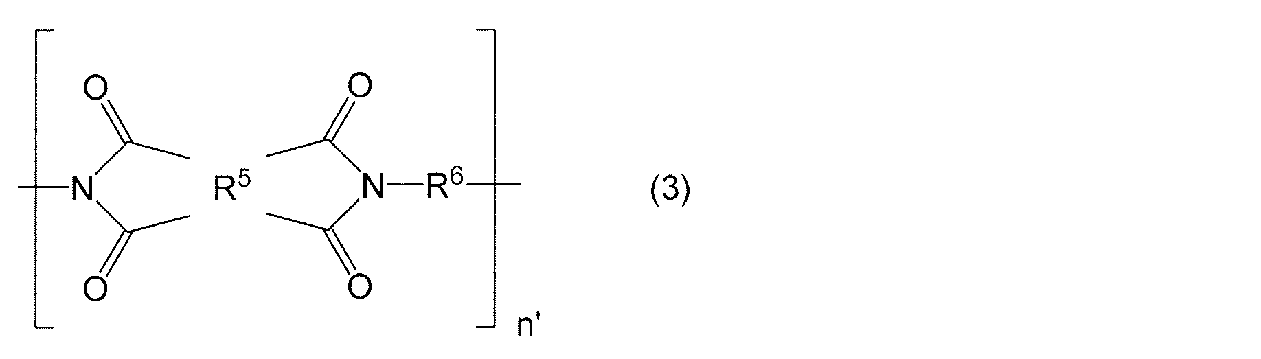
上記一般式(3)において、R5はシクロヘキサンテトラカルボン酸残基、シクロペンタンテトラカルボン酸残基、ジシクロヘキサン-3,4,3’,4’-テトラカルボン酸残基、および4,4'-(ヘキサフルオロイソプロピリデン)ジフタル酸残基からなる群から選ばれる少なくとも1種の4価の基、R6は、ジアミン残基である2価の基を表す。n’は繰り返し単位数を表し、1以上である。 In the general formula (3), R 5 represents a cyclohexanetetracarboxylic acid residue, a cyclopentanetetracarboxylic acid residue, a dicyclohexane-3,4,3 ′, 4′-tetracarboxylic acid residue, and 4,4 ′. At least one tetravalent group selected from the group consisting of-(hexafluoroisopropylidene) diphthalic acid residues, R 6 represents a divalent group that is a diamine residue. n ′ represents the number of repeating units and is 1 or more.
上記一般式(1)における、R1はテトラカルボン酸残基であり、前記例示されたようなテトラカルボン酸二無水物から酸二無水物構造を除いた残基とすることができる。上記一般式(1)におけるR1としては、中でも、光透過性を向上し、かつ剛性を向上する点から、4,4’-(ヘキサフルオロイソプロピリデン)ジフタル酸残基、3,3’,4,4’-ビフェニルテトラカルボン酸残基、ピロメリット酸残基、2,3’,3,4’-ビフェニルテトラカルボン酸残基、3,3’,4,4’-ベンゾフェノンテトラカルボン酸残基、3,3’,4,4’-ジフェニルスルホンテトラカルボン酸残基、4,4'-オキシジフタル酸残基、シクロヘキサンテトラカルボン酸残基、およびシクロペンタンテトラカルボン酸残基からなる群から選択される少なくとも1種を含むことが好ましく、さらに、4,4’-(ヘキサフルオロイソプロピリデン)ジフタル酸残基、4,4’-オキシジフタル酸残基、および3,3’,4,4’-ジフェニルスルホンテトラカルボン酸残基からなる群から選択される少なくとも1種を含むことが好ましい。 In the general formula (1), R 1 is a tetracarboxylic acid residue, and can be a residue obtained by removing the acid dianhydride structure from the tetracarboxylic dianhydride as exemplified above. R 1 in the general formula (1) is, among others, 4,4 ′-(hexafluoroisopropylidene) diphthalic acid residue, 3,3 ′, from the viewpoint of improving light transmittance and improving rigidity. 4,4'-biphenyltetracarboxylic acid residue, pyromellitic acid residue, 2,3 ', 3,4'-biphenyltetracarboxylic acid residue, 3,3', 4,4'-benzophenonetetracarboxylic acid residue Selected from the group consisting of a group, 3,3 ′, 4,4′-diphenylsulfonetetracarboxylic acid residue, 4,4′-oxydiphthalic acid residue, cyclohexanetetracarboxylic acid residue, and cyclopentanetetracarboxylic acid residue At least one selected from the group consisting of 4,4 '-(hexafluoroisopropylidene) diphthalic acid residue, 4,4'-oxydiphthalic acid residue, and 3,3', 4,4'- The It is preferable to include at least one selected from the group consisting of phenylsulfonetetracarboxylic acid residues.
R1において、これらの好適な残基を合計で、50モル%以上含むことが好ましく、更に70モル%以上含むことが好ましく、より更に90モル%以上含むことが好ましい。 In R 1 , these suitable residues are preferably contained in a total amount of 50 mol% or more, more preferably 70 mol% or more, and still more preferably 90 mol% or more.
また、R1として、3,3’,4,4’-ビフェニルテトラカルボン酸残基、3,3’,4,4’-ベンゾフェノンテトラカルボン酸残基、およびピロメリット酸残基からなる群から選択される少なくとも1種のような剛直性を向上するのに適したテトラカルボン酸残基群(グループA)と、4,4’-(ヘキサフルオロイソプロピリデン)ジフタル酸残基、2,3’,3,4’-ビフェニルテトラカルボン酸残基、3,3’,4,4’-ジフェニルスルホンテトラカルボン酸残基、4,4'-オキシジフタル酸残基、シクロヘキサンテトラカルボン酸残基、およびシクロペンタンテトラカルボン酸残基からなる群から選択される少なくとも1種のような透明性を向上するのに適したテトラカルボン酸残基群(グループB)とを混合して用いることも好ましい。 R 1 is selected from the group consisting of 3,3 ′, 4,4′-biphenyltetracarboxylic acid residue, 3,3 ′, 4,4′-benzophenonetetracarboxylic acid residue, and pyromellitic acid residue. A group of tetracarboxylic acid residues (group A) suitable for improving rigidity such as at least one selected from 4,4 ′-(hexafluoroisopropylidene) diphthalic acid residues, 2,3 ′ , 3,4′-biphenyltetracarboxylic acid residue, 3,3 ′, 4,4′-diphenylsulfonetetracarboxylic acid residue, 4,4′-oxydiphthalic acid residue, cyclohexanetetracarboxylic acid residue, and cyclohexane It is also preferable to use a mixture of a tetracarboxylic acid residue group (group B) suitable for improving transparency, such as at least one selected from the group consisting of pentanetetracarboxylic acid residues. There.
この場合、前記剛直性を向上するのに適したテトラカルボン酸残基群(グループA)と、透明性を向上するのに適したテトラカルボン酸残基群(グループB)との含有比率は、透明性を向上するのに適したテトラカルボン酸残基群(グループB)1モルに対して、前記剛直性を向上するのに適したテトラカルボン酸残基群(グループA)が0.05モル以上9モル以下であることが好ましく、更に0.1モル以上5モル以下であることが好ましく、より更に0.3モル以上4モル以下であることが好ましい。 In this case, the content ratio of the tetracarboxylic acid residue group (group A) suitable for improving the rigidity and the tetracarboxylic acid residue group (group B) suitable for improving transparency is, 0.05 mol of the tetracarboxylic acid residue group (group A) suitable for improving the rigidity is 1 mol per 1 mol of the tetracarboxylic acid residue group (group B) suitable for improving the transparency. It is preferably 9 mol or less, more preferably 0.1 mol or more and 5 mol or less, still more preferably 0.3 mol or more and 4 mol or less.
上記一般式(1)におけるR2としては、中でも、光透過性を向上し、かつ剛性を向上する点から、4,4’-ジアミノジフェニルスルホン残基、3,4’-ジアミノジフェニルスルホン残基、および上記一般式(2)で表される2価の基からなる群から選ばれる少なくとも1種の2価の基であることが好ましく、更に、4,4’-ジアミノジフェニルスルホン残基、3,4’-ジアミノジフェニルスルホン残基、ならびに、R3およびR4がパーフルオロアルキル基である上記一般式(2)で表される2価の基からなる群から選ばれる少なくとも1種の2価の基であることが好ましい。 R 2 in the general formula (1) is, among others, 4,4′-diaminodiphenylsulfone residue, 3,4′-diaminodiphenylsulfone residue from the viewpoint of improving light transmittance and improving rigidity. And at least one divalent group selected from the group consisting of a divalent group represented by the general formula (2), and is preferably a 4,4′-diaminodiphenylsulfone residue, 3 , 4′-diaminodiphenylsulfone residue, and at least one divalent group selected from the group consisting of a divalent group represented by the general formula (2) wherein R 3 and R 4 are perfluoroalkyl groups The group is preferably.
上記一般式(3)におけるR5としては、中でも、光透過性を向上し、かつ剛性を向上する点から、4,4'-(ヘキサフルオロイソプロピリデン)ジフタル酸残基、3,3’,4,4’-ジフェニルスルホンテトラカルボン酸残基、及びオキシジフタル酸残基を含むことが好ましい。 R 5 in the general formula (3) is, among others, 4,4 ′-(hexafluoroisopropylidene) diphthalic acid residue, 3,3 ′, from the viewpoint of improving light transmittance and improving rigidity. It preferably contains a 4,4′-diphenylsulfone tetracarboxylic acid residue and an oxydiphthalic acid residue.
R5において、これらの好適な残基を、50モル%以上含むことが好ましく、更に70モル%以上含むことが好ましく、より更に90モル%以上含むことが好ましい。 In R 5 , these suitable residues are preferably contained in an amount of 50 mol% or more, more preferably 70 mol% or more, and even more preferably 90 mol% or more.
上記一般式(3)におけるR6はジアミン残基であり、前記例示されたようなジアミンから2つのアミノ基を除いた残基とすることができる。上記一般式(3)におけるR6としては、中でも、光透過性を向上し、かつ剛性を向上する点から、2,2’-ビス(トリフルオロメチル)ベンジジン残基、ビス[4-(4-アミノフェノキシ)フェニル]スルホン残基、4,4’-ジアミノジフェニルスルホン残基、2,2-ビス[4-(4-アミノフェノキシ)フェニル]ヘキサフルオロプロパン残基、ビス[4-(3-アミノフェノキシ)フェニル]スルホン残基、4,4’-ジアミノ-2,2’-ビス(トリフルオロメチル)ジフェニルエーテル残基、1,4-ビス[4-アミノ-2-(トリフルオロメチル)フェノキシ]ベンゼン残基、2,2-ビス[4-(4-アミノ-2-トリフルオロメチルフェノキシ)フェニル]ヘキサフルオロプロパン残基、4,4’-ジアミノ-2-(トリフルオロメチル)ジフェニルエーテル残基、4,4’-ジアミノベンズアニリド残基、N,N’-ビス(4-アミノフェニル)テレフタルアミド残基、及び9,9-ビス(4-アミノフェニル)フルオレン残基からなる群から選ばれる少なくとも1種の2価の基を含むことが好ましく、更に、2,2’-ビス(トリフルオロメチル)ベンジジン残基、ビス[4-(4-アミノフェノキシ)フェニル]スルホン残基、及び4,4’-ジアミノジフェニルスルホン残基からなる群から選ばれる少なくとも1種の2価の基を含むことが好ましい。 R 6 in the general formula (3) is a diamine residue, and can be a residue obtained by removing two amino groups from the diamine as exemplified above. R6 in the general formula (3) is, among others, a 2,2′-bis (trifluoromethyl) benzidine residue, bis [4- (4- Aminophenoxy) phenyl] sulfone residue, 4,4′-diaminodiphenylsulfone residue, 2,2-bis [4- (4-aminophenoxy) phenyl] hexafluoropropane residue, bis [4- (3-amino Phenoxy) phenyl] sulfone residue, 4,4′-diamino-2,2′-bis (trifluoromethyl) diphenyl ether residue, 1,4-bis [4-amino-2- (trifluoromethyl) phenoxy] benzene Residue, 2,2-bis [4- (4-amino-2-trifluoromethylphenoxy) phenyl] hexafluoropropane residue, 4,4′-diamino-2- (tri Fluoromethyl) diphenyl ether residue, 4,4′-diaminobenzanilide residue, N, N′-bis (4-aminophenyl) terephthalamide residue, and 9,9-bis (4-aminophenyl) fluorene residue It preferably contains at least one divalent group selected from the group consisting of 2,2′-bis (trifluoromethyl) benzidine residue, bis [4- (4-aminophenoxy) phenyl] sulfone residue. The group preferably contains at least one divalent group selected from the group consisting of a group and a 4,4′-diaminodiphenylsulfone residue.
R6において、これらの好適な残基を合計で、50モル%以上含むことが好ましく、更に70モル%以上含むことが好ましく、より更に90モル%以上含むことが好ましい。 In R 6 , these suitable residues are preferably contained in a total amount of 50 mol% or more, more preferably 70 mol% or more, and still more preferably 90 mol% or more.
また、R6として、ビス[4-(4-アミノフェノキシ)フェニル]スルホン残基、4,4’-ジアミノベンズアニリド残基、N,N’-ビス(4-アミノフェニル)テレフタルアミド残基、パラフェニレンジアミン残基、メタフェニレンジアミン残基、および4,4’-ジアミノジフェニルメタン残基からなる群から選択される少なくとも1種のような剛直性を向上するのに適したジアミン残基群(グループC)と、2,2’-ビス(トリフルオロメチル)ベンジジン残基、4,4’-ジアミノジフェニルスルホン残基、2,2-ビス[4-(4-アミノフェノキシ)フェニル]ヘキサフルオロプロパン残基、ビス[4-(3-アミノフェノキシ)フェニル]スルホン残基、4,4’-ジアミノ-2,2’-ビス(トリフルオロメチル)ジフェニルエーテル残基、1,4-ビス[4-アミノ-2-(トリフルオロメチル)フェノキシ]ベンゼン残基、2,2-ビス[4-(4-アミノ-2-トリフルオロメチルフェノキシ)フェニル]ヘキサフルオロプロパン残基、4,4’-ジアミノ-2-(トリフルオロメチル)ジフェニルエーテル残基、及び9,9-ビス(4-アミノフェニル)フルオレン残基からなる群から選択される少なくとも1種のような透明性を向上するのに適したジアミン残基群(グループD)とを混合して用いることも好ましい。 R 6 is a bis [4- (4-aminophenoxy) phenyl] sulfone residue, 4,4′-diaminobenzanilide residue, N, N′-bis (4-aminophenyl) terephthalamide residue, A group of diamine residues suitable for improving the rigidity such as at least one selected from the group consisting of a paraphenylenediamine residue, a metaphenylenediamine residue, and a 4,4′-diaminodiphenylmethane residue (group) C), 2,2′-bis (trifluoromethyl) benzidine residue, 4,4′-diaminodiphenylsulfone residue, 2,2-bis [4- (4-aminophenoxy) phenyl] hexafluoropropane residue Group, bis [4- (3-aminophenoxy) phenyl] sulfone residue, 4,4′-diamino-2,2′-bis (trifluoromethyl) diphenyl Ether residue, 1,4-bis [4-amino-2- (trifluoromethyl) phenoxy] benzene residue, 2,2-bis [4- (4-amino-2-trifluoromethylphenoxy) phenyl] hexa As at least one selected from the group consisting of fluoropropane residues, 4,4′-diamino-2- (trifluoromethyl) diphenyl ether residues, and 9,9-bis (4-aminophenyl) fluorene residues It is also preferable to use a mixture with a diamine residue group (group D) suitable for improving the transparency.
この場合、前記剛直性を向上するのに適したジアミン残基群(グループC)と、透明性を向上するのに適したジアミン残基群(グループD)との含有比率は、透明性を向上するのに適したジアミン残基群(グループD)1モルに対して、前記剛直性を向上するのに適したジアミン残基群(グループC)が0.05モル以上9モル以下であることが好ましく、更に0.1モル以上5モル以下であることが好ましく、0.3モル以上4モル以下であることがより好ましい。 In this case, the content ratio of the diamine residue group (group C) suitable for improving the rigidity and the diamine residue group (group D) suitable for improving transparency improves transparency. The diamine residue group (group C) suitable for improving the rigidity is 0.05 mol or more and 9 mol or less with respect to 1 mol of the diamine residue group (group D) suitable for the treatment. More preferably, it is preferably 0.1 mol or more and 5 mol or less, and more preferably 0.3 mol or more and 4 mol or less.
上記一般式(1)および上記一般式(3)で表される構造において、nおよびn’はそれぞれ独立に、繰り返し単位数を表し、1以上である。ポリイミドにおける繰り返し単位数nは、後述する好ましいガラス転移温度を示すように、構造に応じて適宜選択されれば良く、特に限定されない。平均繰り返し単位数は、通常10~2000であり、更に15~1000であることが好ましい。 In the structures represented by the general formula (1) and the general formula (3), n and n 'each independently represent the number of repeating units and are 1 or more. The number of repeating units n in the polyimide is not particularly limited as long as it is appropriately selected depending on the structure so as to exhibit a preferable glass transition temperature described later. The average number of repeating units is usually 10 to 2000, and more preferably 15 to 1000.
また、ポリイミド系樹脂は、その一部にポリアミド構造を含んでいても良い。含んでいても良いポリアミド構造としては、例えば、トリメリット酸無水物のようなトリカルボン酸残基を含むポリアミドイミド構造や、テレフタル酸のようなジカルボン酸残基を含むポリアミド構造が挙げられる。 Moreover, the polyimide resin may contain a polyamide structure in a part thereof. Examples of the polyamide structure that may be included include a polyamideimide structure containing a tricarboxylic acid residue such as trimellitic anhydride and a polyamide structure containing a dicarboxylic acid residue such as terephthalic acid.
ポリイミド系樹脂は、耐熱性の点から、ガラス転移温度が250℃以上であることが好ましく、更に、270℃以上であることが好ましい。一方、延伸の容易さやベーク温度低減の点から、ガラス転移温度が400℃以下であることが好ましく、更に、380℃以下であることが好ましい。 The polyimide resin preferably has a glass transition temperature of 250 ° C. or higher, and more preferably 270 ° C. or higher, from the viewpoint of heat resistance. On the other hand, the glass transition temperature is preferably 400 ° C. or lower, and more preferably 380 ° C. or lower, from the viewpoint of easy stretching and reduction of the baking temperature.
ポリイミド系樹脂としては、例えば、下記式で表される構造を有する化合物が挙げられる。下記式中、nは、繰り返し単位であり、2以上の整数を表す。
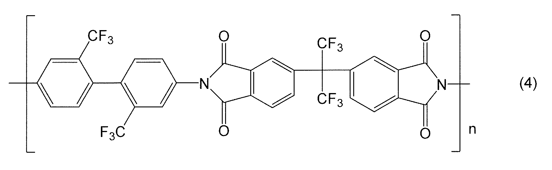
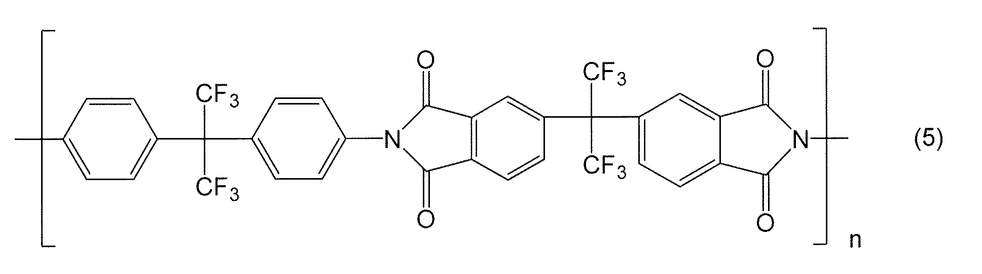
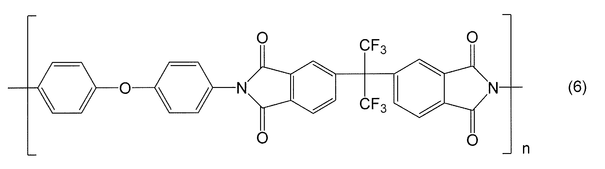
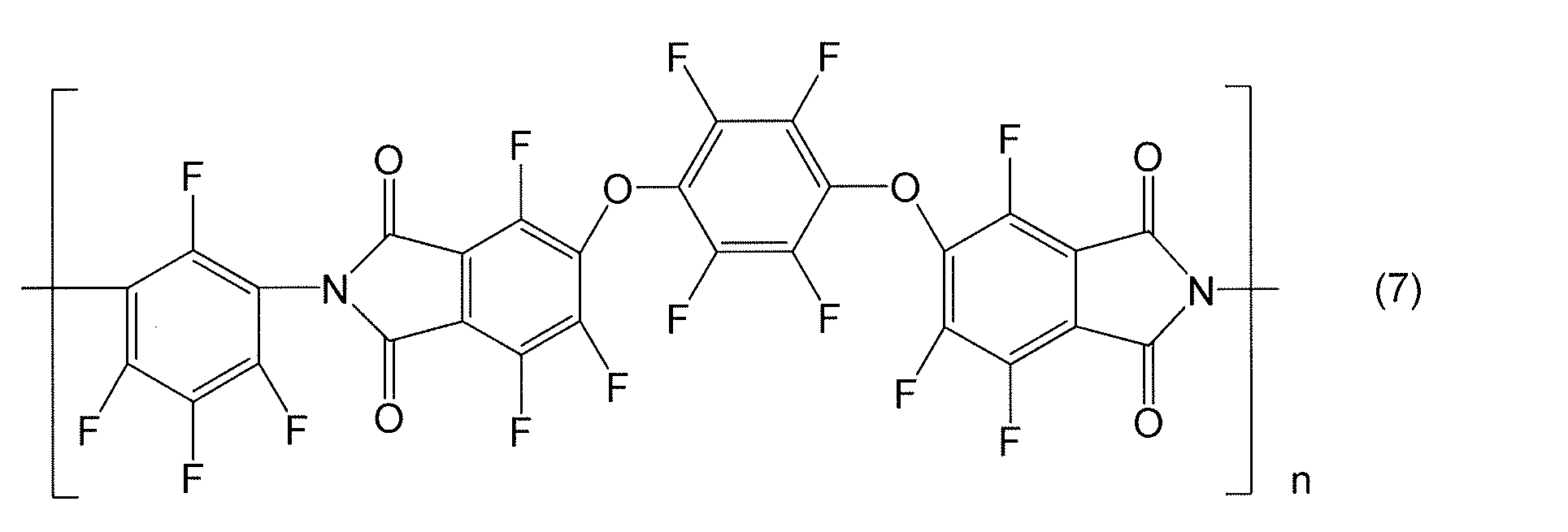
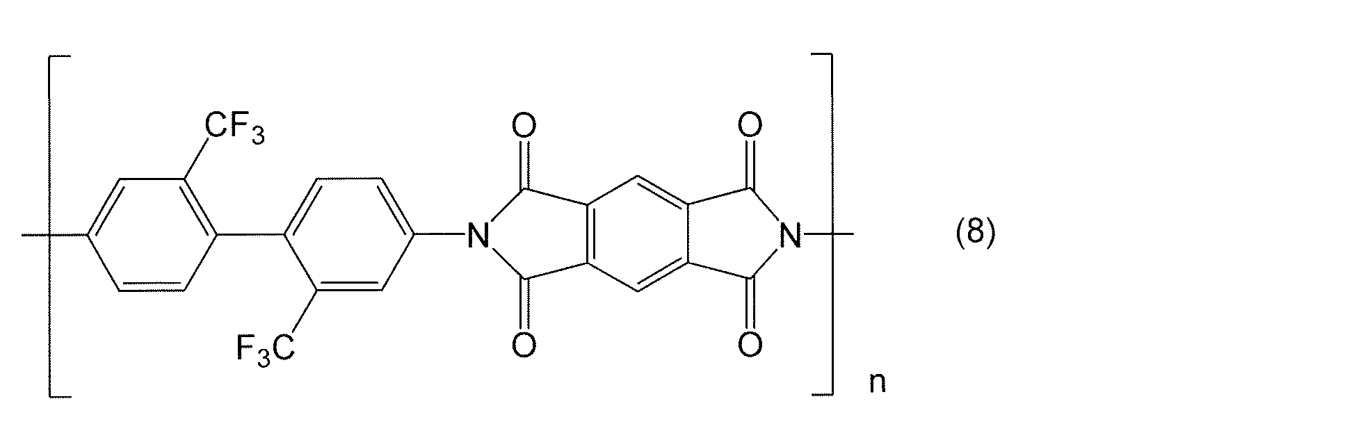
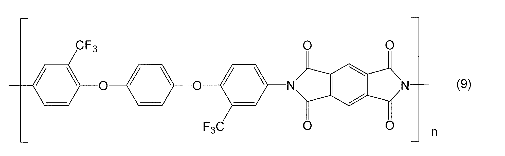

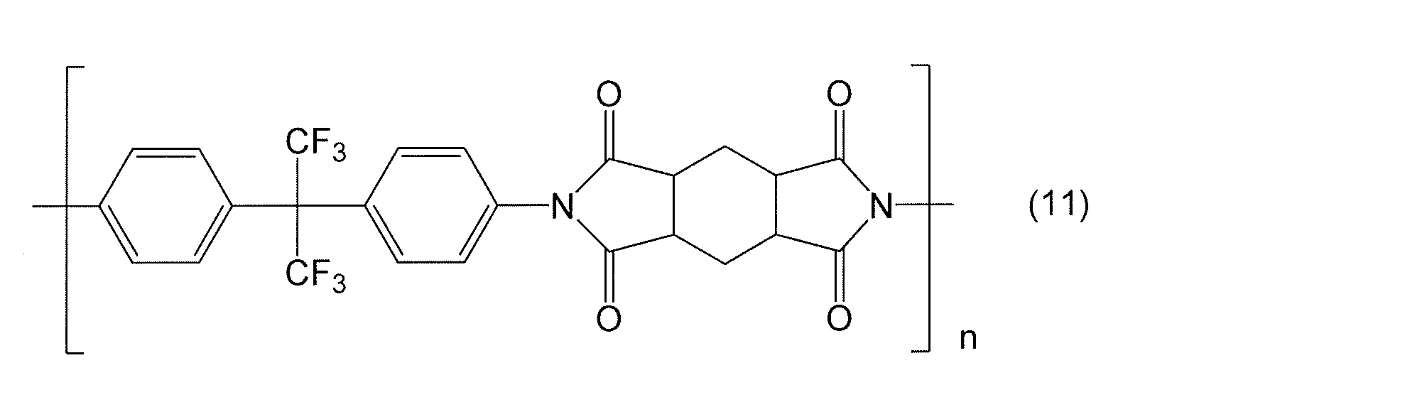


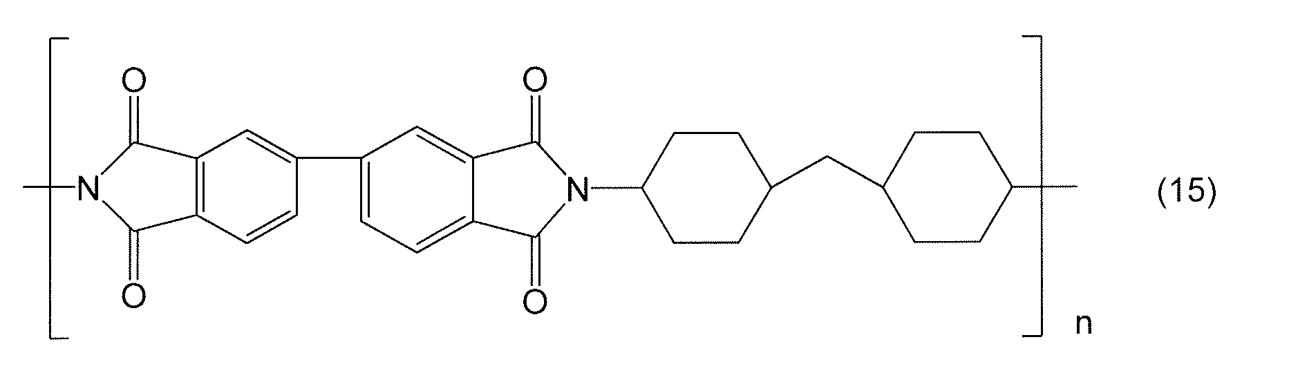
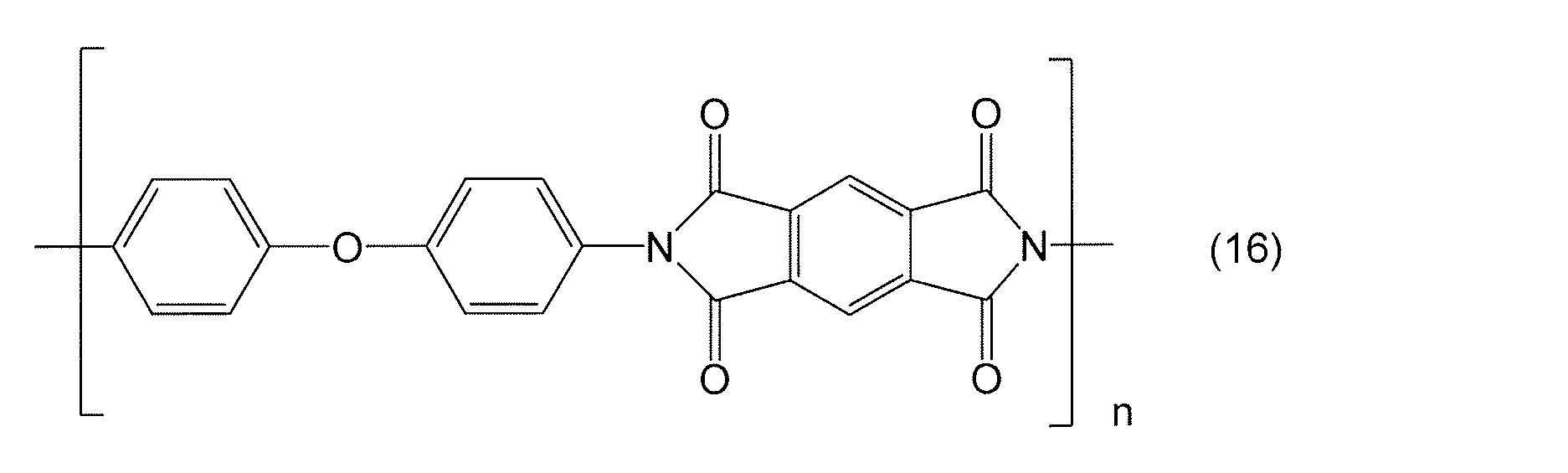


上記ポリイミド系樹脂の中でも、優れた透明性を有することから、分子内又は分子間の電荷移動が起こりにくい構造を有するポリイミド系樹脂またはポリアミド系樹脂が好ましく、具体的には、上記式(4)~(11)等のフッ素化ポリイミド系樹脂、上記式(13)~(16)等の脂環構造を有するポリイミド系樹脂が挙げられる。 Among the polyimide resins, a polyimide resin or a polyamide resin having a structure in which charge transfer within a molecule or between molecules is unlikely to occur is preferable, and specifically, the above formula (4). Fluorinated polyimide resins such as (11) to (11), and polyimide resins having an alicyclic structure such as the above formulas (13) to (16).
また、上記式(4)~(11)等のフッ素化ポリイミド系樹脂では、フッ素化された構造を有するため、高い耐熱性を有しており、ポリイミド系樹脂からなるポリイミドフィルムの製造時の熱によって着色されることもないので、優れた透明性を有する。 In addition, since the fluorinated polyimide resins of the above formulas (4) to (11) have a fluorinated structure, they have high heat resistance, and heat during the production of a polyimide film made of the polyimide resin. Since it is not colored by, it has the outstanding transparency.
ポリアミド系樹脂は、脂肪族ポリアミドのみならず、芳香族ポリアミド(アラミド)を含む概念である。ポリアミド系樹脂としては、例えば、下記式(21)~(23)で表される骨格を有する化合物が挙げられる。なお、下記式中、nは、繰り返し単位であり、2以上の整数を表す。 Polyamide resin is a concept including not only aliphatic polyamide but also aromatic polyamide (aramid). Examples of the polyamide-based resin include compounds having a skeleton represented by the following formulas (21) to (23). In the following formula, n is a repeating unit and represents an integer of 2 or more.
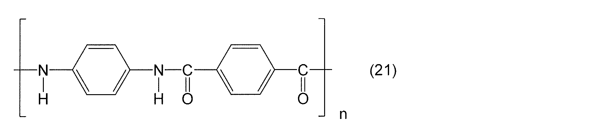

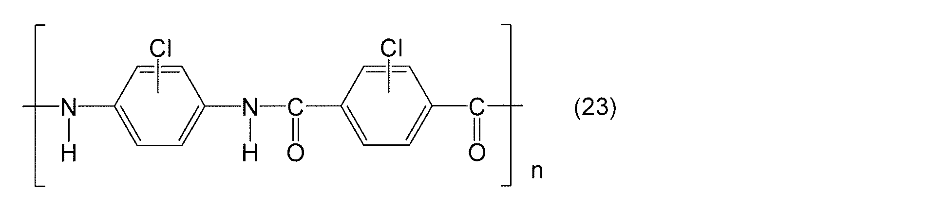
上記式(4)~(20)および(23)で表されるポリイミド系樹脂またはポリアミド系樹脂からなる基材は、市販のものを用いても良い。上記ポリイミド系樹脂からなる基材の市販品としては、例えば、三菱ガス化学社製のネオプリム等が挙げられ、上記ポリアミド系樹脂からなる基材の市販品としては、例えば、東レ社製のミクトロン等が挙げられる。 Commercially available materials may be used as the base material made of the polyimide resin or polyamide resin represented by the above formulas (4) to (20) and (23). Examples of the commercially available base material made of the polyimide-based resin include Neoprim manufactured by Mitsubishi Gas Chemical Co., Ltd., and examples of the commercially available base material made of the polyamide-based resin include Mikutron manufactured by Toray Industries, Inc. Is mentioned.
また、上記式(4)~(20)および(23)で表されるポリイミド系樹脂またはポリアミド系樹脂は、公知の方法により合成したものを用いても良い。例えば、上記式(4)で表されるポリイミド系樹脂の合成方法は、特開2009-132091に記載されており、具体的には、下記式(24)で表される4,4’-ヘキサフルオロプロピリデンビスフタル酸二無水物(FPA)と2,2’-ビス(トリフルオロメチル)-4,4’-ジアミノビフェニル(TFDB)とを反応させることにより得ることができる。
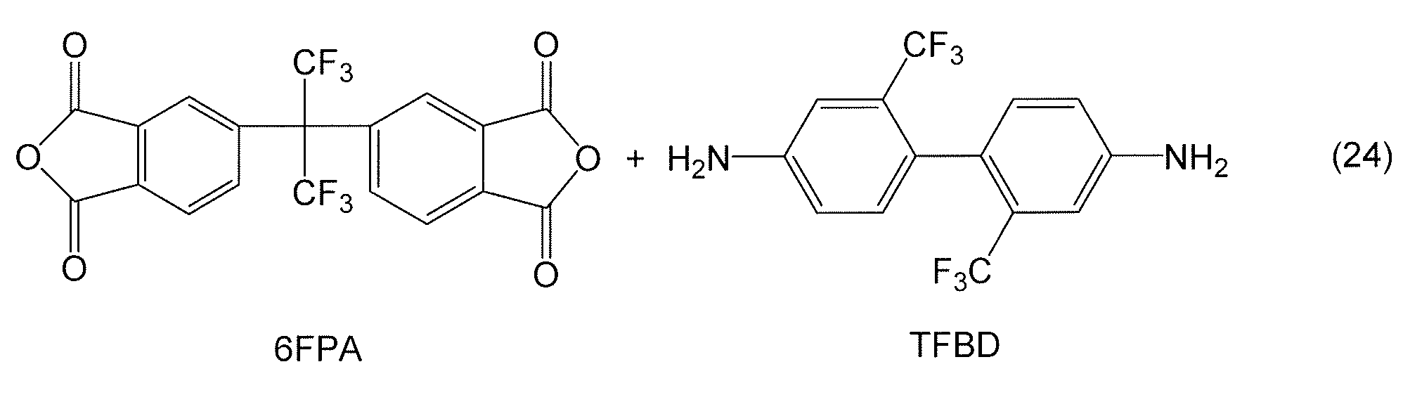
上記ポリイミド系樹脂またはポリアミド系樹脂の重量平均分子量は、3000以上50万以下の範囲であることが好ましく、5000~30万の範囲であることがより好ましく、1万以上20万以下の範囲であることが更に好ましい。重量平均分子量が3000未満であると、充分な強度が得られないことがあり、50万を超えると粘度が上昇し、溶解性が低下するため、表面が平滑で膜厚が均一な基材が得られないことがある。なお、本明細書において、「重量平均分子量」とは、ゲル浸透クロマトグラフィー(GPC)により測定したポリスチレン換算値である。 The weight average molecular weight of the polyimide resin or polyamide resin is preferably in the range of 3000 to 500,000, more preferably in the range of 5000 to 300,000, and in the range of 10,000 to 200,000. More preferably. When the weight average molecular weight is less than 3000, sufficient strength may not be obtained. When the weight average molecular weight exceeds 500,000, the viscosity increases and the solubility decreases, so that a substrate having a smooth surface and a uniform film thickness can be obtained. It may not be obtained. In the present specification, the “weight average molecular weight” is a polystyrene conversion value measured by gel permeation chromatography (GPC).
樹脂基材11は、硬度を向上させることが可能な観点から、上記式(4)~(11)等で表されるフッ素化ポリイミド系樹脂または上記式(23)等のハロゲン基を有するポリアミド系樹脂からなる基材を用いることが好ましい。なかでも、硬度をより向上させることができる観点から、上記式(4)で表されるポリイミド系樹脂からなる基材を用いることがより好ましい。
The
ポリエステル系樹脂としては、例えば、ポリエチレンテレフタレート、ポリプロピレンテレフタレート、ポリブチレンテレフタレート、ポリエチレンナフタレートの少なくとも1種を構成成分とする樹脂等が挙げられる。 Examples of the polyester-based resin include resins having at least one of polyethylene terephthalate, polypropylene terephthalate, polybutylene terephthalate, and polyethylene naphthalate as constituent components.
樹脂基材11の屈折率は、機能層12の屈折率よりも高い。樹脂基材11の屈折率は、例えば、ベッケ法によって測定することができる。樹脂基材11の屈折率をベッケ法を用いて測定する場合、樹脂基材11の欠片を10個切り出し、切り出した10個の欠片において、屈折率標準液を用いて、ベッケ法により屈折率をそれぞれ測定し、測定した欠片の屈折率の10個の平均値を樹脂基材11の屈折率とする。樹脂基材11の屈折率は、1.500以上1.800以下となっていてもよい。また、樹脂基材11の屈折率は、分光光度計(製品名「UV-2450」、島津製作所社製)を用いて、波長380~780nmの平均反射率を測定し、得られた平均反射率を用いて、以下の式(1)によって求めてもよい。樹脂基材11の平均反射率(R)は、裏面反射を防止するために測定スポット面積よりも大きな幅の黒色ビニールテープ(例えば、製品名「ヤマトビニールテープNO200-38-21」、ヤマト社製、38mm幅)を樹脂基材11の裏面に貼り付けてから測定するものとする。
R1=(1-n1)2/(1+n1)2 …(1)
上記式(1)中、R1は波長380~780nmにおける樹脂基材の平均反射率(%)を表し、n1は樹脂基材の屈折率を表す。
The refractive index of the
R 1 = (1-n 1 ) 2 / (1 + n 1) 2 ... (1)
In the above formula (1), R 1 represents the average reflectance (%) of the resin substrate at a wavelength of 380 to 780 nm, and n 1 represents the refractive index of the resin substrate.
樹脂基材11の厚みは、10μm以上100μm以下となっていることが好ましい。樹脂基材の厚みが10μm以上であれば、光学フィルムのカールを抑制でき、また充分な硬度を得ることができ、更に、光学フィルムをRoll to Rollで製造する場合であっても、シワが発生しにくくなり、外観の悪化を招くおそれがない。一方、樹脂基材の厚みが100μm以下であれば、光学フィルムの折り畳み性能が良好であり、連続折り畳み試験の要件を満足させることができ、また、光学フィルムの軽量化の面で好ましい。樹脂基材11の厚みは、走査型電子顕微鏡(SEM)を用いて、樹脂基材11の断面を撮影し、その断面の画像において樹脂基材11の膜厚を10箇所測定し、その10箇所の膜厚の算術平均値とする。樹脂基材11の下限は25μm以上であることがより好ましく、樹脂基材11の上限は80μm以下であることがより好ましい。
The thickness of the
<<機能層>>
機能層12は、ハードコート層として機能する層である。機能層12は、ハードコート性の他、ハードコート性以外の機能を有していてもよい。機能層12は、ハードコート性の他、帯電防止性を有している。すなわち、機能層12は、帯電防止ハードコート層となっている。本明細書における「ハードコート層」とは、ハードコート層の断面中央におけるマルテンス硬度が375MPa以上の層を意味するものとする。本明細書において、「マルテンス硬度」とは、ナノインデンテーション法による硬度測定により、圧子を500nm押込んだときの硬度である。上記ナノインデンテーション法によるマルテンス硬度の測定は、測定サンプルについてHYSITRON(ハイジトロン)社製の「TI950 TriboIndenter」を用いて行うものとする。具体的には、まず、1mm×10mmに切り出した光学フィルムを包埋樹脂によって包埋したブロックを作製し、このブロックから一般的な切片作製方法によって穴等がない均一な、厚さ70nm以上100nm以下の切片を切り出す。切片の作製には、「ウルトラミクロトーム EM UC7」(ライカ マイクロシステムズ株式会社)等を用いることができる。そして、この穴等がない均一な切片が切り出された残りのブロックを測定サンプルとする。次いで、このような測定サンプルにおける上記切片が切り出されることによって得られた断面において、以下の測定条件で、上記圧子としてBerkovich圧子(三角錐)を機能層の断面中央に500nm押し込み、一定保持して残留応力の緩和を行った後、除荷させて、緩和後の最大荷重を計測し、該最大荷重Pmax(μN)と深さ500nmのくぼみ面積A(nm2)とを用い、Pmax/Aにより、マルテンス硬度を算出する。マルテンス硬度は、10箇所測定して得られた値の算術平均値とする。
(測定条件)
・荷重速度:10nm/秒
・保持時間:5秒
・荷重除荷速度:10nm/秒
・測定温度:25℃
<< Functional layer >>
The
(Measurement condition)
・ Loading speed: 10 nm / second ・ Retention time: 5 seconds ・ Load unloading speed: 10 nm / second ・ Measurement temperature: 25 ° C.
機能層12は、機能層12の断面中央におけるマルテンス硬度が500MPa以上2000MPa以下であることが好ましい。機能層12のマルテンス硬度が、500MPa以上であれば、ハードコート層として十分な硬度を得ることができ、また2000MPa以下であれば、良好な光学フィルムの折り畳み性能を得ることができる。機能層12の断面中央におけるマルテンス硬度の下限は600MPa以上であることが好ましく、上限は1500MPa以下であることが好ましい。
The
機能層12の屈折率は、1.400以上1.800以下となっていてもよい。機能層12の屈折率は、分光光度計(製品名「UV-2450」、島津製作所社製)を用いて、波長380~780nmの平均反射率を測定し、得られた平均反射率を用いて、以下の式(2)によって求めることができる。機能層12の平均反射率は、易接着処理が施されていない厚さ50μmのポリエチレンテレフタレート(PET)基材上に機能層用組成物を塗布し、硬化させて1~10μmの厚さの機能層を形成し、PET基材における機能層側の面とは反対側の面(裏面)に、裏面反射を防止するために測定スポット面積よりも大きな幅の黒色ビニールテープ(例えば、製品名「ヤマトビニールテープNO200-38-21」、ヤマト社製、38mm幅)を貼り付けてから測定するものとする。
R2=(1-n2)2/(1+n2)2 …(2)
上記式(2)中、R2は波長380~780nmにおける機能層の平均反射率(%)を表し、n2は機能層の屈折率を表す。
The refractive index of the
R 2 = (1-n 2 ) 2 / (1 + n 2 ) 2 (2)
In the above formula (2), R 2 represents the average reflectance (%) of the functional layer at a wavelength of 380 to 780 nm, and n 2 represents the refractive index of the functional layer.
機能層12の膜厚は、2μm以上40μm以下となっていることが好ましい。機能層12の膜厚が、2μm以上であれば、ハードコート層として十分な硬度を得ることができ、また40μm以下であれば、加工性の悪化を抑制できる。本明細書における「機能層の膜厚」とは、機能層が多層構造となっている場合には、各機能層の膜厚を合計した膜厚(総厚)を意味するものとする。機能層12の上限は30μm以下であることがより好ましく、20μm以下であることがさらに好ましい。
The film thickness of the
機能層12の膜厚は、走査透過型電子顕微鏡(STEM)、または透過型電子顕微鏡(TEM)を用いて、機能層12の断面を撮影し、その断面の画像において機能層12の膜厚を20箇所測定し、その20箇所の膜厚の算術平均値とする。具体的な断面写真の撮影方法を以下に記載する。まず、1mm×10mmの大きさに切り出した光学フィルムを包埋樹脂によって包埋したブロックを作製し、このブロックから一般的な切片作製方法によって穴等がない均一な、厚さ70nm以上100nm以下の切片を切り出す。切片の作製には、「ウルトラミクロトーム EM UC7」(ライカ マイクロシステムズ株式会社)等を用いることができる。そして、この穴等がない均一な切片を測定サンプルとする。その後、走査透過型電子顕微鏡(STEM)(製品名「S-4800」、株式会社日立ハイテクノロジーズ製)を用いて、測定サンプルの断面写真を撮影する。上記S-4800を用いて断面写真を撮影する際には、検出器を「TE」、加速電圧を「30kV」、エミッション電流を「10μA」にして断面観察を行う。倍率については、フォーカスを調節しコントラストおよび明るさを各層が見分けられるか観察しながら5000倍~20万倍で適宜調節する。好ましい倍率は、1万倍~10万倍、更に好ましい倍率は1万倍~5万倍であり、最も好ましい倍率は2.5万倍~5万倍である。なお、上記S-4800を用いて断面写真を撮影する際には、さらに、アパーチャーを「ビームモニタ絞り3」にし、対物レンズ絞りを「3」にし、またW.D.を「8mm」にしてもよい。ハードコート層の膜厚を測定する際には、断面観察した折に、機能層と他の層(例えば、樹脂基材)との界面コントラストが可能な限り明確に観察できることが重要となる。仮に、コントラスト不足でこの界面が見え難い場合には、四酸化オスミウム、四酸化ルテニウム、リンタングステン酸など染色処理を施すと、有機層間の界面が見やすくなるので、染色処理を行ってもよい。また、界面のコントラストは高倍率である方が分かりにくい場合がある。その場合には、低倍率も同時に観察する。例えば、2.5万倍と5万倍や、5万倍と10万倍など、高低の2つの倍率で観察し、両倍率で上記した算術平均値を求め、さらにその平均値を機能層の膜厚の値とする。
The thickness of the
機能層12は、帯電防止ハードコート層となっているので、バインダ樹脂と、バインダ樹脂中に存在する帯電防止剤とを含んでいる。なお、機能層12が、帯電防止性を有しないハードコート層である場合には、帯電防止剤を含んでいなくともよい。また、機能層12は、バインダ樹脂等の他、必要に応じて、本発明の効果を損なわない範囲で、例えば、無機粒子や有機粒子等の粒子、紫外線吸収剤、接着性向上剤、レベリング剤、チクソ性付与剤、カップリング剤、可塑剤、消泡剤、充填剤、着色剤、フィラー等の添加剤を含んでいてもよい。
Since the
<バインダ樹脂>
バインダ樹脂は、重合性化合物(硬化性化合物)の重合体(硬化物)を含む。重合性化合物は、分子内に重合性官能基を少なくとも1つ有するものである。重合性官能基としては、例えば、(メタ)アクリロイル基、ビニル基、アリル基等のエチレン性不飽和基が挙げられる。なお、「(メタ)アクリロイル基」とは、「アクリロイル基」および「メタクリロイル基」の両方を含む意味である。
<Binder resin>
The binder resin contains a polymer (cured product) of a polymerizable compound (curable compound). The polymerizable compound has at least one polymerizable functional group in the molecule. Examples of the polymerizable functional group include ethylenically unsaturated groups such as a (meth) acryloyl group, a vinyl group, and an allyl group. The “(meth) acryloyl group” means to include both “acryloyl group” and “methacryloyl group”.
重合性化合物としては、多官能(メタ)アクリレートが好ましい。上記多官能(メタ)アクリレートとしては、例えば、トリメチロールプロパントリ(メタ)アクリレート、トリプロピレングリコールジ(メタ)アクリレート、ジエチレングリコールジ(メタ)アクリレート、ジプロピレングリコールジ(メタ)アクリレート、ペンタエリスリトールトリ(メタ)アクリレート、ペンタエリスリトールテトラ(メタ)アクリレート、ジペンタエリスリトールヘキサ(メタ)アクリレート、1,6-ヘキサンジオールジ(メタ)アクリレート、ネオペンチルグリコールジ(メタ)アクリレート、トリメチロールプロパントリ(メタ)アクリレート、ジトリメチロールプロパンテトラ(メタ)アクリレート、ジペンタエリスリトールペンタ(メタ)アクリレート、トリペンタエリスリトールオクタ(メタ)アクリレート、テトラペンタエリスリトールデカ(メタ)アクリレート、イソシアヌル酸トリ(メタ)アクリレート、イソシアヌル酸ジ(メタ)アクリレート、ポリエステルトリ(メタ)アクリレート、ポリエステルジ(メタ)アクリレート、ビスフェノールジ(メタ)アクリレート、ジグリセリンテトラ(メタ)アクリレート、アダマンチルジ(メタ)アクリレート、イソボロニルジ(メタ)アクリレート、ジシクロペンタンジ(メタ)アクリレート、トリシクロデカンジ(メタ)アクリレート、ジトリメチロールプロパンテトラ(メタ)アクリレートや、これらをPO、EO、カプロラクトン等で変性したものが挙げられる。 As the polymerizable compound, polyfunctional (meth) acrylate is preferable. Examples of the polyfunctional (meth) acrylate include trimethylolpropane tri (meth) acrylate, tripropylene glycol di (meth) acrylate, diethylene glycol di (meth) acrylate, dipropylene glycol di (meth) acrylate, pentaerythritol tri ( (Meth) acrylate, pentaerythritol tetra (meth) acrylate, dipentaerythritol hexa (meth) acrylate, 1,6-hexanediol di (meth) acrylate, neopentyl glycol di (meth) acrylate, trimethylolpropane tri (meth) acrylate , Ditrimethylolpropane tetra (meth) acrylate, dipentaerythritol penta (meth) acrylate, tripentaerythritol octa (meth) acrylate , Tetrapentaerythritol deca (meth) acrylate, isocyanuric acid tri (meth) acrylate, isocyanuric acid di (meth) acrylate, polyester tri (meth) acrylate, polyester di (meth) acrylate, bisphenol di (meth) acrylate, di Glycerin tetra (meth) acrylate, adamantyl di (meth) acrylate, isobornyl di (meth) acrylate, dicyclopentane di (meth) acrylate, tricyclodecane di (meth) acrylate, ditrimethylolpropane tetra (meth) acrylate, and these Examples thereof include those modified with PO, EO, caprolactone and the like.
これらの中でも上述したマルテンス硬度を好適に満たし得ることから、3~6官能のものが好ましく、例えば、ペンタエリスリトールトリアクリレート(PETA)、ジペンタエリスリトールヘキサアクリレート(DPHA)、ペンタエリスリトールテトラアクリレート(PETTA)、ジペンタエリスリトールペンタアクリレート(DPPA)、トリメチロールプロパントリ(メタ)アクリレート、トリペンタエリスリトールオクタ(メタ)アクリレート、テトラペンタエリスリトールデカ(メタ)アクリレート等が好ましい。なお、本明細書において、「(メタ)アクリレート」とは、「アクリレート」および「メタクリレート」を意味する。 Among them, those having 3 to 6 functional groups are preferable because they can satisfy the above-mentioned Martens hardness, and examples thereof include pentaerythritol triacrylate (PETA), dipentaerythritol hexaacrylate (DPHA), and pentaerythritol tetraacrylate (PETTA). Dipentaerythritol pentaacrylate (DPPA), trimethylolpropane tri (meth) acrylate, tripentaerythritol octa (meth) acrylate, tetrapentaerythritol deca (meth) acrylate, and the like are preferable. In the present specification, “(meth) acrylate” means “acrylate” and “methacrylate”.
なお、硬度や組成物の粘度調整、密着性の改善等のために、更に単官能(メタ)アクリレートモノマーを含んでいてもよい。上記単官能(メタ)アクリレートモノマーとしては、例えば、ヒドロキシエチルアクリレート(HEA)、グリシジルメタクリレート、メトキシポリエチレングリコール(メタ)アクリレート、イソステアリル(メタ)アクリレート、2-アクリロイルオキシエチルサクシネート、アクリロイルモルホリン、N-アクリロイルオキシエチルヘキサヒドロフタルイミド、シクロヘキシルアクリレート、テトラヒドロフリルアクリレート、イソボルニルアクリレート、フェノキシエチルアクリレート、及び、アダマンチルアクリレート等が挙げられる。 In addition, a monofunctional (meth) acrylate monomer may be further included for adjusting the hardness, the viscosity of the composition, improving the adhesion, and the like. Examples of the monofunctional (meth) acrylate monomer include hydroxyethyl acrylate (HEA), glycidyl methacrylate, methoxypolyethylene glycol (meth) acrylate, isostearyl (meth) acrylate, 2-acryloyloxyethyl succinate, acryloylmorpholine, N -Acryloyloxyethyl hexahydrophthalimide, cyclohexyl acrylate, tetrahydrofuryl acrylate, isobornyl acrylate, phenoxyethyl acrylate, adamantyl acrylate and the like.
上記モノマーの重量平均分子量は、機能層の硬度を向上させる観点から、1000未満が好ましく、200以上800以下がより好ましい。また、上記重合性オリゴマーの重量平均分子量は、1000以上2万以下であることが好ましく、1000以上1万以下であることがより好ましく、2000以上7000以下であることが更に好ましい。 The weight average molecular weight of the monomer is preferably less than 1000, more preferably 200 or more and 800 or less, from the viewpoint of improving the hardness of the functional layer. The weight average molecular weight of the polymerizable oligomer is preferably 1000 or more and 20,000 or less, more preferably 1000 or more and 10,000 or less, and further preferably 2000 or more and 7000 or less.
<帯電防止剤>
機能層12に用いられる帯電防止剤は、バインダ樹脂との相溶性が良好であるものであれば、特に限定されない。帯電防止剤としては、イオン伝導型帯電防止剤と電子伝導型帯電防止剤があり、バインダ樹脂との相溶性の観点から、イオン伝導型帯電防止剤が好ましい。
<Antistatic agent>
The antistatic agent used for the
上記イオン伝導型帯電防止剤としては、例えば、第4級アンモニウム塩、ピリジウム塩等のカチオン性帯電防止剤、スルホン酸、リン酸、カルボン酸等のアルカリ金属塩(例えば、リチウム塩、ナトリウム塩、カリウム塩等)等のアニオン性帯電防止剤、アミノ酸系、アミノ酸硫酸エステル系等の両性帯電防止剤、アミノアルコール系、グリセリン系、ポリエチレングリコール系等のノニオン性帯電防止剤等が挙げられる。これらの中でも、バインダ樹脂に対して優れた相溶性を示すことから、第4級アンモニウム塩やリチウム塩が好ましい。 Examples of the ion conduction type antistatic agent include cationic antistatic agents such as quaternary ammonium salts and pyridium salts, and alkali metal salts such as sulfonic acid, phosphoric acid and carboxylic acid (for example, lithium salts, sodium salts, Anionic antistatic agents such as potassium salts), amphoteric antistatic agents such as amino acids and amino acid sulfate esters, and nonionic antistatic agents such as amino alcohols, glycerins, and polyethylene glycols. Among these, quaternary ammonium salts and lithium salts are preferable because they exhibit excellent compatibility with the binder resin.
上記電子伝導型帯電防止剤としては、例えば、ポリアセチレン系、ポリチオフェン系等の導電性ポリマー、金属粒子、金属酸化物粒子等の導電性粒子が挙げられる。これらの中でも、ポリアセチレン、ポリチオフェン等の導電性ポリマーにドーパントを組み合わせた帯電防止剤、金属粒子、金属酸化物粒子が好ましい。また、上記導電性ポリマーに導電性粒子を含有させることもできる。 Examples of the electron conductive antistatic agent include conductive polymers such as polyacetylene-based and polythiophene-based conductive polymers, metal particles, and metal oxide particles. Among these, antistatic agents, metal particles, and metal oxide particles in which a dopant is combined with a conductive polymer such as polyacetylene and polythiophene are preferable. Moreover, electroconductive particle can also be contained in the said electroconductive polymer.
上記導電性ポリマーからなる帯電防止剤としては、具体的には、ポリアセチレン、ポリアニリン、ポリチオフェン、ポリピロール、ポリフェニレンサルファイド、ポリ(1,6-ヘプタジイン)、ポリビフェニレン(ポリパラフェニレン)、ポリパラフィニレンスルフィド、ポリフェニルアセチレン、ポリ(2,5-チエニレン)、又は、これらの誘導体等の導電性高分子が挙げられ、好ましくは、ポリチオフェン系の導電性有機ポリマー(例えば、3,4-エチレンジオキシチオフェン(PEDOT)等)が挙げられる。 Specific examples of the antistatic agent composed of the conductive polymer include polyacetylene, polyaniline, polythiophene, polypyrrole, polyphenylene sulfide, poly (1,6-heptadiyne), polybiphenylene (polyparaphenylene), polyparafinylene sulfide, Examples thereof include conductive polymers such as polyphenylacetylene, poly (2,5-thienylene), and derivatives thereof. Preferably, a polythiophene-based conductive organic polymer (for example, 3,4-ethylenedioxythiophene (for example, PEDOT)).
上記導電性有機ポリマーからなる帯電防止剤を用いることで、湿度依存性が少なく長期間にわたって帯電防止性が維持でき、また、高い透明性、低いヘイズを有し、更に、高いハードコート性、特に鉛筆硬度、スチールウール等に対する耐擦傷性を著しく向上できる。 By using the antistatic agent comprising the conductive organic polymer, the antistatic property can be maintained over a long period of time with little humidity dependency, and also has high transparency, low haze, and high hard coat properties, particularly Pencil hardness and scratch resistance against steel wool can be remarkably improved.
上記金属粒子を構成する金属としては特に限定されず、例えば、Au、Ag、Cu、Al、Fe、Ni、Pd、Pt等の単独、或いはこれら金属の合金が挙げられる。また、上記金属酸化物粒子を構成する金属酸化物としては特に限定されず、例えば、酸化錫(SnO2)、酸化アンチモン(Sb2O5)、アンチモンドープ酸化スズ(ATO)、スズドープ酸化インジウム(ITO)、アルミニウムドープ酸化亜鉛(AZO)、フッ素ドープ酸化スズ(FTO)、酸化亜鉛(ZnO)等が挙げられる。 The metal constituting the metal particles is not particularly limited, and examples thereof include Au, Ag, Cu, Al, Fe, Ni, Pd, and Pt alone or an alloy of these metals. Further, no particular limitation is imposed on the metal oxide constituting the metal oxide particles, for example, tin oxide (SnO 2), antimony oxide (Sb 2 O 5), antimony doped tin oxide (ATO), indium tin oxide ( ITO), aluminum-doped zinc oxide (AZO), fluorine-doped tin oxide (FTO), zinc oxide (ZnO) and the like.
帯電防止剤の含有量としては、特に限定されないが、機能層用組成物の重合性化合物100質量部に対して1質量部以上50質量部以下であることが好ましい。1質量部以上であれば、上述した帯電防止性を充分に得ることができ、50質量部以下であればヘイズ値が小さく、全光線透過率が良好な高透明の膜を得ることができる。上記帯電防止剤の含有量の下限は、10質量部以上であることがより好ましく、上限は40質量部以下であることがより好ましい。 Although it does not specifically limit as content of an antistatic agent, It is preferable that it is 1 to 50 mass parts with respect to 100 mass parts of polymeric compounds of the composition for functional layers. If it is 1 part by mass or more, the above-described antistatic property can be sufficiently obtained, and if it is 50 parts by mass or less, a highly transparent film having a small haze value and good total light transmittance can be obtained. The lower limit of the content of the antistatic agent is more preferably 10 parts by mass or more, and the upper limit is more preferably 40 parts by mass or less.
機能層12は、紫外線吸収剤、分光透過率調整剤、および/または防汚剤をさらに含んでいてもよい。
The
<紫外線吸収剤>
光学フィルムは、折り畳み可能なスマートフォンやタブレット端末のようなモバイル端末に特に好適に用いられるが、このようなモバイル端末は屋外で使用されることが多く、そのため、光学フィルムより表示素子側に配置された偏光子が紫外線に晒されて劣化しやすいという問題がある。しかしながら、機能層12は、偏光子の観察者側に配置されるため、機能層12に紫外線吸収剤が含有されていると、偏光子が紫外線に晒されることによる劣化を好適に防止することができる。なお、上記紫外線吸収剤(UVA)は、機能層12ではなく、樹脂基材11に含有されていてもよい。
<Ultraviolet absorber>
The optical film is particularly preferably used for a mobile terminal such as a foldable smartphone or tablet terminal. However, such a mobile terminal is often used outdoors, and therefore, the optical film is disposed closer to the display element than the optical film. There is a problem that the polarizer is easily deteriorated by being exposed to ultraviolet rays. However, since the
紫外線吸収剤としては、例えば、トリアジン系紫外線吸収剤、ベンゾフェノン系紫外線吸収剤、及び、ベンゾトリアゾール系紫外線吸収剤等が挙げられる。 Examples of ultraviolet absorbers include triazine-based ultraviolet absorbers, benzophenone-based ultraviolet absorbers, and benzotriazole-based ultraviolet absorbers.
上記トリアジン系紫外線吸収剤としては、例えば、2-(2-ヒドロキシ-4-[1-オクチルオキシカルボニルエトキシ]フェニル)-4,6-ビス(4-フェニルフェニル)-1,3,5-トリアジン、2-[4-[(2-ヒドロキシ-3-ドデシルオキシプロピル)オキシ]-2-ヒドロキシフェニル]-4,6-ビス(2,4-ジメチルフェニル)-1,3,5-トリアジン、2,4-ビス[2-ヒドロキシ-4-ブトキシフェニル]-6-(2,4-ジブトキシフェニル)-1,3,5-トリアジン、2-[4-[(2-ヒドロキシ-3-トリデシルオキシプロピル)オキシ]-2-ヒドロキシフェニル]-4,6-ビス(2,4-ジメチルフェニル)-1,3,5-トリアジン、および2-[4-[(2-ヒドロキシ-3-(2’-エチル)ヘキシル)オキシ]-2-ヒドロキシフェニル]-4,6-ビス(2,4-ジメチルフェニル)-1,3,5-トリアジン等が挙げられる。市販されているトリアジン系紫外線吸収剤としては、例えば、TINUVIN460、TINUVIN477(いずれも、BASF社製)、LA-46(ADEKA社製)等が挙げられる。 Examples of the triazine ultraviolet absorber include 2- (2-hydroxy-4- [1-octyloxycarbonylethoxy] phenyl) -4,6-bis (4-phenylphenyl) -1,3,5-triazine. 2- [4-[(2-hydroxy-3-dodecyloxypropyl) oxy] -2-hydroxyphenyl] -4,6-bis (2,4-dimethylphenyl) -1,3,5-triazine, 2 , 4-Bis [2-hydroxy-4-butoxyphenyl] -6- (2,4-dibutoxyphenyl) -1,3,5-triazine, 2- [4-[(2-hydroxy-3-tridecyl) Oxypropyl) oxy] -2-hydroxyphenyl] -4,6-bis (2,4-dimethylphenyl) -1,3,5-triazine, and 2- [4-[(2-hydroxy-3- ( '- ethyl) hexyl) oxy] -2-hydroxyphenyl] -4,6-bis (2,4-dimethylphenyl) -1,3,5-triazine. Examples of commercially available triazine ultraviolet absorbers include TINUVIN 460, TINUVIN 477 (both manufactured by BASF), LA-46 (manufactured by ADEKA), and the like.
上記ベンゾフェノン系紫外線吸収剤としては、例えば、2-ヒドロキシベンゾフェノン、2,4-ジヒドロキシベンゾフェノン、2,2’-ジヒドロキシ-4,4’-ジメトキシベンゾフェノン、2,2’,4,4’-テトラヒドロキシベンゾフェノン、2-ヒドロキシ-4-メトキシベンゾフェノン、ヒドロキシメトキシベンゾフェノンスルホン酸及びその三水塩、ヒドロキシメトキシベンゾフェノンスルホン酸ナトリウム等が挙げられる。市販されているベンゾフェノン系紫外線吸収剤としては、例えば、CHMASSORB81/FL(BASF社製)等が挙げられる。 Examples of the benzophenone ultraviolet absorber include 2-hydroxybenzophenone, 2,4-dihydroxybenzophenone, 2,2′-dihydroxy-4,4′-dimethoxybenzophenone, 2,2 ′, 4,4′-tetrahydroxy. Examples thereof include benzophenone, 2-hydroxy-4-methoxybenzophenone, hydroxymethoxybenzophenone sulfonic acid and its trihydrate, hydroxymethoxybenzophenone sulfonate sodium, and the like. Examples of commercially available benzophenone ultraviolet absorbers include CHMASSORB81 / FL (manufactured by BASF).
上記ベンゾトリアゾール系紫外線吸収剤としては、例えば、2-エチルヘキシル-3-〔3-tert-ブチル-4-ヒドロキシ-5-(5-クロロ-2H-ベンゾトリアゾール-2-イル)フェニル〕プロピオネート、2-(2H-ベンゾトリアゾール-2-イル)-6-(直鎖及び側鎖ドデシル)-4-メチルフェノール、2-〔5-クロロ(2H)-ベンゾトリアゾール-2-イル〕-4-メチル-6-(tert-ブチル)フェノール、2-(2H-ベンゾトリアゾール-2-イル)-4,6-ジ-tert-ペンチルフェノール、2-(2’-ヒドロキシ-5’-メチルフェニル)ベンゾトリアゾール、2-(2’-ヒドロキシ-3’,5’-ジ-tert-ブチルフェニル)ベンゾトリアゾール、2-(2’-ヒドロキシ-3’-tert-ブチル-5’-メチルフェニル)ベンゾトリアゾール、2-(2’-ヒドロキシ-3’,5’-ジ-tert-ブチルフェニル)-5-クロロベンゾトリアゾール、2-(2’-ヒドロキシ-3’-(3’’,4’’,5’’,6’’-テトラヒドロフタルイミドメチル)-5’-メチルフェニル)ベンゾトリアゾール、2,2-メチレンビス(4-(1,1,3,3-テトラメチルブチル)-6-(2H-ベンゾトリアゾール-2-イル)フェノール)、及び、2-(2’-ヒドロキシ-3′-tert-ブチル-5′-メチルフェニル)-5-クロロベンゾトリアゾール等が挙げられる。市販されているベンゾトリアゾール系紫外線吸収剤としては、例えば、KEMISORB71D、KEMISORB79(いずれも、ケミプロ化成社製)、JF-80、JAST-500(いずれも、城北化学社製)、ULS-1933D(一方社製)、RUVA-93(大塚化学社製)等が挙げられる。 Examples of the benzotriazole ultraviolet absorber include 2-ethylhexyl-3- [3-tert-butyl-4-hydroxy-5- (5-chloro-2H-benzotriazol-2-yl) phenyl] propionate, 2 -(2H-benzotriazol-2-yl) -6- (linear and side chain dodecyl) -4-methylphenol, 2- [5-chloro (2H) -benzotriazol-2-yl] -4-methyl- 6- (tert-butyl) phenol, 2- (2H-benzotriazol-2-yl) -4,6-di-tert-pentylphenol, 2- (2′-hydroxy-5′-methylphenyl) benzotriazole, 2- (2′-hydroxy-3 ′, 5′-di-tert-butylphenyl) benzotriazole, 2- (2′-hydroxy-3) -Tert-butyl-5'-methylphenyl) benzotriazole, 2- (2'-hydroxy-3 ', 5'-di-tert-butylphenyl) -5-chlorobenzotriazole, 2- (2'-hydroxy- 3 ′-(3 ″, 4 ″, 5 ″, 6 ″ -tetrahydrophthalimidomethyl) -5′-methylphenyl) benzotriazole, 2,2-methylenebis (4- (1,1,3,3 -Tetramethylbutyl) -6- (2H-benzotriazol-2-yl) phenol) and 2- (2'-hydroxy-3'-tert-butyl-5'-methylphenyl) -5-chlorobenzotriazole Etc. Examples of commercially available benzotriazole ultraviolet absorbers include KEMISORB71D, KEMISORB79 (all manufactured by Chemipro Kasei Co., Ltd.), JF-80, JAST-500 (all manufactured by Johoku Chemical Co., Ltd.), ULS-1933D (one side) And RUVA-93 (manufactured by Otsuka Chemical Co., Ltd.).
紫外線吸収剤は、なかでも、トリアジン系紫外線吸収剤、ベンゾトリアゾール系紫外線吸収剤が好適に用いられる。紫外線吸収剤は、機能層を構成する樹脂成分との溶解性が高いほうが好ましく、また、上述した連続折り畳み試験後のブリードアウトが少ないほうが好ましい。紫外線吸収剤は、ポリマー化又はオリゴマー化されていることが好ましい。紫外線吸収剤としては、ベンゾトリアゾール、トリアジン、ベンゾフェノン骨格を有するポリマー又はオリゴマーが好ましく、具体的には、ベンゾトリアゾールやベンゾフェノン骨格を有する(メタ)アクリレートと、メチルメタクリレート(MMA)とを任意の比率で熱共重合したものであることが好ましい。なお、有機発光ダイオード(OLED)表示装置に光学フィルムを適用する場合、紫外線吸収剤は、OLEDを紫外線から保護する役割も果たすことができる。 Among these, triazine ultraviolet absorbers and benzotriazole ultraviolet absorbers are preferably used as the ultraviolet absorber. It is preferable that the ultraviolet absorber has high solubility with the resin component constituting the functional layer, and it is preferable that the bleedout after the continuous folding test described above is small. The ultraviolet absorber is preferably polymerized or oligomerized. As the ultraviolet absorber, a polymer or oligomer having a benzotriazole, triazine, or benzophenone skeleton is preferable. Specifically, (meth) acrylate having a benzotriazole or benzophenone skeleton and methyl methacrylate (MMA) at an arbitrary ratio. It is preferable that it has been heat copolymerized. In addition, when an optical film is applied to an organic light emitting diode (OLED) display device, the ultraviolet absorber can also serve to protect the OLED from ultraviolet rays.
紫外線吸収剤の含有量としては特に限定されないが、機能層用組成物の固形分100質量部に対して1質量部以上6質量部以下であることが好ましい。1質量部以上であれば、上述した紫外線吸収剤を機能層に含有させる効果を充分に得ることができ、6質量部以下であれば、機能層に著しい着色や強度低下が生じることもない。上記紫外線吸収剤の含有量の下限は2質量部以上であることがより好ましく、上限は5質量部以下であることがより好ましい。 Although it does not specifically limit as content of a ultraviolet absorber, It is preferable that they are 1 mass part or more and 6 mass parts or less with respect to 100 mass parts of solid content of the composition for functional layers. If it is 1 mass part or more, the effect which makes the functional layer contain the ultraviolet absorber mentioned above can fully be acquired, and if it is 6 mass parts or less, remarkable coloring and strength reduction do not occur in the functional layer. As for the minimum of content of the said ultraviolet absorber, it is more preferable that it is 2 mass parts or more, and it is more preferable that an upper limit is 5 mass parts or less.
<分光透過率調整剤>
分光透過率調整剤は、光学フィルムの分光透過率を調整するものである。機能層12に、例えば、下記一般式(25)で表されるセサモール型ベンゾトリアゾール系単量体を含ませた場合には、上述した分光透過率を好適に満たすことができる。

The spectral transmittance adjusting agent adjusts the spectral transmittance of the optical film. For example, when the
上記のセサモール型ベンゾトリアゾール系単量体としては特に制限されないが、具体的な物質名としては、2-[2-(6-ヒドロキシベンゾ[1,3]ジオキソール-5-イル)-2H-ベンゾトリアゾール-5-イル]エチルメタクリレート、2-[2-(6-ヒドロキシベンゾ[1,3]ジオキソール-5-イル)-2H-ベンゾトリアゾール-5-イル]エチルアクリレート、3-[2-(6-ヒドロキシベンゾ[1,3]ジオキソール-5-イル)-2H-ベンゾトリアゾール-5-イル]プロピルメタクリレート、3-[2-(6-ヒドロキシベンゾ[1,3]ジオキソール-5-イル)-2H-ベンゾトリアゾール-5-イル]プロピルアクリレート、4-[2-(6-ヒドロキシベンゾ[1,3]ジオキソール-5-イル)-2H-ベンゾトリアゾール-5-イル]ブチルメタクリレート、4-[2-(6-ヒドロキシベンゾ[1,3]ジオキソール-5-イル)-2H-ベンゾトリアゾール-5-イル]ブチルアクリレート、2-[2-(6-ヒドロキシベンゾ[1,3]ジオキソール-5-イル)-2H-ベンゾトリアゾール-5-イルオキシ]エチルメタクリレート、2-[2-(6-ヒドロキシベンゾ[1,3]ジオキソール-5-イル)-2H-ベンゾトリアゾール-5-イルオキシ]エチルアクリレート、2-[3-{2-(6-ヒドロキシベンゾ[1,3]ジオキソール-5-イル)-2H-ベンゾトリアゾール-5-イル}プロパノイルオキシ]エチルメタクリレート、2-[3-{2-(6-ヒドロキシベンゾ[1,3]ジオキソール-5-イル)-2H-ベンゾトリアゾール-5-イル}プロパノイルオキシ]エチルアクリレート、4-[3-{2-(6-ヒドロキシベンゾ[1,3]ジオキソール-5-イル)-2H-ベンゾトリアゾール-5-イル}プロパノイルオキシ]ブチルメタクリレート、4-[3-{ 2 -(6-ヒドロキシベンゾ[1,3]ジオキソール-5-イル)-2H-ベンゾトリアゾール-5-イル}プロパノイルオキシ]ブチルアクリレート、2-[3-{2-(6-ヒドロキシベンゾ[1,3]ジオキソール-5-イル)-2H-ベンゾトリアゾール-5-イル}プロパノイルオキシ]エチルメタクリレート、2-[3-{2-(6-ヒドロキシベンゾ[1,3]ジオキソール-5-イル)-2H-ベンゾトリアゾール-5-イル}プロパノイルオキシ]エチルアクリレート、2-(メタクリロイルオキシ)エチル2-(6-ヒドロキシベンゾ[1,3]ジオキソール-5-イル)-2H-ベンゾトリアゾール-5カルボキシレート、2-(アクリロイルオキシ)エチル2-(6-ヒドロキシベンゾ[1,3]ジオキソール-5-イル)-2H-ベンゾトリアゾール-5-カルボキシレート、4-(メタクリロイルオキシ)ブチル2-(6-ヒドロキシベンゾ[1,3]ジオキソール-5-イル)-2H-ベンゾトリアゾール-5-カルボキシレート、4-(アクリロイルオキシ)ブチル2-(6-ヒドロキシベンゾ[1,3]ジオキソール-5-イル)-2H-ベンゾトリアゾール-5-カルボキシレート等を挙げることができる。また、これらセサモール型ベンゾトリアゾール系単量体は1種類で用いてもよいし、また2種類以上用いてもよい。 The sesamol type benzotriazole monomer is not particularly limited, but specific substance names include 2- [2- (6-hydroxybenzo [1,3] dioxol-5-yl) -2H-benzo Triazol-5-yl] ethyl methacrylate, 2- [2- (6-hydroxybenzo [1,3] dioxol-5-yl) -2H-benzotriazol-5-yl] ethyl acrylate, 3- [2- (6 -Hydroxybenzo [1,3] dioxol-5-yl) -2H-benzotriazol-5-yl] propyl methacrylate, 3- [2- (6-hydroxybenzo [1,3] dioxol-5-yl) -2H -Benzotriazol-5-yl] propyl acrylate, 4- [2- (6-hydroxybenzo [1,3] dioxol-5-yl -2H-benzotriazol-5-yl] butyl methacrylate, 4- [2- (6-hydroxybenzo [1,3] dioxol-5-yl) -2H-benzotriazol-5-yl] butyl acrylate, 2- [ 2- (6-Hydroxybenzo [1,3] dioxol-5-yl) -2H-benzotriazol-5-yloxy] ethyl methacrylate, 2- [2- (6-hydroxybenzo [1,3] dioxol-5- Yl) -2H-benzotriazol-5-yloxy] ethyl acrylate, 2- [3- {2- (6-hydroxybenzo [1,3] dioxol-5-yl) -2H-benzotriazol-5-yl} prop Noyloxy] ethyl methacrylate, 2- [3- {2- (6-hydroxybenzo [1,3] dioxol-5-yl -2H-benzotriazol-5-yl} propanoyloxy] ethyl acrylate, 4- [3- {2- (6-hydroxybenzo [1,3] dioxol-5-yl) -2H-benzotriazol-5-yl } Propanoyloxy] butyl methacrylate, 4- [3- {2-(6-hydroxybenzo [1,3] dioxol-5-yl) -2H-benzotriazol-5-yl} propanoyloxy] butyl acrylate, 2 -[3- {2- (6-hydroxybenzo [1,3] dioxol-5-yl) -2H-benzotriazol-5-yl} propanoyloxy] ethyl methacrylate, 2- [3- {2- (6 -Hydroxybenzo [1,3] dioxol-5-yl) -2H-benzotriazol-5-yl} propanoyloxy] ethyl acrylate 2- (methacryloyloxy) ethyl 2- (6-hydroxybenzo [1,3] dioxol-5-yl) -2H-benzotriazole-5 carboxylate, 2- (acryloyloxy) ethyl 2- (6- Hydroxybenzo [1,3] dioxol-5-yl) -2H-benzotriazole-5-carboxylate, 4- (methacryloyloxy) butyl 2- (6-hydroxybenzo [1,3] dioxol-5-yl)- 2H-benzotriazole-5-carboxylate, 4- (acryloyloxy) butyl 2- (6-hydroxybenzo [1,3] dioxol-5-yl) -2H-benzotriazole-5-carboxylate, etc. it can. Further, these sesamol type benzotriazole monomers may be used alone or in combination of two or more.
<防汚剤>
防汚剤としては、特に限定されず、例えば、シリコーン系防汚剤、フッ素系防汚剤、シリコーン系かつフッ素系防汚剤が挙げられ、それぞれ単独で使用してもよく、混合して使用してもよい。また、防汚剤としては、アクリル系防汚剤であってもよい。
<Anti-fouling agent>
The antifouling agent is not particularly limited, and examples thereof include silicone antifouling agents, fluorine antifouling agents, silicone type and fluorine antifouling agents, which may be used alone or in combination. May be. The antifouling agent may be an acrylic antifouling agent.
防汚剤の含有量としては、上述した重合性化合物100質量部に対して、0.01~3.0質量部であることが好ましい。0.01質量部以上であれば、機能層に充分な防汚性能を付与でき、また、3.0質量部以下であれば、機能層の硬度が低下するおそれもない。 The content of the antifouling agent is preferably 0.01 to 3.0 parts by mass with respect to 100 parts by mass of the polymerizable compound described above. If it is 0.01 part by mass or more, sufficient antifouling performance can be imparted to the functional layer, and if it is 3.0 parts by mass or less, the hardness of the functional layer does not decrease.
防汚剤は、重量平均分子量が5000以下であることが好ましく、防汚性能の耐久性を改善するために、反応性官能基を好ましくは1以上、より好ましくは2以上有する化合物である。なかでも、2以上の反応性官能基を有する防汚剤を用いることにより、優れた耐擦傷性を付与することができる。 The antifouling agent preferably has a weight average molecular weight of 5000 or less, and is a compound having preferably 1 or more, more preferably 2 or more reactive functional groups in order to improve the durability of the antifouling performance. Among them, excellent scratch resistance can be imparted by using an antifouling agent having two or more reactive functional groups.
防汚剤が反応性官能基を有さない場合、光学フィルムがロール状の場合でも、シート状の場合でも、重ねたときに光学フィルムの裏面に防汚剤が転移してしまい、光学フィルムの裏面に他の層を貼り付けまたは塗布しようとすると、他の層の剥がれ発生することがあり、更に、複数回の連続折り畳み試験を行うことで容易に剥がれる場合がある。 When the antifouling agent does not have a reactive functional group, the antifouling agent is transferred to the back surface of the optical film when it is stacked, whether it is a roll or a sheet. When an attempt is made to attach or apply another layer to the back surface, the other layer may be peeled off and may be easily peeled off by performing a plurality of continuous folding tests.
更に、上記反応性官能基を有する防汚剤は、防汚性能の性能持続性(耐久性)が良好となり、なかでも、上述したフッ素系防汚剤を含む機能層は、指紋が付きにくく(目立ちにくく)、拭き取り性も良好である。更に、機能層用組成物の塗工時の表面張力を下げることができるので、レベリング性がよく、形成する機能層の外観が良好なものとなる。 Furthermore, the antifouling agent having the reactive functional group has good antifouling performance durability (durability), and in particular, the functional layer containing the above-described fluorine-based antifouling agent is difficult to have a fingerprint ( Less noticeable) and good wiping property. Furthermore, since the surface tension at the time of application of the functional layer composition can be lowered, the leveling property is good, and the appearance of the functional layer to be formed is good.
シリコーン系防汚剤を含む機能層は、滑り性がよく、耐スチールウール性が良好である。機能層にこのようなシリコーン系防汚剤を含む光学フィルムを搭載したタッチセンサは、指やペンなどで接触したときの滑りがよくなるため、触感がよくなる。また、機能層に指紋も付きにくく(目立ちにくく)、拭き取り性も良好となる。更に、機能層用組成物の塗工時の表面張力を下げることができるので、レベリング性がよく、形成する機能層の外観が良好なものとなる。 The functional layer containing a silicone-based antifouling agent has good sliding properties and good steel wool resistance. A touch sensor in which an optical film containing such a silicone antifouling agent is mounted on the functional layer has good tactile sensation because of good sliding when touched with a finger or a pen. Further, fingerprints are hardly attached to the functional layer (not easily noticeable), and the wiping property is improved. Furthermore, since the surface tension at the time of application of the functional layer composition can be lowered, the leveling property is good, and the appearance of the functional layer to be formed is good.
シリコーン系防汚剤の市販品としては、例えば、SUA1900L10(新中村化学社製)、SUA1900L6(新中村化学社製)、Ebecryl1360(ダイセルサイテック社製)、UT3971(日本合成社製)、BYKUV3500(ビックケミー社製)、BYKUV3510(ビックケミー社製)、BYKUV3570(ビックケミー社製)、X22-164E、X22-174BX、X22-2426、KBM503、KBM5103(信越化学社製)、TEGO-RAD2250、TEGO-RAD2300、TEGO-RAD2200N、TEGO-RAD2010、TEGO-RAD2500、TEGO-RAD2600、TEGO-RAD2700(エボニックジャパン社製)、メガファックRS854(DIC社製)等が挙げられる。 Examples of commercially available silicone antifouling agents include SUA1900L10 (manufactured by Shin-Nakamura Chemical Co., Ltd.), SUA1900L6 (manufactured by Shin-Nakamura Chemical Co., Ltd.), Ebecryl 1360 (manufactured by Daicel Cytec Co., Ltd.), UT3971 (manufactured by Nippon Gosei Co., Ltd.), and BYKUV3500 (BIC Chemie). BYKUV3510 (by Big Chemie), BYKUV3570 (by Big Chemie), X22-164E, X22-174BX, X22-2426, KBM503, KBM5103 (manufactured by Shin-Etsu Chemical), TEGO-RAD2250, TEGO-RAD2300, TEGO- RAD2200N, TEGO-RAD2010, TEGO-RAD2500, TEGO-RAD2600, TEGO-RAD2700 (manufactured by Evonik Japan), Megafuck RS854 (DIC) Ltd.) and the like.
フッ素系防汚剤の市販品としては、例えば、オプツールDAC、オプツールDSX(ダイキン工業社製)、メガファックRS71、メガファックRS74(DIC社製)、LINC152EPA、LINC151EPA、LINC182UA(共栄社化学社製)、フタージェント650A、フタージェント601AD、フタージェント602等が挙げられる。 Commercially available fluorine-based antifouling agents include, for example, OPTOOL DAC, OPTOOL DSX (manufactured by Daikin Industries, Ltd.), Megafuck RS71, Megafuck RS74 (manufactured by DIC), LINC152EPA, LINC151EPA, and LINC182UA (manufactured by Kyoeisha Chemical Co., Ltd.) Examples of the solvent include 650A, 601ENT, 602, and 602.
フッ素系かつシリコーン系で反応性官能基を有する防汚剤の市販品としては、例えば、メガファックRS851、メガファックRS852、メガファックRS853、メガファックRS854(DIC社製)、オプスターTU2225、オプスターTU2224(JSR社製)、X71-1203M(信越化学社製)等が挙げられる。 Examples of commercially available antifouling agents having fluorine-based and silicone-based reactive functional groups include, for example, MegaFac RS851, MegaFac RS852, MegaFac RS853, MegaFac RS854 (manufactured by DIC), Opstar TU2225, Opstar TU2224 ( JSR), X71-1203M (Shin-Etsu Chemical Co., Ltd.) and the like.
<<第1の光学調整層>>
光学調整層13は、干渉縞の発生を抑制するための層である。光学調整層13の屈折率は、干渉縞の発生を抑制する観点から、樹脂基材11の屈折率よりも低く、かつ機能層12の屈折率よりも高いことが好ましい。光学調整層13の屈折率は、上記機能層の屈折率と同様の方法によって測定することができるので、ここでは説明を省略するものとする。
<< first optical adjustment layer >>
The
光学調整層13と機能層12との屈折率差(光学調整層の屈折率-機能層の屈折率)は、0.005以上0.100以下であることが好ましい。この屈折率差が、0.005以上であれば、光学調整層13と機能層12における界面反射は生じるが干渉縞が視認できないレベルにすることができ、また0.100以下であれば、干渉縞は若干確認されるが、実使用上問題ないレベルにすることができる。この屈折率差の下限は、0.007以上であることがより好ましく、上限は0.090以下であることがより好ましい。光学調整層13の屈折率は、0.010以上0.080以下であってもよい。
The difference in refractive index between the
光学調整層13の膜厚は、30nm以上200nm以下となっていることが好ましい。光学調整層13の膜厚が、30nm以上であれば、機能層12と光学調整層13の充分な密着性を確保でき、また200nm以下であれば、干渉縞をより抑制することができるとともに折り畳み性を向上させることができる。光学調整層13の膜厚は、機能層12と同様の方法によって求めるものとする。光学調整層13の下限は50nm以上であることがより好ましく、上限は150nm以下であることがより好ましい。
The film thickness of the
光学調整層13は、樹脂のみから構成されていてもよいが、バインダ樹脂および屈折率を調整するための粒子を含んでいることが好ましい。光学調整層13のバインダ樹脂は、(メタ)アクリル系樹脂、セルロース系樹脂、ウレタン系樹脂、塩化ビニル系樹脂、ポリエステル系樹脂、ポリオレフィン系樹脂、ポリカーボネート、ナイロン、ポリスチレン、およびABS樹脂からなる群より選択される少なくとも1種の樹脂であることが好ましい。光学調整層13の粒子は、シリカやフッ化マグネシウム等の低屈折率粒子、酸化チタンや酸化ジルコニウム等の金属酸化物粒子、コバルトブルー等の無機顔料等からなる群より選択される少なくとも1種であることが好ましい。これらの中でも、密着性と屈折率差調整の観点から、ポリエステル系樹脂と、酸化チタンや酸化ジルコニウム等の金属酸化物粒子との組み合わせがより好ましい。
The
また、光学調整層13は、帯電防止性を得るために、帯電防止剤を含んでいてもよい。光学調整層13が、帯電防止剤を含んでいる場合、光学調整層13は、帯電防止層としても機能する。光学調整層13が、帯電防止剤を含むことにより、光学フィルム10の表面10Aにおける表面抵抗値をより安定化させることができる。光学調整層13に帯電防止剤を含ませる場合、機能層12にも帯電防止剤を含ませると、光学フィルム10の表面10Aにおける表面抵抗値をさらに安定化させることができる。光学調整層13に含ませる帯電防止剤としては、機能層12の欄で説明した帯電防止剤と同様のものを用いることができるので、ここでは説明を省略するものとする。
The
<<第2の光学調整層>>
光学調整層14は、主に干渉縞を発生させずに樹脂基材11と光学調整層13との間の密着性を向上させるための層である。樹脂基材11と光学調整層13の間に光学調整層14を設けることにより、樹脂基材11と光学調整層13が直接接している場合よりも、密着性を向上させることができる。
<< second optical adjustment layer >>
The
光学調整層14の屈折率は、干渉縞の観点から、樹脂基材11の屈折率よりも低く、かつ光学調整層13の屈折率よりも高いことが好ましい。光学調整層14の屈折率は機能層12と同様の方法によって測定することができるので、ここでは説明省略するものとする。
The refractive index of the
光学調整層14と光学調整層13との屈折率差(第2の光学調整層の屈折率-第1の光学調整層の屈折率)は、0.005以上0.100以下であることが好ましい。この屈折率差が、0.005以上であれば、光学調整層14と光学調整層13における界面反射は生じるが干渉縞が視認できないレベルにすることができ、また0.100以下であれば、干渉縞は若干確認されるが、実使用上問題ないレベルにすることができる。この屈折率差の下限は、0.007以上であることがより好ましく、上限は0.090以下であることがより好ましい。光学調整層13の屈折率は、0.010以上0.080以下であってもよい。
The difference in refractive index between the
光学調整層14の膜厚は、30nm以上200nm以下となっていることが好ましい。光学調整層14の膜厚が、30nm以上であれば、光学調整層13と光学調整層14および樹脂基材11と光学調整層14の充分な密着性を確保でき、また200nm以下であれば、光学調整層14と光学調整層13との屈折率差に起因して、干渉縞が発生することもなく、また折り畳み性を向上させることができる。光学調整層14の膜厚は、機能層12と同様の方法によって求めるものとする。光学調整層14の下限は50nm以上であることがより好ましく、上限は150nm以下であることがより好ましい。
The thickness of the
光学調整層14は、樹脂のみから構成されていてもよいが、バインダ樹脂および屈折率を調整するための粒子を含んでいることが好ましい。光学調整層14の樹脂は、(メタ)アクリル系樹脂、セルロース系樹脂、ウレタン系樹脂、塩化ビニル系樹脂、ポリエステル系樹脂、ポリオレフィン系樹脂、ポリカーボネート、ナイロン、ポリスチレン、およびABS樹脂からなる群より選択される少なくとも1種の樹脂であることが好ましい。光学調整層13の粒子は、シリカやフッ化マグネシウム等の低屈折率粒子、酸化チタンや酸化ジルコニウム等の金属酸化物粒子、コバルトブルー等の無機顔料等からなる群より選択される少なくとも1種であることが好ましい。これらの中でも、密着性と屈折率差調整の観点から、ポリエステル系樹脂と、酸化チタンや酸化ジルコニウム等の金属酸化物粒子との組み合わせがより好ましい。
The
また、光学調整層14は、帯電防止性を得るために、帯電防止剤を含んでいてもよい。光学調整層14が、帯電防止剤を含んでいる場合、光学調整層14は、帯電防止層としても機能する。光学調整層14が、帯電防止剤を含むことにより、光学フィルム10の表面10Aにおける表面抵抗値をより安定化させることができる。光学調整層14に帯電防止剤を含ませる場合、機能層12にも帯電防止剤を含ませると、光学フィルム10の表面10Aにおける表面抵抗値をさらに安定化させることができる。光学調整層14に含ませる帯電防止剤としては、機能層12の欄で説明した帯電防止剤と同様のものを用いることができるので、ここでは説明を省略するものとする。
The
<<第3の光学調整層>>
光学調整層15は、光学フィルム10の光透過率を向上させる層である。光学調整層15の屈折率は、空気の屈折率である1.000より高く、かつ樹脂基材11の屈折率よりも低くなっている。光学調整層15の屈折率は、上記機能層12の屈折率と同様の方法によって測定することができるので、ここでは説明を省略するものとする。
<< Third optical adjustment layer >>
The
樹脂基材11と光学調整層15との屈折率差(樹脂基材の屈折率-第3の光学調整層の屈折率)は、0.005以上0.700以下であることが好ましい。この屈折率差が、0.005以上であれば、光学フィルム10の光透過率を向上させることができ、また0.700以下であれば、光学フィルム10の透明性を損なわない。この屈折率差の下限は、0.010以上であることがより好ましく、上限は0.600以下であることがより好ましい。光学調整層15の屈折率は、0.050以上0.500以下であってもよい。
The difference in refractive index between the
光学調整層15の膜厚は、30nm以上1μm以下となっていることが好ましい。光学調整層15の膜厚が、30nm以上であれば、光学フィルム10の光透過率をより向上させることができ、また1μm以下であれば、加工性の悪化を抑制できる。光学調整層15の膜厚は、機能層12と同様の方法によって求めることができる。光学調整層15の下限は50nm以上であることがより好ましく、上限は700nm以下であることがより好ましく、500nm以下がさらに好ましい。
The film thickness of the
光学調整層15の構成は、屈折率が、1.000より高く、かつ樹脂基材11の屈折率よりも低い層であれば、特に限定されない。光学調整層15は、樹脂から構成することが可能である。光学調整層15は、樹脂の他、さらに屈折率を低下させるために、この樹脂よりも低い屈折率を有する低屈折率粒子を含んでいてもよい。また、光学調整層15は、帯電防止性を得るために、帯電防止剤を含んでいてもよい。光学調整層15が、帯電防止剤を含んでいる場合、光学調整層15は、帯電防止層としても機能する。さらに、光学調整層15は、光学フィルム10の色味を調整するために、上記分光透過率調整剤等の色味調整剤を含んでいてもよい。
The configuration of the
<樹脂>
樹脂は、(メタ)アクリル系樹脂、セルロース系樹脂、ウレタン系樹脂、塩化ビニル系樹脂、ポリエステル系樹脂、ポリオレフィン系樹脂、ポリカーボネート、ナイロン、ポリスチレン、およびABS樹脂からなる群より選択される少なくとも1種の樹脂であることが好ましい。これらの中でも、樹脂基材11との密着性の観点から、(メタ)アクリル系樹脂、ウレタン系樹脂、ポリエステル系樹脂等が好ましい。
<Resin>
The resin is at least one selected from the group consisting of (meth) acrylic resin, cellulose resin, urethane resin, vinyl chloride resin, polyester resin, polyolefin resin, polycarbonate, nylon, polystyrene, and ABS resin. It is preferable that the resin is. Among these, from the viewpoint of adhesion with the
上記(メタ)アクリル系樹脂としては、例えば、ポリメチルメタクリレート等が挙げられる。また、上記セルロース系樹脂としては、例えば、ジアセチルセルロース、セルロースアセテートプロピオネート(CAP)、セルロースアセテートブチレート(CAB)等が挙げられる。上記ウレタン系樹脂としては、例えば、ウレタン樹脂等が挙げられる。 Examples of the (meth) acrylic resin include polymethyl methacrylate. Examples of the cellulose resin include diacetyl cellulose, cellulose acetate propionate (CAP), and cellulose acetate butyrate (CAB). As said urethane type resin, a urethane resin etc. are mentioned, for example.
上記塩化ビニル系樹脂としては、例えば、ポリ塩化ビニル、塩化ビニル-酢酸ビニル共重合体等が挙げられる。また、上記ポリエステル系樹脂としては、例えば、ポリエチレンテレフタレート等が挙げられる。また、上記ポリオレフィン系樹脂としては、例えば、ポリエチレン、ポリプロピレン等が挙げられる。 Examples of the vinyl chloride resin include polyvinyl chloride and vinyl chloride-vinyl acetate copolymers. Moreover, as said polyester-type resin, a polyethylene terephthalate etc. are mentioned, for example. Moreover, as said polyolefin resin, polyethylene, a polypropylene, etc. are mentioned, for example.
<低屈折率粒子>
低屈折率粒子としては、例えば、シリカ、またはフッ化マグネシウムからなる中実または中空粒子等が挙げられる。これらの中でも、中空シリカ粒子が好ましく、このような中空シリカ粒子は、例えば、特開2005-099778号公報の実施例に記載の製造方法にて作製できる。
<Low refractive index particles>
Examples of the low refractive index particles include solid or hollow particles made of silica or magnesium fluoride. Among these, hollow silica particles are preferable, and such hollow silica particles can be produced by, for example, the production method described in Examples in JP-A-2005-099778.
低屈折率粒子の平均粒子径(平均一次粒子径)は、5nm以上100nm以下であることが好ましい。低屈折率粒子の平均粒径が上記範囲内であれば、光学調整層15の透明性を損なうことがなく、良好な粒子の分散状態が得られる。低屈折率粒子の平均粒子径は、透過型電子顕微鏡(TEM)又は走査透過型電子顕微鏡(STEM)を用いて撮影した光学調整層15の断面の画像から20個の低屈折率粒子の粒子径を測定し、20個の低屈折率粒子の粒子径の算術平均値とする。低屈折率粒子の平均粒子径の下限は10nm以上であることがより好ましく、上限は80nm以下がより好ましく、70nm以下がさらに好ましい。
The average particle size (average primary particle size) of the low refractive index particles is preferably 5 nm or more and 100 nm or less. When the average particle diameter of the low refractive index particles is within the above range, the transparency of the
低屈折率粒子としては、表面に反応基を有するシリカ粒子(反応性シリカ粒子)を用いることが好ましく、反応性中空シリカ粒子が特に好ましい。このような表面に反応基を有するシリカ粒子は、シランカップリング剤等によってシリカ粒子を表面処理することによって作成することができる。シリカ粒子の表面をシランカップリング剤で処理する方法としては、シリカ粒子にシランカップリング剤をスプレーする乾式法や、シリカ粒子を溶媒に分散させてからシランカップリング剤を加えて反応させる湿式法等が挙げられる。 As the low refractive index particles, silica particles having reactive groups on the surface (reactive silica particles) are preferably used, and reactive hollow silica particles are particularly preferable. Such silica particles having a reactive group on the surface can be prepared by surface-treating the silica particles with a silane coupling agent or the like. As a method of treating the surface of the silica particles with a silane coupling agent, a dry method in which the silane coupling agent is sprayed on the silica particles, or a wet method in which the silica particles are dispersed in a solvent and then the silane coupling agent is added and reacted. Etc.
<帯電防止剤>
光学調整層15に含有させる帯電防止剤としては、機能層12の欄で説明した帯電防止剤と同様のものを用いることができるので、ここでは説明を省略するものとする。
<Antistatic agent>
As the antistatic agent contained in the
<<光学フィルムの製造方法>>
光学フィルム10は、例えば、以下のようにして作製することができる。まず、樹脂基材11の第1の面11A上に、バーコーター等の塗布装置によって、光学調整層14を形成するための第2の光学調整層用組成物を塗布して、第2の光学調整層用組成物の塗膜を形成する。
<< Optical Film Manufacturing Method >>
The
<第2の光学調整層用組成物>
第2の光学調整層用組成物は、バインダ樹脂前駆体、金属酸化物等の粒子および溶媒を含んでいる。本明細書における「バインダ樹脂前駆体」とは、溶媒を除去することによって、または熱や電離放射線で硬化させることによって、バインダ樹脂となる成分である。バインダ樹脂前駆体としては、溶剤乾燥型樹脂および熱や電離放射線で硬化する重合性化合物が挙げられる。本明細書における電離放射線としては、可視光線、並びに紫外線、X線、電子線、α線、β線、およびγ線が挙げられる。第2の光学調整層用組成物は、その他、必要に応じて、シリカやフッ化マグネシウム等の低屈折率粒子、コバルトブルー等の無機顔料、レベリング剤、および重合開始剤の少なくともいずれかを含んでいてもよい。また、バインダ樹脂前駆体として、ポリエステル系樹脂を用いた場合には、第2の光学調整層用組成物は、その他、必要に応じて、(メタ)アクリル系樹脂、セルロース系樹脂、ウレタン系樹脂、塩化ビニル系樹脂、ポリオレフィン系樹脂、ポリカーボネート、ナイロン、ポリスチレン、ABS樹脂からなる群より選択される1種以上の樹脂を含んでいてもよい。
<Second composition for optical adjustment layer>
The 2nd composition for optical adjustment layers contains particles, such as binder resin precursor and a metal oxide, and a solvent. The “binder resin precursor” in the present specification is a component that becomes a binder resin by removing the solvent or by curing with heat or ionizing radiation. Examples of the binder resin precursor include solvent-drying resins and polymerizable compounds that are cured by heat or ionizing radiation. Examples of the ionizing radiation in this specification include visible light, ultraviolet rays, X-rays, electron beams, α rays, β rays, and γ rays. In addition, the second optical adjustment layer composition contains at least one of low refractive index particles such as silica and magnesium fluoride, inorganic pigments such as cobalt blue, a leveling agent, and a polymerization initiator, if necessary. You may go out. In addition, when a polyester resin is used as the binder resin precursor, the second optical adjustment layer composition may be a (meth) acrylic resin, a cellulose resin, or a urethane resin as necessary. One or more resins selected from the group consisting of vinyl chloride resin, polyolefin resin, polycarbonate, nylon, polystyrene, and ABS resin may be included.
第2の光学調整層用組成物の塗膜を形成した後、各種の公知の方法で塗膜を、例えば40℃以上200℃以下の温度で10秒間~120秒間加熱することにより乾燥させ、溶媒を蒸発させて、または硬化させて、また必要に応じて塗膜に紫外線等の電離放射線を照射して、樹脂基材11に隣接した光学調整層14を形成する。
After forming the coating film of the composition for the second optical adjustment layer, the coating film is dried by, for example, heating at a temperature of 40 ° C. or more and 200 ° C. or less for 10 seconds to 120 seconds by various known methods, Is evaporated or cured, and if necessary, the coating film is irradiated with ionizing radiation such as ultraviolet rays to form the
次いで、光学調整層14上に、バーコーター等の塗布装置によって、光学調整層13を形成するための第1の光学調整層用組成物を塗布して、第1の光学調整層用組成物の塗膜を形成する。
Next, the first optical adjustment layer composition for forming the
<第1の光学調整層用組成物>
第1の光学調整層用組成物は、バインダ樹脂前駆体、金属酸化物等の粒子および溶媒を含んでいる。第1の光学調整層用組成物は、その他、必要に応じて、シリカやフッ化マグネシウム等の低屈折率粒子、コバルトブルー等の無機顔料、レベリング剤、および重合開始剤の少なくともいずれかを含んでいてもよい。また、バインダ樹脂前駆体として、ポリエステル系樹脂を用いた場合には、第1の光学調整層用組成物は、その他、必要に応じて、(メタ)アクリル系樹脂、セルロース系樹脂、ウレタン系樹脂、塩化ビニル系樹脂、ポリオレフィン系樹脂、ポリカーボネート、ナイロン、ポリスチレン、ABS樹脂からなる群より選択される1種以上の樹脂を含んでいてもよい。
<First optical adjustment layer composition>
The 1st composition for optical adjustment layers contains particles, such as a binder resin precursor and a metal oxide, and a solvent. In addition, the first optical adjustment layer composition contains at least one of low refractive index particles such as silica and magnesium fluoride, an inorganic pigment such as cobalt blue, a leveling agent, and a polymerization initiator, if necessary. You may go out. In addition, when a polyester resin is used as the binder resin precursor, the first optical adjustment layer composition may be a (meth) acrylic resin, a cellulose resin, or a urethane resin as necessary. One or more resins selected from the group consisting of vinyl chloride resin, polyolefin resin, polycarbonate, nylon, polystyrene, and ABS resin may be included.
第1の光学調整層用組成物の塗膜を形成した後、各種の公知の方法で塗膜を、例えば40℃以上200℃以下の温度で10秒間~120秒間加熱することにより乾燥させ、溶媒を蒸発させて、または硬化させて、また必要に応じて塗膜に紫外線等の電離放射線を照射して、光学調整層13を形成する。
After forming the coating film of the first optical adjustment layer composition, the coating film is dried by heating at a temperature of, for example, 40 ° C. to 200 ° C. for 10 seconds to 120 seconds by various known methods, The
光学調整層13を形成した後、光学調整層13上に、バーコーター等の塗布装置によって、機能層12を形成するための機能層用組成物を塗布して、機能層用組成物の塗膜を形成する。
After the
<機能層用組成物>
機能層用組成物は、硬化後バインダ樹脂となる重合性化合物を含んでいる。機能層用組成物は、その他、必要に応じて、帯電防止剤、紫外線吸収剤、分光透過率調整剤、防汚剤、無機粒子、レベリング剤、溶媒、重合開始剤を含んでいてもよい。
<Composition for functional layer>
The functional layer composition contains a polymerizable compound that becomes a binder resin after curing. In addition, the functional layer composition may contain an antistatic agent, an ultraviolet absorber, a spectral transmittance adjusting agent, an antifouling agent, inorganic particles, a leveling agent, a solvent, and a polymerization initiator, if necessary.
(溶媒)
上記溶媒としては、アルコール(例、メタノール、エタノール、プロパノール、イソプロパノール、n-ブタノール、s-ブタノール、t-ブタノール、ベンジルアルコール、PGME、エチレングリコール、ジアセトンアルコール)、ケトン(例、アセトン、メチルエチルケトン、メチルイソブチルケトン、シクロペンタノン、シクロヘキサノン、ヘプタノン、ジイソブチルケトン、ジエチルケトン、ジアセトンアルコール)、エステル(酢酸メチル、酢酸エチル、酢酸ブチル、酢酸n-プロピル、酢酸イソプロピル、蟻酸メチル、PGMEA)、脂肪族炭化水素(例、ヘキサン、シクロヘキサン)、ハロゲン化炭化水素(例、メチレンクロライド、クロロホルム、四塩化炭素)、芳香族炭化水素(例、ベンゼン、トルエン、キシレン)、アミド(例、ジメチルホルムアミド、ジメチルアセトアミド、n-メチルピロリドン)、エーテル(例、ジエチルエーテル、ジオキサン、テトラヒドロフラン)、エーテルアルコール(例、1-メトキシ-2-プロパノール)、カーボネート(炭酸ジメチル、炭酸ジエチル、炭酸エチルメチル)、等が挙げられる。これらの溶媒、単独で用いられてもよく、2種類以上が併用されてもよい。なかでも、上記溶媒としては、ウレタン(メタ)アクリレート等の成分、並びに、他の添加剤を溶解或いは分散させ、機能層用組成物を好適に塗工できる点で、メチルイソブチルケトン、メチルエチルケトンが好ましい。
(solvent)
Examples of the solvent include alcohols (eg, methanol, ethanol, propanol, isopropanol, n-butanol, s-butanol, t-butanol, benzyl alcohol, PGME, ethylene glycol, diacetone alcohol), ketones (eg, acetone, methyl ethyl ketone, Methyl isobutyl ketone, cyclopentanone, cyclohexanone, heptanone, diisobutyl ketone, diethyl ketone, diacetone alcohol), ester (methyl acetate, ethyl acetate, butyl acetate, n-propyl acetate, isopropyl acetate, methyl formate, PGMEA), aliphatic Hydrocarbons (eg, hexane, cyclohexane), halogenated hydrocarbons (eg, methylene chloride, chloroform, carbon tetrachloride), aromatic hydrocarbons (eg, benzene, toluene, xylene), Amide (eg, dimethylformamide, dimethylacetamide, n-methylpyrrolidone), ether (eg, diethyl ether, dioxane, tetrahydrofuran), ether alcohol (eg, 1-methoxy-2-propanol), carbonate (dimethyl carbonate, diethyl carbonate, Ethyl methyl carbonate), and the like. These solvents may be used alone or two or more of them may be used in combination. Especially, as said solvent, methyl isobutyl ketone and methyl ethyl ketone are preferable at the point which can dissolve or disperse | distribute components, such as urethane (meth) acrylate, and another additive, and can apply the composition for functional layers suitably. .
(重合開始剤)
重合開始剤は、電離放射線照射より分解されて、ラジカルを発生して重合性化合物の重合(架橋)を開始または進行させる成分である。
(Polymerization initiator)
The polymerization initiator is a component that is decomposed by irradiation with ionizing radiation to generate radicals to initiate or advance polymerization (crosslinking) of the polymerizable compound.
重合開始剤は、電離放射線照射によりラジカル重合を開始させる物質を放出することが可能であれば特に限定されない。重合開始剤としては、特に限定されず、公知のものを用いることができ、具体例には、例えば、アセトフェノン類、ベンゾフェノン類、ミヒラーベンゾイルベンゾエート、α-アミロキシムエステル、チオキサントン類、プロピオフェノン類、ベンジル類、ベンゾイン類、アシルホスフィンオキシド類が挙げられる。また、光増感剤を混合して用いることが好ましく、その具体例としては、例えば、n-ブチルアミン、トリエチルアミン、ポリ-n-ブチルホスフィン等が挙げられる。 The polymerization initiator is not particularly limited as long as it can release a substance that initiates radical polymerization by irradiation with ionizing radiation. The polymerization initiator is not particularly limited, and known ones can be used. Specific examples include, for example, acetophenones, benzophenones, Michler benzoylbenzoate, α-amyloxime ester, thioxanthones, propiophenone. , Benzyls, benzoins, acylphosphine oxides. Further, it is preferable to use a mixture of photosensitizers, and specific examples thereof include n-butylamine, triethylamine, poly-n-butylphosphine and the like.
機能層用組成物の塗膜を形成した後、各種の公知の方法で塗膜を、例えば30℃以上120℃以下の温度で10秒間~120秒間加熱することにより乾燥させ、溶媒を蒸発させる。 After forming the coating film of the functional layer composition, the coating film is dried by heating at a temperature of 30 ° C. or more and 120 ° C. or less for 10 seconds to 120 seconds by various known methods, and the solvent is evaporated.
塗膜を乾燥させた後、塗膜に紫外線等の電離放射線を照射して、塗膜を硬化させる。これにより、光学調整層13に隣接した機能層12が形成される。
After drying the coating film, the coating film is irradiated with ionizing radiation such as ultraviolet rays to cure the coating film. Thereby, the
機能層12を形成した後、樹脂基材11の第2の面11B上に、バーコーター等の塗布装置によって、光学調整層15を形成するための第3の光学調整層用組成物を塗布して、第3の光学調整層用組成物の塗膜を形成する。
After the
<第3の光学調整層用組成物>
第3の光学調整層用組成物は、樹脂前駆体および溶媒を含んでいる。第3の光学調整層用組成物は、その他、必要に応じて、低屈折率粒子、帯電防止剤、コバルトブルー等の無機顔料、レベリング剤、および重合開始剤の少なくともいずれかを含んでいてもよい。また、樹脂前駆体として、ポリエステル系樹脂を用いた場合には、第3の光学調整層用組成物は、その他、必要に応じて、(メタ)アクリル系樹脂、セルロース系樹脂、ウレタン系樹脂、塩化ビニル系樹脂、ポリオレフィン系樹脂、ポリカーボネート、ナイロン、ポリスチレン、ABS樹脂からなる群より選択される1種以上の樹脂を含んでいてもよい。溶媒は、機能層用組成物の欄で説明した溶媒と同様であるので、ここでは説明を省略するものとする。
<Third optical adjustment layer composition>
The 3rd composition for optical adjustment layers contains the resin precursor and the solvent. The third optical adjustment layer composition may further contain at least one of low refractive index particles, an antistatic agent, an inorganic pigment such as cobalt blue, a leveling agent, and a polymerization initiator, if necessary. Good. In addition, when a polyester-based resin is used as the resin precursor, the third optical adjustment layer composition may be a (meth) acrylic resin, a cellulose-based resin, a urethane-based resin, One or more kinds of resins selected from the group consisting of vinyl chloride resin, polyolefin resin, polycarbonate, nylon, polystyrene, and ABS resin may be included. Since the solvent is the same as the solvent described in the column of the functional layer composition, the description is omitted here.
第3の光学調整層用組成物の塗膜を形成した後、各種の公知の方法で塗膜を、例えば40℃以上200℃以下の温度で10秒間~120秒間加熱することにより乾燥させ、溶剤を蒸発させて、または硬化させて、また必要に応じて塗膜に紫外線等の電離放射線を照射して、光学調整層15を形成する。これにより、図1に示される光学フィルム10が得られる。
After forming the coating film of the third optical adjustment layer composition, the coating film is dried by heating at a temperature of, for example, 40 ° C. or more and 200 ° C. or less for 10 seconds to 120 seconds by various known methods, The
<<<他の光学フィルム>>>
光学フィルムは、図4~図7に示される光学フィルム30、40、50、60であってもよい。図4~図7に示される光学フィルム30、40、50、60も、画像表示装置に用いられるものであり、折り畳み可能となっている。
<<< Other optical films >>>
The optical film may be the
図4に示される光学フィルム30は、樹脂基材11と、樹脂基材11の第1の面11A側に設けられた機能層12と、樹脂基材11と機能層12の間に設けられ、機能層12に隣接した光学調整層13とを備えるものである。なお、図4に示される光学フィルム30は、光学調整層14は設けられておらず、光学調整層13は機能層12および樹脂基材11に隣接している。光学フィルム30の物性等は光学フィルム10の物性等と同様であるので、ここでは、説明を省略するものとする。光学フィルム30の表面30Aは、機能層12の表面12Aとなっており、光学フィルム30の裏面30Bは、光学調整層15における樹脂基材11側の面とは反対側の面15Aとなっている。
The
図5に示される光学フィルム40は、樹脂基材11と、樹脂基材11の第1の面11A側に設けられた機能層12と、樹脂基材11と機能層12の間に設けられ、機能層12に隣接した光学調整層13と、樹脂基材11の第2の面11Bに設けられた樹脂層41とを備えるものである。なお、図5に示される光学フィルム40は、光学調整層14は設けられておらず、光学調整層13は機能層12および樹脂基材11に隣接している。光学フィルム40の表面40Aは、機能層12の表面12Aとなっており、光学フィルム40の裏面30Bは、樹脂層41における樹脂基材11側の面とは反対側の面41Aとなっている。
The
図6に示される光学フィルム50は、樹脂基材11と、樹脂基材11の第1の面11A側に設けられた機能層12と、樹脂基材11と機能層12の間に設けられ、機能層12に隣接した光学調整層13と、樹脂基材11の第2の面11B側に設けられた樹脂層41と、樹脂基材11と樹脂層41の間に設けられ、樹脂基材11に隣接した光学調整層15とを備えるものである。なお、図6に示される光学フィルム50は、光学調整層14は設けられておらず、光学調整層13は機能層12および樹脂基材11に隣接している。光学フィルム50の表面50Aは、機能層12の表面12Aとなっており、光学フィルム50の裏面50Bは、樹脂層41における樹脂基材11側の面とは反対側の面41Aとなっている。
The
図7に示される光学フィルム60は、樹脂基材11と、樹脂基材11の第1の面11A側に設けられた機能層12と、樹脂基材11と機能層12の間に設けられ、機能層12に隣接した光学調整層13と、樹脂基材11と光学調整層13の間に設けられ、かつ樹脂基材11に隣接した光学調整層14と、樹脂基材11の第2の面11B側に設けられた樹脂層41と、樹脂基材11と樹脂層41の間に設けられ、樹脂基材11に隣接した光学調整層15とを備えるものである。なお、光学フィルム60の表面60Aは、機能層12の表面12Aとなっており、光学フィルム60の裏面60Bは、樹脂層41における樹脂基材11側の面とは反対側の面41Aとなっている。
The
光学フィルム40、50、60においては、25℃、500Hz以上1000Hz以下の周波数域での剪断貯蔵弾性率G´が、200MPaを超え1200MPa以下となっている。フィルムの剪断貯蔵弾性率G´が200MPaを越えれば、光学フィルムの表面に衝撃が加わった際に、光学フィルム自体の変形のみならず、光学フィルムよりも画像表示装置の内部に粘着層が配置されている場合であっても粘着層の塑性変形を抑制することができる。また、光学フィルム40、50、60の剪断貯蔵弾性率G´が1200MPa以下であれば、折り畳みの際の光学フィルム40の割れを抑制できる。光学フィルム40、50、60の剪断貯蔵弾性率G´の下限は、400MPa以上となっていることが好ましく、500MPa以上となっていることがより好ましい。このような下限とすることで、より優れた耐衝撃性を得ることができる。光学フィルム40、50、60の剪断貯蔵弾性率G´の上限は、800MPa未満となっていることが好ましい。このような上限とすることで、折り畳んで静置し、再び開いた際に、良好な復元性を得ることができる。
In the
光学フィルム40、50、60においては、25℃、500Hz以上1000Hz以下の周波数域での剪断損失弾性率G´´が、3MPa以上150MPa以下となっている。光学フィルムの剪断損失弾性率G´´が3MPa以上であれば、衝撃吸収性能の低下を抑制できる。また、光学フィルム40、50、60の剪断損失弾性率G´´が150MPa以下であれば、樹脂層41の硬度低下を抑制できる。光学フィルム40の剪断損失弾性率G´´の下限は、20MPa以上となっていることが好ましく、また光学フィルム40の剪断損失弾性率G´´の上限は、光学フィルム40、50、60の薄型化の観点から、130MPa以下となっていることが好ましく、100MPa以下となっていることがより好ましい。
In the
剪断貯蔵弾性率G´および剪断損失弾性率G´´は、動的粘弾性測定装置(DMA)によって測定することができる。動的粘弾性測定装置(DMA)によって、光学フィルム40の剪断貯蔵弾性率G´および剪断損失弾性率G´´を測定する際には、まず、光学フィルム40を10mm×5mmの長方形状に打ち抜いて、サンプルを得る。そして、このサンプルを2枚準備し、動的粘弾性測定装置(製品名「Rheogel-E4000」、株式会社ユービーエム社製)のオプションである固体剪断用治具に取り付ける。具体的には、図8に示されるように固体剪断用治具70は、厚さ1mmの1枚の金属製の固体剪断板(中板)と、この固体剪断板71の両側に配置された2つのL型金具72(外板)を備えており、この固体剪断板71と一方のL型金具72との間で一方のサンプルを挟み、かつ固体剪断板71と他方のL型金具72で他方のサンプルを挟む。この場合、樹脂層が固体剪断板51側となり、機能層がL型金具72側となるようにサンプルSを挟む。そして、ビス53でL型金具72間を締めて、サンプルSを固定する。次いで、動的粘弾性測定装置(製品名「Rheogel-E4000」、株式会社ユービーエム社製)に上部チャックおよび下部チャックからなる引張り試験用チャックを取り付けた後、上部チャックと下部チャックの間に固体剪断用治具をチャック間距離20mmで取り付ける。チャック間距離は、上部チャックと下部チャックの間の距離である。そして、設定温度を25℃とし2℃/minで昇温させる。この状態で、固体剪断板71を固定しながら2つのL型金具72に歪み量1%かつ周波数500Hz以上1000Hz以下の範囲の縦振動を与えながら、25℃での固体の動的粘弾性測定を行い、光学フィルム40、50、60の剪断貯蔵弾性率G´および剪断損失弾性率G´´を測定する。ここで、光学フィルムにおける500Hz以上1000Hz以下の周波数域での剪断貯蔵弾性率G´および剪断損失弾性率G´´は、L型金具に周波数500Hz、750Hz、950Hzの縦振動をそれぞれ与えて、それぞれの周波数において光学フィルムの剪断貯蔵弾性率G´および剪断損失弾性率G´´を測定し、これらの剪断貯蔵弾性率G´および剪断損失弾性率G´´の算術平均値を求め、さらに、この測定を3回繰り返し、それぞれ得られた3つの算術平均値をさらに算術平均した値とする。なお、上記において、500Hz以上1000Hz以下の周波数域としたのは、この周波数域の周波数が、数cmの高さから物体を自由落下させたときに、光学フィルムの表面が数ミクロンから数十ミクロン変形する周波数であり、かつ光学フィルムより画像表示装置の内部に存在する表示パネル等に損傷を与える周波数であるからである。
The shear storage elastic modulus G ′ and the shear loss elastic modulus G ″ can be measured by a dynamic viscoelasticity measuring device (DMA). When measuring the shear storage elastic modulus G ′ and the shear loss elastic modulus G ″ of the
光学フィルム40、50、60の物性等は、上記以外は、光学フィルム10の物性等と同様であるので、ここでは、説明を省略するものとする。
Since the physical properties and the like of the
<<樹脂層>>
樹脂層41は、光透過性を有する樹脂からなる層である。樹脂層41は、衝撃吸収性を有する層である。樹脂層は、2以上の樹脂層からなる多層構造となっていてもよい。
<< Resin layer >>
The
樹脂層41の膜厚は、50μm以上300μm以下となっている。樹脂層41の膜厚が、50μm以上であれば、樹脂層41の硬度低下を抑制することができ、また300μm以下であれば、薄型化を図ることができ、かつ加工性が悪化することもない。樹脂層41の膜厚は、走査型電子顕微鏡(SEM)を用いて、樹脂層41の断面を撮影し、その断面の画像において樹脂層41の膜厚を20箇所測定し、その20箇所の膜厚の算術平均値とする。樹脂層41の下限は60μm以上であることがより好ましく、樹脂層41の上限は150μm以下であることがより好ましく、100μm以下であることがさらに好ましい。
The film thickness of the
樹脂層41を構成する樹脂は、光学フィルム40における25℃、500HzHz以上1000Hz以下の周波数域の剪断貯蔵弾性率G´および剪断損失弾性率G´´が上記範囲内となるような樹脂であれば、特に限定されない。このような樹脂としては、アクリル系ゲル、ウレタン系ゲル、シリコーン系ゲル、ウレタン系樹脂、エポキシ系樹脂等が挙げられる。これらの中でも、アクリル系ゲルが好ましい。「ゲル」とは、一般に、高粘度で流動性を失った分散系をいう。なお、樹脂層41は、アクリル系ゲルやウレタン系樹脂等の他、ゴムや熱可塑性エラストマーを含有していてもよい。
The resin constituting the
(アクリル系ゲル)
アクリル系ゲルとしては、粘着剤などに用いられている、アクリル酸エステルを含むモノマーを重合してなるポリマーであれば種々のものを使用することができる。具体的には、アクリル系ゲルとしては、例えば、エチル(メタ)アクリレート、n-プロピル(メタ)アクリレート、i-プロピル(メタ)アクリレート、n-ブチル(メタ)アクリレート、i-ブチル(メタ)アクリレート、2-エチルヘキシル(メタ)アクリレート、n-ヘキシル(メタ)アクリレート、n-アミル(メタ)アクリレート、i-アミル(メタ)アクリレート、オクチル(メタ)アクリレート、i-オクチル(メタ)アクリレート、i-ミリスチル(メタ)アクリレート、ラウリル(メタ)アクリレート、ノニル(メタ)アクリレート、i-ノニル(メタ)アクリレート、i-デシル(メタ)アクリレート、トリデシル(メタ)アクリレート、ステアリル(メタ)アクリレート、i-ステアリル(メタ)アクリレート等のアクリル系モノマーを重合または共重合したものを用いることができる。本明細書において、「(メタ)アクリレート」とは、「アクリレート」および「メタクリレート」の両方を含む意味である。なお、上記(共)重合する際に使用するアクリル酸エステルは、単独で用いる他、2種類以上併用してもよい。
(Acrylic gel)
As the acrylic gel, various polymers can be used as long as they are polymers obtained by polymerizing a monomer containing an acrylate ester used for an adhesive or the like. Specifically, examples of acrylic gels include ethyl (meth) acrylate, n-propyl (meth) acrylate, i-propyl (meth) acrylate, n-butyl (meth) acrylate, and i-butyl (meth) acrylate. 2-ethylhexyl (meth) acrylate, n-hexyl (meth) acrylate, n-amyl (meth) acrylate, i-amyl (meth) acrylate, octyl (meth) acrylate, i-octyl (meth) acrylate, i-myristyl (Meth) acrylate, lauryl (meth) acrylate, nonyl (meth) acrylate, i-nonyl (meth) acrylate, i-decyl (meth) acrylate, tridecyl (meth) acrylate, stearyl (meth) acrylate, i-stearyl (meth) ) Such as acrylate It can be used obtained by polymerizing or copolymerizing acrylic monomers. In the present specification, “(meth) acrylate” means both “acrylate” and “methacrylate”. In addition, the acrylic ester used in the (co) polymerization may be used alone or in combination of two or more.
(ウレタン系樹脂)
ウレタン系樹脂は、ウレタン結合を有する樹脂である。ウレタン系樹脂としては、電離放射線硬化性ウレタン系樹脂組成物の硬化物や熱硬化性ウレタン系樹脂組成物の硬化物等が挙げられる。これらの中でも、高硬度が得られ、硬化速度も早く量産性に優れる観点から、電離放射線硬化性ウレタン系樹脂組成物の硬化物であることが好ましい。
(Urethane resin)
The urethane-based resin is a resin having a urethane bond. Examples of the urethane resin include a cured product of an ionizing radiation curable urethane resin composition and a cured product of a thermosetting urethane resin composition. Among these, a cured product of an ionizing radiation-curable urethane resin composition is preferable from the viewpoint of obtaining high hardness, high curing speed, and excellent mass productivity.
電離放射線硬化性ウレタン系樹脂組成物は、ウレタン(メタ)アクリレートを含んでおり、熱硬化性ウレタン系樹脂は、ポリオール化合物と、イソシアネート化合物とを含んでいる。ウレタン(メタ)アクリレート、ポリオール化合物、およびイソシアネート化合物は、モノマー、オリゴマー、およびプレポリマーのいずれであってもよい。 The ionizing radiation curable urethane-based resin composition includes urethane (meth) acrylate, and the thermosetting urethane-based resin includes a polyol compound and an isocyanate compound. The urethane (meth) acrylate, polyol compound, and isocyanate compound may be any of a monomer, an oligomer, and a prepolymer.
ウレタン(メタ)アクリレート中の(メタ)アクリロイル基の数(官能基数)は、2以上4以下であることが好ましい。ウレタン(メタ)アクリレート中の(メタ)アクリロイル基の数が、2未満であると、鉛筆硬度が低くなるおそれがあり、また4を超えると、硬化収縮が大きくなり、光学フィルムがカールしてしまい、また折り曲げ時に樹脂層にクラックが入るおそれがある。ウレタン(メタ)アクリレート中の(メタ)アクリロイル基の数の上限は、3以下であることがより好ましい。なお、「(メタ)アクリロイル基」とは、「アクリロイル基」および「メタクリロイル基」の両方を含む意味である。 The number of (meth) acryloyl groups (the number of functional groups) in the urethane (meth) acrylate is preferably 2 or more and 4 or less. If the number of (meth) acryloyl groups in the urethane (meth) acrylate is less than 2, the pencil hardness may be lowered, and if it exceeds 4, the curing shrinkage increases and the optical film curls. In addition, there is a risk of cracks in the resin layer during bending. The upper limit of the number of (meth) acryloyl groups in the urethane (meth) acrylate is more preferably 3 or less. The “(meth) acryloyl group” means to include both “acryloyl group” and “methacryloyl group”.
ウレタン(メタ)アクリレートの重量平均分子量は、1500以上20000以下であることが好ましい。ウレタン(メタ)アクリレートの重量平均分子量が、1500未満であると、耐衝撃性が低下するおそれがあり、また20000を超えると、電離放射線硬化性ウレタン系樹脂組成物の粘度が上昇し、塗工性が悪化するおそれがある。ウレタン(メタ)アクリレートの重量平均分子量の下限は2000以上であることがより好ましく、上限は15000以下であることがより好ましい。 The weight average molecular weight of urethane (meth) acrylate is preferably 1500 or more and 20000 or less. If the weight average molecular weight of the urethane (meth) acrylate is less than 1500, the impact resistance may be lowered. If it exceeds 20000, the viscosity of the ionizing radiation-curable urethane resin composition increases, and the coating is applied. May deteriorate. The lower limit of the weight average molecular weight of the urethane (meth) acrylate is more preferably 2000 or more, and the upper limit is more preferably 15000 or less.
また、ウレタン(メタ)アクリレート由来の構造を有する繰り返し単位としては、例えば、下記一般式(26)、(27)、(28)または(29)で表される構造等が挙げられる。
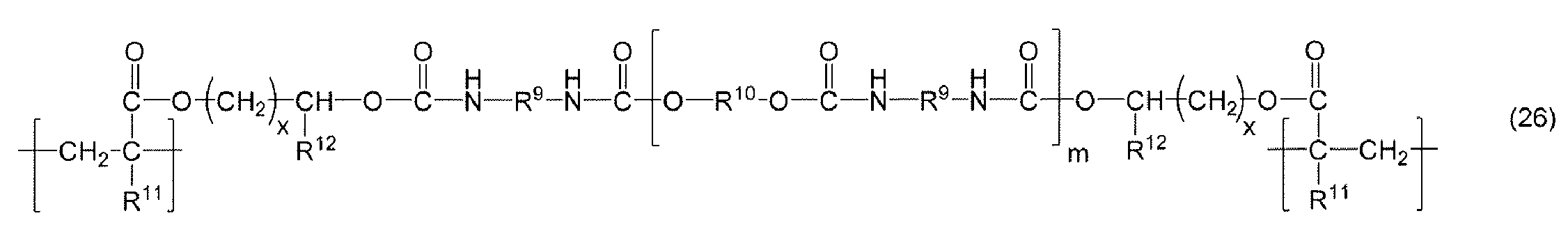


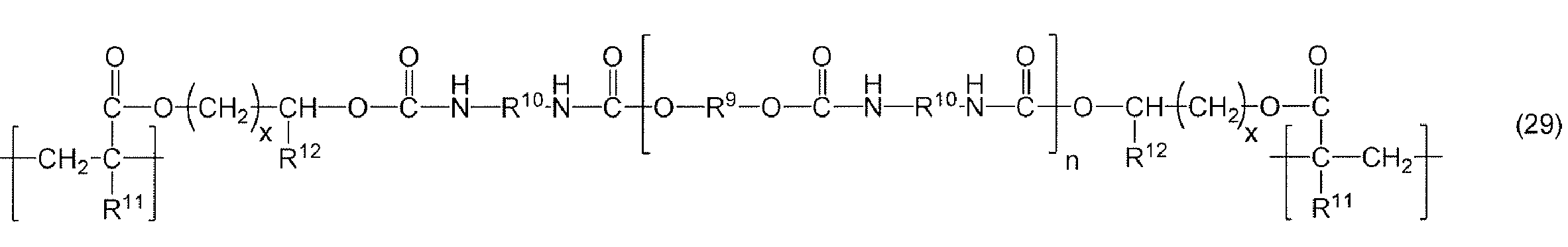
なお、樹脂層41を構成する樹脂が、どのような構造の高分子鎖(繰り返し単位)によって形成されているかは、例えば、熱分解GC-MS及びFT-IRによって樹脂層41を分析することによって判断可能である。特に、熱分解GC-MSは、樹脂層41に含まれる単量体単位をモノマー成分として検知できるため有用である。
It should be noted that the structure of the resin constituting the
樹脂層41は、光学フィルム40、50、60における25℃、500HzHz以上1000Hz以下の周波数域の剪断貯蔵弾性率G´および剪断損失弾性率G´´が上記範囲内となっていれば、紫外線吸収剤、分光透過率調整剤、防汚剤、無機粒子および/または有機粒子等を含んでいてもよい。紫外線吸収剤等は、機能層12の欄で説明した紫外線吸収剤等と同様のものが使用できるので、ここでは説明を省略するものとする。
The
<<<画像表示装置>>>
光学フィルム10、30、40、50、60は、折り畳み可能な画像表示装置に組み込んで使用することが可能である。図9は、本実施形態に係る画像表示装置の概略構成図である。図9に示されるように、画像表示装置80は、観察者側に向けて、主に、電池等が収納された筐体81、保護フィルム82、表示素子83、円偏光板84、タッチセンサ85、および光学フィルム10がこの順で積層されている。表示素子83と円偏光板84との間、円偏光板84とタッチセンサ85との間、タッチセンサ85と光学フィルム10との間には、光透過性を有する粘着層86が配置されており、これら部材は粘着層86によって互いに固定されている。なお、粘着層86は、表示素子83と円偏光板84との間、円偏光板84とタッチセンサ85との間、タッチセンサ85と光学フィルム10との間に配置されているが、粘着層の配置箇所は、光学フィルムと表示素子との間であれば、特に限定されない。
<<< Image display device >>>
The
光学フィルム10は、機能層12が樹脂基材11よりも観察者側となるように配置されている。画像表示装置80においては、光学フィルム10の表面10A(機能層12の表面12A)が、画像表示装置80の表面80Aを構成している。
The
画像表示装置80においては、表示素子83は、有機発光ダイオード等を含む有機発光ダイオード素子となっている。タッチセンサ85は、円偏光板84よりも観察者側に配置されているが、表示素子83と円偏光板84との間に配置されていてもよい。また、タッチセンサ85は、オンセル方式やインセル方式であってもよい。粘着層86としては、例えば、OCA(Optical Clear Adhesive)を用いることができる。
In the
本実施形態によれば、ポリイミド系樹脂、ポリアミドイミド系樹脂、ポリアミド系樹脂、およびポリエステル系樹脂からなる群から選択される1種以上の樹脂からなる樹脂基材11を用い、かつ樹脂基材11と機能層12の間に、機能層12に隣接した光学調整層13を設けているので、折り畳み可能でありながら、干渉縞の発生を抑制することができる。
According to this embodiment, the
光学フィルムの裏面が樹脂基材となっている場合、樹脂基材は空気層と接することになるので、樹脂基材と空気層との界面での反射が大きくなり、これにより光透過率が低下してしまうおそれがある。特に樹脂基材として、ポリイミド系樹脂、ポリアミドイミド系樹脂、ポリアミド系樹脂、およびポリエステル系樹脂からなる群から選択される1種以上の樹脂からなる樹脂基材を用いた場合には、これらの樹脂基材の屈折率は比較的高いので、界面反射が生じやすい。これに対し、本実施形態においては、樹脂基材11の第2の面11Bに、屈折率が1.000より高く、かつ樹脂基材11の屈折率よりも低い光学調整層15を設けているので、樹脂基材が空気層と接しているときと比べて、界面反射を低減させることができ、光反射率を低下させることができる。これにより、光学フィルム10、30の光透過率を向上させることができる。
When the back surface of the optical film is a resin substrate, the resin substrate comes into contact with the air layer, so reflection at the interface between the resin substrate and the air layer increases, thereby reducing light transmittance. There is a risk of it. In particular, when a resin substrate made of one or more resins selected from the group consisting of polyimide resins, polyamideimide resins, polyamide resins, and polyester resins is used as the resin substrate, these resins are used. Since the refractive index of the substrate is relatively high, interface reflection tends to occur. On the other hand, in this embodiment, the
また、光学調整層15が帯電防止剤を含んでいる場合には、光学フィルム10、30、50、60は、樹脂基材11の第1の面11A側に帯電防止ハードコート層である機能層12を備えており、樹脂基材11の第2の面11B側に帯電防止剤を含む光学調整層15を備えているので、光学フィルム10、30、50、60に埃等が付着することが抑制できる。また、この場合には、光学フィルム10、30、50、60の両面に保護フィルム(図示せず)を貼り付けた状態で、光学フィルム10、30、50、60から保護フィルムを剥離したとしても、光学フィルム10、30、50、60の帯電を抑制できる。これにより、画像表示装置の組立工程の歩留まりを向上させることができる。
When the
折り畳み可能な画像表示装置に用いられる光学フィルムには、光学フィルムの表面に衝撃が加わることがあるので、耐衝撃性が求められることがある。ここで、光学フィルムの表面に衝撃が加わったときには、光学フィルムの表面が凹むことがあり、また画像表示装置において光学フィルムよりも内部に存在する表示パネル(例えば、有機発光ダイオードパネル)等の部材が損傷を受けることがある。光学フィルムの表面の凹みに関しては、光学フィルム自体に起因する凹みと、光学フィルムよりも画像表示装置の内部に配置された粘着層のような柔らかい層に起因する凹みがある。「光学フィルム自体に起因する凹み」とは、光学フィルムの表面に衝撃が加わったとき、その衝撃によって光学フィルム自体が変形することによって生じる凹みを意味し、「柔らかい層に起因する凹み」とは、この層が柔らかいために、光学フィルムの表面に衝撃が加わったとき、光学フィルムよりも画像表示装置の内部に配置された柔らかい層が塑性変形を起こし、光学フィルムが柔らかい層の塑性変形に追従することによって生じる凹みを意味する。このため、現在、光学フィルムにおいては、光学フィルムの表面に衝撃が加わったときに、光学フィルム自体に起因する凹みおよび柔らかい層に起因する凹みが抑制され、かつ光学フィルムよりも画像表示装置の内部に存在する部材が損傷を受けないような優れた耐衝撃性が得られることが好ましい。ここで、衝撃吸収性能を表す指標としては、従来から剪断損失正接tanδが知られている。したがって、樹脂基材の第1の面側に機能層および第2の面側に樹脂層を備える構造の光学フィルムにおける耐衝撃性を剪断損失正接tanδで表すことも考えられるが、剪断損失正接tanδでは、光学フィルムの表面(機能層の表面)に衝撃を加えたときに、光学フィルム自体に起因する光学フィルムの表面の凹みおよび柔らかい層に起因する光学フィルムの表面の凹みと、光学フィルムよりも画像表示装置の内部に位置する部材の損傷とを抑制することはできなかった。これは、剪断損失正接tanδが、剪断損失弾性率G´´と剪断貯蔵弾性率G´との比(G´´/G´)であるためであると考えられる。本発明者らが鋭意研究をさらに重ねたところ、光学フィルムの表面に衝撃を加えたときの光学フィルム自体に起因する表面の凹みおよび柔らかい層に起因する表面の凹みと、光学フィルムよりも画像表示装置の内部に位置する部材の損傷とを抑制するためには、樹脂層の膜厚、剪断貯蔵弾性率G´および剪断損失弾性率G´´のバランスが重要であることを見出した。本実施形態によれば、樹脂基材11の第1の面11A側に機能層12および第2の面11B側に樹脂層41を備える構造の光学フィルム40、50、60において、樹脂層41の膜厚が50μm以上300μm以下と薄くなっており、光学フィルム40における上記剪断貯蔵弾性率G´が、200MPaを超え1200MPa以下となっており、かつ光学フィルム40における上記剪損失弾性率G´´が、3MPa以上150MPa以下となっているので、折り畳み可能でありながら、光学フィルム40の表面40Aに衝撃を加えた場合に、光学フィルム40、50、60自体に起因する表面40A、50A、60Aの凹みおよび光学フィルム40、50、60よりも画像表示装置の内部に存在する柔らかい層に起因する光学フィルム40、50、60の表面40A、50A、60Aの凹みを抑制することができるとともに、画像表示装置の内部に位置する表示素子83等の部材の損傷を抑制できる。これにより、優れた耐衝撃性を得ることができる。
Since an optical film used for a foldable image display device may be subjected to an impact on the surface of the optical film, impact resistance may be required. Here, when an impact is applied to the surface of the optical film, the surface of the optical film may be recessed, and a member such as a display panel (for example, an organic light-emitting diode panel) existing inside the optical film in the image display device May be damaged. Regarding the dent on the surface of the optical film, there are a dent resulting from the optical film itself and a dent resulting from a soft layer such as an adhesive layer disposed inside the image display device rather than the optical film. “The dent caused by the optical film itself” means a dent caused by the deformation of the optical film itself due to the impact when an impact is applied to the surface of the optical film. Because the layer is soft, when an impact is applied to the surface of the optical film, the soft layer placed inside the image display device causes plastic deformation rather than the optical film, and the optical film follows the plastic deformation of the soft layer. It means a dent caused by doing. Therefore, at present, in the optical film, when an impact is applied to the surface of the optical film, the dent caused by the optical film itself and the dent caused by the soft layer are suppressed, and the inside of the image display device is more than the optical film. It is preferable that excellent impact resistance is obtained such that a member existing in the substrate is not damaged. Here, the shear loss tangent tan δ is conventionally known as an index representing the impact absorbing performance. Therefore, the impact resistance in an optical film having a structure in which a functional layer is provided on the first surface side of the resin substrate and a resin layer on the second surface side may be expressed as a shear loss tangent tan δ. Then, when an impact is applied to the surface of the optical film (the surface of the functional layer), the dent on the surface of the optical film caused by the optical film itself and the dent on the surface of the optical film caused by the soft layer It was not possible to suppress damage to members located inside the image display device. This is considered to be because the shear loss tangent tan δ is a ratio (G ″ / G ′) between the shear loss elastic modulus G ″ and the shear storage elastic modulus G ′. As a result of further diligent research by the present inventors, the surface dent caused by the optical film itself and the surface dent caused by the soft layer when an impact is applied to the surface of the optical film, and the image display rather than the optical film. In order to suppress damage to members located inside the apparatus, it has been found that the balance of the resin layer thickness, the shear storage elastic modulus G ′, and the shear loss elastic modulus G ″ is important. According to the present embodiment, in the
[第2の実施形態]
以下、本発明の第2の実施形態に係る光学フィルムおよび画像表示装置について、図面を参照しながら説明する。図10は本実施形態に係る光学フィルムの概略構成図であり、図11は本実施形態に係る他の光学フィルムの概略構成図であり、図12は本実施形態に係る画像表示装置の概略構成図である。
[Second Embodiment]
Hereinafter, an optical film and an image display device according to a second embodiment of the present invention will be described with reference to the drawings. FIG. 10 is a schematic configuration diagram of an optical film according to this embodiment, FIG. 11 is a schematic configuration diagram of another optical film according to this embodiment, and FIG. 12 is a schematic configuration of an image display device according to this embodiment. FIG.
<<<光学フィルム>>>
図10に示される光学フィルム90は、画像表示装置に用いられるものであり、折り畳み可能となっている。
<<< Optical film >>>
The
光学フィルム90は、光透過性基材91と、光透過性基材91の一方の面である第1の91A側に設けられた第1の帯電防止層92(以下、単に帯電防止層92と称することもある。)と、光透過性基材91の第1の面91Aとは反対側の面である第2の面91B側に設けられた第2の帯電防止層93(以下、単に帯電防止層93と称することもある。)とを備えるものである。なお、光透過性基材91と帯電防止層92との間および光透過性基材91と帯電防止層93との間の少なくともいずれかに機能層を備えていてもよい。
The
帯電防止層92、93における光透過性基材91側の面とは反対側の面には、保護フィルムが貼り付けられていてもよい。ただし、保護フィルムは使用時に剥離されるものであるので、保護フィルムは、光学フィルムの一部を構成しないものとする。なお、本明細書における光学フィルム90の物性値等は、保護フィルムが設けられていない状態での値である。
A protective film may be attached to the surface of the
図10においては、光学フィルム90の表面90Aは、帯電防止層92の表面92Aとなっている。光学フィルム90の裏面90Bは、帯電防止層93における光透過性基材91側の面とは反対側の面93Aとなっている。
In FIG. 10, the
光学フィルム90は、折り畳み可能となっているが、具体的には、光学フィルム90に対し次に説明する折り畳み試験(連続折り畳み試験)を10万回繰り返し行った場合であっても、光学フィルム90に割れまたは破断が生じないことが好ましく、連続折り畳み試験を20万回繰り返し行った場合であっても、光学フィルム90に割れまたは破断が生じないことがより好ましく、100万回繰り返し行った場合であっても、光学フィルム90に割れまたは破断が生じないことがさらに好ましい。光学フィルム90に対し連続折り畳み試験を10万回繰り返し行った場合に、光学フィルム90に割れ等が生じると、光学フィルム90の折り畳み性が不充分となる。連続折り畳み試験は、帯電防止層92が内側となるように光学フィルム90を折り畳むように行われてもよく、また帯電防止層92が外側となるように光学フィルム90を折り畳むように行われてもよいが、いずれの場合であっても、光学フィルムに割れまたは破断が生じないことが好ましい。連続折り畳み試験は、第1実施形態と同様の方法によって行われるが、本実施形態の連続折り畳み試験では、辺部の間隔を3mmとした状態で行うものとする。
Although the
第1実施形態と同様の方法によって、光学フィルム90に対し70℃で240時間静置する折り畳み静置試験を行った後に折り畳み状態を開放して、室温で30分後に光学フィルム90において開き角θを測定した場合に、光学フィルム90の開き角θが100°以上であることが好ましい。折り畳み静置試験は、帯電防止層92が内側となるように光学フィルム90を折り畳むように行われてもよく、また帯電防止層92が外側となるように光学フィルム90を折り畳むように行われてもよいが、いずれの場合であっても、開き角θが100°以上であることが好ましい。
In the same manner as in the first embodiment, the
光学フィルム90の表面90Aおよび裏面90Bの表面抵抗値は、1012Ω/□以下であることが好ましい。表面抵抗値は、第1実施形態に記載された方法と同様の方法によって測定するものとする。
The surface resistance of the
光学フィルム90の表面90A(帯電防止層92の表面92A)は、JIS K5600-5-4:1999で規定される鉛筆硬度試験で測定されたときの硬度(鉛筆硬度)が、F以上であることが好ましく、2H以上であることがより好ましい。鉛筆硬度試験は、第1実施形態に記載された方法と同様の方法によって測定するものとする。
The
光学フィルム90においては、第1実施形態で記載した理由と同様の理由から、23℃、相対湿度50%の環境下で、光学フィルム90の表面90Aより50mmの距離から10kVの電圧を印加したときの光学フィルム90の表面90Aにおける飽和帯電圧が、0kVを越えていることが好ましい。飽和帯電圧は、第1実施形態に記載された方法と同様の方法によって測定するものとする。上記飽和帯電圧の絶対値の下限は、0.1kV以上であることがより好ましく、上記飽和帯電圧の絶対値の上限は、1.0kV以下であることがより好ましい。
In the
光学フィルム90は、第1実施形態で記載した理由と同様の理由から、イエローインデックス(YI)が15以下であることが好ましい。イエローインデックスは、第1実施形態に記載された方法と同様の方法によって測定するものとする。光学フィルム90のイエローインデックス(YI)の上限は、10未満であることがより好ましく、1.5未満であることが最も好ましい。
The
光学フィルム90に向けて帯電防止層93側から波長300nm以上780nm以下の領域において連続スペクトルを有する光を入射角度0°で照射し、光学フィルム90を透過した光(透過光)におけるL*a*b*表色系の色座標a*、b*を求めたとき、a*が-5以上+5以下であり、b*が-5以上+5以下であることが好ましい。a*およびb*がそれぞれ前記範囲内にあれば、光学フィルムをモバイル端末に用いた場合、画像の黄色味が気にならなくなる。a*およびb*は、第1実施形態に記載された方法と同様の方法によって測定するものとする。
L * a * in the light (transmitted light) transmitted through the
光学フィルム90のヘイズ値(全ヘイズ値)は、第1実施形態で記載した理由と同様の理由から、2.5%以下であることが好ましい。上記ヘイズ値は、第1実施形態に記載された方法と同様の方法によって測定するものとする。上記ヘイズ値は、1.5%以下であることがより好ましく、1.0%以下であることがより好ましい。
The haze value (total haze value) of the
光学フィルム90の波長380nm~780nmの光の視感反射率(反射Y値)は15%以下であることが好ましい。光学フィルムの上記視感反射率が8%以下であれば、光学フィルムをモバイル端末に用いた場合に反射光が少なく視認が容易となる。上記視感反射率は、分光光度計(製品名「UV-2450」、島津製作所社製、光源:タングステンランプおよび重水素ランプ)を用いて、光学フィルムの表面側から波長380nm~780nmの光を照射し、光学フィルムから反射する波長380nm~780nmの光から測定する。具体的には、5cm×10cmの大きさに切り出した光学フィルムの表面側から入射角度5度の光を照射し、光学フィルムで反射された正反射方向の反射光を受光して、380nm~780nmの波長範囲の反射率を測定し、その後、人間が目で感じる明度として換算するソフトウェア(例えば、UV-2450に内蔵されたソフトウェア)によって視感反射率を算出する。上記視感反射率は、10%以下であることがより好ましく、3%以下であることがさらに好ましい。
The luminous reflectance (reflection Y value) of light having a wavelength of 380 nm to 780 nm of the
光学フィルム90におけるその他の物性、用途、および大きさも、光学フィルム10と同様であるので、ここでは、説明を省略するものとする。
Since other physical properties, applications, and sizes of the
<<光透過性基材>>
光透過性基材91は、光透過性を有する樹脂からなる基材である。光透過性基材91の厚みは、第1実施形態に記載した理由と同様の理由から、10μm以上100μm以下となっていることが好ましい。光透過性基材91の厚みは、樹脂基材11の厚みと同様の方法によって測定するものとする。光透過性基材71の下限は25μm以上であることがより好ましく、光透過性基材91の上限は80μm以下であることがより好ましい。
<< light transmissive substrate >>
The
光透過性基材91は、樹脂基材であることが好ましい。樹脂基材を構成する樹脂としては、樹脂基材11と同様の樹脂を用いることができるので、ここでは説明を省略するものとする。
The
<<第1の帯電防止層>>
帯電防止層92は、光学フィルム90の表面90Aに帯電防止性を付与する層である。帯電防止層92は、帯電防止性の他、帯電防止性以外の機能を有していてもよい。帯電防止層92は、帯電防止性の他、ハードコート性を有している。すなわち、帯電防止層92は、帯電防止ハードコート層となっている。帯電防止ハードコート層は、帯電防止性を有するハードコート層である。
<< first antistatic layer >>
The
帯電防止層92は、帯電防止層92の断面中央におけるマルテンス硬度が500MPa以上2000MPa以下であることが好ましい。帯電防止層92のマルテンス硬度が、500MPa以上であれば、帯電防止ハードコート層として十分な硬度を得ることができ、また2000MPa以下であれば、良好な光学フィルムの折り畳み性能を得ることができる。帯電防止層92の断面中央におけるマルテンス硬度の下限は600MPa以上であることが好ましく、上限は1500MPa以下であることが好ましい。帯電防止層92のマルテンス硬度は、第1実施形態に記載された方法と同様の方法によって測定するものとする。
The
帯電防止層92の膜厚は、1μm以上50μm以下となっていることが好ましい。帯電防止層92の膜厚が、1μm以上であれば、帯電防止ハードコート層として十分な硬度を得ることができ、また50μm以下であれば、加工性の悪化を抑制できる。本明細書における「帯電防止層の膜厚」とは、帯電防止層が多層構造となっている場合には、各帯電防止層の膜厚を合計した膜厚(総厚)を意味するものとする。帯電防止層92の膜厚は、機能層12の膜厚と同様の方法によって測定するものとする。帯電防止層92の上限は40μm以下であることがより好ましく、30μm以下であることがさらに好ましい。
The film thickness of the
帯電防止層92は、バインダ樹脂と、バインダ樹脂中に存在する帯電防止剤とを含んでいる。帯電防止層92は、バインダ樹脂等の他、必要に応じて、本発明の効果を損なわない範囲で、例えば、無機粒子や有機粒子等の粒子、紫外線吸収剤、接着性向上剤、レベリング剤、チクソ性付与剤、カップリング剤、可塑剤、消泡剤、充填剤、着色剤、フィラー等の添加剤を含んでいてもよい。
The
<バインダ樹脂>
バインダ樹脂は、機能層12の欄で説明したバインダ樹脂と同様であるので、ここでは説明を省略するものとする。
<Binder resin>
Since the binder resin is the same as the binder resin described in the column of the
<帯電防止剤>
帯電防止剤は、機能層12の欄で説明した帯電防止剤と同様であるので、ここでは説明を省略するものとする。
<Antistatic agent>
Since the antistatic agent is the same as the antistatic agent described in the column of the
帯電防止層92は、紫外線吸収剤、分光透過率調整剤、および/または防汚剤をさらに含んでいてもよい。紫外線吸収剤、分光透過率調整剤および防汚剤は、機能層12の欄で説明した紫外線吸収剤、分光透過率調整剤および防汚剤と同様であるので、ここでは説明を省略するものとする。
The
<<第2の帯電防止層>>
帯電防止層93は、光学フィルム90の裏面90Bに帯電防止性を付与する層である。帯電防止層93の膜厚は、1nm以上0.5μm以下となっていることが好ましい。帯電防止層93の膜厚が、1nm以上であれば、十分な帯電防止性能を得ることができ、また0.5μm以下であれば、加工性の悪化を抑制できる。帯電防止層93の膜厚は、機能層12の膜厚と同様の方法によって測定するものとする。
<< second antistatic layer >>
The
帯電防止層93の膜厚を40nm以上90nm以下とすると、光学フィルム70のイエローインデックスを低下させることができるので、色味調整の観点から、帯電防止層93の膜厚は40nm以上90nm以下であることが好ましい。
If the film thickness of the
帯電防止層93は、帯電防止剤を含んでいる。帯電防止層93は、帯電防止剤の他、バインダ樹脂を含んでいてもよい。
The
<帯電防止剤>
帯電防止層93に含有させる帯電防止剤としては、機能層12の欄で説明した帯電防止剤と同様であるので、ここでは説明を省略するものとする。
<Antistatic agent>
Since the antistatic agent contained in the
<バインダ樹脂>
バインダ樹脂は、(メタ)アクリル系樹脂、セルロース系樹脂、ウレタン系樹脂、塩化ビニル系樹脂、ポリエステル系樹脂、ポリオレフィン系樹脂、ポリカーボネート、ナイロン、ポリスチレン、およびABS樹脂からなる群より選択される少なくとも1種であることが好ましい。これらの中でも、バインダ樹脂の硬度や透明性の観点から、(メタ)アクリル系樹脂、ウレタン系樹脂等が好ましい。
<Binder resin>
The binder resin is at least one selected from the group consisting of (meth) acrylic resin, cellulose resin, urethane resin, vinyl chloride resin, polyester resin, polyolefin resin, polycarbonate, nylon, polystyrene, and ABS resin. Preferably it is a seed. Among these, (meth) acrylic resins and urethane resins are preferable from the viewpoint of the hardness and transparency of the binder resin.
上記(メタ)アクリル系樹脂としては、例えば、ポリメチルメタクリレート等が挙げられる。また、上記セルロース系樹脂としては、例えば、ジアセチルセルロース、セルロースアセテートプロピオネート(CAP)、セルロースアセテートブチレート(CAB)等が挙げられる。上記ウレタン系樹脂としては、例えば、ウレタン樹脂等が挙げられる。 Examples of the (meth) acrylic resin include polymethyl methacrylate. Examples of the cellulose resin include diacetyl cellulose, cellulose acetate propionate (CAP), and cellulose acetate butyrate (CAB). As said urethane type resin, a urethane resin etc. are mentioned, for example.
上記塩化ビニル系樹脂としては、例えば、ポリ塩化ビニル、塩化ビニル-酢酸ビニル共重合体等が挙げられる。また、上記ポリエステル系樹脂としては、例えば、ポリエチレンテレフタレート等が挙げられる。また、上記ポリオレフィン系樹脂としては、例えば、ポリエチレン、ポリプロピレン等が挙げられる。 Examples of the vinyl chloride resin include polyvinyl chloride and vinyl chloride-vinyl acetate copolymers. Moreover, as said polyester-type resin, a polyethylene terephthalate etc. are mentioned, for example. Moreover, as said polyolefin resin, polyethylene, a polypropylene, etc. are mentioned, for example.
<<光学フィルムの製造方法>>
光学フィルム90は、例えば、以下のようにして作製することができる。まず、光透過性基材91の第1の面91A上に、バーコーター等の塗布装置によって、帯電防止層92を得るための第1の帯電防止層用組成物を塗布して、第1の帯電防止層用組成物の塗膜を形成する。
<< Optical Film Manufacturing Method >>
The
<第1の帯電防止層用組成物>
第1の帯電防止層用組成物は、硬化後バインダ樹脂となる重合性化合物および帯電防止剤を含んでいる。第1の帯電防止層用組成物は、その他、必要に応じて、紫外線吸収剤、分光透過率調整剤、防汚剤、無機粒子、レベリング剤、溶媒、重合開始剤を含んでいてもよい。溶媒および重合開始剤は、機能層用組成物の欄で説明した溶媒および重合開始剤と同様であるので、ここでは説明を省略するものとする。
<First antistatic layer composition>
The 1st composition for antistatic layers contains the polymeric compound and antistatic agent which become binder resin after hardening. The first antistatic layer composition may further contain an ultraviolet absorber, a spectral transmittance adjusting agent, an antifouling agent, inorganic particles, a leveling agent, a solvent, and a polymerization initiator, if necessary. Since the solvent and the polymerization initiator are the same as the solvent and the polymerization initiator described in the column of the functional layer composition, the description thereof is omitted here.
第1の帯電防止層用組成物の塗膜を形成した後、各種の公知の方法で塗膜を、例えば30℃以上120℃以下の温度で10秒間~120秒間加熱することにより乾燥させ、溶媒を蒸発させる。 After forming the coating film of the first antistatic layer composition, the coating film is dried by heating at a temperature of 30 ° C. to 120 ° C. for 10 seconds to 120 seconds by various known methods, Evaporate.
塗膜を乾燥させた後、塗膜に紫外線等の電離放射線を照射して、塗膜を硬化させる。これにより、帯電防止層92が形成される。
After drying the coating film, the coating film is irradiated with ionizing radiation such as ultraviolet rays to cure the coating film. Thereby, the
帯電防止層92を形成した後、光透過性基材91の第2の面91B上に、バーコーター等の塗布装置によって、帯電防止層93を形成するための第2の帯電防止層用組成物を塗布して、第2の帯電防止層用組成物の塗膜を形成する。
After forming the
<第2の帯電防止層用組成物>
第2の帯電防止層用組成物は、帯電防止剤、および溶媒を含んでいる。第2の帯電防止層は、その他、バインダ樹脂を含んでいてもよい。溶媒は、機能層用組成物の欄で説明した溶剤と同様であるので、ここでは説明を省略するものとする。
<Second antistatic layer composition>
The second antistatic layer composition contains an antistatic agent and a solvent. In addition, the second antistatic layer may contain a binder resin. Since the solvent is the same as the solvent described in the column of the functional layer composition, the description is omitted here.
第2の帯電防止層用組成物の塗膜を形成した後、各種の公知の方法で塗膜を例えば30℃以上120℃以下の温度で10秒間~120秒間加熱することにより乾燥させ、溶媒を蒸発させる。これにより、帯電防止層93を形成することができ、図10に示される光学フィルム90が得られる。
After forming the coating film of the second antistatic layer composition, the coating film is dried, for example, by heating at a temperature of 30 ° C. to 120 ° C. for 10 seconds to 120 seconds by various known methods, and the solvent is removed. Evaporate. Thereby, the
<<<他の光学フィルム>>>
光学フィルムは、図11に示される光学フィルム100であってもよい。図11に示される光学フィルム100も、画像表示装置に用いられるものであり、折り畳み可能となっている。
<<< Other optical films >>>
The optical film may be the
光学フィルム100は、光透過性基材101と、光透過性基材101の第1の面101A側に設けられた機能層としてのハードコート層102と、ハードコート層102における光透過性基材101側とは反対側に設けられた第1の帯電防止層103(以下、単に帯電防止層103と称することもある。)と、帯電防止層103におけるハードコート層102側とは反対側に設けられた光学調整層104と、光透過性基材101の第1の面101Aとは反対側の面である第2の面101B側に設けられた第2の帯電防止層105(以下、単に帯電防止層105と称することもある。)とを備えている。光学フィルム100の物性等は、光学フィルム100の物性等と同様であるので、ここでは、説明を省略するものとする。
The
光学フィルム100の表面100Aは、光学調整層104の表面104Aとなっている。光学フィルム100の裏面100Bは、帯電防止層105における光透過性基材101側の面とは反対側の面105Aとなっている。
The
<<光透過性基材およびハードコート層>>
光透過性基材101は、光透過性基材91と同様のものであるので、ここでは説明を省略するものとする。ハードコート層102は、帯電防止剤を含まない以外は、帯電防止層92と同様であるので、ここでは説明を省略するものとする。
<< light transmissive substrate and hard coat layer >>
Since the
<<第1の帯電防止層および第2の帯電防止層>>
帯電防止層103、105は、帯電防止層93と同様のものであるので、ここでは説明を省略するものとする。すなわち、帯電防止層103は、ハードコート性を有していない。
<< First Antistatic Layer and Second Antistatic Layer >>
Since the
<<光学調整層>>
光学調整層104は、光学フィルム100の色味や反射率等の光学物性を調整するための層である。光透過性基材としてポリイミド系樹脂を含む基材を用いると、光透過性基材が黄色味を呈するので、光学調整層104は、光透過性基材91としてポリイミド系樹脂を含む基材を用いたときに特に有効である。
<< Optical adjustment layer >>
The
光学調整層104の膜厚は、30nm以上500nm以下となっていることが好ましい。光学調整層104の膜厚が、30nm以上であれば、光学特性(透過率・反射率・色相)の調整をすることができ、また500nm以下であれば、加工の悪化を抑制できる。光学調整層104の膜厚は、機能層12の膜厚と同様の方法によって測定するものとする。光学調整層104の上限は400nm以下であることがより好ましく、200nm以下であることがさらに好ましい。
The film thickness of the
光学調整層104の膜厚が30nm以上300nm以下である場合において、光学調整層104の屈折率は、帯電防止層103の屈折率よりも低いことが好ましい。このような構成とすることにより、光学調整層104が低屈折率層として機能するので、外光の反射率を低下させることができる。この場合、光学調整層104の屈折率は、1.38以上1.60以下であることが好ましい。光学調整層104や帯電防止層103の屈折率は、380nm以上780nm以下の波長領域における屈折率は一定とし、分光光度計により測定した反射スペクトルと、フレネルの式を用いた薄膜の光学モデルから算出したスペクトルとをフィッティングさせることによって求めることができる。また、光学調整層104や帯電防止層103の屈折率は、単独の層を形成した後、アッベ屈折率計(製品名「NAR-4T」、アタゴ社製)やエリプソメータによって測定して求めてもよい。また、光学フィルム100となった後に屈折率を測定する方法としては、光学調整層104や帯電防止層103をカッターなどで削り取り、粉状態のサンプルを作製し、JIS K7142:2008のB法(粉体または粒状の透明材料用)に従ったベッケ線法(屈折率が既知のカーギル試薬を用い、前記粉状態のサンプルをスライドガラスなどに置き、そのサンプル上に試薬を滴下し、試薬でサンプルを浸漬する。その様子を顕微鏡観察によって観察し、サンプルと試薬の屈折率が異なることによってサンプル輪郭に生じる輝線(ベッケ線)が目視で観察できなくなる試薬の屈折率を、サンプルの屈折率とする方法)を用いることができる。帯電防止層103と光学調整層104との屈折率差の絶対値は、0.005以上であることが好ましい。帯電防止層103と光学調整層104との屈折率差の絶対値の上限は、0.3以下であることが好ましい。
When the thickness of the
光学調整層104は、例えば、酸化ケイ素や酸化アルミニウム等の無機酸化物から構成されている。光学調整層104は、例えば、スパッタリング法、イオンプレーティング法等の物理気相成長(PVD)法や化学気相成長(CVD)法等の蒸着法で形成することができる。
The
光学調整層104は、防汚剤を含有していてもよい。防汚剤は、機能層12の欄で説明した防汚剤と同様であるので、ここでは説明を省略するものとする。
The
<<<画像表示装置>>>
光学フィルム90、100は、折り畳み可能な画像表示装置に組み込んで使用することが可能である。図12は、本実施形態に係る画像表示装置の概略構成図である。図12に示されるように、画像表示装置110は、観察者側に向けて、主に、電池等が収納された筐体81、保護フィルム82、表示素子83、円偏光板84、タッチセンサ85、および光学フィルム90がこの順で積層されている。表示素子83と円偏光板84との間、円偏光板84とタッチセンサ85との間、タッチセンサ85と光学フィルム90との間には、光透過性を有する粘着層86が配置されており、これら部材は粘着層86によって互いに固定されている。なお、図12において、図9と同じ符号が付されている部材は、図9で示した部材と同じものであるので、説明を省略するものとする。
<<< Image display device >>>
The
光学フィルム90は、帯電防止層92が光透過性基材91よりも観察者側となるように配置されている。画像表示装置110においては、光学フィルム90の表面90A(帯電防止層92の表面92A)が、画像表示装置110の表面110Aを構成している。
The
本実施形態によれば、光学フィルム90は光透過性基材91の両面側に帯電防止層92、93を備えており、光学フィルム100は光透過性基材101の両面側に帯電防止層103、105を備えているので、光学フィルム90、100に埃等が付着することが抑制できる。また、光学フィルム90、100の両面に保護フィルム(図示せず)を貼り付けた状態で、光学フィルム90、100から保護フィルムを剥離したとしても、光学フィルム90、100の帯電を抑制できる。これにより、画像表示装置の組立工程の歩留まりを向上させることができる。
According to this embodiment, the
光学調整層は薄膜であるため、光学調整層を設けない方が光学フィルムの耐擦傷性を向上させることができる。光学フィルム90は帯電防止層92上に光学調整層を備えていないので、帯電防止層103上に光学調整層104を備える光学フィルム100よりも耐擦傷性に優れている。
Since the optical adjustment layer is a thin film, the scratch resistance of the optical film can be improved without providing the optical adjustment layer. Since the
折り畳み可能な光学フィルムにおいては、折り畳み可能となるようにハードコート層のバインダ樹脂を選定しなければならない。加えて、光学フィルム90のようにハードコート層中に帯電防止剤を練り込むと、選定されたバインダ樹脂と良好な相溶性を示す帯電防止剤を用いることが必要であるので、帯電防止剤の選択肢が少なくなってしまう。これに対し、光学フィルム100においては、帯電防止層103をハードコート層102とは異なる層としているので、帯電防止剤の選択肢を広げることができる。
For a foldable optical film, the binder resin of the hard coat layer must be selected so that it can be folded. In addition, when an antistatic agent is kneaded into the hard coat layer as in the
本発明を詳細に説明するために、以下に実施例を挙げて説明するが、本発明はこれらの記載に限定されない。なお、下記の「固形分100%換算値」とは、溶剤希釈品中の固形分を100%としたときの値である。 In order to describe the present invention in detail, examples will be described below, but the present invention is not limited to these descriptions. In addition, the following “100% solid content conversion value” is a value when the solid content in the solvent diluted product is 100%.
<光学調整層用組成物の調製>
まず、下記に示す組成となるように各成分を配合して、光学調整層用組成物を得た。
(光学調整層用組成物1)
・ウレタン変性ポリエステル系樹脂(製品名「UR-3200」、東洋紡社製):85質量部(固形分100%換算値)
・酸化ジルコニウム(平均粒子径20nm、CIKナノテック社製):15質量部(固形分100%換算値)
・メチルイソブチルケトン(MIBK):170質量部
<Preparation of composition for optical adjustment layer>
First, each component was mix | blended so that it might become a composition shown below, and the composition for optical adjustment layers was obtained.
(Composition 1 for optical adjustment layer)
・ Urethane-modified polyester resin (product name “UR-3200”, manufactured by Toyobo Co., Ltd.): 85 parts by mass (100% solid content conversion value)
Zirconium oxide (
・ Methyl isobutyl ketone (MIBK): 170 parts by mass
(光学調整層用組成物2)
・ウレタン変性ポリエステル系樹脂(製品名「UR-1700」、東洋紡社製):70質量部(固形分100%換算値)
・酸化ジルコニウム(平均粒子径20nm、CIKナノテック社製):30質量部(固形分100%換算値)
・メチルイソブチルケトン(MIBK):170質量部
(Composition 2 for optical adjustment layer)
・ Urethane-modified polyester resin (product name “UR-1700”, manufactured by Toyobo Co., Ltd.): 70 parts by mass (100% solid content conversion value)
Zirconium oxide (
・ Methyl isobutyl ketone (MIBK): 170 parts by mass
(光学調整層用組成物3)
・第4級アンモニウム基塩含有帯電防止剤(製品名「1SX-3000」、大成ファインケミカル社製):100質量部(固形分100%換算値)
・光重合開始剤(製品名「Irg184」、BASFジャパン社製):4質量部
・メチルイソブチルケトン(MIBK):150質量部
(Composition 3 for optical adjustment layer)
Quaternary ammonium group salt-containing antistatic agent (product name “1SX-3000”, manufactured by Taisei Fine Chemical Co., Ltd.): 100 parts by mass (converted to 100% solid content)
Photopolymerization initiator (product name “Irg184”, manufactured by BASF Japan): 4 parts by mass Methyl isobutyl ketone (MIBK): 150 parts by mass
(光学調整層用組成物4)
・ウレタン変性ポリエステル系樹脂(製品名「UR-3200」、東洋紡社製):70質量部(固形分100%換算値)
・酸化ジルコニウム(平均粒子径20nm、CIKナノテック社製):15質量部(固形分100%換算値)
・コバルトブルー(平均粒子径40nm、CIKナノテック社製):15質量部(固形分100%換算値)
・メチルイソブチルケトン(MIBK):170質量部
(Composition 4 for optical adjustment layers)
-Urethane-modified polyester resin (product name "UR-3200", manufactured by Toyobo Co., Ltd.): 70 parts by mass (100% solid content conversion value)
Zirconium oxide (
Cobalt blue (
・ Methyl isobutyl ketone (MIBK): 170 parts by mass
(光学調整層用組成物5)
・ポリオレフィン系樹脂(製品名「P-901」、三井化学社製):70質量部(固形分100%換算値)
・酸化ジルコニウム(平均粒子径20nm、CIKナノテック社製):30質量部(固形分100%換算値)
・メチルイソブチルケトン(MIBK):170質量部
(Composition 5 for optical adjustment layer)
Polyolefin resin (product name “P-901”, manufactured by Mitsui Chemicals): 70 parts by mass (converted to 100% solid content)
Zirconium oxide (
・ Methyl isobutyl ketone (MIBK): 170 parts by mass
<帯電防止層用組成物の調製>
まず、下記に示す組成となるように各成分を配合して、帯電防止層用組成物を得た。
<Preparation of composition for antistatic layer>
First, each component was mix | blended so that it might become the composition shown below, and the composition for antistatic layers was obtained.
(帯電防止層用組成物1)
・ペンタエリスリトールトリアクリレートおよびペンタエリスリトールテトラアクリレートの混合物(製品名「KAYARAD PET-30」、日本化薬社製):90質量部
・4級アンモニウム塩含有帯電防止ポリマー(製品名「UV-ASHC-01」、日本化成社製):10質量部
・重合開始剤(製品名「イルガキュア(登録商標)184」、BASF社製):2質量部
(Antistatic layer composition 1)
A mixture of pentaerythritol triacrylate and pentaerythritol tetraacrylate (product name “KAYARAD PET-30”, manufactured by Nippon Kayaku Co., Ltd.): 90 parts by mass. Antistatic polymer containing quaternary ammonium salt (product name “UV-ASHC-01”) ”, Nippon Kasei Co., Ltd.): 10 parts by mass / polymerization initiator (product name“ Irgacure (registered trademark) 184 ”, manufactured by BASF): 2 parts by mass
(帯電防止層用組成物2)
・4級アンモニウム塩含有帯電防止ポリマー(製品名「UV-ASHC-01」、日本化成社製):100質量部
・重合開始剤(製品名「イルガキュア(登録商標)184」、BASF社製):0.5質量部
(Antistatic layer composition 2)
Quaternary ammonium salt-containing antistatic polymer (product name “UV-ASHC-01”, manufactured by Nippon Kasei Co., Ltd.): 100 parts by mass • Polymerization initiator (product name “Irgacure (registered trademark) 184”, manufactured by BASF): 0.5 parts by mass
<ハードコート層用組成物>
下記に示す組成となるように各成分を配合して、ハードコート層用組成物を得た。
(ハードコート層用組成物1)
・ウレタン系樹脂(製品名「U-6LPA」、新中村化学社製):70質量部
・ウレタン系樹脂(製品名「UV2750B」、日本合成化学社製):20質量部
・第4級アンモニウム基塩含有帯電防止剤(製品名「1SX-3000」、大成ファインケミカル社製):10質量部(固形分100%換算値)
・光重合開始剤(製品名「Irg184」、BASF社製):4質量部
・紫外線吸収剤(製品名「TINUVIN477」、BASF社製):5質量部(固形分100%換算値)
・防汚剤(製品名「BYKUV3500」、ビックケミー社製):1.5質量部(固形分100%換算値)
・メチルイソブチルケトン(MIBK):150質量部
<Composition for hard coat layer>
Each component was mix | blended so that it might become the composition shown below, and the composition for hard-coat layers was obtained.
(Composition 1 for hard coat layer)
・ Urethane resin (product name “U-6LPA”, Shin-Nakamura Chemical Co., Ltd.): 70 parts by mass ・ Urethane resin (product name “UV2750B”, manufactured by Nippon Synthetic Chemical Co., Ltd.): 20 parts by mass Salt-containing antistatic agent (product name “1SX-3000”, manufactured by Taisei Fine Chemical Co., Ltd.): 10 parts by mass (converted to 100% solid content)
Photopolymerization initiator (product name “Irg184”, manufactured by BASF): 4 parts by mass UV absorber (product name “TINUVIN477”, manufactured by BASF): 5 parts by mass (converted to 100% solid content)
Antifouling agent (product name “BYKUV3500”, manufactured by Big Chemie): 1.5 parts by mass (converted to 100% solid content)
・ Methyl isobutyl ketone (MIBK): 150 parts by mass
(ハードコート層用組成物2)
・ペンタエリスリトールトリアクリレートおよびペンタエリスリトールテトラアクリレートの混合物(製品名「KAYARAD PET-30」、日本化薬社製):100質量部
・重合開始剤(製品名「イルガキュア(登録商標)184」、BASF社製):2質量部
(Composition 2 for hard coat layer)
A mixture of pentaerythritol triacrylate and pentaerythritol tetraacrylate (product name “KAYARAD PET-30”, manufactured by Nippon Kayaku Co., Ltd.): 100 parts by mass • polymerization initiator (product name “Irgacure (registered trademark) 184”, BASF Product: 2 parts by mass
<樹脂層用組成物の調製>
下記に示す組成となるように各成分を配合して、樹脂層用組成物を得た。
(樹脂層用組成物1)
・ウレタンアクリレート(製品名「UV3310B」、日本合成化学社製、2官能):85質量部
・フェノキシエチルアクリレート(製品名「ビスコート#192」、大阪有機化学工業社製):5質量部
・トリペンタエリスリトールアクリレート、モノおよびジペンタエリスリトールアクリレート、ならびにポリメンタエリスリトールアクリレートの混合物(製品名「ビスコート#802」、大阪有機化学工業社製):10質量部
・重合開始剤(1-ヒドロキシシクロヘキシルフェニルケトン、製品名「Irgacure(登録商標)184」、BASFジャパン社製):5質量部
・メチルイソブチルケトン:10質量部
<Preparation of resin layer composition>
Each component was mix | blended so that it might become the composition shown below, and the composition for resin layers was obtained.
(Composition 1 for resin layer)
・ Urethane acrylate (product name “UV3310B”, manufactured by Nippon Synthetic Chemical Co., Ltd., bifunctional): 85 parts by mass • Phenoxyethyl acrylate (product name “Biscoat # 192”, manufactured by Osaka Organic Chemical Industry Co., Ltd.): 5 parts by mass Mixture of erythritol acrylate, mono and dipentaerythritol acrylate, and polymentaerythritol acrylate (product name “Biscoat # 802”, manufactured by Osaka Organic Chemical Industry Co., Ltd.): 10 parts by mass / polymerization initiator (1-hydroxycyclohexyl phenyl ketone, product) Name “Irgacure (registered trademark) 184” manufactured by BASF Japan Ltd.): 5 parts by mass / methyl isobutyl ketone: 10 parts by mass
(樹脂層用組成物2)
・ウレタンアクリレート(製品名「UV3310B」、日本合成化学社製、2官能):85質量部
・フェノキシエチルアクリレート(製品名「ビスコート#192」、大阪有機化学工業社製):15質量部
・重合開始剤(1-ヒドロキシシクロヘキシルフェニルケトン、製品名「Irgacure(登録商標)184」、BASFジャパン社製):5質量部
・メチルイソブチルケトン:10質量部
(Composition 2 for resin layer)
-Urethane acrylate (product name "UV3310B", manufactured by Nippon Synthetic Chemical Co., Ltd., bifunctional): 85 parts by mass-Phenoxyethyl acrylate (product name "Biscoat # 192", manufactured by Osaka Organic Chemical Industry Co., Ltd.): 15 parts by mass Agent (1-hydroxycyclohexyl phenyl ketone, product name “Irgacure (registered trademark) 184”, manufactured by BASF Japan Ltd.): 5 parts by mass / methyl isobutyl ketone: 10 parts by mass
(樹脂層用組成物3)
・ウレタンアクリレート(製品名「UV3310B」、日本合成化学社製、2官能):80質量部
・フェノキシエチルアクリレート(製品名「ビスコート#192」、大阪有機化学工業社製):5質量部
・トリペンタエリスリトールアクリレート、モノおよびジペンタエリスリトールアクリレート、ならびにポリメンタエリスリトールアクリレートの混合物(製品名「ビスコート#802」、大阪有機化学工業社製):10質量部
・ジペンタエリスリトールペンタアクリレートとジペンタエリスリトールヘキサアクリレートの混合物(製品名「KAYARAD DPHA」、日本化薬株式会社製):5質量部
・重合開始剤(1-ヒドロキシシクロヘキシルフェニルケトン、製品名「Irgacure(登録商標)184」、BASFジャパン社製):5質量部
・メチルイソブチルケトン:10質量部
(Composition 3 for resin layer)
・ Urethane acrylate (product name “UV3310B”, manufactured by Nippon Synthetic Chemical Co., Ltd., bifunctional): 80 parts by mass ・ Phenoxyethyl acrylate (product name “Biscoat # 192”, manufactured by Osaka Organic Chemical Industry Co., Ltd.): 5 parts by mass Mixture of erythritol acrylate, mono and dipentaerythritol acrylate, and polymentaerythritol acrylate (product name “Biscoat # 802”, manufactured by Osaka Organic Chemical Industry Co., Ltd.): 10 parts by mass of dipentaerythritol pentaacrylate and dipentaerythritol hexaacrylate Mixture (product name “KAYARAD DPHA”, manufactured by Nippon Kayaku Co., Ltd.): 5 parts by mass / polymerization initiator (1-hydroxycyclohexyl phenyl ketone, product name “Irgacure (registered trademark) 184”, BASF Japan Manufactured): 5 parts by massMethyl isobutyl ketone: 10 parts by mass
(樹脂層用組成物4)
・ウレタンアクリレート(製品名「UV3310B」、日本合成化学社製、2官能):95質量部
・フェノキシエチルアクリレート(製品名「ビスコート#192」、大阪有機化学工業社製):5質量部
・重合開始剤(1-ヒドロキシシクロヘキシルフェニルケトン、製品名「Irgacure(登録商標)184」、BASFジャパン社製):5質量部
・メチルイソブチルケトン:10質量部
(Composition 4 for resin layer)
・ Urethane acrylate (product name “UV3310B”, manufactured by Nippon Synthetic Chemical Co., Ltd., bifunctional): 95 parts by mass ・ Phenoxyethyl acrylate (product name “Biscoat # 192”, manufactured by Osaka Organic Chemical Industry Co., Ltd.): 5 parts by mass Agent (1-hydroxycyclohexyl phenyl ketone, product name “Irgacure (registered trademark) 184”, manufactured by BASF Japan Ltd.): 5 parts by mass / methyl isobutyl ketone: 10 parts by mass
(樹脂層用組成物5)
・ウレタンアクリレート(製品名「UV3310B」、日本合成化学社製、2官能):85質量部
・ジペンタエリスリトールペンタアクリレートとジペンタエリスリトールヘキサアクリレートの混合物(製品名「KAYARAD DPHA」、日本化薬株式会社製):15質量部
・重合開始剤(1-ヒドロキシシクロヘキシルフェニルケトン、製品名「Irgacure(登録商標)184」、BASFジャパン社製):5質量部
・メチルイソブチルケトン:10質量部
(Resin Layer Composition 5)
-Urethane acrylate (product name "UV3310B", manufactured by Nippon Synthetic Chemical Co., Ltd., bifunctional): 85 parts by mass-Mixture of dipentaerythritol pentaacrylate and dipentaerythritol hexaacrylate (product name "KAYARAD DPHA", Nippon Kayaku Co., Ltd. 15 parts by mass / polymerization initiator (1-hydroxycyclohexyl phenyl ketone, product name “Irgacure (registered trademark) 184” manufactured by BASF Japan): 5 parts by mass / methyl isobutyl ketone: 10 parts by mass
<<実施例Aおよび比較例A>>
<実施例A1>
樹脂基材として、屈折率1.630および厚さ30μmのポリイミド系基材(製品名「ネオプリム」、三菱ガス化学社製)を準備し、ポリイミド系基材の一方の面である第1の面に、バーコーターで光学調整層用組成物2を塗布し、塗膜を形成した。その後、形成した塗膜に対して、90℃で1分間加熱させることにより塗膜中の溶剤を蒸発させて、屈折率1.562および膜厚100nmの第2の光学調整層を形成した。第2の光学調整層を形成した後、第2の光学調整層の表面に、バーコーターで光学調整層用組成物1を塗布し、塗膜を形成した。その後、形成した塗膜に対して、90℃で1分間加熱させることにより塗膜中の溶剤を蒸発させて、屈折率1.544および膜厚100nmの第1の光学調整層を形成した。第1の光学調整層を形成した後、第1の光学調整層の表面に、バーコーターでハードコート層用組成物1を塗布し、塗膜を形成した。その後、形成した塗膜に対して、70℃、1分間加熱させることにより塗膜中の溶剤を蒸発させ、紫外線照射装置(フュージョンUVシステムジャパン社製、光源Hバルブ)を用いて、紫外線を空気中にて積算光量が200mJ/cm2になるように照射して塗膜を硬化させて、屈折率1.531および膜厚10μmのハードコート層を形成した。これにより、第1の光学調整層がハードコート層に隣接し、かつ第2の光学調整層がポリイミド系基材に隣接した光学フィルムを得た。なお、実施例A1に係る光学フィルムの表面はハードコート層の表面であり、裏面はポリイミド系基材の第1の面とは反対側の第2の面であった。
<< Example A and Comparative Example A >>
<Example A1>
As a resin substrate, a polyimide substrate having a refractive index of 1.630 and a thickness of 30 μm (product name “Neoprim”, manufactured by Mitsubishi Gas Chemical Company) is prepared, and the first surface which is one surface of the polyimide substrate The composition 2 for optical adjustment layers was apply | coated with the bar coater, and the coating film was formed. Thereafter, the formed coating film was heated at 90 ° C. for 1 minute to evaporate the solvent in the coating film, thereby forming a second optical adjustment layer having a refractive index of 1.562 and a film thickness of 100 nm. After forming the second optical adjustment layer, the optical adjustment layer composition 1 was applied to the surface of the second optical adjustment layer with a bar coater to form a coating film. Thereafter, the formed coating film was heated at 90 ° C. for 1 minute to evaporate the solvent in the coating film, thereby forming a first optical adjustment layer having a refractive index of 1.544 and a film thickness of 100 nm. After forming the first optical adjustment layer, the hard coat layer composition 1 was applied to the surface of the first optical adjustment layer with a bar coater to form a coating film. Then, the solvent in the coating film is evaporated by heating the formed coating film at 70 ° C. for 1 minute, and ultraviolet rays are removed from the air using an ultraviolet irradiation device (Fusion UV System Japan, light source H bulb). The coating was cured by irradiation so that the integrated light amount was 200 mJ / cm 2 to form a hard coat layer having a refractive index of 1.531 and a thickness of 10 μm. As a result, an optical film was obtained in which the first optical adjustment layer was adjacent to the hard coat layer and the second optical adjustment layer was adjacent to the polyimide base material. In addition, the surface of the optical film which concerns on Example A1 was the surface of the hard-coat layer, and the back surface was the 2nd surface on the opposite side to the 1st surface of a polyimide-type base material.
ハードコート層および光学調整層の屈折率は、易接着処理のない厚さ50μmのPET上にハードコート層用組成物および光学調整層用組成物をそれぞれ塗布し、1~10μmの厚さの硬化膜にし、PETにおけるハードコート層用組成物や光学調整層用組成物を塗布しなかった面(裏面)に、裏面反射を防止するために測定スポット面積よりも大きな幅の黒ビニールテープ(例えば、ヤマトビニールテープNO200-38-21 38mm幅)を貼り、分光光度計(製品名「UV-2450」、島津製作所社製)を用いて、波長380~780nmの平均反射率を測定し、得られた平均反射率を用いて上記式(2)に基づいて求められた。実施例A2~A12および比較例A1およびA2においても、実施例A1と同様の手法によって各層の屈折率を測定した。 The refractive index of the hard coat layer and the optical adjustment layer is such that the hard coat layer composition and the optical adjustment layer composition are respectively coated on 50 μm thick PET without easy adhesion treatment, and cured to a thickness of 1 to 10 μm. Black vinyl tape with a width larger than the measurement spot area (for example, to prevent back-surface reflection) on the surface (back surface) where the hard coat layer composition or optical adjustment layer composition in PET was not applied. Yamato vinyl tape NO200-38-21 38 mm width) was applied, and the average reflectance at a wavelength of 380 to 780 nm was measured using a spectrophotometer (product name “UV-2450”, manufactured by Shimadzu Corporation). It calculated | required based on the said Formula (2) using the average reflectance. In Examples A2 to A12 and Comparative Examples A1 and A2, the refractive index of each layer was measured in the same manner as in Example A1.
また、各層の膜厚は、走査透過型電子顕微鏡(STEM)(製品名「S-4800」、株式会社日立ハイテクノロジーズ製)を用いて、光学フィルムの断面を撮影し、その断面の画像において各層の膜厚を20箇所測定し、その20箇所の膜厚の算術平均値とした。光学フィルムの断面写真は、以下のようにして撮影した。まず、1mm×10mmに切り出した光学フィルムを包埋樹脂によって包埋したブロックを作製し、このブロックから一般的な切片作製方法によって穴等がない均一な、厚さ70nm以上100nm以下の切片を切り出した。切片の作製には、「ウルトラミクロトーム EM UC7」(ライカ マイクロシステムズ株式会社)等を用いた。そして、この穴等がない均一な切片を測定サンプルとした。その後、走査透過型電子顕微鏡(STEM)を用いて、測定サンプルの断面写真を撮影した。この断面写真の撮影の際には、検出器を「TE」、加速電圧を「30kV」、エミッション電流を「10μA」にしてSTEM観察を行った。倍率については、フォーカスを調節しコントラストおよび明るさを各層が見分けられるか観察しながら5000倍~20万倍で適宜調節した。なお、断面写真の撮影の際には、さらに、アパーチャーを「ビームモニタ絞り3」にし、対物レンズ絞りを「3」にし、またW.D.を「8mm」にした。実施例A2~A12および比較例A1およびA2においても、実施例A1と同様の手法によって各層の屈折率および膜厚を測定した。 The film thickness of each layer was determined by photographing a cross section of the optical film using a scanning transmission electron microscope (STEM) (product name “S-4800”, manufactured by Hitachi High-Technologies Corporation). The film thickness was measured at 20 locations, and the arithmetic average value of the film thicknesses at the 20 locations was measured. A cross-sectional photograph of the optical film was taken as follows. First, a block in which an optical film cut out to 1 mm × 10 mm is embedded with an embedding resin is prepared, and a uniform section with no hole or the like is cut out from this block by a general section manufacturing method. It was. For the preparation of the sections, “Ultra Microtome EM UC7” (Leica Microsystems Co., Ltd.) or the like was used. And the uniform section | slice without this hole etc. was made into the measurement sample. Thereafter, a cross-sectional photograph of the measurement sample was taken using a scanning transmission electron microscope (STEM). When taking this cross-sectional photograph, STEM observation was performed with the detector set to “TE”, the acceleration voltage set to “30 kV”, and the emission current set to “10 μA”. The magnification was appropriately adjusted from 5000 times to 200,000 times while adjusting the focus and observing whether each layer could be distinguished. When taking a cross-sectional photograph, the aperture is set to “beam monitor aperture 3”, the objective lens aperture is set to “3”, and D. Was set to “8 mm”. Also in Examples A2 to A12 and Comparative Examples A1 and A2, the refractive index and film thickness of each layer were measured by the same method as in Example A1.
<実施例A2>
実施例A2においては、ポリイミド系基材における第2の光学調整層側の面とは反対側の面に、屈折率1.536および膜厚100nmの第3の光学調整層を形成したこと以外は、実施例1と同様にして、光学フィルムを得た。第3の光学調整層は、ポリイミド系基材における第2の面に、バーコーターで光学調整層用組成物3を塗布し、塗膜を形成し、形成した塗膜に対して、70℃、1分間加熱させることにより塗膜中の溶剤を蒸発させ、紫外線照射装置(フュージョンUVシステムジャパン社製、光源Hバルブ)を用いて、紫外線を空気中にて積算光量が100mJ/cm2になるように照射して塗膜を硬化させることによって形成された。なお、実施例A2に係る光学フィルムの表面はハードコート層の表面であり、裏面は第3の光学調整層の表面であった。
<Example A2>
In Example A2, except that a third optical adjustment layer having a refractive index of 1.536 and a film thickness of 100 nm was formed on the surface of the polyimide-based substrate opposite to the surface on the second optical adjustment layer side. In the same manner as in Example 1, an optical film was obtained. A 3rd optical adjustment layer apply | coats the composition 3 for optical adjustment layers with the bar coater on the 2nd surface in a polyimide-type base material, forms a coating film, 70 degreeC with respect to the formed coating film, The solvent in the coating film is evaporated by heating for 1 minute, and using an ultraviolet irradiation device (Fusion UV System Japan, light source H bulb), the total amount of light in the air is 100 mJ / cm 2. It was formed by irradiating the film to cure the coating film. In addition, the surface of the optical film which concerns on Example A2 was the surface of the hard-coat layer, and the back surface was the surface of the 3rd optical adjustment layer.
<実施例A3>
実施例A3においては、第1の光学調整層の膜厚を200nmとしたこと以外は、実施例A1と同様にして、光学フィルムを得た。
<Example A3>
In Example A3, an optical film was obtained in the same manner as in Example A1, except that the thickness of the first optical adjustment layer was 200 nm.
<実施例A4>
実施例A4においては、第2の光学調整層の膜厚を200nmとしたこと以外は、実施例A1と同様にして、光学フィルムを得た。
<Example A4>
In Example A4, an optical film was obtained in the same manner as in Example A1, except that the thickness of the second optical adjustment layer was 200 nm.
<実施例A5>
実施例A5においては、光学調整層用組成物1に代わりに光学調整層用組成物4を用いたこと以外は、実施例A1と同様にして、光学フィルムを得た。なお、光学調整層用組成物4を用いて形成した第1の光学調整層の屈折率は1.547であった。
<Example A5>
In Example A5, an optical film was obtained in the same manner as in Example A1, except that the optical adjustment layer composition 4 was used instead of the optical adjustment layer composition 1. In addition, the refractive index of the 1st optical adjustment layer formed using the composition 4 for optical adjustment layers was 1.547.
<実施例A6>
実施例A6においては、光学調整層用組成物2に代わりに光学調整層用組成物5を用いたこと以外は、実施例A1と同様にして、光学フィルムを得た。なお、光学調整層用組成物5を用いて形成した第2の光学調整層の屈折率は1.563であった。
<Example A6>
In Example A6, an optical film was obtained in the same manner as in Example A1, except that the optical adjustment layer composition 5 was used instead of the optical adjustment layer composition 2. In addition, the refractive index of the 2nd optical adjustment layer formed using the composition 5 for optical adjustment layers was 1.563.
<実施例A7>
実施例A7においては、ハードコート層の膜厚を20μmにしたこと以外は、実施例A1と同様にして、光学フィルムを得た。
<Example A7>
In Example A7, an optical film was obtained in the same manner as in Example A1, except that the thickness of the hard coat layer was 20 μm.
<実施例A8>
実施例A8においては、ハードコート層の膜厚を40μmにしたこと以外は、実施例A1と同様にして、光学フィルムを得た。
<Example A8>
In Example A8, an optical film was obtained in the same manner as in Example A1, except that the thickness of the hard coat layer was 40 μm.
<実施例A9>
実施例A9においては、ポリイミド系基材の代わりに、屈折率1.662および厚さ30μmのポリアミドイミド系基材(製品名「THD-30」、コーロン社製)を用いたこと以外は、実施例A1と同様にして、光学フィルムを得た。
<Example A9>
In Example A9, a polyimide imide base material (product name “THD-30”, manufactured by Kolon Co., Ltd.) having a refractive index of 1.661 and a thickness of 30 μm was used instead of the polyimide base material. An optical film was obtained in the same manner as in Example A1.
<実施例A10>
実施例A10においては、ポリイミド系基材の代わりに、屈折率1.701および厚さ30μmのポリアミド系基材(製品名「アラミド」、東レ社製)を用いたこと以外は、実施例A1と同様にして、光学フィルムを得た。
<Example A10>
In Example A10, Example A1 and Example A1 were used except that a polyamide base material (product name “Aramid” manufactured by Toray Industries, Inc.) having a refractive index of 1.701 and a thickness of 30 μm was used instead of the polyimide base material. In the same manner, an optical film was obtained.
<実施例A11>
実施例A11においては、ポリイミド系基材の代わりに、屈折率1.654および厚さ23μmのポリエステル系基材(製品名「U403」、東レ社製)を用いたこと以外は、実施例A1と同様にして、光学フィルムを得た。
<Example A11>
In Example A11, Example A1 and Example A1 were used except that a polyester base material (product name “U403”, manufactured by Toray Industries, Inc.) having a refractive index of 1.654 and a thickness of 23 μm was used instead of the polyimide base material. In the same manner, an optical film was obtained.
<実施例A12>
樹脂基材として、屈折率1.630および厚さ30μmのポリイミド系基材(製品名「ネオプリム」、三菱ガス化学社製)を準備し、ポリイミド系基材の一方の面である第1の面に、バーコーターで光学調整層用組成物1を塗布し、塗膜を形成した。その後、形成した塗膜に対して、90℃、1分間加熱させることにより塗膜中の溶剤を蒸発させて、ポリイミド系基材に隣接した屈折率1.544および膜厚100nmの第1の光学調整層を形成した。第1の光学調整層を形成した後、第1の光学調整層の表面に、バーコーターでハードコート層用組成物1を塗布し、塗膜を形成した。その後、形成した塗膜に対して、90℃、1分間加熱させることにより塗膜中の溶剤を蒸発させ、紫外線照射装置(フュージョンUVシステムジャパン社製、光源Hバルブ)を用いて、紫外線を空気中にて積算光量が200mJ/cm2になるように照射して塗膜を硬化させて、屈折率1.531および膜厚10μmのハードコート層を形成した。これにより、第1の光学調整層がハードコート層およびポリイミド系基材に隣接した光学フィルムを得た。なお、実施例A1に係る光学フィルムの表面はハードコート層の表面であり、裏面はポリイミド系基材の第1の面とは反対側の第2の面であった。
<Example A12>
As a resin substrate, a polyimide substrate having a refractive index of 1.630 and a thickness of 30 μm (product name “Neoprim”, manufactured by Mitsubishi Gas Chemical Company) is prepared, and the first surface which is one surface of the polyimide substrate The composition 1 for optical adjustment layers was apply | coated with the bar coater, and the coating film was formed. Thereafter, the solvent in the coating film is evaporated by heating the formed coating film at 90 ° C. for 1 minute, and the first optical film having a refractive index of 1.544 and a film thickness of 100 nm adjacent to the polyimide base material is obtained. An adjustment layer was formed. After forming the first optical adjustment layer, the hard coat layer composition 1 was applied to the surface of the first optical adjustment layer with a bar coater to form a coating film. Thereafter, the formed coating film is heated at 90 ° C. for 1 minute to evaporate the solvent in the coating film, and ultraviolet rays are removed from the air using an ultraviolet irradiation device (light source H bulb manufactured by Fusion UV System Japan). The coating was cured by irradiation so that the integrated light amount was 200 mJ / cm 2 to form a hard coat layer having a refractive index of 1.531 and a thickness of 10 μm. Thus, an optical film in which the first optical adjustment layer was adjacent to the hard coat layer and the polyimide base material was obtained. In addition, the surface of the optical film which concerns on Example A1 was the surface of the hard-coat layer, and the back surface was the 2nd surface on the opposite side to the 1st surface of a polyimide-type base material.
<実施例A13>
実施例A13においては、ポリイミド系基材の代わりに、屈折率1.662および厚さ30μmのポリアミドイミド系基材(製品名「THD-30」、コーロン社製)を用いたこと以外は、実施例A12と同様にして、光学フィルムを得た。
<Example A13>
In Example A13, a polyimide imide base material (product name “THD-30”, manufactured by Kolon Co., Ltd.) having a refractive index of 1.661 and a thickness of 30 μm was used instead of the polyimide base material. An optical film was obtained in the same manner as in Example A12.
<実施例A14>
実施例14においては、ポリイミド系基材の代わりに、屈折率1.701および厚さ30μmのポリアミド系基材(製品名「アラミド」、東レ社製)を用いたこと以外は、実施例A12と同様にして、光学フィルムを得た。
<Example A14>
In Example 14, Example A12 was used except that a polyamide base material (product name “Aramid”, manufactured by Toray Industries, Inc.) having a refractive index of 1.701 and a thickness of 30 μm was used instead of the polyimide base material. In the same manner, an optical film was obtained.
<実施例A15>
実施例A15においては、ポリイミド系基材の代わりに、屈折率1.654および厚さ23μmのポリエステル系基材(製品名「U403」、東レ社製)を用いたこと以外は、実施例A12と同様にして、光学フィルムを得た。
<Example A15>
In Example A15, Example A12 and Example A12 were used except that a polyester base material (product name “U403”, manufactured by Toray Industries, Inc.) having a refractive index of 1.654 and a thickness of 23 μm was used instead of the polyimide base material. In the same manner, an optical film was obtained.
<実施例A16>
実施例A16においては、ポリイミド系基材における第1の光学調整層側の面とは反対側の面に、以下のようにして、樹脂層を形成したこと以外は、実施例A12と同様にして、光学フィルムを得た。樹脂層を形成する際には、まず、ポリイミド系基材における第1の光学調整層側の面とは反対側の面にバーコーターで樹脂層用組成物1を塗布して、塗膜を形成した。そして、形成した塗膜に対して、70℃、1分間加熱させることにより塗膜中の溶剤を蒸発させ、紫外線照射装置(フュージョンUVシステムジャパン社製、光源Hバルブ)を用いて、紫外線を空気中にて積算光量が1200mJ/cm2になるように照射して塗膜を硬化させて、屈折率1.504および膜厚200μmのウレタン系樹脂からなる樹脂層を形成した。
<Example A16>
In Example A16, the same procedure as in Example A12 was conducted, except that a resin layer was formed on the surface of the polyimide-based substrate opposite to the surface on the first optical adjustment layer side as follows. An optical film was obtained. When forming the resin layer, first, the resin layer composition 1 is applied to the surface of the polyimide base material opposite to the surface on the first optical adjustment layer side with a bar coater to form a coating film. did. And the solvent in a coating film is evaporated by heating at 70 degreeC with respect to the formed coating film for 1 minute, and ultraviolet rays are air-released using an ultraviolet irradiation device (Fusion UV System Japan company make, light source H bulb). integrated light quantity in the medium is irradiated so that the 1200 mJ / cm 2 to cure the coating film to form a resin layer made of refractive index 1.504 and thickness 200μm urethane resins.
<実施例A17>
実施例A17においては、樹脂層の膜厚を50μmとしたこと以外は、実施例A16と同様にして、光学フィルムを得た。
<Example A17>
In Example A17, an optical film was obtained in the same manner as in Example A16, except that the thickness of the resin layer was 50 μm.
<実施例18>
実施例A18においては、樹脂層の膜厚を300μmとしたこと以外は、実施例A16と同様にして、光学フィルムを得た。
<Example 18>
In Example A18, an optical film was obtained in the same manner as in Example A16, except that the thickness of the resin layer was 300 μm.
<実施例A19>
実施例A19においては、樹脂層用組成物1の代わりに樹脂層用組成物2を用いたこと以外は、実施例A16と同様にして、光学フィルムを得た。なお、樹脂層用組成物2を用いて形成した樹脂層の屈折率は1.509であった。
<Example A19>
In Example A19, an optical film was obtained in the same manner as in Example A16, except that the resin layer composition 2 was used instead of the resin layer composition 1. In addition, the refractive index of the resin layer formed using the composition 2 for resin layers was 1.509.
<実施例A20>
実施例A20においては、樹脂層用組成物1の代わりに樹脂層用組成物3を用いたこと以外は、実施例A16と同様にして、光学フィルムを得た。なお、樹脂層用組成物3を用いて形成した樹脂層の屈折率は1.507であった。
<Example A20>
In Example A20, an optical film was obtained in the same manner as in Example A16 except that the resin layer composition 3 was used instead of the resin layer composition 1. In addition, the refractive index of the resin layer formed using the composition 3 for resin layers was 1.507.
<実施例A21>
実施例21においては、樹脂層の膜厚を50μmとしたこと以外は、実施例A20と同様にして、光学フィルムを得た。
<Example A21>
In Example 21, an optical film was obtained in the same manner as in Example A20, except that the thickness of the resin layer was 50 μm.
<実施例A22>
実施例A22においては、樹脂層の膜厚を300μmとしたこと以外は、実施例A20と同様にして、光学フィルムを得た。
<Example A22>
In Example A22, an optical film was obtained in the same manner as in Example A20, except that the thickness of the resin layer was 300 μm.
<実施例A23>
実施例A23においては、ポリイミド系基材と樹脂層との間に、屈折率1.536および膜厚100nmの第3の光学調整層を形成したこと以外は、実施例A16と同様にして、光学フィルムを得た。第3の光学調整層は、樹脂層を形成する前に、ポリイミド系基材における第2の面に、バーコーターで光学調整層用組成物3を塗布し、塗膜を形成し、形成した塗膜に対して、70℃、1分間加熱させることにより塗膜中の溶剤を蒸発させ、紫外線照射装置(フュージョンUVシステムジャパン社製、光源Hバルブ)を用いて、紫外線を空気中にて積算光量が100mJ/cm2になるように照射して塗膜を硬化させることによって形成された。樹脂層は、第3の光学調整層を形成した後、第3の光学調整層の表面に、実施例A16と同様にして形成された。なお、実施例A23に係る光学フィルムの表面はハードコート層の表面であり、裏面は樹脂層の表面であった。
<Example A23>
In Example A23, except that the third optical adjustment layer having a refractive index of 1.536 and a film thickness of 100 nm was formed between the polyimide-based substrate and the resin layer, A film was obtained. Before the resin layer is formed, the third optical adjustment layer is formed by applying the optical adjustment layer composition 3 to the second surface of the polyimide base material with a bar coater to form a coating film. The film is heated at 70 ° C. for 1 minute to evaporate the solvent in the coating, and using an ultraviolet irradiation device (Fusion UV System Japan, light source H bulb), ultraviolet rays are accumulated in the air. Was formed by irradiating the film so as to be 100 mJ / cm 2 and curing the coating film. After forming the third optical adjustment layer, the resin layer was formed on the surface of the third optical adjustment layer in the same manner as in Example A16. In addition, the surface of the optical film which concerns on Example A23 was the surface of the hard-coat layer, and the back surface was the surface of the resin layer.
<実施例A24>
実施例A24においては、第3の光学調整層におけるポリイミド系基材側の面とは反対側の面に、屈折率1.504および膜厚200μmのウレタン系樹脂からなる樹脂層を形成したこと以外は、実施例A2と同様にして、光学フィルムを得た。樹脂層は、第3の光学調整層の表面に、実施例A16と同様にして形成された。
<Example A24>
In Example A24, except that a resin layer made of a urethane-based resin having a refractive index of 1.504 and a film thickness of 200 μm is formed on the surface of the third optical adjustment layer opposite to the surface on the polyimide-based substrate side. Obtained an optical film in the same manner as in Example A2. The resin layer was formed on the surface of the third optical adjustment layer in the same manner as in Example A16.
<比較例A1>
樹脂基材として、屈折率1.630および厚さ30μmのポリイミド系基材(製品名「ネオプリム」、三菱ガス化学社製)を準備し、ポリイミド系基材の一方の面である第1の面に、バーコーターでハードコート層用組成物1を塗布し、塗膜を形成した。その後、形成した塗膜に対して、70℃、1分間加熱させることにより塗膜中の溶剤を蒸発させ、紫外線照射装置(フュージョンUVシステムジャパン社製、光源Hバルブ)を用いて、紫外線を空気中にて積算光量が200mJ/cm2になるように照射して塗膜を硬化させて、膜厚が10μmのハードコート層を形成し、ポリイミド系基材にハードコート層が隣接した光学フィルムを得た。なお、比較例A1に係る光学フィルムの表面はハードコート層の表面であり、裏面はポリイミド系基材の第1の面とは反対側の面であった。
<Comparative Example A1>
As a resin substrate, a polyimide substrate having a refractive index of 1.630 and a thickness of 30 μm (product name “Neoprim”, manufactured by Mitsubishi Gas Chemical Company) is prepared, and the first surface which is one surface of the polyimide substrate Then, the hard coat layer composition 1 was applied with a bar coater to form a coating film. Then, the solvent in the coating film is evaporated by heating the formed coating film at 70 ° C. for 1 minute, and ultraviolet rays are removed from the air using an ultraviolet irradiation device (Fusion UV System Japan, light source H bulb). An optical film in which a hard coat layer having a film thickness of 10 μm is formed by irradiating with an integrated light amount of 200 mJ / cm 2 to cure the coating film and having a hard coat layer adjacent to the polyimide-based substrate. Obtained. In addition, the surface of the optical film which concerns on Comparative example A1 was the surface of the hard-coat layer, and the back surface was the surface on the opposite side to the 1st surface of a polyimide-type base material.
<比較例A2>
比較例A2においては、ハードコート層の膜厚を50μmにしたこと以外は、比較例A1と同様にして、光学フィルムを得た。
<Comparative Example A2>
In Comparative Example A2, an optical film was obtained in the same manner as Comparative Example A1, except that the thickness of the hard coat layer was 50 μm.
<比較例A3>
比較例A3においては、ポリイミド系基材におけるハードコート層側の面とは反対側の面に、以下のようにして、樹脂層を形成したこと以外は、比較例A1と同様にして、光学フィルムを得た。樹脂層を形成する際には、まず、ポリイミド系基材におけるハードコート層側の面とは反対側の面にバーコーターで樹脂層用組成物1を塗布して、塗膜を形成した。そして、形成した塗膜に対して、70℃、1分間加熱させることにより塗膜中の溶剤を蒸発させ、紫外線照射装置(フュージョンUVシステムジャパン社製、光源Hバルブ)を用いて、紫外線を空気中にて積算光量が1200mJ/cm2になるように照射して塗膜を硬化させて、屈折率1.504および膜厚30μmのウレタン系樹脂からなる樹脂層を形成した。
<Comparative Example A3>
In Comparative Example A3, an optical film was prepared in the same manner as in Comparative Example A1, except that a resin layer was formed on the surface of the polyimide-based substrate opposite to the surface on the hard coat layer side as follows. Got. When forming the resin layer, first, the resin layer composition 1 was applied to the surface of the polyimide-based substrate opposite to the surface on the hard coat layer side with a bar coater to form a coating film. And the solvent in a coating film is evaporated by heating at 70 degreeC with respect to the formed coating film for 1 minute, and ultraviolet rays are air-released using an ultraviolet irradiation device (Fusion UV System Japan company make, light source H bulb). The coating was cured by irradiating it so that the accumulated light amount was 1200 mJ / cm 2 to form a resin layer made of a urethane resin having a refractive index of 1.504 and a film thickness of 30 μm.
<比較例A4>
比較例A4においては、樹脂層の膜厚を350μmとしたこと以外は、比較例A3と同様にして、光学フィルムを得た。
<Comparative Example A4>
In Comparative Example A4, an optical film was obtained in the same manner as in Comparative Example A3, except that the thickness of the resin layer was 350 μm.
<比較例A5>
比較例A5においては、樹脂層用組成物1の代わりに樹脂層用組成物4を用いて膜厚200μmの樹脂層を形成したこと以外は、比較例A3と同様にして、光学フィルムを得た。なお、樹脂層用組成物4を用いて形成した樹脂層の屈折率は1.506であった。
<Comparative Example A5>
In Comparative Example A5, an optical film was obtained in the same manner as in Comparative Example A3, except that a resin layer having a thickness of 200 μm was formed using the resin layer composition 4 instead of the resin layer composition 1. . In addition, the refractive index of the resin layer formed using the composition 4 for resin layers was 1.506.
<比較例A6>
比較例A6においては、樹脂層用組成物1の代わりに樹脂層用組成物5を用いて膜厚200μmの樹脂層を形成したこと以外は、比較例A3と同様にして、光学フィルムを得た。なお、樹脂層用組成物5を用いて形成した樹脂層の屈折率は1.509であった。
<Comparative Example A6>
In Comparative Example A6, an optical film was obtained in the same manner as in Comparative Example A3, except that a resin layer having a thickness of 200 μm was formed using the resin layer composition 5 instead of the resin layer composition 1. . In addition, the refractive index of the resin layer formed using the composition 5 for resin layers was 1.509.
<比較例A7>
比較例A7においては、第1の光学調整層の膜厚を3μm(3000nm)としたこと以外は、実施例A1と同様にして、光学フィルムを得た。
<Comparative Example A7>
In Comparative Example A7, an optical film was obtained in the same manner as in Example A1, except that the thickness of the first optical adjustment layer was 3 μm (3000 nm).
<干渉縞評価>
実施例A1~A24および比較例A1~A7に係る光学フィルムにおいて、干渉縞が観察されるか評価した。具体的には、光学フィルムの裏面に透明粘着剤を介して、裏面反射を防止するための黒色アクリル板を貼り、光学フィルムの表面側から各光学フィルムに光を照射し、干渉縞が確認されるか目視で観察した。光源としては、三波長管蛍光灯を使用した。干渉縞の発生を以下の基準により評価した。
◎:干渉縞は確認されなかった。
○:干渉縞は若干確認されたが、実使用上問題ないレベルであった。
×:干渉縞が明確に確認された。
<Interference fringe evaluation>
In the optical films according to Examples A1 to A24 and Comparative Examples A1 to A7, it was evaluated whether interference fringes were observed. Specifically, a black acrylic plate for preventing back-surface reflection is attached to the back surface of the optical film via a transparent adhesive, and each optical film is irradiated with light from the surface side of the optical film, and interference fringes are confirmed. It was observed visually. A three-wavelength tube fluorescent lamp was used as the light source. The occurrence of interference fringes was evaluated according to the following criteria.
(Double-circle): The interference fringe was not confirmed.
○: Some interference fringes were confirmed, but the level was not problematic in actual use.
X: Interference fringes were clearly confirmed.
<耐久性試験前の連続折り畳み性および密着性>
実施例A1~A24および比較例A1~A7に係る光学フィルムを30mm×100mmの長方形にカットして、サンプルを作製し、このサンプルを、耐久試験機(製品名「DLDMLH-FS」、ユアサシステム機器社製)に、サンプルの短辺(30mm)側を固定部でそれぞれ固定し、図2(C)に示したように対向する2つの辺部の最小の間隔が10mmとなるようにして取り付け、サンプルの表面側を180°折り畳む連続折り畳み試験(ハードコート層が内側となり、基材、第3の光学調整層または樹脂層が外側となるように折り畳む試験)を1万回行い、基材とハードコート層との間に浮き(隙間)が生じていないか調べるとともに、屈曲部に割れ又は破断が生じていないか調べた。連続折り畳み試験の結果を、連続折り畳み性および密着性に分けて、以下の基準で評価した。なお、連続折り畳み試験に用いたサンプルは、後述する耐久性試験を行う前の光学フィルムからカットしたものであった。
(連続折り畳み性)
◎:連続折り畳み試験において、屈曲部に割れ又は破断が生じていなかった。
○:連続折り畳み試験において、屈曲部に割れ又は破断が若干生じていたが、実使用上問題ないレベルであった。
×:連続折り畳み試験において、屈曲部に割れ又は破断が明らかに生じていた。
(密着性)
◎:連続折り畳み試験において、基材とハードコート層の間に浮きが生じていなかった。
○:連続折り畳み試験において、基材とハードコート層の間に浮きが若干生じていたが、実使用上問題ないレベルであった。
×:連続折り畳み試験において、基材とハードコート層の間に明らかに浮きが生じていた。
<Continuous foldability and adhesion before durability test>
The optical films according to Examples A1 to A24 and Comparative Examples A1 to A7 were cut into a 30 mm × 100 mm rectangle to prepare a sample, and this sample was subjected to an endurance tester (product name “DLDMMLH-FS”, Yuasa System Equipment). (Manufactured by the company), the short side (30 mm) side of the sample is respectively fixed with a fixing part, as shown in FIG. 2 (C), attached so that the minimum distance between two opposing side parts is 10 mm, A continuous folding test (a test in which the hard coat layer is on the inside and the base material, the third optical adjustment layer or the resin layer is on the outside) is performed 10,000 times to fold the surface side of the sample 180 °, and the base material and the hard It was examined whether or not a float (gap) was generated between the coating layer and whether or not the bent portion was cracked or broken. The results of the continuous folding test were evaluated according to the following criteria, divided into continuous folding and adhesion. In addition, the sample used for the continuous folding test was cut from the optical film before performing the durability test described later.
(Continuous foldability)
(Double-circle): The crack or fracture | rupture did not arise in the bending part in the continuous folding test.
○: In the continuous folding test, cracks or breakage occurred slightly in the bent part, but it was at a level causing no problem in actual use.
X: In the continuous folding test, cracks or breaks were clearly generated in the bent portion.
(Adhesion)
A: No floating occurred between the base material and the hard coat layer in the continuous folding test.
○: In the continuous folding test, there was slight floating between the base material and the hard coat layer, but it was at a level where there was no problem in practical use.
X: In the continuous folding test, there was clearly floating between the base material and the hard coat layer.
<耐久性試験後の連続折り畳み性および密着性>
実施例A1~A24および比較例A1~A7に係る光学フィルムに対し、光学フィルムを60℃、相対湿度90%の環境下に12時間放置する耐久性試験を行い、耐久性試験後の光学フィルムを30mm×100mmの長方形にカットしてサンプルを作製し、このサンプルを、耐久試験機(製品名「DLDMLH-FS」、ユアサシステム機器社製)に、サンプルの短辺(30mm)側を固定部でそれぞれ固定し、図2(C)に示したように対向する2つの辺部の最小の間隔が10mmとなるようにして取り付け、サンプルの表面側を180°折り畳む連続折り畳み試験(ハードコート層が内側となり、基材、第3の光学調整層または樹脂層が外側となるように折り畳む試験)を1万回行い、基材とハードコート層との間に浮き(隙間)が生じていないか調べるとともに、屈曲部に割れ又は破断が生じていないか調べた。連続折り畳み試験の結果を、連続折り畳み性および密着性に分けて、以下の基準で評価した。
(連続折り畳み性)
◎:連続折り畳み試験において、屈曲部に割れ又は破断が生じていなかった。
○:連続折り畳み試験において、屈曲部に割れ又は破断が若干生じていたが、実使用上問題ないレベルであった。
×:連続折り畳み試験において、屈曲部に割れ又は破断が明らかに生じていた。
(密着性)
◎:連続折り畳み試験において、基材とハードコート層の間に浮きが生じていなかった。
○:連続折り畳み試験において、基材とハードコート層の間に浮きが若干生じていたが、実使用上問題ないレベルであった。
×:連続折り畳み試験において、基材とハードコート層の間に明らかに浮きが生じていた。
<Continuous foldability and adhesion after durability test>
The optical film according to Examples A1 to A24 and Comparative Examples A1 to A7 was subjected to a durability test in which the optical film was left in an environment of 60 ° C. and 90% relative humidity for 12 hours. A sample is prepared by cutting into a 30 mm x 100 mm rectangle, and this sample is put on an endurance tester (product name “DLDMMLH-FS”, manufactured by Yuasa System Equipment Co., Ltd.) with the short side (30 mm) side of the sample at the fixed part. As shown in FIG. 2 (C), each sample is fixed and attached so that the minimum distance between two opposing sides is 10 mm, and the surface side of the sample is folded 180 ° (the hard coat layer is inside) And the base material, the third optical adjustment layer or the resin layer are folded so that the outer side is outside) 10,000 times, and a float (gap) is generated between the base material and the hard coat layer. In addition, it was examined whether cracks or breaks occurred in the bent portion. The results of the continuous folding test were evaluated according to the following criteria, divided into continuous folding and adhesion.
(Continuous foldability)
(Double-circle): The crack or fracture | rupture did not arise in the bending part in the continuous folding test.
○: In the continuous folding test, cracks or breakage occurred slightly in the bent part, but it was at a level causing no problem in actual use.
X: In the continuous folding test, cracks or breaks were clearly generated in the bent portion.
(Adhesion)
A: No floating occurred between the base material and the hard coat layer in the continuous folding test.
○: In the continuous folding test, there was slight floating between the base material and the hard coat layer, but it was at a level where there was no problem in practical use.
X: In the continuous folding test, there was clearly floating between the base material and the hard coat layer.
<鉛筆硬度>
実施例A1~A24および比較例A1~A7に係る光学フィルムの表面における鉛筆硬度を、JIS K5600-5-4:1999に基づいてそれぞれ測定した。鉛筆硬度試験は、30mm×100mmの大きさに切り出した光学フィルムをガラス板上に折れやシワがないようニチバン株式会社製のセロテープ(登録商標)で固定し、光学フィルムの表面に対し鉛筆硬度試験機(製品名「鉛筆引っかき塗膜硬さ試験機(電動式)」、株式会社東洋精機製作所製)を用いて、鉛筆(製品名「ユニ」、三菱鉛筆株式会社製)に750gの荷重を加えながら鉛筆を1mm/秒の移動速度で移動させることにより行った。鉛筆硬度は、鉛筆硬度試験において光学フィルムの表面に傷が付かなかった最も高い硬度とする。なお、鉛筆硬度の測定の際には、硬度が異なる鉛筆を複数本用いて行うが、鉛筆1本につき5回鉛筆硬度試験を行い、5回のうち4回以上蛍光灯下で光学フィルムの表面を透過観察した際に光学フィルムの表面に傷が視認されなかった場合には、この硬度の鉛筆においては光学フィルムの表面に傷が付かなかったと判断する。なお、光学フィルムとしては、上記耐久性試験前の光学フィルムを用いた。
<Pencil hardness>
The pencil hardness on the surfaces of the optical films according to Examples A1 to A24 and Comparative Examples A1 to A7 was measured based on JIS K5600-5-4: 1999, respectively. In the pencil hardness test, an optical film cut out to a size of 30 mm × 100 mm is fixed on a glass plate with cello tape (registered trademark) manufactured by Nichiban Co., Ltd. so that there is no crease or wrinkle. Using a machine (product name “Pencil Scratch Coating Film Hardness Tester (Electric Type)”, manufactured by Toyo Seiki Seisakusho Co., Ltd.), a load of 750 g was applied to the pencil (product name “Uni”, manufactured by Mitsubishi Pencil Co., Ltd.). The pencil was moved at a moving speed of 1 mm / sec. The pencil hardness is the highest hardness at which the surface of the optical film was not damaged in the pencil hardness test. The pencil hardness is measured using a plurality of pencils having different hardnesses. The pencil hardness test is performed five times for each pencil, and the surface of the optical film is measured under a fluorescent lamp four times or more out of five times. In the case where no scratch is visually recognized on the surface of the optical film during the transmission observation, it is determined that the surface of the optical film is not scratched with the pencil having this hardness. In addition, as an optical film, the optical film before the said durability test was used.
<剥離帯電防止性>
実施例A1~A24および比較例A1~A7に係る光学フィルムの表面に保護フィルムを貼り合わせて、光学フィルムの表面から保護フィルムを剥離させたときの剥離帯電量を測定して、剥離帯電量の大きさを評価した。具体的には、光学フィルムの表面に粘着層付き保護フィルム(製品名「SAT2038T-JSL」、サンエー化研社製)を貼り合わせて、23℃、相対湿度50%の環境下で、光学フィルムの表面から剥離速度300mm/分で保護フィルムを180°剥離したときの光学フィルムの表面の電位を、静電気測定器(製品名「KSD-0103」、春日電機社製)を用いて、表面より50mmの距離から測定し、剥離帯電量を測定した。剥離帯電量は、光学フィルムの表面において、それぞれ10回測定し、10回測定した剥離帯電量の算術平均値とした。評価基準は以下の通りとした。なお、光学フィルムとしては、上記耐久性試験前の光学フィルムを用いた。
○:光学フィルムの表面における剥離帯電量が-10kV~10kVの範囲内であった。
×:光学フィルムの表面における剥離帯電量が±10kVを超えていた。
<Peeling antistatic property>
A protective film was attached to the surface of the optical film according to Examples A1 to A24 and Comparative Examples A1 to A7, and the amount of peel charge when the protective film was peeled off from the surface of the optical film was measured. The size was evaluated. Specifically, a protective film with an adhesive layer (product name “SAT2038T-JSL”, manufactured by Sanei Kaken Co., Ltd.) is bonded to the surface of the optical film, and the optical film is placed under an environment of 23 ° C. and a relative humidity of 50%. The surface potential of the optical film when the protective film is peeled 180 ° from the surface at a peeling speed of 300 mm / min is 50 mm from the surface using an electrostatic meter (product name “KSD-0103”, manufactured by Kasuga Denki Co., Ltd.). The peel charge amount was measured from the distance. The peel charge amount was measured 10 times on the surface of the optical film, and the arithmetic average value of the peel charge amount measured 10 times. The evaluation criteria were as follows. In addition, as an optical film, the optical film before the said durability test was used.
○: The peel charge amount on the surface of the optical film was in the range of −10 kV to 10 kV.
X: The peeling charge amount on the surface of the optical film exceeded ± 10 kV.
<飽和帯電圧>
実施例A1~A24および比較例A1~A7に係る光学フィルムの表面における飽和帯電圧をそれぞれ測定した。具体的には、23℃、相対湿度50%の環境下で、100mm×100mmの大きさに切り出した光学フィルムの表面より50mmの距離から10kVの電圧を印加し、帯電電荷減衰度測定器(製品名「H-0110」、シシド静電気社製)を用いて、光学フィルムの表面の飽和耐電圧を測定した。飽和帯電圧は、3回測定して得られた値の算術平均値とした。なお、光学フィルムとしては、上記耐久性試験前の光学フィルムを用いた。
<Saturation band voltage>
The saturation voltage on the surface of the optical films according to Examples A1 to A24 and Comparative Examples A1 to A7 was measured. Specifically, in an environment of 23 ° C. and 50% relative humidity, a voltage of 10 kV is applied from a distance of 50 mm from the surface of the optical film cut out to a size of 100 mm × 100 mm, and a charged charge attenuation measuring device (product) The saturation withstand voltage of the surface of the optical film was measured using the name “H-0110” (manufactured by SHISIDO electrostatic company). The saturation voltage was defined as an arithmetic average value obtained by measuring three times. In addition, as an optical film, the optical film before the said durability test was used.
<表面抵抗値>
実施例A1~A24および比較例A1~A7に係る光学フィルムにおいて、抵抗率計(製品名「ハイレスタ-UP MCP-HT450」、三菱化学アナリテック社製、プローブ:URS)を用いて、表面の抵抗値を測定した。表面抵抗値は、50mm×50mmの大きさに切り出した光学フィルムの表面の表面抵抗値をランダムにそれぞれ10箇所測定し、測定した10箇所の表面抵抗値の算術平均値とした。なお、光学フィルムとしては、上記耐久性試験前の光学フィルムを用いた。
<Surface resistance value>
In the optical films according to Examples A1 to A24 and Comparative Examples A1 to A7, the resistivity of the surface was measured using a resistivity meter (product name “HIRESTA-UP MCP-HT450”, manufactured by Mitsubishi Chemical Analytech Co., Ltd., probe: URS). The value was measured. The surface resistance value was obtained by randomly measuring 10 surface resistance values on the surface of the optical film cut out to a size of 50 mm × 50 mm, and calculating the arithmetic average value of the 10 measured surface resistance values. In addition, as an optical film, the optical film before the said durability test was used.
<イエローインデックス(YI)>
実施例A1~A24および比較例A1~A7に係る光学フィルムにおいて、イエローインデックスをそれぞれ測定した。具体的には、まず、50mm×50mmの大きさに切り出した光学フィルムを、分光光度計(製品名「UV-2450」、株式会社島津製作所製、光源:タングステンランプおよび重水素ランプ)内に光学フィルムの基材側が光源側となるように配置した。光学フィルムは、欠点(異物の混入)がなく、クラックがなく、皺がなく、汚れがないものであり、また、カールのない平坦な状態で分光光度計に保持された。この状態で、以下の測定条件で、波長300nm~780nmにおいてそれぞれ前後1nmの間で最低5ポイント分の透過率を測定し、その平均値を算出することによって求めた。そして、UV-2450に接続されたモニター上で、上記透過率の測定データを読み込み、計算項目にて「YI」にチェックを入れることによってYIを得た。なお、光学フィルムとしては、上記耐久性試験前の光学フィルムを用いた。
(測定条件)
・波長域:300nm~780nm
・スキャン速度:高速
・スリット幅:2.0
・サンプリング間隔:オート(0.5nm間隔)
・照明:C
・光源:D2およびWI
・視野:2°
・光源切替波長:360nm
・S/R切替:標準
・検出器:PM
・オートゼロ:ベースラインのスキャン後550nmにて実施
<Yellow Index (YI)>
In the optical films according to Examples A1 to A24 and Comparative Examples A1 to A7, the yellow index was measured. Specifically, first, an optical film cut into a size of 50 mm × 50 mm is optically placed in a spectrophotometer (product name “UV-2450”, manufactured by Shimadzu Corporation, light source: tungsten lamp and deuterium lamp). The film was placed so that the substrate side was the light source side. The optical film had no defects (contamination of foreign matters), no cracks, no wrinkles, no dirt, and was held in a spectrophotometer in a flat state without curling. In this state, the transmittance for at least 5 points was measured between 1 nm and 1 nm before and after the wavelength of 300 nm to 780 nm under the following measurement conditions, and the average value was calculated. Then, the transmittance measurement data was read on a monitor connected to UV-2450, and YI was obtained by checking “YI” in the calculation item. In addition, as an optical film, the optical film before the said durability test was used.
(Measurement condition)
-Wavelength range: 300nm to 780nm
・ Scanning speed: High speed ・ Slit width: 2.0
・ Sampling interval: Auto (0.5 nm interval)
・ Lighting: C
Light source: D2 and WI
・ Field of view: 2 °
・ Light source switching wavelength: 360 nm
・ S / R switching: Standard ・ Detector: PM
・ Autozero: 550nm after baseline scan
<全光線透過率測定>
実施例A1~A24および比較例A1~A7に係る光学フィルムについて、ヘイズメーター(製品名「HM-150」、株式会社村上色彩技術研究所製)を用いて、JIS K7361-1:1997に従って全光線透過率を測定した。上記全光線透過率は、上記全光線透過率は、50mm×100mmの大きさに切り出した後、カールや皺がなく、かつ指紋や埃等がない状態でハードコート層側が非光源側となるように設置し、光学フィルム1枚に対して3回測定し、3回測定して得られた値の算術平均値とした。なお、光学フィルムとしては、上記耐久性試験前の光学フィルムを用いた。
<Total light transmittance measurement>
For the optical films according to Examples A1 to A24 and Comparative Examples A1 to A7, using a haze meter (product name “HM-150”, manufactured by Murakami Color Research Laboratory Co., Ltd.), all rays according to JIS K7361-1: 1997 The transmittance was measured. The total light transmittance is determined so that the hard coat layer side becomes the non-light source side without curling or wrinkling and without fingerprints or dust after being cut into a size of 50 mm × 100 mm. The optical average value of the values obtained by measuring three times for one optical film was obtained. In addition, as an optical film, the optical film before the said durability test was used.
<G´、G´´、tanδの測定>
実施例A16~A24および比較例A3~A6に係る光学フィルムの剪断貯蔵弾性率G´、剪断損失弾性率G´´、および剪断損失正接tanδを測定した。具体的には、まず、光学フィルムを10mm×5mmの長方形状に打ち抜いて、サンプルとした。そして、このサンプルを2枚準備し、動的粘弾性測定装置(製品名「Rheogel-E4000」、株式会社ユービーエム社製)の測定治具に取り付けた。具体的には、固体剪断用治具は、厚みが1mmの1枚の金属製の固体剪断板と、この固体剪断板の両側に配置された2つのL型金具を備えており、固体剪断板とL型金具との間で一方のサンプルを挟み、かつ固体剪断板と他方のL型金具で他方のサンプルを挟んだ。この場合、樹脂層が固体剪断板側となり、ハードコート層がL型金具側となるようにサンプルを挟んだ。そして、ビスでL型金具間を締めて、サンプルを固定した。次いで、動的粘弾性測定装置(製品名「Rheogel-E4000」、株式会社ユービーエム社製)に上部チャックおよび下部チャックからなる引張り試験用チャックを取り付けた後、上部チャックと下部チャックの間に固体剪断用治具をチャック間距離20mmで設置した。そして、設定温度を25℃とし2℃/minで昇温させた。この状態で、固体剪断板を固定しながら2つのL型金具に歪み量1%かつ周波数500Hz以上1000Hz以下の範囲の縦振動を与えながら、25℃で固体の動的粘弾性測定を行い、光学フィルムの剪断貯蔵弾性率G´、剪断損失弾性率G´´および剪断損失正接tanδを測定した。ここで、光学フィルムにおける500Hz以上1000Hz以下の周波数域での剪断貯蔵弾性率G´、剪断損失弾性率G´´および剪断損失正接tanδは、L型金具に周波数500Hz、750Hz、950Hzの縦振動をそれぞれ与えて、それぞれの周波数において光学フィルムの剪断貯蔵弾性率G´、剪断損失弾性率G´´および剪断損失正接tanδを測定し、これらの剪断貯蔵弾性率G´、剪断損失弾性率G´´および剪断損失正接tanδの算術平均値を求め、さらに、この測定を3回繰り返し、それぞれ得られた3つの算術平均値をさらに算術平均した値とした。なお、光学フィルムとしては、上記耐久性試験前の光学フィルムを用いた。
<Measurement of G ′, G ″, and tan δ>
The shear storage modulus G ′, shear loss modulus G ″, and shear loss tangent tan δ of the optical films according to Examples A16 to A24 and Comparative Examples A3 to A6 were measured. Specifically, first, an optical film was punched into a 10 mm × 5 mm rectangular shape to obtain a sample. Then, two samples were prepared and attached to a measuring jig of a dynamic viscoelasticity measuring apparatus (product name “Rheogel-E4000”, manufactured by UBM Co., Ltd.). Specifically, the solid shearing jig includes a single metal solid shearing plate having a thickness of 1 mm and two L-shaped fittings arranged on both sides of the solid shearing plate. And one L-shaped metal fitting, and the other sample was sandwiched between the solid shear plate and the other L-shaped metal fitting. In this case, the sample was sandwiched so that the resin layer was on the solid shear plate side and the hard coat layer was on the L-shaped bracket side. Then, the L-shaped brackets were tightened with screws to fix the sample. Next, after attaching a tensile test chuck consisting of an upper chuck and a lower chuck to a dynamic viscoelasticity measuring device (product name “Rheogel-E4000”, manufactured by UBM Co., Ltd.), a solid is placed between the upper chuck and the lower chuck. A shearing jig was installed at a chuck distance of 20 mm. And set temperature was 25 degreeC and it heated up at 2 degree-C / min. In this state, while measuring the solid viscoelasticity of the solid at 25 ° C. while applying a longitudinal vibration with a strain of 1% and a frequency of 500 Hz to 1000 Hz to the two L-shaped brackets while fixing the solid shear plate, The shear storage modulus G ′, shear loss modulus G ″ and shear loss tangent tan δ of the film were measured. Here, the shear storage elastic modulus G ′, the shear loss elastic modulus G ″, and the shear loss tangent tan δ in the frequency range of 500 Hz to 1000 Hz in the optical film are the longitudinal vibrations of frequencies 500 Hz, 750 Hz, and 950 Hz applied to the L-shaped bracket. The shear storage elastic modulus G ′, the shear loss elastic modulus G ″ and the shear loss tangent tan δ of the optical film are measured at the respective frequencies, and the shear storage elastic modulus G ′ and the shear loss elastic modulus G ″ are measured. And the arithmetic average value of the shear loss tangent tan δ was obtained, and this measurement was repeated three times, and the three arithmetic average values obtained were further arithmetically averaged. In addition, as an optical film, the optical film before the said durability test was used.
<耐衝撃性試験>
厚さ0.7mmのソーダガラスの表面に、ソーダガラス側が樹脂層側となるように実施例A16~A24および比較例A3~A6に係る光学フィルムを直接置き、高さ30cmの位置から重さ100g、直径30mmの鉄球を光学フィルムのハードコート層の表面に落下させる耐衝撃性試験Aを各3回行った。また、厚さ0.7mmのソーダガラス上に、ソーダガラス側が樹脂層側となるように実施例A16~A24および比較例A3~A6に係る光学フィルムを、厚み200μmの粘着シート(製品名「高透明性両面テープ 8146-2」、スリーエム社製)を介して置き、高さ30cmの位置から重さ100g、直径30mmの鉄球を光学フィルムのハードコート層の表面に落下させる耐衝撃性試験Bを各3回行った。なお、耐衝撃性試験A、Bにおいて、鉄球を落下させる位置はその都度変えるものとした。そして、耐衝撃性試験A後の光学フィルムにおいて、目視によってハードコート層の表面に凹みが生じているかを評価するとともに、ソーダガラスに割れが生じているか評価した。また、耐衝撃性試験B後の光学フィルムにおいて、目視によってハードコート層の表面に凹みが生じているかを評価した。評価結果は、以下の通りとした。
(ハードコート層の表面の凹み評価)
○:ハードコート層を正面および斜めから観察した場合の両方において、ハードコート層の表面に凹みが確認されなかった。
△:ハードコート層を正面から観察した場合にはハードコート層の表面に凹みが観察されなかったが、斜め観察した場合にはハードコート層の表面に凹みが確認された。
×:ハードコート層を正面および斜めから観察した場合の両方において、ハードコート層の表面に明らかな凹みが観察された。
(ソーダガラスの割れ評価)
◎:ソーダガラスが割れなかった。
○:ソーダガラスに傷が入ったが割れなかった。
△:1~2回ソーダガラスに割れが生じた。
×:3回ともソーダガラスに割れが生じた。
<Impact resistance test>
The optical films according to Examples A16 to A24 and Comparative Examples A3 to A6 are directly placed on the surface of soda glass having a thickness of 0.7 mm so that the soda glass side is the resin layer side, and the weight is 100 g from a position of 30 cm in height. The impact resistance test A in which an iron ball having a diameter of 30 mm was dropped on the surface of the hard coat layer of the optical film was performed three times. Also, the optical films according to Examples A16 to A24 and Comparative Examples A3 to A6 were placed on a 0.7 mm thick soda glass so that the soda glass side would be the resin layer side. Placed through a transparent double-sided tape 8146-2 (manufactured by 3M), and dropped an iron ball having a weight of 100 g and a diameter of 30 mm from the position of 30 cm height onto the surface of the hard coat layer of the optical film B Was performed three times. In the impact resistance tests A and B, the position where the iron ball was dropped was changed each time. Then, in the optical film after the impact resistance test A, whether or not the surface of the hard coat layer had a dent was visually evaluated and whether or not the soda glass was cracked was evaluated. Moreover, in the optical film after the impact resistance test B, it was evaluated whether a dent was generated on the surface of the hard coat layer by visual observation. The evaluation results were as follows.
(Evaluation of dents on the surface of the hard coat layer)
◯: No dent was confirmed on the surface of the hard coat layer in both cases where the hard coat layer was observed from the front and oblique directions.
Δ: When the hard coat layer was observed from the front, no dent was observed on the surface of the hard coat layer, but when observed obliquely, a dent was confirmed on the surface of the hard coat layer.
X: A clear dent was observed on the surface of the hard coat layer both when the hard coat layer was observed from the front and obliquely.
(Soda glass crack evaluation)
A: Soda glass was not broken.
○: Soda glass was scratched but not broken.
Δ: Cracking occurred in the soda glass once or twice.
X: The soda glass was cracked three times.
以下、結果を表1~3に示す。


以下、結果について述べる。比較例A1、A3~A6に係る光学フィルムにおいては、ポリイミド系基材とハードコート層との間に、ハードコート層に隣接する光学調整層が設けられていなかったので、干渉縞が明確に観察された。また、比較例A2に係る光学フィルムにおいては、ハードコート層の膜厚が厚かったので、干渉縞の発生が抑制されたが、連続折り畳み性に劣っていた。また、比較例A7に係る光学フィルムにおいては、ポリイミド系基材とハードコート層との間に、ハードコート層に隣接する第1の光学調整層が設けられていたが、第1の光学調整層の膜厚が厚かったので、連続折り畳み性に劣っていた。これに対し、実施例A1~A24に係る光学フィルムにおいては、各種基材とハードコート層との間に、ハードコート層に隣接する第1の光学調整層が設けられていたので、干渉縞の発生が抑制され、かつ連続折り畳み性にも優れていた。なお、実施例A1~A24に係る光学フィルムにおいては、比較例A7に係る光学フィルムよりも第1の光学調整層の膜厚が薄かったので、比較例A7に係る光学フィルムよりも干渉縞は抑制されていた。また、耐熱性試験後の密着性評価から分かるように、実施例A1~A11に係る光学フィルムにおいては、第2の光学調整層を備えていたので、第2の光学調整層を備えていない実施例A12~A24に係る光学フィルムよりも基材と第1の光学調整層との密着性が向上していた。 The following describes the results. In the optical films according to Comparative Examples A1 and A3 to A6, since the optical adjustment layer adjacent to the hard coat layer was not provided between the polyimide base material and the hard coat layer, the interference fringes were clearly observed. It was done. Moreover, in the optical film which concerns on comparative example A2, since the film thickness of the hard-coat layer was thick, generation | occurrence | production of the interference fringe was suppressed, but it was inferior to continuous foldability. In the optical film according to Comparative Example A7, the first optical adjustment layer adjacent to the hard coat layer was provided between the polyimide base material and the hard coat layer. Since the film thickness of was thick, it was inferior in continuous foldability. On the other hand, in the optical films according to Examples A1 to A24, the first optical adjustment layer adjacent to the hard coat layer was provided between the various substrates and the hard coat layer. Occurrence was suppressed and continuous folding was excellent. In the optical films according to Examples A1 to A24, since the first optical adjustment layer was thinner than the optical film according to Comparative Example A7, the interference fringes were suppressed as compared with the optical film according to Comparative Example A7. It had been. Further, as can be seen from the adhesion evaluation after the heat resistance test, the optical films according to Examples A1 to A11 were provided with the second optical adjustment layer, and thus were not provided with the second optical adjustment layer. The adhesion between the base material and the first optical adjustment layer was improved as compared with the optical films according to Examples A12 to A24.
また、実施例A1およびA8に係る光学フィルムにおいて、30mm×100mmの長方形にカットして作製したサンプルの短辺(30mm)側を、サンプルの対向する辺部の間隔が10mmとなるように平行に配置された固定部にそれぞれ固定し、光学フィルムを折り畳んだ状態で、70℃で12時間静置する折り畳み静置試験を行った。そして、折り畳み静置試験後に片方の辺部から固定部を外すことによって、折り畳み状態を開放して、室温で30分後に光学フィルムが自然に開く角度である開き角(図3(B)参照)を測定したところ、実施例A1に係る光学フィルムの開き角は100°以上であり、実施例A8に係る光学フィルムの開き角よりも大きかった。なお、開き角としては、ハードコート層が内側となるように折り畳む場合と、ハードコート層が外側となるように折り畳む場合との両方で折り畳み静置試験をし、角度が小さい方を採用した。 In addition, in the optical films according to Examples A1 and A8, the short side (30 mm) side of the sample prepared by cutting into a rectangle of 30 mm × 100 mm is parallel so that the distance between the opposing side portions of the sample is 10 mm. A folding stationary test was performed in which the optical film was folded and fixed for 12 hours at 70 ° C. while being fixed to the fixed portions arranged. Then, by removing the fixing part from one side after the folding stationary test, the folded state is released, and the opening angle is an angle at which the optical film naturally opens after 30 minutes at room temperature (see FIG. 3B). Was measured, the opening angle of the optical film according to Example A1 was 100 ° or more, which was larger than the opening angle of the optical film according to Example A8. In addition, as an opening angle, the folding stationary test was carried out both when the hard coat layer was folded so that it was on the inside and when the hard coat layer was folded so that it was on the outside, and the one with the smaller angle was adopted.
さらに、比較例A3に係る光学フィルムにおいては、樹脂層の膜厚が薄すぎるので、衝撃を吸収できず、耐衝撃性試験Aにおいてソーダガラスに割れが生じてしまい、また耐衝撃性試験Bにおいて粘着シートの塑性変形に追従してしまうことによりハードコート層の表面の凹み量が大きかった。比較例A4に係る光学フィルムにおいては、樹脂層の膜厚が厚すぎるので、折り畳み性に劣っていた。比較例A5に係る光学フィルムにおいては、剪断貯蔵弾性率G´および剪断損失弾性率G´´が小さすぎるので、衝撃を吸収できず、耐衝撃性試験Aにおいてソーダガラスに若干割れが生じてしまった。比較例A6に係る光学フィルムにおいては、剪断貯蔵弾性率G´が大きすぎるとともに剪断損失弾性率G´´が小さすぎるので、衝撃を吸収できず、耐衝撃性試験Aにおいてソーダガラスに割れが生じることもあり、また折り畳み性にも劣っていた。これに対し、実施例A16~A24に係る光学フィルムにおいては、樹脂層の膜厚、剪断貯蔵弾性率G´および剪断損失弾性率G´´のバランスが良いので、耐衝撃性試験A、B後のハードコート層の表面の凹みが確認されず、またソーダガラスにも割れが生じなかった。 Furthermore, in the optical film according to Comparative Example A3, since the resin layer is too thin, the shock cannot be absorbed, so that the soda glass is cracked in the impact resistance test A, and in the impact resistance test B. The amount of dents on the surface of the hard coat layer was large by following the plastic deformation of the adhesive sheet. In the optical film which concerns on comparative example A4, since the film thickness of the resin layer was too thick, it was inferior to foldability. In the optical film according to Comparative Example A5, since the shear storage elastic modulus G ′ and the shear loss elastic modulus G ″ are too small, the impact cannot be absorbed, and the soda glass is slightly cracked in the impact resistance test A. It was. In the optical film according to Comparative Example A6, since the shear storage elastic modulus G ′ is too large and the shear loss elastic modulus G ″ is too small, the impact cannot be absorbed, and the soda glass is cracked in the impact resistance test A. In some cases, it was inferior in foldability. On the other hand, in the optical films according to Examples A16 to A24, since the balance of the resin layer thickness, the shear storage elastic modulus G ′ and the shear loss elastic modulus G ″ is good, after the impact resistance tests A and B No dents on the surface of the hard coat layer were confirmed, and soda glass was not cracked.
また、上記耐久性試験前後における実施例A1~A24に係る光学フィルムをそれぞれ用いて、上記と同様の大きさのサンプルを作製し、このサンプルの対向する2つの辺部の最小の間隔が3mmとなるように上記と同様にサンプルを耐久試験機(製品名「DLDMLH-FS」、ユアサシステム機器社製)に取り付け、サンプルの表面側を180°折り畳む連続折り畳み試験(ハードコート層が内側となり、基材、第3の光学調整層または樹脂層が内側となるように折り畳む試験)を1万回行い、上記耐久性試験前における連続折り畳み性および密着性ならびに上記耐久性試験後における連続折り畳み性および密着性をそれぞれ上記と同様の評価基準によって評価したところ、実施例A1~A15に係る光学フィルムにおいては、上記耐久性試験前における連続折り畳み性および密着性ならびに上記耐久性試験後における連続折り畳み性および密着性が良好であった。 In addition, using the optical films according to Examples A1 to A24 before and after the durability test, a sample having the same size as described above was prepared, and the minimum distance between two opposing sides of the sample was 3 mm. In the same way as above, the sample is attached to an endurance tester (product name “DLDMMLH-FS”, manufactured by Yuasa System Equipment Co., Ltd.), and the surface side of the sample is folded 180 ° (the hard coat layer is on the inside, the base Material, the third optical adjustment layer or the resin layer are folded so that the resin layer is on the inside) 10,000 times, continuous folding and adhesion before the durability test, and continuous folding and adhesion after the durability test Each of the optical films according to Examples A1 to A15 was evaluated by the same evaluation criteria as described above. Continuous folding and adhesion after successive folding and adhesion, as well as the durability test before sexual test was good.
また、上記耐久性試験前後における実施例A1~A24および比較例A1~A6に係る光学フィルムをそれぞれ用いて、上記と同様の大きさのサンプルを作製し、このサンプルの対向する2つの辺部の最小の間隔が30mmとなるように上記と同様にサンプルを耐久試験機(製品名「DLDMLH-FS」、ユアサシステム機器社製)に取り付け、サンプルの裏面側を180°折り畳む連続折り畳み試験(ハードコート層が外側となり、基材、第3の光学調整層または樹脂層が内側となるように折り畳む試験)を1万回行い、上記耐久性試験前における連続折り畳み性および密着性ならびに上記耐久性試験後における連続折り畳み性および密着性をそれぞれ上記と同様の評価基準によって評価したところ、表1と同様の結果が得られた。 Further, using the optical films according to Examples A1 to A24 and Comparative Examples A1 to A6 before and after the durability test, a sample having the same size as the above was prepared, and two opposite side portions of the sample were formed. Attach the sample to an endurance tester (product name “DLDMMLH-FS”, Yuasa System Equipment Co., Ltd.) in the same way as above so that the minimum gap is 30 mm, and then fold the sample backside 180 ° (hard coat) The test is performed 10,000 times so that the base layer, the third optical adjustment layer, or the resin layer is the inner side), and the continuous foldability and adhesion before the durability test and after the durability test. When the continuous foldability and the adhesiveness were evaluated according to the same evaluation criteria as described above, the same results as in Table 1 were obtained.
また、実施例A1~A24に係る光学フィルムに係る光学フィルムのハードコート層のマルテンス硬度を用いて測定したところ、ハードコート層のマルテンス硬度は650MPaであった。マルテンス硬度は、HYSITRON(ハイジトロン)社製の「TI950 TriboIndenter」を用いて、以下の測定条件で、ハードコート層の断面中央においてそれぞれBerkovich圧子(三角錐)を500nm押し込み、一定保持して残留応力の緩和を行った後、除荷させて、緩和後の最大荷重を計測し、該最大荷重Pmax(μN)と深さ500nmのくぼみ面積A(nm2)とを用い、Pmax/Aにより算出した。マルテンス硬度は、10箇所測定して得られた値の算術平均値とした。
(測定条件)
・荷重速度:10nm/秒
・保持時間:5秒
・荷重除荷速度:10nm/秒
・測定温度:25℃
Further, when measured using the Martens hardness of the hard coat layer of the optical film according to Examples A1 to A24, the Martens hardness of the hard coat layer was 650 MPa. The Martens hardness was measured by pressing a Berkovich indenter (triangular pyramid) 500 nm at the center of the cross section of the hard coat layer under the following measurement conditions using a “TI950 TriboIndenter” manufactured by HYSITRON (Hydron), and maintaining the constant stress. After the relaxation, the maximum load after relaxation was measured, and the maximum load P max (μN) and the indentation area A (nm 2 ) having a depth of 500 nm were used, and P max / A Calculated. The Martens hardness was an arithmetic average value of values obtained by measuring 10 locations.
(Measurement condition)
・ Loading speed: 10 nm / second ・ Retention time: 5 seconds ・ Load unloading speed: 10 nm / second ・ Measurement temperature: 25 ° C.
実施例A1に係るポリイミド系基材における第1の光学調整層側の面とは反対側の面に、第4級アンモニウム基塩含有帯電防止剤(製品名「1SX-3000」、大成ファインケミカル社製)100質量部(固形分100%換算値)、光重合開始剤(製品名「Irg184」、BASFジャパン社製)4質量部、溶媒(MIBK)150質量部を含む帯電防止層用組成物を塗布し、バーコーターで帯電防止用層用組成物を塗布し、塗膜を形成した。そして、形成した塗膜に対して、70℃、1分間加熱させることにより塗膜中の溶媒を蒸発させて、膜厚100nmの帯電防止層を形成して、光学フィルムを得た。なお、この光学フィルムの表面はハードコート層の表面であり、裏面は帯電防止層の表面であった。そして、この光学フィルムの表面および裏面に保護フィルムを貼り合わせて、光学フィルムの表面および裏面から保護フィルムを剥離させたときの剥離帯電量を測定したところ、光学フィルムの表面および裏面における剥離帯電量がそれぞれ-10kV~10kVの範囲内であった。 A quaternary ammonium group salt-containing antistatic agent (product name “1SX-3000”, manufactured by Taisei Fine Chemical Co., Ltd.) is formed on the surface opposite to the surface on the first optical adjustment layer side in the polyimide-based substrate according to Example A1. ) A composition for an antistatic layer containing 100 parts by mass (converted to a solid content of 100%), 4 parts by mass of a photopolymerization initiator (product name “Irg184”, manufactured by BASF Japan Ltd.) and 150 parts by mass of a solvent (MIBK) is applied. Then, the antistatic layer composition was applied with a bar coater to form a coating film. And the solvent in a coating film was evaporated by heating at 70 degreeC with respect to the formed coating film for 1 minute, the antistatic layer with a film thickness of 100 nm was formed, and the optical film was obtained. The surface of this optical film was the surface of the hard coat layer, and the back surface was the surface of the antistatic layer. And when the protective film was bonded to the front and back surfaces of this optical film, and the peel charge amount when the protective film was peeled off from the front and back surfaces of the optical film was measured, the peel charge amount on the front and back surfaces of the optical film was measured. Were in the range of −10 kV to 10 kV, respectively.
<<実施例Bおよび比較例B>>
<実施例B1>
光透過性基材として、厚さ50μmのポリイミド基材(製品名「ネオプリム」、三菱ガス化学社製)を準備し、ポリイミド基材の一方の面である第1の面に、バーコーターで帯電防止層用組成物1を塗布し、塗膜を形成した。その後、形成した塗膜に対して、70℃、1分間加熱させることにより塗膜中の溶剤を蒸発させ、紫外線照射装置(フュージョンUVシステムジャパン社製、光源Hバルブ)を用いて、紫外線を空気中にて積算光量が200mJ/cm2になるように照射して塗膜を硬化させて、帯電防止ハードコート層である膜厚が20μmの第1の帯電防止層を形成した。次いで、ポリイミド基材における前記第1の面とは反対側の第2の面に、バーコーターで帯電防止層用組成物2を塗布し、塗膜を形成した。形成した塗膜に対して、70℃、1分間加熱させることにより塗膜中の溶剤を蒸発させて、膜厚が100nmの第2の帯電防止層を形成し、ポリイミド基材の両面に帯電防止層を有する光学フィルムを形成した。なお、実施例B1に係る光学フィルムの表面は第1の帯電防止層の表面であり、裏面は第2の帯電防止層の表面であった。また、帯電防止層の膜厚は、走査型電子顕微鏡(SEM)を用いて、帯電防止層の断面を撮影し、その断面の画像において帯電防止層の膜厚をそれぞれ20箇所測定し、その20箇所の膜厚の算術平均値とした。実施例B2、B3および比較例B1~B3においても、実施例B1と同様の手法によって帯電防止層の膜厚を測定した。
<< Example B and Comparative Example B >>
<Example B1>
Prepare a polyimide substrate (product name “Neoprim”, manufactured by Mitsubishi Gas Chemical Co., Inc.) with a thickness of 50 μm as a light-transmitting substrate, and charge it with a bar coater on the first surface, which is one surface of the polyimide substrate. The composition 1 for prevention layers was apply | coated and the coating film was formed. Then, the solvent in the coating film is evaporated by heating the formed coating film at 70 ° C. for 1 minute, and ultraviolet rays are removed from the air using an ultraviolet irradiation device (Fusion UV System Japan, light source H bulb). The coating film was cured by irradiation so that the accumulated light amount was 200 mJ / cm 2 to form a first antistatic layer having a film thickness of 20 μm as an antistatic hard coat layer. Next, the antistatic layer composition 2 was applied to the second surface of the polyimide base material opposite to the first surface with a bar coater to form a coating film. By heating the formed coating film at 70 ° C. for 1 minute, the solvent in the coating film is evaporated to form a second antistatic layer having a film thickness of 100 nm, and antistatic is applied to both surfaces of the polyimide base material. An optical film having a layer was formed. The surface of the optical film according to Example B1 was the surface of the first antistatic layer, and the back surface was the surface of the second antistatic layer. The antistatic layer thickness was measured by taking a cross section of the antistatic layer using a scanning electron microscope (SEM) and measuring the thickness of the antistatic layer at 20 locations in the cross section image. It was set as the arithmetic average value of the film thickness of the location. In Examples B2 and B3 and Comparative Examples B1 to B3, the film thickness of the antistatic layer was measured by the same method as in Example B1.
<実施例B2>
実施例B2においては、第2の帯電防止層の膜厚を10μmとしたこと以外は、実施例B1と同様にして、光学フィルムを得た。なお、実施例B2に係る光学フィルムの表面は第1の帯電防止層の表面であり、裏面は第2の帯電防止層の表面であった。
<Example B2>
In Example B2, an optical film was obtained in the same manner as in Example B1, except that the thickness of the second antistatic layer was 10 μm. In addition, the surface of the optical film which concerns on Example B2 was the surface of the 1st antistatic layer, and the back surface was the surface of the 2nd antistatic layer.
<実施例B3>
光透過性基材として、厚さ50μmのポリイミド基材(製品名「ネオプリム」、三菱ガス化学社製)を準備し、ポリイミド基材の一方の面である第1の面に、バーコーターでハードコート層用組成物2を塗布し、塗膜を形成した。その後、形成した塗膜に対して、70℃、1分間加熱させることにより塗膜中の溶剤を蒸発させ、紫外線照射装置(フュージョンUVシステムジャパン社製、光源Hバルブ)を用いて、紫外線を空気中にて積算光量が200mJ/cm2になるように照射して塗膜を硬化させて、膜厚が20μmのハードコート層を形成した。次いで、ハードコート層の表面にバーコーターで帯電防止層用組成物2を塗布し、塗膜を形成した。形成した塗膜に対して、70℃、1分間加熱させることにより塗膜中の溶剤を蒸発させて、膜厚が80nmの第1の帯電防止層を形成した。その後、高周波スパッタリング装置において、電極に周波数13.56MHz、電力5kWの高周波電力を印加することにより、チャンバー内で放電を生じさせて、第1の帯電防止層の表面に、膜厚が100nmであり、かつ屈折率が1.46である光学調整層としてのシリカ蒸着層を形成した。その後、ポリイミド基材における前記第1の面とは反対側の第2の面に、バーコーターで帯電防止層用組成物2を塗布し、塗膜を形成した。形成した塗膜に対して、70℃、1分間加熱させることにより塗膜中の溶剤を蒸発させて、膜厚が80nmの第2の帯電防止層を形成し、ポリイミド基材の両面側に帯電防止層を備える光学フィルムを形成した。なお、実施例B3に係る光学フィルムの表面はシリカ蒸着層の表面であり、裏面は第2の帯電防止層の表面であった。
<Example B3>
Prepare a polyimide substrate with a thickness of 50 μm (product name “Neoprim”, manufactured by Mitsubishi Gas Chemical Company) as a light-transmitting substrate, and harden it with a bar coater on the first surface, which is one surface of the polyimide substrate. The coating layer composition 2 was applied to form a coating film. Then, the solvent in the coating film is evaporated by heating the formed coating film at 70 ° C. for 1 minute, and ultraviolet rays are removed from the air using an ultraviolet irradiation device (Fusion UV System Japan, light source H bulb). The coating was cured by irradiating it so that the accumulated light amount was 200 mJ / cm 2 to form a hard coat layer having a thickness of 20 μm. Next, the antistatic layer composition 2 was applied to the surface of the hard coat layer with a bar coater to form a coating film. The solvent in the coating film was evaporated by heating the formed coating film at 70 ° C. for 1 minute to form a first antistatic layer having a thickness of 80 nm. Thereafter, in the high frequency sputtering apparatus, a high frequency power having a frequency of 13.56 MHz and a power of 5 kW is applied to the electrode to cause discharge in the chamber, and the film thickness is 100 nm on the surface of the first antistatic layer. And the silica vapor deposition layer as an optical adjustment layer whose refractive index is 1.46 was formed. Thereafter, the antistatic layer composition 2 was applied to the second surface of the polyimide substrate opposite to the first surface with a bar coater to form a coating film. The formed coating film is heated at 70 ° C. for 1 minute to evaporate the solvent in the coating film, thereby forming a second antistatic layer having a thickness of 80 nm. An optical film provided with a prevention layer was formed. In addition, the surface of the optical film which concerns on Example B3 was the surface of the silica vapor deposition layer, and the back surface was the surface of the 2nd antistatic layer.
<比較例B1>
光透過性基材として、厚さ50μmのポリイミド基材(製品名「ネオプリム」、三菱ガス化学社製)を準備し、ポリイミド基材の一方の面である第1の面に、バーコーターでハードコート層用組成物2を塗布し、塗膜を形成した。その後、形成した塗膜に対して、70℃、1分間加熱させることにより塗膜中の溶剤を蒸発させ、紫外線照射装置(フュージョンUVシステムジャパン社製、光源Hバルブ)を用いて、紫外線を空気中にて積算光量が200mJ/cm2になるように照射して塗膜を硬化させて、膜厚が20μmのハードコート層を形成し、光学フィルムを得た。なお、比較例B1に係る光学フィルムの表面はハードコート層の表面であり、裏面はポリイミド基材の一方の面である第1の面とは反対側の面であった。
<Comparative Example B1>
Prepare a polyimide substrate with a thickness of 50 μm (product name “Neoprim”, manufactured by Mitsubishi Gas Chemical Company) as a light-transmitting substrate, and harden it with a bar coater on the first surface, which is one surface of the polyimide substrate. The coating layer composition 2 was applied to form a coating film. Then, the solvent in the coating film is evaporated by heating the formed coating film at 70 ° C. for 1 minute, and ultraviolet rays are removed from the air using an ultraviolet irradiation device (Fusion UV System Japan, light source H bulb). The coating film was cured by irradiation so that the integrated light amount was 200 mJ / cm 2 to form a hard coat layer having a thickness of 20 μm, and an optical film was obtained. In addition, the surface of the optical film which concerns on comparative example B1 was the surface of the hard-coat layer, and the back surface was the surface on the opposite side to the 1st surface which is one surface of a polyimide base material.
<比較例B2>
比較例B2においては、第2の帯電防止層を形成しなかったこと以外は、実施例B1と同様にして、光学フィルムを得た。なお、比較例B2に係る光学フィルムの表面は第1の帯電防止層の表面であり、裏面はポリイミド基材の第1の面とは反対側の面であった。
<Comparative Example B2>
In Comparative Example B2, an optical film was obtained in the same manner as in Example B1, except that the second antistatic layer was not formed. In addition, the surface of the optical film which concerns on Comparative Example B2 was the surface of the 1st antistatic layer, and the back surface was the surface on the opposite side to the 1st surface of a polyimide base material.
<比較例B3>
比較例B3においては、第2の帯電防止層およびシリカ蒸着層を形成しなかったこと以外は、実施例B3と同様にして、光学フィルムを得た。なお、比較例B3に係る光学フィルムの表面は第1の帯電防止層の表面であり、裏面はポリイミド基材の第1の面とは反対側の面であった。
<Comparative Example B3>
In Comparative Example B3, an optical film was obtained in the same manner as in Example B3, except that the second antistatic layer and the silica deposited layer were not formed. In addition, the surface of the optical film which concerns on comparative example B3 was the surface of the 1st antistatic layer, and the back surface was the surface on the opposite side to the 1st surface of a polyimide base material.
<剥離帯電防止性>
実施例B1~B3および比較例B1~B3に係る光学フィルムの表面および裏面に保護フィルムを貼り合わせて、光学フィルムの表面および裏面から保護フィルムを剥離させたときの剥離帯電量を測定して、剥離帯電量の大きさを評価した。具体的には、光学フィルムの表面および裏面に粘着層付き保護フィルム(製品名「サニテクトシリーズ」、サンエー化研社製)を貼り合わせて、23℃、相対湿度50%の環境下で、光学フィルムの表面および裏面から剥離速度10mm/秒で保護フィルムを180°剥離したときの光学フィルムの表面および裏面の電位を、静電電位測定器(製品名「KSD-0103」、春日電機社製)を用いて、表面および裏面より50mmの距離から測定し、剥離帯電量を測定した。剥離帯電量は、光学フィルムの両面において、それぞれ10回測定し、10回測定した剥離帯電量の算術平均値とした。評価基準は以下の通りとした。
○:光学フィルムの表面および裏面における剥離帯電量がいずれも0kV~5kVの範囲内であった。
×:光学フィルムの表面および裏面における剥離帯電量のいずれかが5kVを超えていた。
<Peeling antistatic property>
A protective film was bonded to the front and back surfaces of the optical films according to Examples B1 to B3 and Comparative Examples B1 to B3, and the amount of peel charge when the protective film was peeled off from the front and back surfaces of the optical film was measured. The magnitude of the peel charge amount was evaluated. Specifically, a protective film with an adhesive layer (product name “Sanitect Series”, manufactured by Sanei Kaken Co., Ltd.) is bonded to the front and back surfaces of the optical film, and the optical film is used in an environment of 23 ° C. and 50% relative humidity. Electrostatic potential measuring device (product name “KSD-0103”, manufactured by Kasuga Denki Co., Ltd.) when the protective film was peeled 180 ° from the front and back surfaces of the film at a peeling rate of 10 mm / sec. Was measured from a distance of 50 mm from the front surface and the back surface, and the peel charge amount was measured. The peel charge amount was measured 10 times on both surfaces of the optical film, and the arithmetic average value of the peel charge amount measured 10 times. The evaluation criteria were as follows.
A: The peel charge amounts on the front and back surfaces of the optical film were both in the range of 0 kV to 5 kV.
X: Either the peeling charge amount on the front surface or the back surface of the optical film exceeded 5 kV.
<表面抵抗値>
実施例B1~B3および比較例B1~B3に係る光学フィルムにおいて、実施例Aと同様の測定条件で、表面および裏面の表面抵抗値をそれぞれ測定した。
<Surface resistance value>
In the optical films according to Examples B1 to B3 and Comparative Examples B1 to B3, the surface resistance values of the front and back surfaces were measured under the same measurement conditions as in Example A.
<連続折り畳み性>
実施例B1~B3および比較例B1~B3に係る光学フィルムを、30mm×100mmの長方形にカットして作製したサンプルを、耐久試験機(製品名「DLDMLH-FS」、ユアサシステム機器社製)に、サンプルの短辺(30mm)側を固定部でそれぞれ固定し、対向する2つの辺部の最小の間隔が3mmとなるようにして取り付け、サンプルの表面側を180°折り畳む連続折り畳み試験(第1の帯電防止層、光学調整層またはハードコート層が内側となり、第2の帯電防止層またはポリイミド基材が外側となるように折り畳む試験)を10万回行い、屈曲部に割れ又は破断が生じていないか調べた。また、実施例B1~B3および比較例B1~B3に係る光学フィルムで上記同様に作製した新しいサンプルを、上記の耐久試験機に、上記と同様に取り付け、サンプルの裏面側を180°折り畳む連続折り畳み試験(第1の帯電防止層、光学調整層またはハードコート層が外側となり、第2の帯電防止層またはポリイミド基材が内側となるように折り畳む試験)を10万回行い、屈曲部に割れ又は破断が生じていないか調べた。連続折り畳み試験の結果を、以下の基準で評価した。
○:いずれの連続折り畳み試験においても、屈曲部に割れ又は破断が生じていなかった。
×:いずれかの連続折り畳み試験において、屈曲部に割れ又は破断が生じていた。
<Continuous foldability>
Samples produced by cutting the optical films according to Examples B1 to B3 and Comparative Examples B1 to B3 into a rectangle of 30 mm × 100 mm were placed on an endurance tester (product name “DLDMMLH-FS”, manufactured by Yuasa System Equipment Co., Ltd.). A continuous folding test in which the short side (30 mm) side of the sample is fixed by a fixing portion, the minimum distance between two opposing side portions is 3 mm, and the surface side of the sample is folded 180 ° (first) The antistatic layer, the optical adjustment layer or the hard coat layer of the inner layer and the second antistatic layer or the polyimide base material are folded so that the outer side is the outer side) were tested 100,000 times, and the bent portion was cracked or broken. I checked for it. In addition, a new sample produced in the same manner as described above using the optical films according to Examples B1 to B3 and Comparative Examples B1 to B3 is attached to the durability tester in the same manner as described above, and the back side of the sample is folded by 180 °. The test (a test in which the first antistatic layer, the optical adjustment layer or the hard coat layer is on the outside and the second antistatic layer or the polyimide base material is on the inside) is performed 100,000 times, and the bent portion is cracked or It was examined whether breakage occurred. The results of the continuous folding test were evaluated according to the following criteria.
○: In any continuous folding test, no crack or break occurred in the bent portion.
X: In any one of the continuous folding tests, the bent portion was cracked or broken.
<鉛筆硬度>
実施例B1~B3および比較例B1~B3に係る光学フィルムの表面に対し、JIS K5600-5-4:1999に基づいて鉛筆硬度試験を行い、評価した。鉛筆硬度試験は、2Hの鉛筆を用い、50mm×100mmの大きさに切り出した光学フィルムをガラス板上に折れやシワがないようニチバン社製のセロテープ(登録商標)で固定した状態で、鉛筆に1kgの荷重をかけながら、鉛筆を速度1mm/秒で移動させることによって行った。鉛筆硬度試験は5回を行い、鉛筆硬度試験後の光学フィルムの表面を蛍光灯下で透過観察して、5回のうち何回、表面に傷が視認されないか調べた。評価基準は、以下の通りとした。
○:2Hの鉛筆において、表面に傷が視認されなかった。
×:2Hの鉛筆において、表面に傷が視認された。
<Pencil hardness>
The surface of the optical film according to Examples B1 to B3 and Comparative Examples B1 to B3 was subjected to a pencil hardness test based on JIS K5600-5-4: 1999 and evaluated. In the pencil hardness test, a 2H pencil was used, and an optical film cut out to a size of 50 mm × 100 mm was fixed to the pencil with a Nichiban cello tape (registered trademark) so that there was no folding or wrinkle on the glass plate. The test was performed by moving the pencil at a speed of 1 mm / sec while applying a load of 1 kg. The pencil hardness test was performed 5 times, and the surface of the optical film after the pencil hardness test was observed under transmission under a fluorescent lamp to check how many times the surface was not scratched. The evaluation criteria were as follows.
A: No scratch was visually recognized on the surface of the 2H pencil.
X: In 2H pencil, scratches were visually recognized on the surface.
<飽和帯電圧>
実施例B1~B3および比較例B1~B3に係る光学フィルムの表面および裏面における飽和帯電圧を、実施例Aと同様の測定条件で、それぞれ測定した。
<Saturation band voltage>
The saturation voltage on the front and back surfaces of the optical films according to Examples B1 to B3 and Comparative Examples B1 to B3 was measured under the same measurement conditions as in Example A.
<イエローインデックス(YI)>
実施例B1~B3および比較例B1~B3に係る光学フィルムにおいて、実施例Aと同様の条件で、イエローインデックスを測定し、評価した。評価基準は、以下の通りとした。
◎:YIが1.5未満であった。
○:YIが1.5以上10.0未満であった。
△:YIが10.0以上15.0以下であった。
×:YIが15.0を越えていた。
<Yellow Index (YI)>
In the optical films according to Examples B1 to B3 and Comparative Examples B1 to B3, the yellow index was measured and evaluated under the same conditions as in Example A. The evaluation criteria were as follows.
A: YI was less than 1.5.
○: YI was 1.5 or more and less than 10.0.
(Triangle | delta): YI was 10.0-15.0.
X: YI exceeded 15.0.
<視感反射率>
実施例B1~B3および比較例B1~B3に係る光学フィルムにおいて、波長380nm~780nmの光の視感反射率を測定し、評価した。視感反射率は、分光光度計(製品名「UV-2450」、島津製作所社製、光源:タングステンランプおよび重水素ランプ)を用いて、5cm×10cmの大きさに切り出した光学フィルムの表面側から波長380nm~780nmの光を照射し、光学フィルムから反射する波長380nm~780nmの光から測定した。具体的には、各光学フィルムの表面側から入射角度5度の光を照射し、各光学フィルムで反射された正反射方向の反射光を受光して、380nm~780nmの波長範囲の反射率を測定し、その後、人間が目で感じる明度として換算するソフトウェア(例えば、UV-2450に内蔵されたソフトウェア)によって視感反射率を算出した。評価基準は、以下の通りとした。
◎:視感反射率が3%以下であった。
○:視感反射率が3%を超え、かつ10%以下であった。
△:視感反射率が10%を超え、かつ15%以下であった。
×:視感反射率が15%を超えていた。
<Visual reflectance>
In the optical films according to Examples B1 to B3 and Comparative Examples B1 to B3, the luminous reflectance of light having a wavelength of 380 nm to 780 nm was measured and evaluated. The luminous reflectance was measured on the surface side of an optical film cut out to a size of 5 cm × 10 cm using a spectrophotometer (product name “UV-2450”, manufactured by Shimadzu Corporation, light source: tungsten lamp and deuterium lamp). The light was irradiated with light having a wavelength of 380 nm to 780 nm and measured from light having a wavelength of 380 nm to 780 nm reflected from the optical film. Specifically, light with an incident angle of 5 degrees is irradiated from the surface side of each optical film, and the reflected light in the specular direction reflected by each optical film is received, and the reflectance in the wavelength range of 380 nm to 780 nm is obtained. Then, the luminous reflectance was calculated by software (for example, software built in UV-2450) that converts the brightness as perceived by human eyes. The evaluation criteria were as follows.
A: The luminous reflectance was 3% or less.
○: Luminous reflectance exceeded 3% and was 10% or less.
(Triangle | delta): The luminous reflectance exceeded 10% and was 15% or less.
X: Luminous reflectance exceeded 15%.
以下、結果を表4に示す。
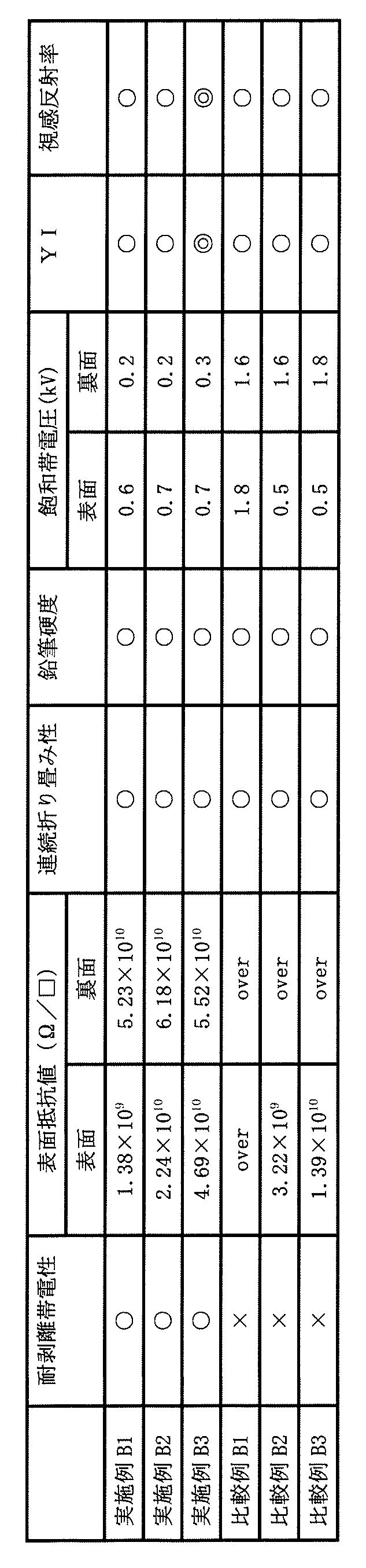
以下、結果について述べる。比較例B1~B3に係る光学フィルムにおいては、第1の帯電防止層および/または第2の帯電防止層が設けられていなかったので、保護フィルムを剥離したときの剥離帯電防止性に劣っていた。これに対し、実施例B1~B3に係る光学フィルムにおいては、第1の帯電防止層および第2の帯電防止層が設けられたので、保護フィルムを剥離したときの剥離帯電防止性に優れていた。 The following describes the results. In the optical films according to Comparative Examples B1 to B3, since the first antistatic layer and / or the second antistatic layer was not provided, the antistatic properties when peeled off the protective film were poor. . In contrast, in the optical films according to Examples B1 to B3, since the first antistatic layer and the second antistatic layer were provided, the antistatic properties when peeled off the protective film were excellent. .
また、実施例B1~B3に係る光学フィルムにおいて、30mm×100mmの長方形にカットして作製したサンプルの短辺(30mm)側を、サンプルの対向する辺部の間隔が3mmとなるように平行に配置された固定部にそれぞれ固定し、光学フィルムを折り畳んだ状態で、70℃で240時間静置する折り畳み静置試験を行った。そして、折り畳み静置試験後に片方の辺部から固定部を外すことによって、折り畳み状態を開放して、室温で30分後に光学フィルムが自然に開く角度である開き角を測定したところ、実施例B2に係る光学フィルムの開き角は100°以上であり、実施例B1、B3に係る光学フィルムの開き角よりも大きかった。なお、開き角としては、第1の帯電防止層が内側となるように折り畳む場合と、第1の帯電防止層が外側となるように折り畳む場合との両方で折り畳み静置試験をし、角度が小さい方を採用した。 In addition, in the optical films according to Examples B1 to B3, the short side (30 mm) side of the sample manufactured by cutting into a rectangle of 30 mm × 100 mm is parallel so that the interval between the opposing side portions of the sample is 3 mm. A folding stationary test was performed in which the optical film was folded and fixed at 70 ° C. for 240 hours while being fixed to the respective fixed portions. And after releasing a fixed part from one side part after a folding stationary test, when a folding state was open | released and the opening angle which is an angle which an optical film opens naturally after 30 minutes at room temperature was measured, Example B2 The opening angle of the optical film according to the present invention was 100 ° or more, which was larger than the opening angle of the optical film according to Examples B1 and B3. In addition, as the opening angle, the folding static test was performed both when the first antistatic layer was folded so that it was on the inside and when the first antistatic layer was folded so that the angle was The smaller one was adopted.
また、実施例B1、B2に係る光学フィルムの第1の帯電防止層および第3に係る光学フィルムのハードコート層のマルテンス硬度を、実施例Aと同様の条件で、測定したところ、第1の帯電防止層およびハードコート層のマルテンス硬度は612MPaであった。 Moreover, when the Martens hardness of the 1st antistatic layer of the optical film which concerns on Example B1, B2 and the hard-coat layer of the optical film which concerns on 3rd was measured on the conditions similar to Example A, it was 1st The Martens hardness of the antistatic layer and the hard coat layer was 612 MPa.
10、30、40、50、60、90、100…光学フィルム
10A、12A、30A、40A、50A、60A、90A、92A、100A、104A…表面
11…樹脂基材
11A…第1の面
11B…第2の面
12…機能層
13…第1の光学調整層
14…第2の光学調整層
15…第3の光学調整層
80、110…画像表示装置
83…表示素子
92、103…第1の帯電防止層
93、105…第2の帯電防止層
102…ハードコート層
104…光学調整層
10, 30, 40, 50, 60, 90, 100 ...
Claims (21)
ポリイミド系樹脂、ポリアミドイミド系樹脂、ポリアミド系樹脂、およびポリエステル系樹脂からなる群から選択される1種以上の樹脂からなる樹脂基材と、
前記樹脂基材の第1の面側に設けられた機能層と、
前記樹脂基材と前記機能層の間に設けられ、かつ前記機能層に隣接した第1の光学調整層と、
を備える、光学フィルム。 A foldable optical film used in an image display device,
A resin base material composed of one or more resins selected from the group consisting of a polyimide resin, a polyamideimide resin, a polyamide resin, and a polyester resin;
A functional layer provided on the first surface side of the resin substrate;
A first optical adjustment layer provided between the resin substrate and the functional layer and adjacent to the functional layer;
An optical film comprising:
光透過性基材と、
前記光透過性基材の第1の面側に設けられた第1の帯電防止層と、
前記光透過性基材の前記第1の面とは反対側の第2の面側に設けられた第2の帯電防止層と、
を備える、光学フィルム。 A foldable optical film used in an image display device,
A light transmissive substrate;
A first antistatic layer provided on the first surface side of the light transmissive substrate;
A second antistatic layer provided on a second surface side opposite to the first surface of the light transmissive substrate;
An optical film comprising:
前記表示素子よりも観察者側に配置された請求項1または12に記載の光学フィルムと、
を備えることを特徴とする、折り畳み可能な画像表示装置。 A display element;
The optical film according to claim 1 or 12, which is disposed closer to the viewer than the display element;
A foldable image display device comprising:
Applications Claiming Priority (4)
| Application Number | Priority Date | Filing Date | Title |
|---|---|---|---|
| JP2017-064583 | 2017-03-29 | ||
| JP2017064583 | 2017-03-29 | ||
| JP2018-035426 | 2018-02-28 | ||
| JP2018035426A JP7119424B2 (en) | 2017-03-02 | 2018-02-28 | Optical film and image display device |
Publications (1)
| Publication Number | Publication Date |
|---|---|
| WO2018180304A1 true WO2018180304A1 (en) | 2018-10-04 |
Family
ID=63675360
Family Applications (1)
| Application Number | Title | Priority Date | Filing Date |
|---|---|---|---|
| PCT/JP2018/008733 Ceased WO2018180304A1 (en) | 2017-03-29 | 2018-03-07 | Optical film and image display device |
Country Status (1)
| Country | Link |
|---|---|
| WO (1) | WO2018180304A1 (en) |
Cited By (6)
| Publication number | Priority date | Publication date | Assignee | Title |
|---|---|---|---|---|
| JPWO2021060560A1 (en) * | 2019-09-27 | 2021-04-01 | ||
| CN113270557A (en) * | 2020-02-14 | 2021-08-17 | 三星显示有限公司 | Electronic device |
| JPWO2021182453A1 (en) * | 2020-03-09 | 2021-09-16 | ||
| JPWO2021182443A1 (en) * | 2020-03-09 | 2021-09-16 | ||
| JPWO2022239821A1 (en) * | 2021-05-13 | 2022-11-17 | ||
| EP4169974A4 (en) * | 2020-06-23 | 2024-07-17 | Kolon Industries, Inc. | Multi-structured film having improved interference fringe, and display device comprising same |
Citations (10)
| Publication number | Priority date | Publication date | Assignee | Title |
|---|---|---|---|---|
| JP2008242425A (en) * | 2007-02-26 | 2008-10-09 | Seiko Epson Corp | Optical article and manufacturing method thereof |
| JP2009263567A (en) * | 2008-04-28 | 2009-11-12 | Sumitomo Osaka Cement Co Ltd | Coating material for forming antistatic hard coat film, antistatic hard coat film, plastic base material with antistatic hard coat film, and method for manufacturing plastic base material with antistatic hard coat film |
| JP2010113175A (en) * | 2008-11-07 | 2010-05-20 | Ube Nitto Kasei Co Ltd | Laminate |
| WO2011013798A1 (en) * | 2009-07-31 | 2011-02-03 | 名阪真空工業株式会社 | Display film and manufacturing method therefor |
| JP2014040037A (en) * | 2012-08-22 | 2014-03-06 | Toray Advanced Film Co Ltd | Hard coat film, transparent conductive film, and touch panel |
| JP2014046608A (en) * | 2012-08-31 | 2014-03-17 | Dainippon Printing Co Ltd | Laminate, polarizing plate, liquid crystal panel, touch panel sensor, touch panel device, and picture display device |
| WO2017014198A1 (en) * | 2015-07-17 | 2017-01-26 | 大日本印刷株式会社 | Laminate for optical members and image display device |
| JP6216907B1 (en) * | 2016-08-23 | 2017-10-18 | リンテック株式会社 | Hard coat film |
| WO2017200042A1 (en) * | 2016-05-20 | 2017-11-23 | 大日本印刷株式会社 | Optical laminated body, and image display device |
| JP2017207754A (en) * | 2016-05-19 | 2017-11-24 | 東友ファインケム株式会社Dongwoo Fine−Chem Co., Ltd. | Hard coating film and flexible display having the same |
-
2018
- 2018-03-07 WO PCT/JP2018/008733 patent/WO2018180304A1/en not_active Ceased
Patent Citations (10)
| Publication number | Priority date | Publication date | Assignee | Title |
|---|---|---|---|---|
| JP2008242425A (en) * | 2007-02-26 | 2008-10-09 | Seiko Epson Corp | Optical article and manufacturing method thereof |
| JP2009263567A (en) * | 2008-04-28 | 2009-11-12 | Sumitomo Osaka Cement Co Ltd | Coating material for forming antistatic hard coat film, antistatic hard coat film, plastic base material with antistatic hard coat film, and method for manufacturing plastic base material with antistatic hard coat film |
| JP2010113175A (en) * | 2008-11-07 | 2010-05-20 | Ube Nitto Kasei Co Ltd | Laminate |
| WO2011013798A1 (en) * | 2009-07-31 | 2011-02-03 | 名阪真空工業株式会社 | Display film and manufacturing method therefor |
| JP2014040037A (en) * | 2012-08-22 | 2014-03-06 | Toray Advanced Film Co Ltd | Hard coat film, transparent conductive film, and touch panel |
| JP2014046608A (en) * | 2012-08-31 | 2014-03-17 | Dainippon Printing Co Ltd | Laminate, polarizing plate, liquid crystal panel, touch panel sensor, touch panel device, and picture display device |
| WO2017014198A1 (en) * | 2015-07-17 | 2017-01-26 | 大日本印刷株式会社 | Laminate for optical members and image display device |
| JP2017207754A (en) * | 2016-05-19 | 2017-11-24 | 東友ファインケム株式会社Dongwoo Fine−Chem Co., Ltd. | Hard coating film and flexible display having the same |
| WO2017200042A1 (en) * | 2016-05-20 | 2017-11-23 | 大日本印刷株式会社 | Optical laminated body, and image display device |
| JP6216907B1 (en) * | 2016-08-23 | 2017-10-18 | リンテック株式会社 | Hard coat film |
Cited By (21)
| Publication number | Priority date | Publication date | Assignee | Title |
|---|---|---|---|---|
| JP2025081324A (en) * | 2019-09-27 | 2025-05-27 | 大日本印刷株式会社 | Resin layer, optical film and image display device |
| JP7626069B2 (en) | 2019-09-27 | 2025-02-04 | 大日本印刷株式会社 | Resin layer, optical film and image display device |
| JPWO2021060560A1 (en) * | 2019-09-27 | 2021-04-01 | ||
| US12219696B2 (en) * | 2020-02-14 | 2025-02-04 | Samsung Display Co., Ltd. | Electronic device |
| CN113270557A (en) * | 2020-02-14 | 2021-08-17 | 三星显示有限公司 | Electronic device |
| US20210259093A1 (en) * | 2020-02-14 | 2021-08-19 | Samsung Display Co., Ltd. | Electronic device |
| JPWO2021182443A1 (en) * | 2020-03-09 | 2021-09-16 | ||
| CN115461213B (en) * | 2020-03-09 | 2024-08-02 | 大日本印刷株式会社 | Laminate for flexible display device, laminate for display device, and flexible display device |
| US12602080B2 (en) | 2020-03-09 | 2026-04-14 | Dai Nippon Printing Co., Ltd. | Stacked body for flexible display device, stacked body for display device and flexible display device |
| CN115461214A (en) * | 2020-03-09 | 2022-12-09 | 大日本印刷株式会社 | Laminate for flexible display device, laminate for display device, and flexible display device |
| CN115461213A (en) * | 2020-03-09 | 2022-12-09 | 大日本印刷株式会社 | Laminate for flexible display device, laminate for display device, and flexible display device |
| JP7757953B2 (en) | 2020-03-09 | 2025-10-22 | 大日本印刷株式会社 | Laminate for flexible display device, laminate for display device, and flexible display device |
| TWI889773B (en) * | 2020-03-09 | 2025-07-11 | 日商大日本印刷股份有限公司 | Stacked body for flexible display, stacked body for display and flexible display |
| JPWO2021182453A1 (en) * | 2020-03-09 | 2021-09-16 | ||
| CN115461214B (en) * | 2020-03-09 | 2024-08-06 | 大日本印刷株式会社 | Laminate for flexible display device, laminate for display device, and flexible display device |
| WO2021182443A1 (en) * | 2020-03-09 | 2021-09-16 | 大日本印刷株式会社 | Laminate for flexible display device, laminate for display device, and flexible display device |
| WO2021182453A1 (en) * | 2020-03-09 | 2021-09-16 | 大日本印刷株式会社 | Laminate for flexible display device, laminate for display device, and flexible display device |
| EP4169974A4 (en) * | 2020-06-23 | 2024-07-17 | Kolon Industries, Inc. | Multi-structured film having improved interference fringe, and display device comprising same |
| JPWO2022239821A1 (en) * | 2021-05-13 | 2022-11-17 | ||
| CN117279781A (en) * | 2021-05-13 | 2023-12-22 | 大日本印刷株式会社 | Laminate for display device and display device |
| WO2022239821A1 (en) * | 2021-05-13 | 2022-11-17 | 大日本印刷株式会社 | Multilayer body for display devices, and display device |
Similar Documents
| Publication | Publication Date | Title |
|---|---|---|
| JP7119424B2 (en) | Optical film and image display device | |
| JP7831471B2 (en) | Optical films and image display devices | |
| JP7331829B2 (en) | Optical film and image display device | |
| JP7667635B2 (en) | Optical film and image display device | |
| JP6773118B2 (en) | Optical film and image display device | |
| JP7000701B2 (en) | Optical film and image display device | |
| WO2018180304A1 (en) | Optical film and image display device | |
| JP7409456B2 (en) | Optical films and image display devices | |
| JP7572143B2 (en) | Optical film and image display device | |
| JPWO2018070523A1 (en) | Optical film and image display device | |
| JP2019045804A (en) | Polyimide film, optical film, and image display device | |
| JP7435640B2 (en) | Light transparent film with protective film and protective film | |
| JP2025081324A (en) | Resin layer, optical film and image display device | |
| TWI731228B (en) | Optical film and image display device | |
| WO2020179643A1 (en) | Resin layer, optical film, and image display device | |
| US20250258328A1 (en) | Optical film and image display device |
Legal Events
| Date | Code | Title | Description |
|---|---|---|---|
| 121 | Ep: the epo has been informed by wipo that ep was designated in this application |
Ref document number: 18775944 Country of ref document: EP Kind code of ref document: A1 |
|
| NENP | Non-entry into the national phase |
Ref country code: DE |
|
| 122 | Ep: pct application non-entry in european phase |
Ref document number: 18775944 Country of ref document: EP Kind code of ref document: A1 |