JPWO2020175475A1 - プリント配線板 - Google Patents
プリント配線板 Download PDFInfo
- Publication number
- JPWO2020175475A1 JPWO2020175475A1 JP2021502272A JP2021502272A JPWO2020175475A1 JP WO2020175475 A1 JPWO2020175475 A1 JP WO2020175475A1 JP 2021502272 A JP2021502272 A JP 2021502272A JP 2021502272 A JP2021502272 A JP 2021502272A JP WO2020175475 A1 JPWO2020175475 A1 JP WO2020175475A1
- Authority
- JP
- Japan
- Prior art keywords
- pattern
- conductive pattern
- base film
- wiring board
- printed wiring
- Prior art date
- Legal status (The legal status is an assumption and is not a legal conclusion. Google has not performed a legal analysis and makes no representation as to the accuracy of the status listed.)
- Pending
Links
Images


Classifications
-
- H—ELECTRICITY
- H05—ELECTRIC TECHNIQUES NOT OTHERWISE PROVIDED FOR
- H05K—PRINTED CIRCUITS; CASINGS OR CONSTRUCTIONAL DETAILS OF ELECTRIC APPARATUS; MANUFACTURE OF ASSEMBLAGES OF ELECTRICAL COMPONENTS
- H05K1/00—Printed circuits
- H05K1/02—Details
-
- H—ELECTRICITY
- H10—SEMICONDUCTOR DEVICES; ELECTRIC SOLID-STATE DEVICES NOT OTHERWISE PROVIDED FOR
- H10W—GENERIC PACKAGES, INTERCONNECTIONS, CONNECTORS OR OTHER CONSTRUCTIONAL DETAILS OF DEVICES COVERED BY CLASS H10
- H10W70/00—Package substrates; Interposers; Redistribution layers [RDL]
- H10W70/60—Insulating or insulated package substrates; Interposers; Redistribution layers
Landscapes
- Engineering & Computer Science (AREA)
- Microelectronics & Electronic Packaging (AREA)
- Manufacturing Of Printed Wiring (AREA)
- Structure Of Printed Boards (AREA)
Applications Claiming Priority (3)
| Application Number | Priority Date | Filing Date | Title |
|---|---|---|---|
| JP2019034030 | 2019-02-27 | ||
| JP2019034030 | 2019-02-27 | ||
| PCT/JP2020/007485 WO2020175475A1 (fr) | 2019-02-27 | 2020-02-25 | Carte de circuit imprimé |
Publications (1)
| Publication Number | Publication Date |
|---|---|
| JPWO2020175475A1 true JPWO2020175475A1 (ja) | 2021-12-23 |
Family
ID=72239199
Family Applications (1)
| Application Number | Title | Priority Date | Filing Date |
|---|---|---|---|
| JP2021502272A Pending JPWO2020175475A1 (ja) | 2019-02-27 | 2020-02-25 | プリント配線板 |
Country Status (3)
| Country | Link |
|---|---|
| JP (1) | JPWO2020175475A1 (fr) |
| CN (1) | CN113383412A (fr) |
| WO (1) | WO2020175475A1 (fr) |
Family Cites Families (6)
| Publication number | Priority date | Publication date | Assignee | Title |
|---|---|---|---|---|
| JP3241468B2 (ja) * | 1992-12-28 | 2001-12-25 | ソニー株式会社 | Fpcにおけるコネクター用端子部の製造方法 |
| JP3864093B2 (ja) * | 2002-01-10 | 2006-12-27 | シャープ株式会社 | プリント配線基板、電波受信用コンバータおよびアンテナ装置 |
| JP4407471B2 (ja) * | 2004-10-29 | 2010-02-03 | パナソニック株式会社 | フレキシブル配線基板とそれを用いた電子機器およびその製造方法 |
| JP4969257B2 (ja) * | 2007-01-29 | 2012-07-04 | 京セラ株式会社 | 配線基板およびそれを用いた半導体素子の実装構造体 |
| JP2011249711A (ja) * | 2010-05-31 | 2011-12-08 | Kyocera Corp | 配線基板およびその実装構造体 |
| WO2018159023A1 (fr) * | 2017-03-01 | 2018-09-07 | 住友電気工業株式会社 | Carte de circuit imprimé souple, procédé de fabrication de connecteur et connecteur |
-
2020
- 2020-02-25 CN CN202080011580.8A patent/CN113383412A/zh active Pending
- 2020-02-25 JP JP2021502272A patent/JPWO2020175475A1/ja active Pending
- 2020-02-25 WO PCT/JP2020/007485 patent/WO2020175475A1/fr not_active Ceased
Also Published As
| Publication number | Publication date |
|---|---|
| WO2020175475A1 (fr) | 2020-09-03 |
| CN113383412A (zh) | 2021-09-10 |
Similar Documents
| Publication | Publication Date | Title |
|---|---|---|
| US9155209B2 (en) | Flex-rigid printed wiring board and manufacturing method thereof | |
| TWI411367B (zh) | 軟性線路基板的製造方法 | |
| US11690178B2 (en) | Multilayer printed wiring board and method of manufacturing the same | |
| CN100454502C (zh) | 多层布线基板的制造方法和多层布线基板及使用其的电子装置 | |
| JP7161620B2 (ja) | キャリア付金属箔及びその製造方法 | |
| JP6826197B2 (ja) | プリント配線板及びその製造方法 | |
| JP5379281B2 (ja) | プリント基板の製造方法 | |
| CN107920415A (zh) | 具厚铜线路的电路板及其制作方法 | |
| CN102159035A (zh) | 印刷电路板及其制作方法和制作双面印刷电路板的方法 | |
| JP2005317836A (ja) | 配線回路基板およびその製造方法 | |
| JP4799902B2 (ja) | 配線回路基板および配線回路基板の製造方法 | |
| CN109673111B (zh) | 电路板的制作方法 | |
| CN108024442B (zh) | 布线电路基板及其制造方法 | |
| JP7464040B2 (ja) | プリント配線板及びプリント配線板の製造方法 | |
| JP6013750B2 (ja) | プリント配線板およびその製造方法 | |
| JP2001111201A (ja) | 配線板の製造方法およびそれを用いて製造された配線板 | |
| JP2011003246A (ja) | サスペンション用基板 | |
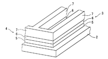
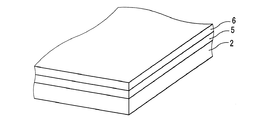
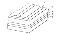
| JPWO2020175475A1 (ja) | プリント配線板 | |
| CN104768324A (zh) | 核心基材与线路板的制作方法 | |
| CN106332444B (zh) | 电路板及其制作方法 | |
| US20150027761A1 (en) | Printed circuit board and method of manufacturing the same | |
| JP2007317900A (ja) | 配線回路基板およびその製造方法 | |
| US12232261B2 (en) | Printed wiring board | |
| JP2007184441A (ja) | 配線基板の製造方法 | |
| KR100736146B1 (ko) | 플렉서블 회로기판의 제조방법 |
Legal Events
| Date | Code | Title | Description |
|---|---|---|---|
| RD02 | Notification of acceptance of power of attorney |
Free format text: JAPANESE INTERMEDIATE CODE: A7422 Effective date: 20220601 |