KR100246162B1 - How to Form a Transistor in a Peripheral Circuit - Google Patents
How to Form a Transistor in a Peripheral Circuit Download PDFInfo
- Publication number
- KR100246162B1 KR100246162B1 KR1019970704922A KR19970704922A KR100246162B1 KR 100246162 B1 KR100246162 B1 KR 100246162B1 KR 1019970704922 A KR1019970704922 A KR 1019970704922A KR 19970704922 A KR19970704922 A KR 19970704922A KR 100246162 B1 KR100246162 B1 KR 100246162B1
- Authority
- KR
- South Korea
- Prior art keywords
- polysilicon layer
- peripheral
- etching
- patterning
- memory cell
- Prior art date
- Legal status (The legal status is an assumption and is not a legal conclusion. Google has not performed a legal analysis and makes no representation as to the accuracy of the status listed.)
- Expired - Fee Related
Links
Images


Classifications
-
- H—ELECTRICITY
- H10—SEMICONDUCTOR DEVICES; ELECTRIC SOLID-STATE DEVICES NOT OTHERWISE PROVIDED FOR
- H10B—ELECTRONIC MEMORY DEVICES
- H10B12/00—Dynamic random access memory [DRAM] devices
- H10B12/01—Manufacture or treatment
-
- H—ELECTRICITY
- H10—SEMICONDUCTOR DEVICES; ELECTRIC SOLID-STATE DEVICES NOT OTHERWISE PROVIDED FOR
- H10B—ELECTRONIC MEMORY DEVICES
- H10B10/00—Static random access memory [SRAM] devices
- H10B10/12—Static random access memory [SRAM] devices comprising a MOSFET load element
-
- H—ELECTRICITY
- H10—SEMICONDUCTOR DEVICES; ELECTRIC SOLID-STATE DEVICES NOT OTHERWISE PROVIDED FOR
- H10B—ELECTRONIC MEMORY DEVICES
- H10B10/00—Static random access memory [SRAM] devices
- H10B10/18—Peripheral circuit regions
-
- H—ELECTRICITY
- H10—SEMICONDUCTOR DEVICES; ELECTRIC SOLID-STATE DEVICES NOT OTHERWISE PROVIDED FOR
- H10B—ELECTRONIC MEMORY DEVICES
- H10B12/00—Dynamic random access memory [DRAM] devices
- H10B12/01—Manufacture or treatment
- H10B12/02—Manufacture or treatment for one transistor one-capacitor [1T-1C] memory cells
- H10B12/05—Making the transistor
-
- H—ELECTRICITY
- H10—SEMICONDUCTOR DEVICES; ELECTRIC SOLID-STATE DEVICES NOT OTHERWISE PROVIDED FOR
- H10B—ELECTRONIC MEMORY DEVICES
- H10B12/00—Dynamic random access memory [DRAM] devices
- H10B12/01—Manufacture or treatment
- H10B12/09—Manufacture or treatment with simultaneous manufacture of the peripheral circuit region and memory cells
-
- Y—GENERAL TAGGING OF NEW TECHNOLOGICAL DEVELOPMENTS; GENERAL TAGGING OF CROSS-SECTIONAL TECHNOLOGIES SPANNING OVER SEVERAL SECTIONS OF THE IPC; TECHNICAL SUBJECTS COVERED BY FORMER USPC CROSS-REFERENCE ART COLLECTIONS [XRACs] AND DIGESTS
- Y10—TECHNICAL SUBJECTS COVERED BY FORMER USPC
- Y10S—TECHNICAL SUBJECTS COVERED BY FORMER USPC CROSS-REFERENCE ART COLLECTIONS [XRACs] AND DIGESTS
- Y10S257/00—Active solid-state devices, e.g. transistors, solid-state diodes
- Y10S257/903—FET configuration adapted for use as static memory cell
- Y10S257/904—FET configuration adapted for use as static memory cell with passive components,, e.g. polysilicon resistors
Landscapes
- Engineering & Computer Science (AREA)
- Manufacturing & Machinery (AREA)
- Semiconductor Memories (AREA)
Abstract
본 발명은 다이내믹 랜덤 액세스 메모리 장치(DRAM) 또는 스태틱 랜덤 액세스 메모리 장치(SRAM)의 주변 회로 내 트랜지스터를 형성하는 방법에 관한 것이다. 본 발명에 따르면, 메모리 셀 어레이 내의 트랜지스터 게이트, 커패시터 전극 또는 다른 소자들은 주변 트랜지스터 게이트의 형성과 동시에 형성된다.The present invention relates to a method of forming a transistor in a peripheral circuit of a dynamic random access memory device (DRAM) or a static random access memory device (SRAM). In accordance with the present invention, transistor gates, capacitor electrodes or other elements in the memory cell array are formed simultaneously with the formation of the peripheral transistor gates.
Description
일반적으로, 집적 회로는 단일 반도체 웨이퍼 상에 다수의 동일한 회로 패턴을 형성함으로써 대량 생산된다. 대개 반도체 장치로서 일컬어지는 집적 회로는 전도체, 부도체 또는 반도체로 구성된 각종 물질로 제조된다. 제조 비용을 감소시키고 품질 및 신뢰성을 향상시키기 위하여는 제조 공정 단계를 감소시켜 결함 발생 확률을 감소시키는 것이 유리하다. 이러한 방법을 통해, 전자 장비는 신뢰성이 향상되고 조립 및 패키지 비용이 최소화되며 회로 성능이 향상된다.In general, integrated circuits are mass produced by forming multiple identical circuit patterns on a single semiconductor wafer. Integrated circuits, often referred to as semiconductor devices, are made of various materials consisting of conductors, nonconductors, or semiconductors. In order to reduce manufacturing costs and improve quality and reliability, it is advantageous to reduce manufacturing process steps to reduce the probability of defect occurrence. In this way, electronic equipment is more reliable, assembly and packaging costs are minimized, and circuit performance is improved.
DRAM 및 SRAM과 같은 랜덤 액세스 메모리 장치는 데이타를 저장하기 위한 메모리 셀들과, 메모리셀들 내외의 신호들을 스위칭하기 위한 주변 회로들을 포함한다. 전체 장치의 제조에 필요한 공정 단계의 수를 감소시키기 위하여는 메모리 셀 어레이 내에 트랜지스터, 커패시터 및 다른 소자들을 형성함과 동시에 주변 회로 내의 트랜지스터들을 형성하는 것이 바람직하다. 메모리 셀의 형성시, 메모리 셀 소자들을 형성하기 위하여 폴리실리콘 및 산화물 절연체로 된 층들이 침적되고 패터닝되고 에칭된다. 동시에, 이들 폴리실리콘 및 산화물 층들은 주변 회로 트랜지스터들이 형성되는 칩 영역에도 침적되며 어느 정도로는 더 처리된다. 전체 공정 흐름의 효율은 주변 회로 내 트랜지스터의 형성이 메모리 셀 소자들의 형성과 통합될 수 있을 정도로 향상되었다.Random access memory devices, such as DRAM and SRAM, include memory cells for storing data and peripheral circuits for switching signals in and out of the memory cells. In order to reduce the number of process steps required for the manufacture of the overall device, it is desirable to form transistors in peripheral circuits while simultaneously forming transistors, capacitors and other elements in the memory cell array. In forming the memory cell, layers of polysilicon and oxide insulators are deposited, patterned and etched to form memory cell elements. At the same time, these polysilicon and oxide layers are also deposited to the chip region where peripheral circuit transistors are formed and to some extent processed. The efficiency of the overall process flow has been improved so that the formation of transistors in the peripheral circuit can be integrated with the formation of memory cell elements.
<발명의 요약>Summary of the Invention
본 발명의 일반적인 목적 및 주 목적은 반도체 메모리 장치의 메모리 셀 어레이 내의 저항, 커패시터 및 다른 소자들의 형성과 주변 회로 내의 트랜지스터의 형성을 통합한 방법을 제공하는 데 있다.It is a general and main object of the present invention to provide a method that integrates the formation of resistors, capacitors and other elements in a memory cell array of a semiconductor memory device with the formation of transistors in peripheral circuits.
상기한 목적 및 다른 목적들을 달성하기 위하여, 기판 상의 메모리 셀 어레이 영역 및 주변 영역에 게이트 산화층, 및 상기 게이트 산화층 상부에 적어도 하나의 폴리실리콘층을 형성하는 단계, 및 상기 폴리실리콘층(들)을 패터닝하고 에칭하여 어레이 영역 내의 저항, 커패시터 전극 또는 다른 소자들 및 주변 영역 내의 주변 트랜지스터 게이트를 동시에 형성하는 단계를 포함하는 랜덤 액세스 메모리 장치의 주변 영역에 트랜지스터를 형성하는 방법이 개발되었다.In order to achieve the above and other objects, forming a gate oxide layer in the memory cell array region and the peripheral region on the substrate, and at least one polysilicon layer on the gate oxide layer, and the polysilicon layer (s) A method has been developed for forming a transistor in a peripheral region of a random access memory device comprising patterning and etching to simultaneously form a resistor, capacitor electrode or other elements in the array region, and a peripheral transistor gate in the peripheral region.
본 발명의 한 특징에 따르면, 주변 트랜지스터 게이트는 스태틱 랜덤 액세스 메모리(SRAM)의 메모리 셀 어레이 내의 부하 저항의 형성과 동시에 형성된다. 이러한 본 발명의 특징에 따라, 주변 영역 내의 폴리실리콘층을 패터닝하고 에칭하는 단계는 부하 저항의 형성이 완료되는, 메모리 셀 어레이 영역 내의 폴리실리콘층의 패터닝 및 에칭 단계와 동시에, 그리고 그 일부로서 실시된다. 또한, 주변 게이트는 SRAM 메모리 셀 어레이 영역 내의 접지 라인 및 비트 라인 콘택 랜딩(landing) 패드의 형성과 동시에 형성될 수 있다. 즉, 주변 영역 내의 폴리실리콘층의 패터닝 및 에칭 단계는 접지 라인 및 비트 라인 콘택 랜딩 패드가 형성되는, 메모리 셀 어레이 영역 내의 폴리실리콘층의 패터닝 및 에칭과 동시에, 그리고 그 일부로서 실시된다.According to one aspect of the invention, the peripheral transistor gate is formed simultaneously with the formation of a load resistor in the memory cell array of the static random access memory (SRAM). In accordance with this aspect of the invention, patterning and etching the polysilicon layer in the peripheral region is performed simultaneously with, and as part of, the patterning and etching of the polysilicon layer in the memory cell array region, where formation of a load resistor is completed. do. In addition, the peripheral gate may be formed simultaneously with the formation of the ground line and bit line contact landing pads in the SRAM memory cell array region. That is, the patterning and etching of the polysilicon layer in the peripheral region is performed simultaneously with and as part of the patterning and etching of the polysilicon layer in the memory cell array region in which the ground line and bit line contact landing pads are formed.
본 발명의 다른 특징에 따르면, 주변 트랜지스터 게이트는 다이내믹 랜덤 액세스 메모리(DRAM)의 메모리 셀 어레이 영역 내의 커패시터 전극의 형성과 동시에 형성된다. 이러한 본 발명의 특징에 따라, 주변 영역 내의 폴리실리콘층의 패터닝 및 에칭 단계는 커패시터 전극이 형성되는, 메모리 셀 어레이 영역 내의 폴리실리콘층의 패터닝 및 에칭 단계와 동시에, 그리고 그 일부로서 실시된다.According to another feature of the invention, the peripheral transistor gate is formed simultaneously with the formation of the capacitor electrode in the memory cell array region of the dynamic random access memory (DRAM). In accordance with this aspect of the invention, the patterning and etching steps of the polysilicon layer in the peripheral region are performed simultaneously with and as part of the patterning and etching steps of the polysilicon layer in the memory cell array region where the capacitor electrodes are formed.
본 발명의 전술한 목적 및 다른 목적들, 장점들 및 신규한 특징들은 본 발명을 구현하는 최상 방식을 설명함으로써 본 발명의 바람직한 실시예들만을 도시하고 설명한 아래의 상세한 설명으로부터 당해 분야의 기술자들에게 명백해질 것이다. 본 발명의 영역 및 사상을 벗어나지 않고도 본 발명은 여러 상이한 실시예들이 가능하고 다른 응용 분야에서 사용될 수 있으며, 이에 대한 몇몇 세부 사항들은 여러 자명한 측면에서의 변형이 가능하다. 따라서, 도면들 및 설명들은 본질상 제한적인 것이 아니라 예시적인 것으로 고려되어야 한다.The foregoing and other objects, advantages and novel features of the present invention will be described to those skilled in the art from the following detailed description showing only the preferred embodiments of the present invention by describing the best way of implementing the present invention. Will be obvious. The invention is capable of many different embodiments and can be used in other applications, without departing from the scope and spirit of the invention, some details of which are capable of modification in various obvious respects. Accordingly, the drawings and descriptions are to be regarded as illustrative in nature and not as restrictive.
본 발명은 반도체 메모리 장치의 제조에 관한 것으로서, 특히 랜덤 액세스 메모리 장치의 주변 회로 내의 트랜지스터 형성 방법에 관한 것이다.BACKGROUND OF THE INVENTION 1. Field of the Invention The present invention relates to the manufacture of semiconductor memory devices, and more particularly to a method of forming transistors in peripheral circuits of random access memory devices.
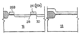
도 1은 반도체 메모리 장치의 메모리 셀 어레이 영역 및 주변 영역을 나타내는 개략적인 평면도.1 is a schematic plan view showing a memory cell array region and a peripheral region of a semiconductor memory device;
도 2는 본 발명에 따라 구성된 스태틱 랜덤 액세스 메모리(SRAM)의 일부를 나타내는 단면도.2 is a cross-sectional view of a portion of a static random access memory (SRAM) constructed in accordance with the present invention.
도 3A-3F는 본 발명의 바람직한 실시예를 나타내는 여러 형성 단계에서의 도 2의 SRAM의 단면도들.3A-3F are cross-sectional views of the SRAM of FIG. 2 at various stages of formation showing a preferred embodiment of the present invention.
도 4A-4F는 본 발명의 다른 실시예를 나타내는 여러 형성 단계에서의 SRAM의 단면도들.4A-4F are cross-sectional views of an SRAM at various stages of formation, showing another embodiment of the invention.
도 5는 본 발명에 따라 구성된 다이내믹 랜덤 액세스 메모리(DRAM)의 일부를 나타내는 단면도.5 is a cross-sectional view showing a portion of a dynamic random access memory (DRAM) constructed in accordance with the present invention.
도 6A-6F는 본 발명의 다른 실시예를 나타내는 여러 형성 단계에서의 도 4의 DRAM의 단면도들.6A-6F are cross-sectional views of the DRAM of FIG. 4 at various forming stages representing another embodiment of the present invention.
도면들은 그에 도시된 반도체 메모리 장치의 부분들의 실제 도면이 아니라 본 발명을 설명하기 위해 사용되는 개략적인 도면들이다.The drawings are schematic drawings used to explain the invention rather than the actual drawings of portions of the semiconductor memory device shown therein.
현재, 상보형 금속-산화물-반도체(CMOS) 기술이 가장 보편적으로 사용되는 집적 회로 기술이다. 일반적으로, CMOS는 n 채널 및 p 채널 MOS 전계 효과 트랜지스터(MOSFET)들이 보완적인 방식으로 사용되는 집적 회로를 나타낸다. 본 발명은 주변 p 채널 트랜지스터의 형성과 관련하여 설명될 것이다. 현재, p 채널 및 n 채널 주변 트랜지스터 게이트들은 어레이 내의 n 채널 트랜지스터 게이트의 형성시에 형성된다. 결과적으로, 주변 영역 내의 p 채널 트랜지스터 게이트들에 인접한 기판 콘택 영역들은 n형 도펀트들이 주입되는 것을 방지하기 위하여 n 채널 소스/드레인 영역의 형성시 마스킹되어야 한다. 본 발명은 n 채널 소스/드레인 영역의 형성 후에 주변 p 채널 트랜지스터 게이트들이 형성되도록 하여 상기 마스킹 단계를 제거할 수 있게 한다. 그러나, 본 발명은 다른 집적 회로 공정들 및 구조들에도 사용될 수 있다.Currently, complementary metal-oxide-semiconductor (CMOS) technology is the most commonly used integrated circuit technology. In general, CMOS represents an integrated circuit in which n-channel and p-channel MOS field effect transistors (MOSFETs) are used in a complementary manner. The invention will be described with reference to the formation of peripheral p-channel transistors. Currently, p-channel and n-channel peripheral transistor gates are formed in the formation of n-channel transistor gates in an array. As a result, substrate contact regions adjacent to the p-channel transistor gates in the peripheral region should be masked in the formation of the n-channel source / drain region to prevent the n-type dopants from being implanted. The present invention allows peripheral p-channel transistor gates to be formed after the formation of the n-channel source / drain region to eliminate the masking step. However, the present invention may be used for other integrated circuit processes and structures.
집적 회로의 형성은 포토리소그래픽 마스킹 및 에칭 단계들을 포함한다. 이러한 공정은 형성될 소자의 패턴을 구비한 포토리소그래픽 마스크를 생성하는 공정, 포토레지스트라는 감광 물질을 웨이퍼에 코팅하는 공정, 웨이퍼에 코팅된 포토레지스트를 마스크를 통해 자외선에 노출시켜 포토레지스트의 일부를 연화 또는 경화(포지티브 또는 네가티브 포토레지스트의 사용 여부에 의존)시키는 공정, 포토레지스트의 연화된 부분들을 제거하는 공정, 포토레지스트에 의해 마스킹되지 않은 물질들을 에칭하여 제거하는 공정, 및 잔류 포토레지스트를 제거하는 공정으로 이루어진다. 이러한 포토리소그래픽 마스킹 및 에칭 공정은 이하 "패터닝 및 에칭 공정"으로 참조된다.Formation of the integrated circuit includes photolithographic masking and etching steps. Such a process includes a process of generating a photolithographic mask having a pattern of a device to be formed, a process of coating a photosensitive material called a photoresist on a wafer, and exposing the photoresist coated on the wafer to ultraviolet rays through a mask to form part of the photoresist Softening or curing (depending on the use of positive or negative photoresist), removing the softened portions of the photoresist, etching to remove unmasked materials by the photoresist, and residual photoresist Removal process. This photolithographic masking and etching process is referred to below as the "patterning and etching process".
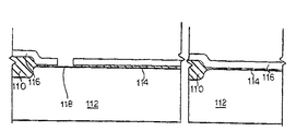
도 1은 메모리 셀 어레이 영역(4) 및 주변 영역(6)을 포함하는 반도체 메모리 장치(2)를 나타내는 개략적인 평면도이다. 메모리 장치(2)는 특히 DRAM들 및 SRAM들을 포함해, 본 발명이 적용될 수 있는 각종 메모리 장치들을 나타낸다. 본 발명에 따라 DRAM 및 SRAM의 주변 회로 내의 p 채널 트랜지스터를 형성하는 방법들이 본 발명의 바람직한 실시예에 따라 형성된 SRAM에 대하여는 도 2 및 3A-3F를, 본 발명의 다른 실시예에 따라 형성된 SRAM에 대하여는 도 4A-4F를, 그리고 DRAM에 대하여는 도 5 및 도 6A-6E를 참조하여 아래에 상세히 설명된다. 이러한 개략적인 단면도들 각각은 도시된 특정 장치의 구조를 형성하기 위하여 실시되는 공정 단계의 수를 나타낸다. 물질 침적, 패터닝 및 에칭, 그리고 이온 주입에 대하여 설명된 기술들은 당해 분야에 공지되어 있다.1 is a schematic plan view of a semiconductor memory device 2 including a memory cell array region 4 and a
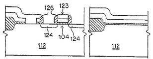
도 2를 참조하면, 트랜지스터(104) 및 부하 저항(106)을 포함한 트랜지스터 SRAM 메모리 셀의 일부가 도 2의 좌측에 도시되어 있으며, 주변 회로 내 하나의 주변 p 채널 트랜지스터(108)가 도 2의 우측에 도시되어 있다. 트랜지스터(104)는 메모리 셀 어레이 내의 액세스 트랜지스터 또는 풀다운 트랜지스터를 나타낸다. 간단히 하기 위하여, 이하 트랜지스터(104)는 액세스 트랜지스터로 참조된다. 이제, 도 2에 도시된 장치를 제조하는 공정이 도 3A-3F를 참조하여 설명된다.Referring to FIG. 2, a portion of a transistor SRAM memory
도 3A를 참조하면, p형 단결정 실리콘 기판(112)이 산화되어 게이트 산화물층(114) 및 두꺼운 필드 산화물 영역(110)이 형성된다. 필드 산화물 영역(110)은 메모리 셀 어레이와 주변부 사이 및 어레이 내 개별 메모리 셀들 간의 전기적 절연을 제공한다. 바람직한 실시예에서는 게이트 산화물층(114) 상부에 화학 기상 침적(CVD) 방식으로 선택 폴리실리콘층(116)이 형성된다. 폴리실리콘층(116)은 매몰 콘택(118)의 원하는 위치에 기판의 일부를 노출시키도록 패터닝되고 에칭된다. 선택 폴리실리콘층(116)의 사용은 매몰 콘택(118)의 위치를 정확히 정의하고 후속으로 형성되는 노출된 콘택 영역(도 2 및 3F에 도시됨)의 깊이를 감소시키기 위하여 선호된다.Referring to FIG. 3A, the p-type single
도 3B를 참조하면, 선택 폴리실리콘층(116) 및 기판(112)의 노출부 상부에 제1 폴리실리콘층(120)이 형성된다. 제1 폴리실리콘층(120)의 상부에 제1 산화물층(122)이 형성된다. 도 3C를 참조하면, 메모리 셀 어레이 내의 제1 산화물층(122) 및 폴리실리콘층들(120, 116)이 패터닝되고 에칭되어 액세스 트랜지스터 게이트가 형성되고 액세스 트랜지스터의 원하는 소스/드레인 영역의 위치에 기판(112)을 노출시킨다. 도 3A-3F에 도시된 바람직한 실시예에서, 부하 저항(106)(도 3F 참조)의 형성시에 주변 p 채널 트랜지스터 게이트(140)가 형성되며, 전술한 액세스 트랜지스터 게이트의 에칭시 주변부는 마스킹된다.Referring to FIG. 3B, the
기판(112)의 노출부에 n형 불순물을 이온 주입함으로써 저농도 드레인(LDD)이 형성된다. 그 다음, 도 3C에 도시된 바와 같이, 에칭된 폴리실리콘층 및 산화물층의 측벽상에 산화물 스페이서(126)가 형성된다. 전술한 LDD 형성시 사용된 것보다 높은 이온 주입 농도로 기판(112)의 나머지 노출부에 불순물을 이온 주입함으로써 소스/드레인 영역(124)의 형성이 완료된다.The low concentration drain LDD is formed by ion implanting n-type impurities into the exposed portion of the
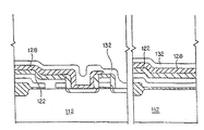
도 3D를 참조하면, 기판(112) 상부에 제2 산화물층(128)이 적층된다. 제2 산화물층(128)은 패터닝되고 에칭되어 메모리 셀 어레이 내 접지 라인(도시되지 않음) 및 비트 라인 콘택 랜딩 패드(130)(도 3E 참조)의 원하는 위치에 기판(112)을 노출시킨다. 선택적으로, 주변부의 제2 산화물층(128)이 제거된다. 기판(112)의 상부에 제2 폴리실리콘층(132)이 적층된다. 도 3E를 참조하면, 제2 폴리실리콘층(132)이 패터닝되고 에칭되어 메모리 셀 어레이 내에 접지 라인(도시되지 않음) 및 비트 라인 콘택 랜딩 패드(130)가 형성되며 주변부로부터 제2 폴리실리콘층(132)이 제거된다.Referring to FIG. 3D, a
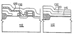
도 3F를 참조하면, 기판(112) 상부에 제3 산화물층(134)이 적층된다. 제3, 제2 및 제1 산화물층들(134, 128, 122)이 패터닝되고 에칭되어 어레이 내에 노출 콘택 영역(136)이 형성되고 주변부들로부터는 이들 층들이 제거된다. 그 다음, 기판(112) 상부에 제3 폴리실리콘층(138)이 적층된다. 어레이 내 제3 폴리실리콘층(138)이 패터닝되고 에칭되어 부하 저항(106)의 형성이 완료된다. 바람직한 실시예에서, 이러한 에칭은 주변부에서 사용되어 폴리실리콘층들(120, 116)을 통해 에칭을 계속함으로써 주변 p 채널 트랜지스터 게이트(140)가 형성된다. 주변부에서의 폴리실리콘층들의 연속 에칭시 제3 산화물층(134)은 어레이 내 하부 소자들의 적절한 보호를 제공한다. 또한, 주변부는 독립적으로 패터닝되고 에칭되어 주변 p 채널 트랜지스터 게이트(140)가 형성될 수 있다. 그 다음, 주변 p 채널 트랜지스터 게이트(140)에 인접한 기판(112)에 p형 불순물을 이온 주입함으로써 주변부에 소스/드레인 영역(142)이 형성되며, 따라서 주변 p 채널 트랜지스터(108)의 형성이 완료된다. 최상부 폴리실리콘층이 접지 라인 및 비트 라인 콘택 랜딩 패드(p 채널 부하 트랜지스터를 구비한 6 트랜지스터 SRAM의 경우)를 형성하는 SRAM 구조에서는 접지 라인 및 비트 라인 랜딩 패드를 형성하는 데 사용되는 동일 패터닝 및 에칭 단계시에 주변 p 채널 트랜지스터 게이트가 형성된다.Referring to FIG. 3F, a
도 2를 다시 참조하면, 그 다음, 전에 형성된 구조의 노출 상부면 위헤 두께운 산화물층(143) 및 보로포스포러스 실리케이트 글래스(BPSG)층(144)이 형성된다. BPSG층(144) 및 두꺼운 산화물층(143)이 패터닝되고 에칭되어 금속 기둥(146)을 위한 개구가 형성된다. 금속 기둥(146) 및 비트 라인(148)은 당해 분야에 잘 알려진 금속 침적 기술을 사용하여 형성된다.Referring again to FIG. 2, a
도 4A-4F에 도시된 본 발명의 다른 실시예에서는 주변 p 채널 트랜지스터 게이트(140)는 비트 라인 랜딩 패드(130)의 형성과 동시에 형성된다. 편리를 위해 도 4A-4F에 사용되는 참조 부호들은 도 2 및 3A-3F의 바람직한 실시예에 사용된 것과 동일하다. 도 4A를 참조하면, 기판(112)이 산화되어 게이트 산화물층(114) 및 두꺼운 필드 산화물 영역(114)이 형성된다. 선택 폴리실리콘층(116)이 게이트 산화물층(114)의 상부에 형성된다. 선택 폴리실리콘층(116)이 패터닝되고 에칭되어 매몰 콘택(118)의 원하는 위치에 기판(112)의 일부가 노출된다. 제1 폴리실리콘층(120)이 선택 폴리실리콘층(116) 및 기판(112)의 노출부 상부에 형성된다.In another embodiment of the invention shown in FIGS. 4A-4F, the peripheral p-
도 4B를 참조하면, 메모리 셀 어레이 내 폴리실리콘층들(120, 116)이 패터닝되고 에칭되어 액세스 트랜지스터 게이트(123)가 형성되고 액세스 트랜지스터(104)의 원하는 소스/드레인 영역의 위치에 기판이 노출된다. 기판(112)의 노출부에 n형 불순물을 이온 주입함으로써 저농도 드레인(LDD)이 형성된다. 그 다음, 전에 에칭된 폴리실리콘층의 측벽상에 산화물 스페이서(126)가 형성된다. LDD 형성시 사용된 것보다 높은 이온 주입 농도로 기판(112)의 나머지 노출부에 불순물을 이온 주입함으로써 소스/드레인 영역의 형성(124)이 완료된다.Referring to FIG. 4B, the polysilicon layers 120, 116 in the memory cell array are patterned and etched to form an
도 4C 및 4D를 참조하면, 기판(112) 상부에 산화물층(128)이 적층된다. 산화물층(128)은 패터닝되고 에칭되어 메모리 셀 어레이 내 비트 라인 콘택 랜딩 패드(130)의 원하는 위치에 기판(112)이 노출되며, 주변부의 산화물층(128)이 제거된다. 기판(112)의 상부에 제2 폴리실리콘층(132)이 적층되고 제2 폴리실리콘층(132)이 패터닝되고 에칭되어 메모리 셀 어레이 내에 비트 라인 콘택 랜딩 패드(130)가 형성된다. 주변부의 폴리실리콘층들(132, 120, 116)이 동시에 에칭되어 주변 p 채널 게이트(140)가 형성된다.4C and 4D, an
도 4E를 참조하면, 기판(112) 상부에 산화물층(134)이 적층된다. 산화물층들(134, 128)이 패터닝되고 에칭되어 어레이 내에 노출 콘택 영역(136)이 형성되고 주변부에 산화물 캡(cap)(139)이 형성된다. 그 다음, 기판(112) 상부에 제3 폴리실리콘층(138)이 적층된다. 어레이 내의 제3 폴리실리콘층(138)이 패터닝되고 에칭되어 부하 저항의 형성이 완료된다. 동시에 주변부로부터 제3 폴리실리콘층(138)이 제거된다. 그 다음, 주변 p 채널 트랜지스터 게이트(140)에 인접한 기판(112)에 p형 불순물을 이온 주입함으로써 주변부에 소스/드레인 영역(142)이 형성되며, 따라서 주변 p 채널 트랜지스터(108)의 형성이 완료된다.Referring to FIG. 4E, an
그 다음, 바람직한 실시예에서 설명되고 도 4F에 도시된 바와 같이 장치의 형성이 완료된다.Then, the formation of the device is completed as described in the preferred embodiment and shown in FIG. 4F.
이제, 도 5를 참조하면, DRAM 메모리 셀 어레이 내 액세스 트랜지스터(10) 및 커패시터(12)를 포함하는 하나의 메모리 셀이 좌측에 도시되어 있고 주변 회로 내 하나의 주변 p 채널 트랜지스터(14)가 우측에 도시되어 있다. 이제, 도 4에 도시된 장치의 형성 공정이 도 6A-6F를 참조하여 설명된다.Referring now to FIG. 5, one memory cell comprising an
도 6A를 참조하면, p형 단결정 실리콘 기판(18)이 산화되어 게이트 산화물층(20) 및 두꺼운 필드 산화물 영역(16)이 형성된다. 필드 산화물 영역(16)은 메모리 셀 어레이와 주변부 사이 및 어레이 내 개별 메모리 셀들 간의 전기적 절연을 제공한다. 게이트 산화물층(20) 상부에 화학 기상 침적(CVD) 방식으로 제1 폴리실리콘층(22)이 형성된다.Referring to FIG. 6A, the p-type single
도 6B를 참조하면, 어레이 내의 제1 폴리실리콘층(22)이 패터닝되고 에칭되어 액세스 트랜지스터(10)의 게이트(24)(워드 라인 26A) 및 워드 라인(26B)이 형성된다. 그 다음, 기판(18)의 표면에 불순물이 이온 주입되어 소스/드레인 영역(28, 30)이 형성된다. 도 6C를 참조하면, 기판(18) 상부에 제2 산화물층이(32)이 적층된다. 어레이 내의 제2 산화물층(32)이 패터닝되고 에칭되어 소스/드레인 영역(28)에 매몰 콘택 영역(34)이 형성되고, 소스/드레인 영역(30)에 비트 라인 콘택(36)이 형성되며, 게이트(24)와 워드 라인(26B)에 인접하게 측벽(38)이 형성된다. 이러한 에칭의 일부로서, 주변부로부터 제2 산화물층(32)이 제거된다. 도 6D를 참조하면, 기판(18) 상부에 제2 폴리실리콘층(39)이 적층된다. 어레이 내의 제2 폴리실리콘층(39)이 패터닝되고 에칭되어 커패시터(12)의 하부 전극(42)이 형성된다. 주변부에서 폴리실리콘층들(39, 22)이 동시에 에칭되어 주변 p 채널 트랜지스터 게이트(50)가 형성된다. 주변 p 채널 트랜지스터 게이트(50)에 인접한 기판(18) 표면에 불순물이 이온 주입되어 소스/드레인 영역(52)이 형성되며, 따라서 주변 p 채널 트랜지스터(14)의 형성이 완료된다. 하부 전극(42)은 소스/드레인 영역(28)을 따라 접촉한 상태로 게이트(24)로부터 워드 라인(26B)까지 연장된다. 그 다음, 하부 전극(42) 상부에 유전층(44)이 형성된다. 유전층(44)은 질화물 박막, 산화물-질화물-산화물(ONO)막 또는 다른 적절한 물질로 이루어진다. 그 다음, 도 6E에 도시된 바와 같이, 기판(18) 상부에 제3 폴리실리콘층(46)이 적층된다.Referring to FIG. 6B, the
도 6E 및6F를 참조하면, 제3 폴리실리콘층(46)이 패터닝되고 에칭되어 어레이 내에 상부 전극(48)이 형성되고 주변부로부터 제3 폴리실리콘층(46) 및 유전층(44)이 제거된다.6E and 6F, the
다시 도 4를 참조하면, 전에 형성된 구조의 노출 상부면 위에 두꺼운 BPSG층(56) 또는 다른 적절한 절연체가 형성된다. BPSG층(56)이 패터닝되고 에칭되어 금속 기둥(58)을 위한 개구가 형성된다. 금속 기둥(58) 및 비트 라인(60)은 당해 분야에 잘 알려진 금속 침적 기술을 사용하여 형성된다.Referring again to FIG. 4, a
전술한 본 발명의 바람직한 실시예들의 각종 변형 및 응용이 가능하다. 예컨대, 본 발명은 다른 메모리 셀/주변 회로 장치들 및 구조들의 형성에 사용될 수 있으며, 공정 단계 및 물질에 대한 변형이 이루어질 수 있다. 따라서, 본 발명은 첨부된 청구 범위에 의해서만 제한된다.Various modifications and applications of the above-described preferred embodiments of the present invention are possible. For example, the present invention can be used to form other memory cell / peripheral circuit devices and structures, and modifications to processing steps and materials can be made. Accordingly, the invention is limited only by the appended claims.
Claims (13)
Applications Claiming Priority (2)
| Application Number | Priority Date | Filing Date | Title |
|---|---|---|---|
| US37610395A | 1995-01-19 | 1995-01-19 | |
| US8/376103 | 1995-01-19 |
Publications (2)
| Publication Number | Publication Date |
|---|---|
| KR19980701531A KR19980701531A (en) | 1998-05-15 |
| KR100246162B1 true KR100246162B1 (en) | 2000-03-15 |
Family
ID=23483721
Family Applications (1)
| Application Number | Title | Priority Date | Filing Date |
|---|---|---|---|
| KR1019970704922A Expired - Fee Related KR100246162B1 (en) | 1995-01-19 | 1996-01-19 | How to Form a Transistor in a Peripheral Circuit |
Country Status (6)
| Country | Link |
|---|---|
| US (3) | US6040209A (en) |
| EP (1) | EP0804805B1 (en) |
| JP (1) | JP3261435B2 (en) |
| KR (1) | KR100246162B1 (en) |
| DE (1) | DE69623440T2 (en) |
| WO (1) | WO1996022612A1 (en) |
Cited By (1)
| Publication number | Priority date | Publication date | Assignee | Title |
|---|---|---|---|---|
| KR20210016641A (en) * | 2018-08-23 | 2021-02-16 | 마이크론 테크놀로지, 인크 | Integrated circuit configuration |
Families Citing this family (8)
| Publication number | Priority date | Publication date | Assignee | Title |
|---|---|---|---|---|
| US7064376B2 (en) * | 1996-05-24 | 2006-06-20 | Jeng-Jye Shau | High performance embedded semiconductor memory devices with multiple dimension first-level bit-lines |
| US20050036363A1 (en) * | 1996-05-24 | 2005-02-17 | Jeng-Jye Shau | High performance embedded semiconductor memory devices with multiple dimension first-level bit-lines |
| US5748547A (en) * | 1996-05-24 | 1998-05-05 | Shau; Jeng-Jye | High performance semiconductor memory devices having multiple dimension bit lines |
| EP0923116A1 (en) * | 1997-12-12 | 1999-06-16 | STMicroelectronics S.r.l. | Process for manufacturing integrated multi-crystal silicon resistors in MOS technology and integrated MOS device comprising multi-crystal silicon resistors |
| TW582095B (en) * | 2003-04-10 | 2004-04-01 | Nanya Technology Corp | Bit line contact and method for forming the same |
| KR100487563B1 (en) * | 2003-04-30 | 2005-05-03 | 삼성전자주식회사 | Semiconductor device and method of forming the same |
| US7208369B2 (en) * | 2003-09-15 | 2007-04-24 | Taiwan Semiconductor Manufacturing Company, Ltd. | Dual poly layer and method of manufacture |
| KR100701697B1 (en) * | 2005-06-29 | 2007-03-29 | 주식회사 하이닉스반도체 | Manufacturing method of CMOS device having dual polyside gate |
Family Cites Families (22)
| Publication number | Priority date | Publication date | Assignee | Title |
|---|---|---|---|---|
| JPS53124084A (en) * | 1977-04-06 | 1978-10-30 | Hitachi Ltd | Semiconductor memory device containing floating type poly silicon layer and its manufacture |
| US4408385A (en) * | 1978-06-15 | 1983-10-11 | Texas Instruments Incorporated | Semiconductor integrated circuit with implanted resistor element in polycrystalline silicon layer |
| US4370798A (en) * | 1979-06-15 | 1983-02-01 | Texas Instruments Incorporated | Interlevel insulator for integrated circuit with implanted resistor element in second-level polycrystalline silicon |
| US5352620A (en) * | 1984-05-23 | 1994-10-04 | Hitachi, Ltd. | Method of making semiconductor device with memory cells and peripheral transistors |
| EP0272433B1 (en) * | 1986-11-18 | 1993-03-31 | Siemens Aktiengesellschaft | Integrated semiconductor circuit having load resistors arranged as thin-film bars in the field oxide regions separating the active transistor regions, and process for their manufacture |
| JPH02122563A (en) * | 1988-10-31 | 1990-05-10 | Nec Corp | Manufacturing method of semiconductor device |
| JPH03259566A (en) * | 1990-02-02 | 1991-11-19 | Sony Corp | Manufacture of memory device |
| US5281838A (en) | 1990-03-13 | 1994-01-25 | Mitsubishi Denki Kabushiki Kaisha | Semiconductor device having contact between wiring layer and impurity region |
| US5276344A (en) * | 1990-04-27 | 1994-01-04 | Mitsubishi Denki Kabushiki Kaisha | Field effect transistor having impurity regions of different depths and manufacturing method thereof |
| JPH0834304B2 (en) * | 1990-09-20 | 1996-03-29 | 富士通株式会社 | Semiconductor device and manufacturing method thereof |
| JP2666549B2 (en) * | 1990-09-27 | 1997-10-22 | 日本電気株式会社 | Semiconductor memory device and method of manufacturing the same |
| JPH04165670A (en) * | 1990-10-30 | 1992-06-11 | Toshiba Corp | Semiconductor memory and manufacture thereof |
| JPH04186877A (en) * | 1990-11-21 | 1992-07-03 | Fujitsu Ltd | Manufacture of semiconductor device |
| JPH04322459A (en) * | 1991-04-23 | 1992-11-12 | Nec Corp | Semiconductor memory device and manufacture thereof |
| US5327002A (en) | 1991-05-15 | 1994-07-05 | Kawasaki Steel Corporation | SRAM with gate oxide films of varied thickness |
| JPH0521805A (en) * | 1991-07-10 | 1993-01-29 | Fujitsu Ltd | Method for manufacturing semiconductor device |
| JPH05121700A (en) * | 1991-08-28 | 1993-05-18 | Fujitsu Ltd | Semiconductor device and manufacturing method thereof |
| JP3548984B2 (en) * | 1991-11-14 | 2004-08-04 | 富士通株式会社 | Method for manufacturing semiconductor device |
| JP2705476B2 (en) * | 1992-08-07 | 1998-01-28 | ヤマハ株式会社 | Method for manufacturing semiconductor device |
| US5500387A (en) * | 1994-02-16 | 1996-03-19 | Texas Instruments Incorporated | Method of making high performance capacitors and/or resistors for integrated circuits |
| JPH09270461A (en) * | 1996-03-29 | 1997-10-14 | Mitsubishi Electric Corp | Semiconductor device |
| US5808335A (en) * | 1996-06-13 | 1998-09-15 | Vanguard International Semiconductor Corporation | Reduced mask DRAM process |
-
1996
- 1996-01-19 WO PCT/US1996/000615 patent/WO1996022612A1/en not_active Ceased
- 1996-01-19 KR KR1019970704922A patent/KR100246162B1/en not_active Expired - Fee Related
- 1996-01-19 EP EP96904473A patent/EP0804805B1/en not_active Expired - Lifetime
- 1996-01-19 JP JP52236696A patent/JP3261435B2/en not_active Expired - Fee Related
- 1996-01-19 DE DE69623440T patent/DE69623440T2/en not_active Expired - Lifetime
-
1997
- 1997-01-21 US US08/786,175 patent/US6040209A/en not_active Expired - Fee Related
-
1998
- 1998-10-14 US US09/173,038 patent/US6252268B1/en not_active Expired - Fee Related
-
1999
- 1999-12-07 US US09/456,140 patent/US6271073B1/en not_active Expired - Fee Related
Cited By (2)
| Publication number | Priority date | Publication date | Assignee | Title |
|---|---|---|---|---|
| KR20210016641A (en) * | 2018-08-23 | 2021-02-16 | 마이크론 테크놀로지, 인크 | Integrated circuit configuration |
| KR102359065B1 (en) | 2018-08-23 | 2022-02-08 | 마이크론 테크놀로지, 인크 | integrated circuit construction |
Also Published As
| Publication number | Publication date |
|---|---|
| JPH10505712A (en) | 1998-06-02 |
| US6040209A (en) | 2000-03-21 |
| US6252268B1 (en) | 2001-06-26 |
| WO1996022612A1 (en) | 1996-07-25 |
| DE69623440T2 (en) | 2003-08-07 |
| DE69623440D1 (en) | 2002-10-10 |
| EP0804805A1 (en) | 1997-11-05 |
| US6271073B1 (en) | 2001-08-07 |
| EP0804805B1 (en) | 2002-09-04 |
| JP3261435B2 (en) | 2002-03-04 |
| KR19980701531A (en) | 1998-05-15 |
Similar Documents
| Publication | Publication Date | Title |
|---|---|---|
| US8629533B2 (en) | Pillars for vertical transistors | |
| US4075045A (en) | Method for fabricating FET one-device memory cells with two layers of polycrystalline silicon and fabrication of integrated circuits containing arrays of the memory cells charge storage capacitors utilizing five basic pattern deliberating steps | |
| US4183040A (en) | MOS RAM with implant forming peripheral depletion MOSFET channels and capacitor bottom electrodes | |
| US4095251A (en) | Field effect transistors and fabrication of integrated circuits containing the transistors | |
| KR0128826B1 (en) | DRAM cell manufacturing method | |
| KR100246162B1 (en) | How to Form a Transistor in a Peripheral Circuit | |
| US5283204A (en) | Method of forming passivation oxidation for improving cell leakage and cell area | |
| US6479355B2 (en) | Method for forming landing pad | |
| US6080609A (en) | Method of making MOSFET structure | |
| KR930015002A (en) | Semiconductor memory device and manufacturing method thereof | |
| JPH04216665A (en) | Semiconductor memory element and its manufacture | |
| US5691221A (en) | Method for manufacturing semiconductor memory device having a stacked capacitor | |
| KR100390891B1 (en) | Manufacturing method of highly integrated semiconductor device | |
| KR0169599B1 (en) | Semiconductor device and manufacturing method | |
| KR970011758B1 (en) | A method for fabricating dram cells | |
| KR100281038B1 (en) | Semiconductor Memory Device Manufacturing Method | |
| KR100223895B1 (en) | DRAM cell and manufacturing method thereof | |
| KR0156169B1 (en) | Method of manufacturing semiconductor memory | |
| KR0131741B1 (en) | Semiconductor memory device and manufacturing method thereof | |
| KR930009589B1 (en) | Method for manufacturing a capacitor of lsi mos device | |
| KR0126114B1 (en) | The manufacturing method for semiconductor memory device | |
| KR19990005489A (en) | Semiconductor device manufacturing method | |
| KR20000041808A (en) | Method for manufacturing capacitor of semiconductor device | |
| KR19990003042A (en) | Capacitor Formation Method of Semiconductor Device | |
| KR19980026302A (en) | Manufacturing Method of Semiconductor Memory Device |
Legal Events
| Date | Code | Title | Description |
|---|---|---|---|
| A201 | Request for examination | ||
| PA0105 | International application |
St.27 status event code: A-0-1-A10-A15-nap-PA0105 |
|
| PA0201 | Request for examination |
St.27 status event code: A-1-2-D10-D11-exm-PA0201 |
|
| R17-X000 | Change to representative recorded |
St.27 status event code: A-3-3-R10-R17-oth-X000 |
|
| PG1501 | Laying open of application |
St.27 status event code: A-1-1-Q10-Q12-nap-PG1501 |
|
| R18-X000 | Changes to party contact information recorded |
St.27 status event code: A-3-3-R10-R18-oth-X000 |
|
| PN2301 | Change of applicant |
St.27 status event code: A-3-3-R10-R13-asn-PN2301 St.27 status event code: A-3-3-R10-R11-asn-PN2301 |
|
| R18-X000 | Changes to party contact information recorded |
St.27 status event code: A-3-3-R10-R18-oth-X000 |
|
| E701 | Decision to grant or registration of patent right | ||
| PE0701 | Decision of registration |
St.27 status event code: A-1-2-D10-D22-exm-PE0701 |
|
| GRNT | Written decision to grant | ||
| PR0701 | Registration of establishment |
St.27 status event code: A-2-4-F10-F11-exm-PR0701 |
|
| PR1002 | Payment of registration fee |
St.27 status event code: A-2-2-U10-U12-oth-PR1002 Fee payment year number: 1 |
|
| PG1601 | Publication of registration |
St.27 status event code: A-4-4-Q10-Q13-nap-PG1601 |
|
| PR1001 | Payment of annual fee |
St.27 status event code: A-4-4-U10-U11-oth-PR1001 Fee payment year number: 4 |
|
| PR1001 | Payment of annual fee |
St.27 status event code: A-4-4-U10-U11-oth-PR1001 Fee payment year number: 5 |
|
| PR1001 | Payment of annual fee |
St.27 status event code: A-4-4-U10-U11-oth-PR1001 Fee payment year number: 6 |
|
| PR1001 | Payment of annual fee |
St.27 status event code: A-4-4-U10-U11-oth-PR1001 Fee payment year number: 7 |
|
| PR1001 | Payment of annual fee |
St.27 status event code: A-4-4-U10-U11-oth-PR1001 Fee payment year number: 8 |
|
| PR1001 | Payment of annual fee |
St.27 status event code: A-4-4-U10-U11-oth-PR1001 Fee payment year number: 9 |
|
| PR1001 | Payment of annual fee |
St.27 status event code: A-4-4-U10-U11-oth-PR1001 Fee payment year number: 10 |
|
| PR1001 | Payment of annual fee |
St.27 status event code: A-4-4-U10-U11-oth-PR1001 Fee payment year number: 11 |
|
| FPAY | Annual fee payment |
Payment date: 20101124 Year of fee payment: 12 |
|
| PR1001 | Payment of annual fee |
St.27 status event code: A-4-4-U10-U11-oth-PR1001 Fee payment year number: 12 |
|
| R18-X000 | Changes to party contact information recorded |
St.27 status event code: A-5-5-R10-R18-oth-X000 |
|
| LAPS | Lapse due to unpaid annual fee | ||
| PC1903 | Unpaid annual fee |
St.27 status event code: A-4-4-U10-U13-oth-PC1903 Not in force date: 20111204 Payment event data comment text: Termination Category : DEFAULT_OF_REGISTRATION_FEE |
|
| PC1903 | Unpaid annual fee |
St.27 status event code: N-4-6-H10-H13-oth-PC1903 Ip right cessation event data comment text: Termination Category : DEFAULT_OF_REGISTRATION_FEE Not in force date: 20111204 |
|
| P22-X000 | Classification modified |
St.27 status event code: A-4-4-P10-P22-nap-X000 |
|
| P22-X000 | Classification modified |
St.27 status event code: A-4-4-P10-P22-nap-X000 |
|
| P22-X000 | Classification modified |
St.27 status event code: A-4-4-P10-P22-nap-X000 |