KR100281147B1 - 콘택홀 형성방법 - Google Patents
콘택홀 형성방법 Download PDFInfo
- Publication number
- KR100281147B1 KR100281147B1 KR1019970050956A KR19970050956A KR100281147B1 KR 100281147 B1 KR100281147 B1 KR 100281147B1 KR 1019970050956 A KR1019970050956 A KR 1019970050956A KR 19970050956 A KR19970050956 A KR 19970050956A KR 100281147 B1 KR100281147 B1 KR 100281147B1
- Authority
- KR
- South Korea
- Prior art keywords
- forming
- contact hole
- insulating film
- nitride film
- film
- Prior art date
- Legal status (The legal status is an assumption and is not a legal conclusion. Google has not performed a legal analysis and makes no representation as to the accuracy of the status listed.)
- Expired - Fee Related
Links
Images




Classifications
-
- H—ELECTRICITY
- H10—SEMICONDUCTOR DEVICES; ELECTRIC SOLID-STATE DEVICES NOT OTHERWISE PROVIDED FOR
- H10W—GENERIC PACKAGES, INTERCONNECTIONS, CONNECTORS OR OTHER CONSTRUCTIONAL DETAILS OF DEVICES COVERED BY CLASS H10
- H10W20/00—Interconnections in chips, wafers or substrates
- H10W20/01—Manufacture or treatment
- H10W20/071—Manufacture or treatment of dielectric parts thereof
- H10W20/081—Manufacture or treatment of dielectric parts thereof by forming openings in the dielectric parts
-
- H—ELECTRICITY
- H10—SEMICONDUCTOR DEVICES; ELECTRIC SOLID-STATE DEVICES NOT OTHERWISE PROVIDED FOR
- H10P—GENERIC PROCESSES OR APPARATUS FOR THE MANUFACTURE OR TREATMENT OF DEVICES COVERED BY CLASS H10
- H10P50/00—Etching of wafers, substrates or parts of devices
- H10P50/20—Dry etching; Plasma etching; Reactive-ion etching
- H10P50/28—Dry etching; Plasma etching; Reactive-ion etching of insulating materials
- H10P50/282—Dry etching; Plasma etching; Reactive-ion etching of insulating materials of inorganic materials
-
- H—ELECTRICITY
- H10—SEMICONDUCTOR DEVICES; ELECTRIC SOLID-STATE DEVICES NOT OTHERWISE PROVIDED FOR
- H10P—GENERIC PROCESSES OR APPARATUS FOR THE MANUFACTURE OR TREATMENT OF DEVICES COVERED BY CLASS H10
- H10P50/00—Etching of wafers, substrates or parts of devices
- H10P50/20—Dry etching; Plasma etching; Reactive-ion etching
- H10P50/28—Dry etching; Plasma etching; Reactive-ion etching of insulating materials
- H10P50/286—Dry etching; Plasma etching; Reactive-ion etching of insulating materials of organic materials
-
- H—ELECTRICITY
- H10—SEMICONDUCTOR DEVICES; ELECTRIC SOLID-STATE DEVICES NOT OTHERWISE PROVIDED FOR
- H10P—GENERIC PROCESSES OR APPARATUS FOR THE MANUFACTURE OR TREATMENT OF DEVICES COVERED BY CLASS H10
- H10P50/00—Etching of wafers, substrates or parts of devices
- H10P50/73—Etching of wafers, substrates or parts of devices using masks for insulating materials
-
- H—ELECTRICITY
- H10—SEMICONDUCTOR DEVICES; ELECTRIC SOLID-STATE DEVICES NOT OTHERWISE PROVIDED FOR
- H10W—GENERIC PACKAGES, INTERCONNECTIONS, CONNECTORS OR OTHER CONSTRUCTIONAL DETAILS OF DEVICES COVERED BY CLASS H10
- H10W20/00—Interconnections in chips, wafers or substrates
- H10W20/01—Manufacture or treatment
- H10W20/031—Manufacture or treatment of conductive parts of the interconnections
- H10W20/056—Manufacture or treatment of conductive parts of the interconnections by filling conductive material into holes, grooves or trenches
-
- H—ELECTRICITY
- H10—SEMICONDUCTOR DEVICES; ELECTRIC SOLID-STATE DEVICES NOT OTHERWISE PROVIDED FOR
- H10W—GENERIC PACKAGES, INTERCONNECTIONS, CONNECTORS OR OTHER CONSTRUCTIONAL DETAILS OF DEVICES COVERED BY CLASS H10
- H10W20/00—Interconnections in chips, wafers or substrates
- H10W20/01—Manufacture or treatment
- H10W20/031—Manufacture or treatment of conductive parts of the interconnections
- H10W20/062—Manufacture or treatment of conductive parts of the interconnections by smoothing of conductive parts, e.g. by planarisation
Landscapes
- Internal Circuitry In Semiconductor Integrated Circuit Devices (AREA)
Abstract
Description
Claims (1)
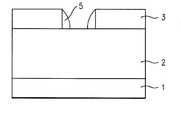
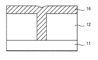
- 기판에 층간절연층을 증착하는 공정과,상기 층간절연층상에 소정부분이 식각된 질화막을 형성하는 공정과,소정부분 식각된 상기 절연막의 측면에 측벽질화막을 형성하는 공정과,상기 질화막과 측벽질화막을 마스크로 상기 층간절연층을 식각하여 콘택홀을 형성하는 공정과,상기 질화막과 측벽질화막을 제거하는 공정과,상기 콘택홀에 플러그를 형성하는 것을 포함함을 특징으로 하는 콘택홀 형성방법.
Priority Applications (1)
| Application Number | Priority Date | Filing Date | Title |
|---|---|---|---|
| KR1019970050956A KR100281147B1 (ko) | 1997-10-02 | 1997-10-02 | 콘택홀 형성방법 |
Applications Claiming Priority (1)
| Application Number | Priority Date | Filing Date | Title |
|---|---|---|---|
| KR1019970050956A KR100281147B1 (ko) | 1997-10-02 | 1997-10-02 | 콘택홀 형성방법 |
Publications (2)
| Publication Number | Publication Date |
|---|---|
| KR19990030645A KR19990030645A (ko) | 1999-05-06 |
| KR100281147B1 true KR100281147B1 (ko) | 2001-04-02 |
Family
ID=66045072
Family Applications (1)
| Application Number | Title | Priority Date | Filing Date |
|---|---|---|---|
| KR1019970050956A Expired - Fee Related KR100281147B1 (ko) | 1997-10-02 | 1997-10-02 | 콘택홀 형성방법 |
Country Status (1)
| Country | Link |
|---|---|
| KR (1) | KR100281147B1 (ko) |
Citations (1)
| Publication number | Priority date | Publication date | Assignee | Title |
|---|---|---|---|---|
| JPH08148565A (ja) * | 1994-11-22 | 1996-06-07 | Hitachi Ltd | 半導体集積回路装置の製造方法 |
-
1997
- 1997-10-02 KR KR1019970050956A patent/KR100281147B1/ko not_active Expired - Fee Related
Patent Citations (1)
| Publication number | Priority date | Publication date | Assignee | Title |
|---|---|---|---|---|
| JPH08148565A (ja) * | 1994-11-22 | 1996-06-07 | Hitachi Ltd | 半導体集積回路装置の製造方法 |
Also Published As
| Publication number | Publication date |
|---|---|
| KR19990030645A (ko) | 1999-05-06 |
Similar Documents
| Publication | Publication Date | Title |
|---|---|---|
| US6420257B2 (en) | Process for forming trenches and contacts during the formation of a semiconductor memory device | |
| JPH01290236A (ja) | 幅の広いトレンチを平坦化する方法 | |
| JPH09181180A (ja) | 半導体集積回路及びその製造方法 | |
| JP4057083B2 (ja) | 半導体集積回路の製造方法 | |
| US5854126A (en) | Method for forming metallization in semiconductor devices with a self-planarizing material | |
| KR100281147B1 (ko) | 콘택홀 형성방법 | |
| KR100449319B1 (ko) | 반도체 소자의 미세 패턴 형성 방법 | |
| KR100304979B1 (ko) | 반도체소자의배선형성방법 | |
| US6284645B1 (en) | Controlling improvement of critical dimension of dual damasceue process using spin-on-glass process | |
| KR100306905B1 (ko) | 접촉홀형성방법 | |
| KR100406582B1 (ko) | 도전 플러그 형성 방법 | |
| KR0124638B1 (ko) | 반도체장치의 다층배선 형성방법 | |
| JPH11145285A (ja) | 配線形成方法 | |
| KR100356478B1 (ko) | 반도체 소자의 게이트 전극 형성 방법 | |
| KR0172249B1 (ko) | 반도체소자의 콘택홀 형성방법 | |
| KR20010047961A (ko) | 산화막 마스크를 사용하는 라인 퍼스트 듀얼 다마신 패턴형성방법 | |
| KR100247642B1 (ko) | 반도체 소자의 콘택홀 형성방법 | |
| KR20030052664A (ko) | 나노 크기의 금속 배선 패턴 형성 방법 | |
| KR20010060984A (ko) | 반도체 장치의 콘택홀 형성방법 | |
| KR100328824B1 (ko) | 커패시터 제조방법 | |
| KR100252873B1 (ko) | 반도체 소자의 다층배선 및 그의 형성방법 | |
| KR20020002932A (ko) | 반도체소자의 게이트전극 형성방법 | |
| KR20010009868A (ko) | 반도체소자의 홀 형성방법 | |
| KR19980058461A (ko) | 반도체 소자의 제조방법 | |
| KR20030002081A (ko) | 이중 습식식각을 이용한 콘택홀 형성방법 |
Legal Events
| Date | Code | Title | Description |
|---|---|---|---|
| A201 | Request for examination | ||
| PA0109 | Patent application |
St.27 status event code: A-0-1-A10-A12-nap-PA0109 |
|
| PA0201 | Request for examination |
St.27 status event code: A-1-2-D10-D11-exm-PA0201 |
|
| R17-X000 | Change to representative recorded |
St.27 status event code: A-3-3-R10-R17-oth-X000 |
|
| PG1501 | Laying open of application |
St.27 status event code: A-1-1-Q10-Q12-nap-PG1501 |
|
| PN2301 | Change of applicant |
St.27 status event code: A-3-3-R10-R13-asn-PN2301 St.27 status event code: A-3-3-R10-R11-asn-PN2301 |
|
| E902 | Notification of reason for refusal | ||
| PE0902 | Notice of grounds for rejection |
St.27 status event code: A-1-2-D10-D21-exm-PE0902 |
|
| E601 | Decision to refuse application | ||
| PE0601 | Decision on rejection of patent |
St.27 status event code: N-2-6-B10-B15-exm-PE0601 |
|
| AMND | Amendment | ||
| J201 | Request for trial against refusal decision | ||
| P11-X000 | Amendment of application requested |
St.27 status event code: A-2-2-P10-P11-nap-X000 |
|
| P13-X000 | Application amended |
St.27 status event code: A-2-2-P10-P13-nap-X000 |
|
| PJ0201 | Trial against decision of rejection |
St.27 status event code: A-3-3-V10-V11-apl-PJ0201 |
|
| PB0901 | Examination by re-examination before a trial |
St.27 status event code: A-6-3-E10-E12-rex-PB0901 |
|
| B701 | Decision to grant | ||
| PB0701 | Decision of registration after re-examination before a trial |
St.27 status event code: A-3-4-F10-F13-rex-PB0701 |
|
| GRNT | Written decision to grant | ||
| PR0701 | Registration of establishment |
St.27 status event code: A-2-4-F10-F11-exm-PR0701 |
|
| PR1002 | Payment of registration fee |
St.27 status event code: A-2-2-U10-U11-oth-PR1002 Fee payment year number: 1 |
|
| PG1601 | Publication of registration |
St.27 status event code: A-4-4-Q10-Q13-nap-PG1601 |
|
| PR1001 | Payment of annual fee |
St.27 status event code: A-4-4-U10-U11-oth-PR1001 Fee payment year number: 4 |
|
| PR1001 | Payment of annual fee |
St.27 status event code: A-4-4-U10-U11-oth-PR1001 Fee payment year number: 5 |
|
| PR1001 | Payment of annual fee |
St.27 status event code: A-4-4-U10-U11-oth-PR1001 Fee payment year number: 6 |
|
| PR1001 | Payment of annual fee |
St.27 status event code: A-4-4-U10-U11-oth-PR1001 Fee payment year number: 7 |
|
| PR1001 | Payment of annual fee |
St.27 status event code: A-4-4-U10-U11-oth-PR1001 Fee payment year number: 8 |
|
| FPAY | Annual fee payment |
Payment date: 20081027 Year of fee payment: 9 |
|
| PR1001 | Payment of annual fee |
St.27 status event code: A-4-4-U10-U11-oth-PR1001 Fee payment year number: 9 |
|
| LAPS | Lapse due to unpaid annual fee | ||
| PC1903 | Unpaid annual fee |
St.27 status event code: A-4-4-U10-U13-oth-PC1903 Not in force date: 20091116 Payment event data comment text: Termination Category : DEFAULT_OF_REGISTRATION_FEE |
|
| PC1903 | Unpaid annual fee |
St.27 status event code: N-4-6-H10-H13-oth-PC1903 Ip right cessation event data comment text: Termination Category : DEFAULT_OF_REGISTRATION_FEE Not in force date: 20091116 |
|
| P22-X000 | Classification modified |
St.27 status event code: A-4-4-P10-P22-nap-X000 |
|
| P22-X000 | Classification modified |
St.27 status event code: A-4-4-P10-P22-nap-X000 |