KR100332011B1 - 어드레스트랜지션검출회로를갖는펄스발생회로 - Google Patents
어드레스트랜지션검출회로를갖는펄스발생회로 Download PDFInfo
- Publication number
- KR100332011B1 KR100332011B1 KR1019970020528A KR19970020528A KR100332011B1 KR 100332011 B1 KR100332011 B1 KR 100332011B1 KR 1019970020528 A KR1019970020528 A KR 1019970020528A KR 19970020528 A KR19970020528 A KR 19970020528A KR 100332011 B1 KR100332011 B1 KR 100332011B1
- Authority
- KR
- South Korea
- Prior art keywords
- signal
- circuit
- gate
- node
- inverter
- Prior art date
- Legal status (The legal status is an assumption and is not a legal conclusion. Google has not performed a legal analysis and makes no representation as to the accuracy of the status listed.)
- Expired - Fee Related
Links
Images


Classifications
-
- G—PHYSICS
- G11—INFORMATION STORAGE
- G11C—STATIC STORES
- G11C8/00—Arrangements for selecting an address in a digital store
-
- H—ELECTRICITY
- H03—ELECTRONIC CIRCUITRY
- H03K—PULSE TECHNIQUE
- H03K5/00—Manipulating of pulses not covered by one of the other main groups of this subclass
- H03K5/153—Arrangements in which a pulse is delivered at the instant when a predetermined characteristic of an input signal is present or at a fixed time interval after this instant
- H03K5/1534—Transition or edge detectors
-
- G—PHYSICS
- G11—INFORMATION STORAGE
- G11C—STATIC STORES
- G11C8/00—Arrangements for selecting an address in a digital store
- G11C8/18—Address timing or clocking circuits; Address control signal generation or management, e.g. for row address strobe [RAS] or column address strobe [CAS] signals
Landscapes
- Engineering & Computer Science (AREA)
- Microelectronics & Electronic Packaging (AREA)
- Physics & Mathematics (AREA)
- Nonlinear Science (AREA)
- Dram (AREA)
- Static Random-Access Memory (AREA)
- Pulse Circuits (AREA)
Abstract
Description
Claims (7)
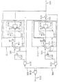
- 펄스 발생 회로에 있어서,입력 신호가 공급되고, 제 1 지연 노드상의 제 1 지연된 신호를 출력하는 지연 회로로서, 상기 제 1 지연된 신호는 상기 입력 신호가 제 2 논리 레벨로부터 제 1 논리 레벨로 변화한 후에 상기 제 1 논리 레벨로부터 상기 제 2 논리 레벨로 변화하는, 상기 지연 회로와,상기 제 1 지연 노드에 연결된 입력을 갖는 제 1 인버터와;상기 입력 신호의 반전된 신호와 상기 제 1 인버터의 출력 신호가 공급되는 제 1 논리 회로로서, 상기 제 1 논리 회로는 상기 반전된 신호와 상기 제 1 인버터의 출력 신호가 모두 상기 제 2 논리 레벨을 취할 매 펄스 신호를 출력하는, 상기 제 1 논리 회로와;상기 제 1 지연 노드와 제 1 전압 라인 사이에 연결된 소스-드레인 경로, 및 상기 입력 신호가 공급되는 게이트를 갖는 제 1 채널형의 제 1 트랜지스터와,상기 반전된 신호가 공급되고, 제 2 지연 노드상의 제 2 지연된 신호를 출력하는 제 2 지연 회로로서, 상기 제 2 지연된 신호는 상기 반전된 신호가 상기 제 2 논리 레벨로부터 상기 제 1 논리 레벨로 변화한 후에 상기 제 1 논리 레벨로부터 상기 제 2 논리 레벨로 변화하는, 상기 제 2 지연 회로와;입력이 상기 제 2 지연 노드에 연결되는 제 2 인버터와;상기 입력 신호와 상기 제 2 인버터의 출력 신호가 공급되는 제 2 논리 회로로서, 상기 제 2 논리 회로는 상기 입력 신호와 상기 제 2 인버터의 출력 신호가 모두 상기 제 2 논리 레벨을 취할 때 제 2 펄스 신호를 출력하는, 상기 제 2 논리회로와;상기 제 2 지연 노드와 상기 제 1 전압 라인 사이에 연결된 소스-드레인 경로와, 상기 반전된 신호가 공급되는 게이트를 갖는 상기 제 1 채널형의 제 2 트랜지스터를 포함하는, 펄스 발생 회로.
- 제 1 항에 있어서,상기 제 2 인버터의 출력 노드와 제 2 전압 라인 사이에 연결된 소스-드레인 경로와, 상기 입력 신호가 공급되는 게이트를 갖는 제 2 채널형의 제 3 트랜지스터를 더 포함하는 펄스 발생 회로.
- 제 1 항에 있어서,상기 제 1 지연 노드와 상기 제 1 전압 라인 사이에 연결된 제 1 커패시터를 더 포함하는 펄스 발생 회로.
- 제 1 항에 있어시,상기 제 2 논리 회로는 NAND 회로인, 펄스 발생 회로.
- 펄스 발생 회로에 있어서,입력 신호의 반전된 신호가 공급되고, 제 1 지연 노드상의 제 1 지연된 신호를 출력하는 지연 회로로서, 상기 제 1 지연된 신호는 상기 반전된 입련 신호가 제 2 논리 레벨로부터 제 1 논리 레벨로 변화한 후에 상기 제 1 논리 레벨로부터 상기 제 2 논리 레벨로 변화하는, 상기 지연 회로와;상기 제 1 지연 노드에 연결된 입력을 갖는 제 1 인버터와;상기 입력 신호와 상기 제 1 인버터의 출력 신호가 공급되는 제 1 논리 회로로서, 상기 제 1 논리 회로는 상기 입력 신호와 상기 제 1 인버터의 상기 출력 신호가 모두 상기 제 2 논리 레벨을 취할 때 펄스 신호를 출력하는, 상기 제 1 논리회로와;상기 제 1 지연 노드와 제 1 전압 라인 사이긴 연결된 소스-드레인 경로와, 상기 입력 신호의 반전된 신호가 공급되는 게이트를 갖는 제 1 채널형의 제 1 트랜지스터와;상기 제 1 인버터의 출력 노드와 제 2 전압 라인 사이에 연결된 소스-드레인 경로와, 상기 입력 신호가 공급되는 게이트를 갖는 제 2 채널형의 제 2 트랜지스터와;상기 입력 신호가 공급되고, 제 2 지연 노드상의 제 2 지연된 신호를 출력하는 제 2 지연 회로로서, 상기 제 2 지연된 신호는 상기 입력 신호가 상기 제 2 논리 레벨로부터 상기 제 1 논리 레벨로 변화한 후에 상기 제 1 논리 레벨로부터 상기 제 2 논리 레벨로 변화하는, 상기 제 2 지연 회로와;입력이 상기 제 2 지연 노드에 연결되는 제 2 인버터와;상기 입력 신호의 반전된 신호와, 상기 제 2 인버터의 출력 신호가 공급되는 제 2 논리 회로로서, 상기 제 2 논리 회로는 상기 반전된 신호와 상기 제 2 인버터의 출력 신호가 모두 상기 제 2 논리 레벨을 취할 때 제 2 펄스 신호를 출력하는, 상기 제 2 논리 회로와;상기 제 2 지연 노드와 상기 제 1 전압 라인 사이에 연결된 소스-드레인 경로와, 상기 입력 신호가 공급되는 게이트를 갖는 상기 제 1 채널형의 제 3 트랜지스터와;상기 제 2 인버터의 출력 노드와 제 2 전압 라인 사이에 연결된 소스-드레인 경로와, 상기 입력 신호의 반전된 신호가 공급되는 게이트를 갖는 제 2 채널형의 제 4 트랜지스터를 포함하는, 펄스 발생 회로.
- 제 5 항에 있어서,상기 제 1 지연 노드와 상기 제 1 전압 라인 사이에 연결된 제 1 커패시터를 더 포함하는 펄스 발생 회로.
- 제 5 항에 있어서,상기 제 2 논리 회로는 NAND 회로인, 펄스 발생 회로.
Applications Claiming Priority (2)
| Application Number | Priority Date | Filing Date | Title |
|---|---|---|---|
| JP08153093A JP3087653B2 (ja) | 1996-05-24 | 1996-05-24 | 半導体記憶装置 |
| JP96-153093 | 1996-05-24 |
Publications (2)
| Publication Number | Publication Date |
|---|---|
| KR970076814A KR970076814A (ko) | 1997-12-12 |
| KR100332011B1 true KR100332011B1 (ko) | 2002-09-27 |
Family
ID=15554828
Family Applications (1)
| Application Number | Title | Priority Date | Filing Date |
|---|---|---|---|
| KR1019970020528A Expired - Fee Related KR100332011B1 (ko) | 1996-05-24 | 1997-05-24 | 어드레스트랜지션검출회로를갖는펄스발생회로 |
Country Status (6)
| Country | Link |
|---|---|
| US (1) | US6037815A (ko) |
| EP (1) | EP0809359B1 (ko) |
| JP (1) | JP3087653B2 (ko) |
| KR (1) | KR100332011B1 (ko) |
| DE (1) | DE69724696T2 (ko) |
| TW (1) | TW360868B (ko) |
Cited By (1)
| Publication number | Priority date | Publication date | Assignee | Title |
|---|---|---|---|---|
| KR100894105B1 (ko) * | 2008-01-21 | 2009-04-20 | 주식회사 하이닉스반도체 | 컬럼선택신호 펄스폭 조절회로 |
Families Citing this family (11)
| Publication number | Priority date | Publication date | Assignee | Title |
|---|---|---|---|---|
| KR100272167B1 (ko) | 1998-07-13 | 2000-11-15 | 윤종용 | 동기식 반도체 메모리 장치의 기준 신호 발생 회로 |
| JP2002124858A (ja) * | 2000-08-10 | 2002-04-26 | Nec Corp | 遅延回路および方法 |
| US20040217794A1 (en) * | 2003-04-30 | 2004-11-04 | Mark Strysko | Propagation delay adjustment circuit |
| US7167400B2 (en) * | 2004-06-22 | 2007-01-23 | Micron Technology, Inc. | Apparatus and method for improving dynamic refresh in a memory device |
| TW200728968A (en) * | 2006-01-20 | 2007-08-01 | Arques Technology Taiwan Inc | Power on reset circuit with low power consumption |
| KR100955682B1 (ko) * | 2008-04-28 | 2010-05-03 | 주식회사 하이닉스반도체 | 센싱 지연회로 및 이를 이용한 반도체 메모리 장치 |
| CN111199985B (zh) | 2018-11-20 | 2023-04-18 | 中芯集成电路(宁波)有限公司 | 摄像组件及其封装方法、镜头模组、电子设备 |
| KR102712156B1 (ko) * | 2019-09-30 | 2024-09-30 | 삼성전자주식회사 | 이퀄라이징 회로를 포함하는 전자 장치 및 그 동작 방법 |
| US11892956B2 (en) | 2019-12-31 | 2024-02-06 | Micron Technology, Inc. | Performance of memory system background operations |
| US11728794B2 (en) * | 2021-12-03 | 2023-08-15 | Nanya Technology Corporation | Data receiving circuit |
| US11770117B2 (en) | 2021-12-07 | 2023-09-26 | Nanya Technology Corporation | Data receiving circuit |
Citations (1)
| Publication number | Priority date | Publication date | Assignee | Title |
|---|---|---|---|---|
| EP0624878A2 (en) * | 1987-12-28 | 1994-11-17 | Kabushiki Kaisha Toshiba | Semiconductor integrated circuit |
Family Cites Families (16)
| Publication number | Priority date | Publication date | Assignee | Title |
|---|---|---|---|---|
| JPS5954093A (ja) * | 1982-09-21 | 1984-03-28 | Toshiba Corp | 半導体記憶装置 |
| US4633102A (en) * | 1984-07-09 | 1986-12-30 | Texas Instruments Incorporated | High speed address transition detector circuit for dynamic read/write memory |
| US4730131A (en) * | 1985-01-28 | 1988-03-08 | General Electric Company | Input signal conditioning circuit |
| JPS62173692A (ja) * | 1986-01-28 | 1987-07-30 | Fujitsu Ltd | 半導体集積回路 |
| JPH0693616B2 (ja) * | 1986-07-21 | 1994-11-16 | 沖電気工業株式会社 | リセツト回路 |
| JPS63311819A (ja) * | 1987-06-15 | 1988-12-20 | Nec Corp | 出力回路 |
| US4985643A (en) * | 1988-06-24 | 1991-01-15 | National Semiconductor Corporation | Speed enhancement technique for CMOS circuits |
| JP2532740B2 (ja) * | 1989-10-18 | 1996-09-11 | 松下電器産業株式会社 | アドレス遷移検出回路 |
| US5103114A (en) * | 1990-03-19 | 1992-04-07 | Apple Computer, Inc. | Circuit technique for creating predetermined duty cycle |
| US5465062A (en) * | 1990-04-30 | 1995-11-07 | Rohm Corporation | Transition detector circuit |
| JP2991479B2 (ja) * | 1990-11-16 | 1999-12-20 | 富士通株式会社 | 半導体集積回路及び半導体記憶装置 |
| US5313422A (en) * | 1991-05-29 | 1994-05-17 | Texas Instruments Incorporated | Digitally controlled delay applied to address decoder for write vs. read |
| JPH0554660A (ja) * | 1991-08-26 | 1993-03-05 | Seiko Epson Corp | 半導体記憶装置 |
| JP3088821B2 (ja) * | 1992-03-18 | 2000-09-18 | 沖電気工業株式会社 | パワーオンリセット回路 |
| KR950004855B1 (ko) * | 1992-10-30 | 1995-05-15 | 현대전자산업 주식회사 | 반도체 메모리 소자의 어드레스 전이 검출 회로 |
| JPH07130174A (ja) * | 1993-11-08 | 1995-05-19 | Hitachi Ltd | 半導体装置 |
-
1996
- 1996-05-24 JP JP08153093A patent/JP3087653B2/ja not_active Expired - Fee Related
-
1997
- 1997-05-20 US US08/859,102 patent/US6037815A/en not_active Expired - Lifetime
- 1997-05-23 TW TW086106962A patent/TW360868B/zh not_active IP Right Cessation
- 1997-05-23 DE DE69724696T patent/DE69724696T2/de not_active Expired - Fee Related
- 1997-05-23 EP EP97108376A patent/EP0809359B1/en not_active Expired - Lifetime
- 1997-05-24 KR KR1019970020528A patent/KR100332011B1/ko not_active Expired - Fee Related
Patent Citations (1)
| Publication number | Priority date | Publication date | Assignee | Title |
|---|---|---|---|---|
| EP0624878A2 (en) * | 1987-12-28 | 1994-11-17 | Kabushiki Kaisha Toshiba | Semiconductor integrated circuit |
Cited By (1)
| Publication number | Priority date | Publication date | Assignee | Title |
|---|---|---|---|---|
| KR100894105B1 (ko) * | 2008-01-21 | 2009-04-20 | 주식회사 하이닉스반도체 | 컬럼선택신호 펄스폭 조절회로 |
Also Published As
| Publication number | Publication date |
|---|---|
| DE69724696T2 (de) | 2004-07-15 |
| JPH09320274A (ja) | 1997-12-12 |
| TW360868B (en) | 1999-06-11 |
| US6037815A (en) | 2000-03-14 |
| EP0809359A1 (en) | 1997-11-26 |
| EP0809359B1 (en) | 2003-09-10 |
| DE69724696D1 (de) | 2003-10-16 |
| JP3087653B2 (ja) | 2000-09-11 |
| KR970076814A (ko) | 1997-12-12 |
Similar Documents
| Publication | Publication Date | Title |
|---|---|---|
| US6914462B2 (en) | Power-on reset circuit and method | |
| US4920282A (en) | Dynamic latch circuit for preventing short-circuit current from flowing during absence of clock pulses when under test | |
| US7015600B2 (en) | Pulse generator circuit and semiconductor device including same | |
| US6037815A (en) | Pulse generating circuit having address transition detecting circuit | |
| KR0152947B1 (ko) | 노이즈를 차단하는 어드레스 버퍼 | |
| US7158435B2 (en) | Fuse circuit and semiconductor integrated circuit device | |
| US6346841B2 (en) | Pulse generator | |
| KR920003440B1 (ko) | 중간전위생성회로 | |
| US4983861A (en) | Semiconductor integrated circuit with an input buffer circuit for preventing false operation caused by power noise | |
| US7084684B2 (en) | Delay stage insensitive to operating voltage and delay circuit including the same | |
| US4633102A (en) | High speed address transition detector circuit for dynamic read/write memory | |
| US5495189A (en) | Non-overlap signal generation circuit | |
| US4672372A (en) | Semiconductor device having matched-timing dynamic circuit and static circuit | |
| US5734282A (en) | Address transition detection circuit | |
| US4982117A (en) | Address transition detector circuit | |
| US6346823B1 (en) | Pulse generator for providing pulse signal with constant pulse width | |
| EP0855719B1 (en) | Semiconductor device | |
| US5532972A (en) | Method and circuit for timing the reading of nonvolatile memories | |
| KR100233331B1 (ko) | 신호천이검출회로 | |
| US5652535A (en) | Non-overlaping signal generation circuit | |
| KR100360051B1 (ko) | 반도체기억장치 | |
| KR100313495B1 (ko) | 반도체메모리장치의동작모드결정회로 | |
| KR0149578B1 (ko) | 반도체 메모리 장치의 시간지연회로 | |
| US6237104B1 (en) | Method and a related circuit for adjusting the duration of a synchronization signal ATD for timing the access to a non-volatile memory | |
| KR100480568B1 (ko) | 고전압검출부,및이를구비한반도체메모리장치와반도체메모리장치의모드구별방법 |
Legal Events
| Date | Code | Title | Description |
|---|---|---|---|
| A201 | Request for examination | ||
| PA0109 | Patent application |
St.27 status event code: A-0-1-A10-A12-nap-PA0109 |
|
| PA0201 | Request for examination |
St.27 status event code: A-1-2-D10-D11-exm-PA0201 |
|
| R17-X000 | Change to representative recorded |
St.27 status event code: A-3-3-R10-R17-oth-X000 |
|
| PG1501 | Laying open of application |
St.27 status event code: A-1-1-Q10-Q12-nap-PG1501 |
|
| R17-X000 | Change to representative recorded |
St.27 status event code: A-3-3-R10-R17-oth-X000 |
|
| E902 | Notification of reason for refusal | ||
| PE0902 | Notice of grounds for rejection |
St.27 status event code: A-1-2-D10-D21-exm-PE0902 |
|
| T11-X000 | Administrative time limit extension requested |
St.27 status event code: U-3-3-T10-T11-oth-X000 |
|
| T11-X000 | Administrative time limit extension requested |
St.27 status event code: U-3-3-T10-T11-oth-X000 |
|
| T11-X000 | Administrative time limit extension requested |
St.27 status event code: U-3-3-T10-T11-oth-X000 |
|
| P11-X000 | Amendment of application requested |
St.27 status event code: A-2-2-P10-P11-nap-X000 |
|
| P13-X000 | Application amended |
St.27 status event code: A-2-2-P10-P13-nap-X000 |
|
| E902 | Notification of reason for refusal | ||
| PE0902 | Notice of grounds for rejection |
St.27 status event code: A-1-2-D10-D21-exm-PE0902 |
|
| T11-X000 | Administrative time limit extension requested |
St.27 status event code: U-3-3-T10-T11-oth-X000 |
|
| T11-X000 | Administrative time limit extension requested |
St.27 status event code: U-3-3-T10-T11-oth-X000 |
|
| T11-X000 | Administrative time limit extension requested |
St.27 status event code: U-3-3-T10-T11-oth-X000 |
|
| T11-X000 | Administrative time limit extension requested |
St.27 status event code: U-3-3-T10-T11-oth-X000 |
|
| P11-X000 | Amendment of application requested |
St.27 status event code: A-2-2-P10-P11-nap-X000 |
|
| P13-X000 | Application amended |
St.27 status event code: A-2-2-P10-P13-nap-X000 |
|
| E701 | Decision to grant or registration of patent right | ||
| PE0701 | Decision of registration |
St.27 status event code: A-1-2-D10-D22-exm-PE0701 |
|
| GRNT | Written decision to grant | ||
| PR0701 | Registration of establishment |
St.27 status event code: A-2-4-F10-F11-exm-PR0701 |
|
| PR1002 | Payment of registration fee |
St.27 status event code: A-2-2-U10-U11-oth-PR1002 Fee payment year number: 1 |
|
| PG1601 | Publication of registration |
St.27 status event code: A-4-4-Q10-Q13-nap-PG1601 |
|
| PN2301 | Change of applicant |
St.27 status event code: A-5-5-R10-R11-asn-PN2301 |
|
| PN2301 | Change of applicant |
St.27 status event code: A-5-5-R10-R14-asn-PN2301 |
|
| PN2301 | Change of applicant |
St.27 status event code: A-5-5-R10-R13-asn-PN2301 St.27 status event code: A-5-5-R10-R11-asn-PN2301 |
|
| PR1001 | Payment of annual fee |
St.27 status event code: A-4-4-U10-U11-oth-PR1001 Fee payment year number: 4 |
|
| PR1001 | Payment of annual fee |
St.27 status event code: A-4-4-U10-U11-oth-PR1001 Fee payment year number: 5 |
|
| PR1001 | Payment of annual fee |
St.27 status event code: A-4-4-U10-U11-oth-PR1001 Fee payment year number: 6 |
|
| PR1001 | Payment of annual fee |
St.27 status event code: A-4-4-U10-U11-oth-PR1001 Fee payment year number: 7 |
|
| FPAY | Annual fee payment |
Payment date: 20090316 Year of fee payment: 8 |
|
| PR1001 | Payment of annual fee |
St.27 status event code: A-4-4-U10-U11-oth-PR1001 Fee payment year number: 8 |
|
| LAPS | Lapse due to unpaid annual fee | ||
| PC1903 | Unpaid annual fee |
St.27 status event code: A-4-4-U10-U13-oth-PC1903 Not in force date: 20100328 Payment event data comment text: Termination Category : DEFAULT_OF_REGISTRATION_FEE |
|
| PC1903 | Unpaid annual fee |
St.27 status event code: N-4-6-H10-H13-oth-PC1903 Ip right cessation event data comment text: Termination Category : DEFAULT_OF_REGISTRATION_FEE Not in force date: 20100328 |
|
| P22-X000 | Classification modified |
St.27 status event code: A-4-4-P10-P22-nap-X000 |