KR100683096B1 - Semiconductor device and control method in semiconductor device - Google Patents
Semiconductor device and control method in semiconductor device Download PDFInfo
- Publication number
- KR100683096B1 KR100683096B1 KR1020050124571A KR20050124571A KR100683096B1 KR 100683096 B1 KR100683096 B1 KR 100683096B1 KR 1020050124571 A KR1020050124571 A KR 1020050124571A KR 20050124571 A KR20050124571 A KR 20050124571A KR 100683096 B1 KR100683096 B1 KR 100683096B1
- Authority
- KR
- South Korea
- Prior art keywords
- load
- output
- terminal
- semiconductor device
- outputting
- Prior art date
- Legal status (The legal status is an assumption and is not a legal conclusion. Google has not performed a legal analysis and makes no representation as to the accuracy of the status listed.)
- Expired - Fee Related
Links
Images


Classifications
-
- G—PHYSICS
- G06—COMPUTING OR CALCULATING; COUNTING
- G06F—ELECTRIC DIGITAL DATA PROCESSING
- G06F12/00—Accessing, addressing or allocating within memory systems or architectures
- G06F12/14—Protection against unauthorised use of memory or access to memory
-
- G—PHYSICS
- G11—INFORMATION STORAGE
- G11C—STATIC STORES
- G11C7/00—Arrangements for writing information into, or reading information out from, a digital store
- G11C7/10—Input/output [I/O] data interface arrangements, e.g. I/O data control circuits, I/O data buffers
- G11C7/1051—Data output circuits, e.g. read-out amplifiers, data output buffers, data output registers, data output level conversion circuits
-
- G—PHYSICS
- G11—INFORMATION STORAGE
- G11C—STATIC STORES
- G11C7/00—Arrangements for writing information into, or reading information out from, a digital store
-
- G—PHYSICS
- G11—INFORMATION STORAGE
- G11C—STATIC STORES
- G11C7/00—Arrangements for writing information into, or reading information out from, a digital store
- G11C7/10—Input/output [I/O] data interface arrangements, e.g. I/O data control circuits, I/O data buffers
- G11C7/1051—Data output circuits, e.g. read-out amplifiers, data output buffers, data output registers, data output level conversion circuits
- G11C7/1057—Data output buffers, e.g. comprising level conversion circuits, circuits for adapting load
-
- G—PHYSICS
- G11—INFORMATION STORAGE
- G11C—STATIC STORES
- G11C7/00—Arrangements for writing information into, or reading information out from, a digital store
- G11C7/10—Input/output [I/O] data interface arrangements, e.g. I/O data control circuits, I/O data buffers
- G11C7/1078—Data input circuits, e.g. write amplifiers, data input buffers, data input registers, data input level conversion circuits
-
- G—PHYSICS
- G11—INFORMATION STORAGE
- G11C—STATIC STORES
- G11C7/00—Arrangements for writing information into, or reading information out from, a digital store
- G11C7/10—Input/output [I/O] data interface arrangements, e.g. I/O data control circuits, I/O data buffers
- G11C7/1078—Data input circuits, e.g. write amplifiers, data input buffers, data input registers, data input level conversion circuits
- G11C7/1084—Data input buffers, e.g. comprising level conversion circuits, circuits for adapting load
-
- G—PHYSICS
- G11—INFORMATION STORAGE
- G11C—STATIC STORES
- G11C7/00—Arrangements for writing information into, or reading information out from, a digital store
- G11C7/24—Memory cell safety or protection circuits, e.g. arrangements for preventing inadvertent reading or writing; Status cells; Test cells
-
- H—ELECTRICITY
- H03—ELECTRONIC CIRCUITRY
- H03K—PULSE TECHNIQUE
- H03K19/00—Logic circuits, i.e. having at least two inputs acting on one output; Inverting circuits
Landscapes
- Engineering & Computer Science (AREA)
- Physics & Mathematics (AREA)
- General Engineering & Computer Science (AREA)
- Theoretical Computer Science (AREA)
- Computer Security & Cryptography (AREA)
- General Physics & Mathematics (AREA)
- Computer Hardware Design (AREA)
- Computing Systems (AREA)
- Mathematical Physics (AREA)
- Semiconductor Integrated Circuits (AREA)
- Storage Device Security (AREA)
- Tests Of Electronic Circuits (AREA)
Abstract
해석 장치나 계측 장치가 접속되어도 정보가 해석되지 않도록 한 반도체 장치 및 반도체 장치에서의 제어 방법을 제공한다. 부하 검지 회로(40)는 단자 DQ를 통하여 부하부(100)의 부하값을 검출한다. 기준 부하 출력부(50)로부터, 프로브의 부하에 대응하는 기준 부하가 출력된다. 비교 회로(60)는, 검지한 부하값이 기준 부하와 일치하는지의 여부를 판단하고, 일치하고 있으면 제어 신호를 출력한다. 입출력 버퍼(30)는 이 제어 신호가 입력되면 메모리 셀(10)로부터 단자 DQ에의 데이터 출력을 정지하거나, 특정한 논리를 출력한다.Provided are a semiconductor device and a control method in the semiconductor device in which information is not analyzed even when an analysis device or a measurement device is connected. The load detection circuit 40 detects the load value of the load unit 100 through the terminal DQ. The reference load corresponding to the load of the probe is output from the reference load output unit 50. The comparison circuit 60 judges whether or not the detected load value matches the reference load, and outputs a control signal if it matches. When this control signal is input, the input / output buffer 30 stops outputting data from the memory cell 10 to the terminal DQ or outputs a specific logic.
Description
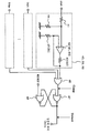
도 1은 본 발명이 적용되는 반도체 집적 회로의 구성예를 도시하는 도면.1 is a diagram showing a configuration example of a semiconductor integrated circuit to which the present invention is applied.
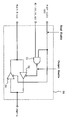
도 2는 부하 검지 회로, 기준 부하 출력부, 및 비교 회로의 구성예를 도시하는 도면.2 is a diagram illustrating an example of the configuration of a load detection circuit, a reference load output unit, and a comparison circuit.
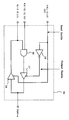
도 3은 입출력 버퍼의 구성예를 도시하는 도면.3 is a diagram illustrating a configuration example of an input / output buffer.
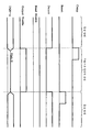
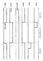
도 4는 동작 파형을 도시하는 도면.4 shows operation waveforms.
도 5는 입출력 버퍼의 구성예를 도시하는 도면.5 is a diagram illustrating a configuration example of an input / output buffer.
도 6은 본 발명이 적용되는 다른 반도체 집적 회로의 구성예를 도시하는 도면.6 is a diagram showing a configuration example of another semiconductor integrated circuit to which the present invention is applied.
도 7은 동작 파형을 도시하는 도면.7 illustrates an operational waveform.
<도면의 주요 부분에 대한 부호의 설명><Explanation of symbols for the main parts of the drawings>
1 : 반도체 집적 회로1: semiconductor integrated circuit
10 : 메모리 셀10: memory cell
30 : 입출력 버퍼30: I / O buffer
40 : 부하 검지 회로40: load detection circuit
42 : 콤퍼레이터42: comparator
43 : 출력 저항43: output resistance
45 : 제2 기준 저항45: second reference resistance
50 : 기준 부하 출력부50: reference load output
51 : 기준 레지스터51: reference register
60 : 비교 회로60: comparison circuit
61 : 디지털 비교 회로61: digital comparison circuit
70 : AD 변환 회로70: AD conversion circuit
Comp : 출력 신호Comp: output signal
Detect : 검출 신호Detect: Detection Signal
[특허 문헌 1] 일본특허공개 2002-73422호 공보[Patent Document 1] Japanese Patent Application Laid-Open No. 2002-73422
[특허 문헌 2] 일본특허공개 평9-16477호 공보[Patent Document 2] Japanese Patent Application Laid-Open No. 9-16477
[특허 문헌 3] 일본특허공개 2001-202167호 공보[Patent Document 3] Japanese Patent Application Laid-Open No. 2001-202167
[특허 문헌 4] 일본특허공개 평11-328036호 공보[Patent Document 4] Japanese Patent Application Laid-Open No. 11-328036
[특허 문헌 5] 일본특허공개 2001-195307호 공보[Patent Document 5] Japanese Patent Application Laid-Open No. 2001-195307
[특허 문헌 6] 일본특허공개 평10-320293호 공보[Patent Document 6] Japanese Patent Application Laid-Open No. 10-320293
[특허 문헌 7] 일본특허공개 평5-88986호 공보[Patent Document 7] Japanese Patent Application Laid-Open No. 5-88986
본 발명은 반도체 장치 및 반도체 장치에서의 제어 방법에 관한 것이다. 상세하게는, 해석 장치 등이 접속되어도 정보가 해석되지 않도록 한 반도체 장치 등에 관한 것이다.The present invention relates to a semiconductor device and a control method in the semiconductor device. Specifically, the present invention relates to a semiconductor device and the like in which information is not analyzed even when an analysis device or the like is connected.
최근, 노트형 퍼스널 컴퓨터나 PDA(Personal Digital Assistance) 등의 정보 단말 장치에서, 개인 정보나 기밀 정보의 누설이나 도난이 문제로 되고 있다. 이러한 정보는 통상적으로 정보 단말 장치의 메모리나 스토리지 디바이스에 보존된다. 따라서, 정보의 누설 등을 방지하기 위해서는 메모리 등에 대한 대책이 필요하게 된다.Background Art Recently, in information terminal devices such as notebook personal computers and PDAs (Personal Digital Assistance), leakage or theft of personal information or confidential information has become a problem. Such information is usually stored in a memory or a storage device of the information terminal apparatus. Therefore, in order to prevent leakage of information or the like, countermeasures for a memory or the like are necessary.
이러한 대책으로서, 예를 들면, 메모리의 제거를 검출하면 메모리 내의 데이터를 소거하도록 한 정보 처리 장치가 개시되어 있다(예를 들면, 특허 문헌 1).As such a countermeasure, for example, an information processing apparatus is disclosed that erases data in a memory when the removal of the memory is detected (for example, Patent Document 1).
또한, 기억 장치의 기밀성 데이터를 판독하기 위한 해독 키를 다른 기억 장치에 기억시키고, 기밀성 데이터를 기억한 기억 장치를 제거하면, 해독 키를 무효로 하게 하는 처리 장치가 개시되어 있다(예를 들면, 특허 문헌 2).Further, a processing apparatus is disclosed in which a decryption key for reading confidentiality data of a storage device is stored in another storage device and the decryption key is invalidated when the storage device storing the confidentiality data is removed (for example, Patent Document 2).
또한, 전원 오프 직전에 메모리의 내용을 암호화하여 메모리에 기입하고, 전원 온으로 복호화함으로써, 전원 오프 후에 메모리의 내용을 보고자 하여도 암호화되어 있기 때문에 볼 수 없도록 한 컴퓨터도 개시되어 있다(예를 들면, 특허 문헌 3).There is also disclosed a computer in which the contents of the memory are encrypted and written to the memory immediately before the power is turned off, and the contents of the memory are decrypted at power on so that the contents of the memory can not be viewed because the contents of the memory are encrypted even after the power is turned off. , Patent Document 3).
또한, 주위를 덮은 박막 전지를 제거하거나, 카드 자체를 개봉하거나 하면, 메모리의 내용을 소거하는 IC 카드(예를 들면, 특허 문헌 4∼6)나, 압전 재료에 응력을 가하면, 메모리의 내용을 리세트하는 안전 정보 외부 액세스 방지 기능을 갖 는 장치(예를 들면, 특허 문헌 7) 등도 있다.If the thin film battery covering the periphery is removed or the card itself is opened, the IC card (for example, Patent Documents 4 to 6) for erasing the contents of the memory or stress is applied to the piezoelectric material. There is also a device (for example, Patent Document 7) having a safety information reset function for preventing external access.
그러나, 이들 종래 기술은, 메모리를 장치 등으로부터 제거하면, 그 내용을 소거 등 함으로써 안전성을 확보하고 있는 것이 많고, 메모리 내용을 해석하는 로직 애널라이저나 오실로스코프 등의 계측 장치나 해석 장치를 사용하면, 메모리를 제거하지 않고 메모리 내용을 해석하는 것이 가능하게 된다.However, these prior arts often secure safety by removing the memory from a device or the like, and use a measuring device or analysis device such as a logic analyzer or an oscilloscope that analyzes the memory content. It is possible to interpret the memory contents without removing it.
또한, 전원 오프로 하고 암호화한다고 하여도, 전원 온 중에 이러한 해석 장치 등으로 메모리의 내용을 해석하는 것은 가능하다.Even when the power is turned off and encrypted, the contents of the memory can be analyzed by such an analysis device or the like during power on.
따라서, 이들 종래 기술에서는, 메모리에 개인 정보 등을 보존해 두면, 해석 장치 등에 의해서 그 내용이 해석되어 도난되는 문제가 있다.Therefore, in these prior arts, if personal information and the like are stored in the memory, the contents are analyzed and stolen by an analysis device or the like.
따라서, 본 발명은 상술한 문제점을 감안하여 이루어진 것으로, 그 목적은, 해석 장치나 계측 장치가 접속되어도 정보가 해석되지 않도록 한 반도체 장치 및 반도체 장치에서의 제어 방법을 제공하는 것에 있다.Accordingly, the present invention has been made in view of the above-described problems, and an object thereof is to provide a semiconductor device and a control method in the semiconductor device in which information is not analyzed even when an analysis device or a measurement device is connected.
상술한 목적을 달성하기 위해, 본 발명은, 단자에 접속된 부하의 부하량을 측정하고, 그 부하량이 기준 부하와 거의 일치할 때 제어 신호를 출력하는 부하 검지 수단과, 상기 제어 신호에 응답하여, 상기 단자로부터 데이터 출력을 정지하거나, 상기 단자에 특정한 논리를 출력하는 출력 제어 수단을 구비하는 반도체 장치인 것을 특징으로 한다.In order to achieve the above object, the present invention is a load detection means for measuring the load amount of the load connected to the terminal, and outputs a control signal when the load amount substantially matches the reference load, and in response to the control signal, A semiconductor device comprising output control means for stopping data output from the terminal or outputting specific logic to the terminal.
또한, 본 발명은, 상기 반도체 장치에서, 상기 부하 검지 수단에는, 상기 기 준 부하를 출력하는 기준 부하 출력 수단과, 측정된 상기 부하량과 상기 기준 부하 출력 수단으로부터의 상기 부하량을 비교하고, 그 비교 결과에 따라서 상기 제어 신호를 출력하는 비교 수단을 구비하는 것을 특징으로 한다.In the semiconductor device, the load detection means compares the reference load output means for outputting the reference load with the measured load amount and the load amount from the reference load output means. And a comparison means for outputting the control signal in accordance with the result.
또한, 본 발명은, 상기 반도체 장치에서, 상기 부하 검지 수단에는, 디지털화된 상기 기준 부하를 출력하는 기준 레지스터와, 측정된 상기 부하량을 디지털 변환하는 디지털 변환 수단과, 디지털 변환된 상기 부하량과 상기 기준 레지스터로부터의 상기 기준 부하를 비교하고, 그 비교 결과에 따라서 상기 제어 신호를 출력하는 비교 수단을 구비하는 것을 특징으로 한다.In the semiconductor device, the load detecting means includes: a reference register for outputting the digitized reference load, digital conversion means for digitally converting the measured load amount, the load amount and the reference value converted digitally. And comparison means for comparing the reference load from the register and outputting the control signal in accordance with the comparison result.
또한, 본 발명은, 상기 반도체 장치에서, 상기 기준 부하는, 상기 데이터를 판독하고 해석하는 해석 장치의 프로브가 상기 단자에 접속되었을 때의 부하량인 것을 특징으로 한다.The present invention is also characterized in that in the semiconductor device, the reference load is a load amount when a probe of an analysis device that reads and analyzes the data is connected to the terminal.
또한, 본 발명은, 상기 반도체 장치에서, 상기 데이터를 기억하는 기억 수단을 더 구비하고, 상기 출력 제어 수단은, 상기 제어 신호에 응답하여, 상기 기억 수단에 기억된 상기 데이터의 상기 단자로부터의 출력을 정지하거나, 특정한 논리를 출력하는 것을 특징으로 한다.The present invention further includes a storage means for storing the data in the semiconductor device, wherein the output control means outputs the data stored in the storage means from the terminal in response to the control signal. Stop or output specific logic.
또한, 상기 목적을 달성하기 위해, 본 발명은, 단자에 접속된 부하의 부하량을 측정하는 부하 검지 수단과, 상기 단자로부터 데이터를 출력하는 출력 제어 수단을 구비하는 반도체 장치에서의 제어 방법으로서, 측정된 상기 부하량이 기준 부하와 거의 일치할 때, 상기 부하 검지 수단으로부터 제어 신호를 출력하고, 상기 제어 신호에 응답하여, 상기 출력 제어 수단에 의해서 상기 단자로부터의 상기 데 이터의 출력을 정지하거나, 상기 출력 제어 수단으로부터 상기 단자에 특정한 논리를 출력하는 것을 특징으로 한다.Moreover, in order to achieve the said objective, this invention is a control method in a semiconductor device provided with the load detection means which measures the load quantity of the load connected to the terminal, and the output control means which outputs data from the said terminal, Comprising: When the loaded load amount almost matches the reference load, a control signal is output from the load detection means, and in response to the control signal, the output control means stops output of the data from the terminal, or A logic specific to the terminal is output from the output control means.
<실시예><Example>
이하, 도면을 참조하여 본 발명을 실시하기 위한 최량의 형태를 설명한다.EMBODIMENT OF THE INVENTION Hereinafter, the best form for implementing this invention with reference to drawings is demonstrated.
도 1은 본 발명에 따른 반도체 장치가 적용되는 반도체 집적 회로(1)의 구성예를 도시하는 도면이다.1 is a diagram showing an example of the configuration of a semiconductor integrated
도 1에 도시하는 바와 같이, 반도체 집적 회로(1)는, 메모리 셀(10)과, 커맨드 디코더(20)와, 입출력 버퍼(30)와, 부하 검지 회로(40)와, 기준 부하 출력부(50)와, 비교 회로(60)로 구성된다.As shown in FIG. 1, the semiconductor
메모리 셀(10)은 기억 소자로서, 여러 가지 데이터가 기억된다. 본 실시예에서는, 기밀 정보나 개인 정보 등의 데이터도 기억된다.The
커맨드 디코더(20)는 입출력 버퍼(30)와 접속되고, 메모리 셀(10)에의 데이터의 기입과 판독을 나타내는 인에이블 신호(각각 「WriteEnable」, 「ReadEnable」)를 출력한다.The
입출력 버퍼(30)는 메모리 셀(10) 및 단자 DQ에도 접속된다. 입출력 버퍼(30)는 단자 DQ로부터 입력된 데이터를 일시 기억하고, 그 후 메모리 셀(10)에 출력한다. 또한, 메모리 셀(10)로부터 판독된 데이터도 일시 기억하고, 그 후 단자 DQ에 출력한다. 이러한 동작들은 인에이블 신호(각각 「WriteEnable」, 「ReadEnable」)에 기초하여 행해진다.The input /
부하 검지 회로(40)은 단자 DQ에 접속된다. 부하 검지 회로(40)는 단자 DQ 에 접속된 부하부(100)의 부하값(예를 들면, 부하 전류나 부하 용량 등)을 검지하고, 그 값을 출력한다. 또한, 부하부(100)는, 예를 들면 컨트롤러용 IC나, 해석 장치의 프로브 등이다.The
기준 부하 출력부(50)는 기준 부하를 출력한다. 기준 부하란, 부하부(100)의 부하값과 해석 장치의 프로브(탐침)의 부하의 합을 수치화한 값이다.The reference
비교 회로(60)는 부하 검지 회로(40)와 기준 부하 출력부(50)에 접속됨과 함께, 입출력 버퍼(30)에도 접속된다. 비교 회로(60)는 부하 검지 회로(40)로부터의 부하와 기준 부하 출력부(50)로부터의 기준 부하를 비교하고, 양자가 일치하였을 때에 제어 신호를 입출력 버퍼(30)에 출력한다. 즉, 단자 DQ에 프로브가 접속되면, 비교 회로(60)로부터 제어 신호가 출력된다.The
입출력 버퍼(30)는, 이 제어 신호에 의해, 메모리 셀(10)로부터 판독된 데이터의 출력을 정지하거나, 특정한 고정화된 논리(「1」 또는 「0」)를 단자 DQ에 출력한다. 즉, 단자 DQ에 프로브가 접속되면, 단자 DQ로부터 데이터 출력이 정지되거나, 특정한 논리가 출력되어, 메모리 셀(10)에 기억된 데이터가 판독되지 않도록 하고 있다.The input /
도 2는 부하 검지 회로(40)와 기준 부하 출력부(50) 및 비교 회로(60)를 포함하는 회로의 상세한 구성예를 도시하는 도면이다. 이들 회로(40, 50, 60)는 단자 DQ의 개수분(도 2의 예에서는 n+1개) 설치되어 있다.FIG. 2 is a diagram showing a detailed configuration example of a circuit including the
회로(40, 50, 60)는, 입력 저항(41)과, 콤퍼레이터(42)와, 출력 저항(43)과, 제1 기준 저항(44)과, 제2 기준 저항(45)으로 구성된다.The
입력 저항(41)의 일단은 단자 DQ0에, 타단은 콤퍼레이터(42)에 접속된다. 또한, 입력 저항(41)과 콤퍼레이터(42) 사이에, 타단이 접지된 제1 기준 저항(44)의 일단이 접속된다.One end of the
또한, 콤퍼레이터(42)의 출력측에 출력 저항(43)이 설치되고, 그 출력 저항(43)의 출력이 콤퍼레이터(42)에도 입력되도록 설치된다. 그리고, 타단이 접지된 제2 기준 저항(45)의 일단이, 출력 저항(43)의 출력과 콤퍼레이터(42)의 입력 사이에 접속된다.In addition, an
콤퍼레이터(42)는, 플러스(+)측을 기준 전압으로 하고, 마이너스(-)측에의 전압값이 기준 전압보다 높으면, 단자 DQ0에 입력된 입력 전류를 출력한다.The comparator 42 uses the positive side as a reference voltage, and outputs an input current input to the terminal DQ0 when the voltage value on the negative side is higher than the reference voltage.
한편, 단자 DQ에 프로브가 접속되었을 때와, 컨트롤러용 IC 등이 접속되었을 때(통상 상태일 때)에서, 단자 DQ0에 입력되는 전류는 서로 다른 값으로 된다. 따라서, 단자 DQ에 프로브가 접속되었을 때에 그 전류를 출력하도록 기준 전압을 조정하면, 회로(40, 50, 60)로부터는 그 때에만 일정 전압값이 출력되게 된다. 예를 들면, 프로브가 접속되면, 회로(40, 50, 60)는 논리 「HIGH」에 대응하는 전압값을 출력하고, 그 이외에는 「LOW」에 대응하는 전압값을 출력한다.On the other hand, when the probe is connected to the terminal DQ and when the controller IC or the like is connected (in the normal state), the current input to the terminal DQ0 is different from each other. Therefore, when the reference voltage is adjusted to output the current when the probe is connected to the terminal DQ, the
또한, 콤퍼레이터(42)의 기준 전압은 출력 저항(43)과 제2 기준 저항(45)의 저항값을 변경함으로써 조정된다. 예를 들면, 외부 단자가 저항(43, 45)과 접속되어 외부로부터의 제어 신호에 의해 저항값을 변경함으로써 기준 전압을 조정할 수 있다. 마찬가지로 하여, 제1 기준 전압(44)도 외부로부터 조정 가능하다.In addition, the reference voltage of the comparator 42 is adjusted by changing the resistance values of the
또한, 콤퍼레이터(42)의 플러스측의 기준 전압이 기준 부하로 되어 마이너스 측의 전압값과 비교되고 있기 때문에, 콤퍼레이터(42)가 부하 검지 회로(40) 및 비교 회로(60)에 해당하고, 출력 저항(43)과 제2 기준 저항(45)이 기준 부하 출력부(50)에 해당한다.In addition, since the reference voltage on the positive side of the comparator 42 becomes the reference load and is compared with the voltage value on the negative side, the comparator 42 corresponds to the
각 회로(40, 50, 60)의 후단에는, OR 회로(46), 2개의 NOR 회로(47, 48)로 구성되는 래치 회로가 설치되어 있다.At the rear end of each of the
OR 회로(46)는 단자 DQ0∼DQn에 프로브가 접속되었는지의 여부를 나타내는 신호 Comp를 출력하고, 그 출력이 래치 회로에서 래치되어, 검출 신호 Detect가 출력된다.The OR
예를 들면, 어느 한 단자 DQ0∼DQn에 프로브가 접속되면, 신호 Comp가 「High」로 되고, 검출 신호 Detect가 「Low」로 된다. 이 출력 신호 Comp 또는 검출 신호 Detect가, 비교 회로(60)로부터 입출력 버퍼(30)에 출력되는 제어 신호에 대응한다.For example, when a probe is connected to either of the terminals DQ0 to DQn, the signal Comp becomes "High" and the detection signal Detect becomes "Low". This output signal Comp or detection signal Detect corresponds to the control signal output from the
도 3은 입출력 버퍼(30)의 구성예를 도시하는 도면이다. 메모리 셀(10)로부터 판독된 데이터의 출력을 정지하는 경우의 구성도를 도시한다.3 is a diagram illustrating a configuration example of the input /
입출력 버퍼(30)는, NAND 회로(31)와, 제1 및 제2 버퍼 회로(32, 33)로 구성된다.The input /
NAND 회로(31)는 커맨드 디코더(20)와 NOR 회로(47)(도 2 참조)에 접속되어, 커맨드 디코더(20)로부터의 Enable 신호와 비교 회로(60)로부터의 출력 신호가 입력되고, 출력 신호 OutputEnable을 출력한다.The
제1 버퍼(32)는 메모리 셀(10)로부터의 출력을 기억하고, 단자 DQ0∼DQn에 출력한다. 이 제1 버퍼(32)는 메모리 셀(10)로부터의 데이터의 판독에 대응하는 버퍼이다.The
또한, 제1 버퍼(32)는 3 스테이트 회로 구성으로 되어 있어, 「HIGH」, 「LOW」 외에, 하이 임피던스 상태(이하, 「High-Z」)를 취할 수 있다. 「HIGH-Z」를 취할 수 있는지의 여부는 출력 신호 OutputEnable에 기초한다.In addition, the
예를 들면, 출력 신호 OutputEnable이 「HIGH」일 때, 「High-Z」 상태로 되어, 제1 버퍼(32)는 전기적인 접속이 해제된 상태로 되어 단자 DQ0∼DQn에의 출력이 정지된다. 한편, 출력 신호 OutputEnable이 「LOW」일 때, 입력에 따른 논리가 출력된다.For example, when the output signal OutputEnable is "HIGH", the output signal is "High-Z", the
제2 버퍼(33)도 마찬가지로 커맨드 디코더(20)로부터의 신호에 기초하여 「HIGH-Z」, 「LOW」, 「HIGH」의 3 가지 상태를 취할 수 있다. 제2 버퍼(33)는 메모리 셀(10)에의 기입에 대응한 버퍼이다.Similarly, the
도 4는 도 2 및 도 3에 도시하는 구성에서의 각 신호의 동작 파형도이다. 통상 상태에서 프로브가 단자 DQ에 접속되고, 그 후 다시 통상 상태로 되돌아간 경우의 예이다.4 is an operation waveform diagram of each signal in the configuration shown in FIGS. 2 and 3. This is an example of the case where the probe is connected to the terminal DQ in the normal state and then returned to the normal state again.
우선, 통상 상태에서는, 각 회로(40, 50, 60)로부터 「LOW」가 출력된다. 따라서, OR 회로(46)의 출력 신호 Comp는 「LOW」로 된다. 그리고, 2개의 NOT 회로(47, 48)로 구성되는 래치 회로에서 반전되어, 검출 신호 Detect는 「HIGH」로 된다.First, in the normal state, "LOW" is output from each of the
한편, 커맨드 디코더(20)로부터, 메모리 셀(10)로부터의 판독을 나타내는 ReadEnable 신호가 출력되고 있을 때(ReadEnable이 「HIGH」일 때), NAND 회로(31)의 출력 신호 OutputEnable은 함께 입력이 「HIGH」이기 때문에, 「LOW」가 출력된다. 이에 의해, 제1 버퍼 회로(32)는 메모리 셀(10)로부터 단자 DQ0∼DQn에 데이터를 출력한다.On the other hand, when the ReadEnable signal indicating the read from the
이러한 상태에서, 예를 들면 단자 DQ0에 프로브가 접속되었을 때, 회로(40, 50, 60)로부터는 프로브가 접속된 것을 나타내는 신호를 출력하기 때문에, 출력 신호 Comp는 「HIGH」로 된다. 그리고, 검출 신호 Detect는 「LOW」로 된다.In such a state, for example, when a probe is connected to the terminal DQ0, a signal indicating that the probe is connected is output from the
커맨드 디코더(20)로부터 ReadEnable 신호가 「HIGH」로 출력되고 있는 상태에서, 검출 신호 「LOW」가 NAND 회로(31)에 입력됨으로써, 그 출력 신호 OutputEnable은 「HIGH」로 된다. 따라서, 제1 버퍼 회로(32)는 「HIGH-Z」를 출력하고, 메모리 셀(10)로부터의 판독이 정지된다. 즉, 단자 DQ0에 프로브가 접속되면, 메모리(10)로부터의 판독이 정지된다.The detection signal "LOW" is input to the
그 후, 프로브가 단자 DQ0로부터 떨어짐으로써 통상 상태로 되돌아가서, 출력 신호 Comp는 「LOW」로 된다. 이 경우에, 도 2에 도시하는 NOR 회로(48)의 입력단으로부터 RESET 신호가 입력되어(「HIGH」), 각 회로가 통상 상태로 복귀되게 된다. 이후에는 상술한 통상 상태와 마찬가지로 동작한다.Thereafter, the probe returns from the terminal DQ0 to the normal state, and the output signal Comp becomes "LOW". In this case, the RESET signal is input ("HIGH") from the input terminal of the NOR
도 5는 도 4와 마찬가지로 입출력 버퍼(30)의 구성예를 도시하는 도면인데, 고정된 논리를 계속해서 출력하도록 한 경우의 예이다.FIG. 5 is a diagram showing an example of the configuration of the input /
입출력 버퍼(30)는, NOT 회로(35)와, AND 회로(36)와, 제1 및 제2 버퍼 회로(37, 38)로 구성된다.The input /
NOT 회로(35)는 커맨드 디코더(20)에 접속되어 커맨드 디코더(20)로부터의 Enable 신호가 입력되고, OutputEnable 신호를 출력한다.The
AND 회로(36)는 메모리 셀(10)과 NOR 회로(47)(도 2 참조)에 접속되고, 비교 회로(60)로부터의 출력 신호에 따라 논리를 결정한다.The AND
제1 버퍼(37)는 AND 회로(36)로부터의 출력을 기억하고, 단자 DQ0∼DQn에 출력한다. 이 제1 버퍼(37)는 메모리 셀(10)로부터의 데이터의 판독에 대응하는 버퍼이다.The
또한, 제1 버퍼(37)는 3 스테이트 회로 구성으로 되어 있고, 「HIGH」, 「LOW」 외에, 하이 임피던스 상태(이하, 「High-Z」)를 취할 수 있다. 「High-Z」를 취할 수 있는지의 여부는, 출력 신호 OutputEnable에 기초한다.In addition, the
예를 들면, 출력 신호 OutputEnable이 「HIGH」일 때, 「High-Z」 상태로 되어, 제1 버퍼(37)는 전기적인 접속이 해제된 상태로 되어 단자 DQ0∼DQn에의 출력이 정지된다. 한편, 출력 신호 OutputEnable이 「LOW」일 때, 입력에 따른 논리가 출력된다.For example, when the output signal OutputEnable is "HIGH", the output signal is "High-Z", the
제2 버퍼(38)도 마찬가지로 커맨드 디코더(20)로부터의 신호에 기초하여 「High-Z」, 「LOW」, 「HIGH」의 3 가지 상태를 취할 수 있다. 제2 버퍼(38)는 메모리 셀(10)에의 기입에 대응한 버퍼이다.Similarly, the
도 7은 도 2 및 도 5에 도시하는 구성에서의 각 신호의 동작 파형도이다. 통상 상태에서 프로브가 단자 DQ에 접속되고, 그 후 다시 통상 상태로 되돌아간 경우의 예이다.7 is an operation waveform diagram of each signal in the configuration shown in FIGS. 2 and 5. This is an example of the case where the probe is connected to the terminal DQ in the normal state and then returned to the normal state again.
우선, 통상 상태에서는, 각 회로(40, 50, 60)로부터 「LOW」가 출력된다. 따라서, OR 회로(46)의 출력 신호 Comp는 「LOW」로 된다. 그리고, 2개의 NOR 회로(47, 48)로 구성되는 래치 회로에서 반전되어, 검출 신호 Detect는 「HIGH」로 된다.First, in the normal state, "LOW" is output from each of the
한편, 커맨드 디코더(20)로부터, 메모리 셀(10)로부터의 판독을 나타내는 ReadEnable 신호가 출력되고 있을 때(ReadEnable이 「HIGH」일 때), NOT 회로(35)로부터는 「LOW」가 출력된다. 이에 의해, 제1 버퍼 회로(37)는 메모리 셀(10)로부터 단자 DQ0∼DQn에 데이터가 출력된다.On the other hand, when the ReadEnable signal indicating the read from the
이러한 상태에서, 예를 들면 단자 DQ0에 프로브가 접속되었을 때, 회로(40, 50, 60)로부터는 프로브가 접속된 것을 나타내는 신호를 출력하기 때문에, 출력 신호 Comp는 「HIGH」로 된다. 그리고, 검출 신호 Detect는 「LOW」로 된다.In such a state, for example, when a probe is connected to the terminal DQ0, a signal indicating that the probe is connected is output from the
커맨드 디코더(20)로부터 ReadEnable 신호가 「HIGH」로 출력되고 있는 상태에서, 검출 신호 「LOW」가 AND 회로(36)에 입력됨으로써, 그 출력 신호는 메모리 셀(10)의 논리에 상관없이 「LOW」로 된다. 따라서, 제1 버퍼 회로(37)는 「LOW」를 출력하고, 메모리 셀(10)로부터의 판독이 「LOW」에 고정된다. 즉, 단자 DQ0에 프로브가 접속되면, 메모리(10)로부터의 판독은 항상 「LOW」를 유지한다.When the ReadEnable signal is output from the
그 후, 프로브가 단자 DQ0로부터 떨어짐으로써 통상 상태로 되돌아가서, 출력 신호 Comp는 「LOW」로 된다. 이 경우에, 도 2에 도시하는 NOR 회로(48)의 입력단으로부터 RESET 신호가 입력되어(「HIGH」), 각 회로가 통상 상태로 복귀되게 된다. 이후는 상술한 통상 상태와 마찬가지로 동작한다.Thereafter, the probe returns from the terminal DQ0 to the normal state, and the output signal Comp becomes "LOW". In this case, the RESET signal is input ("HIGH") from the input terminal of the NOR
도 1에 도시하는 예에서는, 아날로그값을 검출하여 비교하도록 하였지만, 예를 들면, 도 6에 도시하는 구성이어도 본 발명은 적용 가능하다. 이 경우, 부하 검지 회로(40)에 의해 검지된 부하값을 AD 변환 회로(70)에 의해 디지털값으로 변환해서, 디지털 비교 회로(61)에 출력한다.In the example shown in FIG. 1, analog values are detected and compared. For example, the present invention can be applied even in the configuration shown in FIG. In this case, the load value detected by the
프로브가 단자 DQ에 접속되었을 때의 부하를 나타내는 디지털값을 기준 레지스터(51)로부터 출력하고, 디지털 비교 회로(61)는 이 기준값과 AD 변환 회로(70)로부터의 디지털값을 비교하고, 일치하였을 때에 제어 신호를 출력한다.The digital value indicating the load when the probe is connected to the terminal DQ is output from the
입출력 버퍼(30)에서는, 도 1에 도시하는 경우와 마찬가지로, 이 제어 신호가 입력되었을 때에, 메모리 셀(10)로부터의 출력을 정지하거나, 고정화된 특정한 논리를 계속해서 출력함으로써, 메모리(10)에 기억된 데이터를 판독하지 못하게 한다. 따라서, 프로브가 접속되었을 때에 단자 DQ로부터 해석 장치로 데이터가 출력되지 않기 때문에, 데이터는 해석되지 않는다.In the input /
또한, 도 2에 도시하는 회로는 일례이고, 프로브가 접속되었는지의 여부를 나타내는 출력 신호 Comp나 검출 신호 Detct가 출력될 수 있는 것이면 어떠한 회로 구성이어도 된다. 예를 들면, OR 회로(46)를 AND 회로로 한다거나, 래치 회로(NOR 회로(47, 48))를 삭제하여도 된다.In addition, the circuit shown in FIG. 2 is an example, and what kind of circuit structure may be sufficient as long as the output signal Comp which shows whether the probe is connected, or the detection signal Detct can be output. For example, the
또한, 도 3이나 도 5에 도시하는 회로도, 메모리 셀(10)로부터의 출력을 정지하거나, 특정한 논리를 계속해서 출력하는 회로 구성이면 어떠한 것이어도 된다. 예를 들면, NAND 회로(31)를 AND 회로로 하여도 된다. 어느 경우에도, 상술한 예와 마찬가지의 작용 효과를 발휘한다.The circuit shown in FIG. 3 or FIG. 5 may be any circuit structure as long as the output from the
또한, 상술한 예에서는, 반도체 집적 회로(1) 내에 메모리 셀(10)이 설치되어 있는 예로 설명하였지만, 예를 들면, 메모리 셀(10)이 반도체 집적 회로(1)의 외부에 설치되어 있는 경우에도 본 발명은 적용 가능하다. 이 경우에도, 상술한 예와 마찬가지의 작용 효과를 발휘한다.In the above-described example, the
또한, 도 1이나 도 5에 도시하는 반도체 집적 회로(1)는, 노트형 퍼스널 컴퓨터나, PDA, 휴대 전화 등의 정보 휴대 단말기에 사용하는 것이 가능하고, 이 경우에도, 상술한 예와 마찬가지의 작용 효과를 발휘한다.In addition, the semiconductor integrated
이상, 정리하면, 부기와 같이 된다.In summary, it is like bookkeeping.
(부기 1)(Book 1)
단자에 접속된 부하의 부하량을 측정하고, 그 부하량이 기준 부하와 거의 일치할 때, 제어 신호를 출력하는 부하 검지 수단과,Load detection means for measuring a load amount of the load connected to the terminal and outputting a control signal when the load amount substantially matches the reference load;
상기 제어 신호에 응답하여, 상기 단자로부터 데이터 출력을 정지하거나, 상기 단자에 특정한 논리를 출력하는 출력 제어 수단Output control means for stopping data output from the terminal or outputting logic specific to the terminal in response to the control signal
을 구비하는 것을 특징하는 반도체 장치.And a semiconductor device.
(부기 2)(Supplementary Note 2)
부기 1에 기재된 반도체 장치에서,In the semiconductor device according to
상기 부하 검지 수단에는,In the load detection means,
상기 기준 부하를 출력하는 기준 부하 출력 수단과,Reference load output means for outputting the reference load;
측정된 상기 부하량과 상기 기준 부하 출력 수단으로부터의 상기 부하량을 비교하고, 그 비교 결과에 따라서 상기 제어 신호를 출력하는 비교 수단Comparison means for comparing the measured load amount with the load amount from the reference load output means and outputting the control signal in accordance with the comparison result
을 구비하는 것을 특징으로 하는 반도체 장치.A semiconductor device comprising: a.
(부기 3)(Supplementary Note 3)
부기 1에 기재된 반도체 장치에서,In the semiconductor device according to
상기 부하 검지 수단에는,In the load detection means,
디지털화된 상기 기준 부하를 출력하는 기준 레지스터와,A reference register for outputting the digitized reference load;
측정된 상기 부하량을 디지털 변환하는 디지털 변환 수단과,Digital conversion means for digitally converting the measured load;
디지털 변환된 상기 부하량과 상기 기준 레지스터로부터의 상기 기준 부하를 비교하고, 그 비교 결과에 따라서 상기 제어 신호를 출력하는 비교 수단Comparison means for comparing the digitally converted load amount with the reference load from the reference register and outputting the control signal in accordance with the comparison result
을 구비하는 것을 특징으로 하는 반도체 장치.A semiconductor device comprising: a.
(부기 4)(Appendix 4)
부기 1에 기재된 반도체 장치에서,In the semiconductor device according to
상기 기준 부하는, 상기 데이터를 판독하고 해석하는 해석 장치의 프로브가 상기 단자에 접속되었을 때의 부하량인 것을 특징으로 하는 반도체 장치.And the reference load is a load amount when a probe of an analyzer for reading and analyzing the data is connected to the terminal.
(부기 5)(Appendix 5)
부기 1에 기재된 반도체 장치에서,In the semiconductor device according to
상기 데이터를 기억하는 기억 수단Storage means for storing the data
을 더 구비하고,Further provided,
상기 출력 제어 수단은, 상기 제어 신호에 응답하여, 상기 기억 수단에 기억된 상기 데이터의 상기 단자로부터의 출력을 정지하거나, 특정한 논리를 출력하는 것을 특징으로 하는 반도체 장치.And the output control means stops the output from the terminal of the data stored in the storage means or outputs a specific logic in response to the control signal.
(부기 6)(Supplementary Note 6)
단자에 접속된 부하의 부하량을 측정하는 부하 검지 수단과, 상기 단자로부터 데이터를 출력하는 출력 제어 수단을 구비하는 반도체 장치에서의 제어 방법으로서,A control method in a semiconductor device comprising load detection means for measuring a load amount of a load connected to a terminal and an output control means for outputting data from the terminal,
측정된 상기 부하량이 기준 부하와 거의 일치할 때, 상기 부하 검지 수단으로부터 제어 신호를 출력하고,Outputting a control signal from the load detecting means when the measured load amount substantially matches the reference load,
상기 제어 신호에 응답하여, 상기 출력 제어 수단에 의해서 상기 단자로부터의 상기 데이터의 출력을 정지하거나, 상기 출력 제어 수단으로부터 상기 단자에 특정한 논리를 출력하는 것을 특징으로 하는 제어 방법.In response to the control signal, outputting the data from the terminal by the output control means, or outputting logic specific to the terminal from the output control means.
본 발명에 따르면, 계측 장치나 해석 장치가 접속되어도 정보가 해석되지 않도록 한 반도체 장치 및 반도체 장치에서의 제어 방법을 제공할 수 있다.According to the present invention, it is possible to provide a semiconductor device and a control method in the semiconductor device in which information is not analyzed even when a measurement device or an analysis device is connected.
Claims (5)
Applications Claiming Priority (2)
| Application Number | Priority Date | Filing Date | Title |
|---|---|---|---|
| JPJP-P-2005-00238617 | 2005-08-19 | ||
| JP2005238617A JP4754903B2 (en) | 2005-08-19 | 2005-08-19 | Semiconductor device and control method in semiconductor device |
Publications (1)
| Publication Number | Publication Date |
|---|---|
| KR100683096B1 true KR100683096B1 (en) | 2007-02-16 |
Family
ID=37766567
Family Applications (1)
| Application Number | Title | Priority Date | Filing Date |
|---|---|---|---|
| KR1020050124571A Expired - Fee Related KR100683096B1 (en) | 2005-08-19 | 2005-12-16 | Semiconductor device and control method in semiconductor device |
Country Status (3)
| Country | Link |
|---|---|
| US (1) | US7614565B2 (en) |
| JP (1) | JP4754903B2 (en) |
| KR (1) | KR100683096B1 (en) |
Families Citing this family (3)
| Publication number | Priority date | Publication date | Assignee | Title |
|---|---|---|---|---|
| GB0223327D0 (en) * | 2002-10-08 | 2002-11-13 | Ranier Ltd | Artificial spinal disc |
| KR101075495B1 (en) * | 2010-07-06 | 2011-10-21 | 주식회사 하이닉스반도체 | Circuit for selecting a plurality of semiconductor devices included in the semiconductor module and its operation method |
| JP6358497B2 (en) * | 2014-04-19 | 2018-07-18 | Tianma Japan株式会社 | Control device |
Citations (4)
| Publication number | Priority date | Publication date | Assignee | Title |
|---|---|---|---|---|
| JP2811142B2 (en) * | 1992-04-30 | 1998-10-15 | アツデン株式会社 | Power management system |
| KR20030026551A (en) * | 2001-09-26 | 2003-04-03 | 삼성전자주식회사 | A memory module having the function of compensating output driving circuits of memory chips |
| JP2005027420A (en) | 2003-07-02 | 2005-01-27 | Fuji Electric Fa Components & Systems Co Ltd | Electric motor drive control device |
| KR20050022625A (en) * | 2003-08-29 | 2005-03-08 | 삼성전자주식회사 | Method for protecting data in data storage system and disc drive using the same |
Family Cites Families (14)
| Publication number | Priority date | Publication date | Assignee | Title |
|---|---|---|---|---|
| JPS63208145A (en) * | 1987-02-25 | 1988-08-29 | Hitachi Ltd | IC card |
| EP0509567A3 (en) | 1991-03-28 | 1993-04-07 | N.V. Philips' Gloeilampenfabrieken | Device with protection against access to secure information |
| JP3654938B2 (en) * | 1994-09-20 | 2005-06-02 | 大日本印刷株式会社 | Telephone |
| JP3479390B2 (en) | 1995-06-30 | 2003-12-15 | 沖電気工業株式会社 | Decryption prevention method and information processing device for confidentiality data |
| JP4212068B2 (en) | 1997-05-19 | 2009-01-21 | ローム株式会社 | IC card and IC chip module |
| JPH11120309A (en) * | 1997-10-15 | 1999-04-30 | Hitachi Ltd | Communication device with tamper-resistant function |
| JP3641135B2 (en) | 1998-05-20 | 2005-04-20 | 日本電信電話株式会社 | IC card |
| JP2000347848A (en) * | 1999-03-30 | 2000-12-15 | Sony Corp | Semiconductor IC, information processing method, information processing apparatus, and program storage medium |
| JP2001195307A (en) | 2000-01-06 | 2001-07-19 | Nippon Telegr & Teleph Corp <Ntt> | Semiconductor device |
| JP2001202167A (en) | 2000-01-20 | 2001-07-27 | Toyo Commun Equip Co Ltd | Computer and control method thereof |
| JP2002073422A (en) | 2000-09-05 | 2002-03-12 | Sharp Corp | Information processing device |
| JP3983521B2 (en) * | 2001-11-14 | 2007-09-26 | シャープ株式会社 | Semiconductor device and IC card |
| DE60310139T2 (en) * | 2003-01-14 | 2007-09-27 | Koninklijke Philips Electronics N.V. | DETECTION OF MANIPULATION ON A CHIP CARD INTERFACE |
| JP4103753B2 (en) * | 2003-09-19 | 2008-06-18 | 日産自動車株式会社 | Engine exhaust purification system |
-
2005
- 2005-08-19 JP JP2005238617A patent/JP4754903B2/en not_active Expired - Fee Related
- 2005-11-28 US US11/287,231 patent/US7614565B2/en not_active Expired - Fee Related
- 2005-12-16 KR KR1020050124571A patent/KR100683096B1/en not_active Expired - Fee Related
Patent Citations (4)
| Publication number | Priority date | Publication date | Assignee | Title |
|---|---|---|---|---|
| JP2811142B2 (en) * | 1992-04-30 | 1998-10-15 | アツデン株式会社 | Power management system |
| KR20030026551A (en) * | 2001-09-26 | 2003-04-03 | 삼성전자주식회사 | A memory module having the function of compensating output driving circuits of memory chips |
| JP2005027420A (en) | 2003-07-02 | 2005-01-27 | Fuji Electric Fa Components & Systems Co Ltd | Electric motor drive control device |
| KR20050022625A (en) * | 2003-08-29 | 2005-03-08 | 삼성전자주식회사 | Method for protecting data in data storage system and disc drive using the same |
Also Published As
| Publication number | Publication date |
|---|---|
| US7614565B2 (en) | 2009-11-10 |
| JP4754903B2 (en) | 2011-08-24 |
| US20070040038A1 (en) | 2007-02-22 |
| JP2007052709A (en) | 2007-03-01 |
Similar Documents
| Publication | Publication Date | Title |
|---|---|---|
| US7837110B1 (en) | Magnetic stripe reader having digital peak detector | |
| US6059191A (en) | Chip card | |
| US20110202709A1 (en) | Optimizing storage of common patterns in flash memory | |
| US8316242B2 (en) | Cryptoprocessor with improved data protection | |
| US8627116B2 (en) | Power conservation in an intrusion detection system | |
| KR100296199B1 (en) | Memory card | |
| US6499092B1 (en) | Method and apparatus for performing access censorship in a data processing system | |
| US7551098B1 (en) | Point of sale terminal having pulsed current tamper control sensing | |
| KR100683096B1 (en) | Semiconductor device and control method in semiconductor device | |
| KR970076884A (en) | Multi-bit test circuit of semiconductor memory device and test method thereof | |
| US7420866B2 (en) | Method and system of operating mode detection | |
| US7183792B2 (en) | Method and system for detecting a mode of operation of an integrated circuit, and a memory device including same | |
| US20050157565A1 (en) | Semiconductor device for detecting memory failure and method thereof | |
| US8495443B1 (en) | Secure register scan bypass | |
| US20070282568A1 (en) | Sensor control circuit | |
| US11327882B2 (en) | Method and apparatus for eliminating bit disturbance errors in non-volatile memory devices | |
| US8589749B1 (en) | Memory content protection during scan dumps and memory dumps | |
| CN1251183A (en) | Integrated circuit and method for testing the same | |
| JP2009036782A (en) | How to determine drop and collision of portable device | |
| JP4202116B2 (en) | Memory control circuit, memory device and microcomputer | |
| CN101770810B (en) | Semiconductor apparatus having a plurality of action modes | |
| US20070247182A1 (en) | Protection of security key information | |
| KR100222576B1 (en) | IC card circuit and its test method | |
| US7340313B2 (en) | Monitoring device for monitoring internal signals during initialization of an electronic circuit | |
| JP2006172384A (en) | Semiconductor device |
Legal Events
| Date | Code | Title | Description |
|---|---|---|---|
| A201 | Request for examination | ||
| PA0109 | Patent application |
St.27 status event code: A-0-1-A10-A12-nap-PA0109 |
|
| PA0201 | Request for examination |
St.27 status event code: A-1-2-D10-D11-exm-PA0201 |
|
| D13-X000 | Search requested |
St.27 status event code: A-1-2-D10-D13-srh-X000 |
|
| D14-X000 | Search report completed |
St.27 status event code: A-1-2-D10-D14-srh-X000 |
|
| E701 | Decision to grant or registration of patent right | ||
| PE0701 | Decision of registration |
St.27 status event code: A-1-2-D10-D22-exm-PE0701 |
|
| GRNT | Written decision to grant | ||
| PR0701 | Registration of establishment |
St.27 status event code: A-2-4-F10-F11-exm-PR0701 |
|
| PR1002 | Payment of registration fee |
St.27 status event code: A-2-2-U10-U11-oth-PR1002 Fee payment year number: 1 |
|
| PG1601 | Publication of registration |
St.27 status event code: A-4-4-Q10-Q13-nap-PG1601 |
|
| R17-X000 | Change to representative recorded |
St.27 status event code: A-5-5-R10-R17-oth-X000 |
|
| PR1001 | Payment of annual fee |
St.27 status event code: A-4-4-U10-U11-oth-PR1001 Fee payment year number: 4 |
|
| PR1001 | Payment of annual fee |
St.27 status event code: A-4-4-U10-U11-oth-PR1001 Fee payment year number: 5 |
|
| PR1001 | Payment of annual fee |
St.27 status event code: A-4-4-U10-U11-oth-PR1001 Fee payment year number: 6 |
|
| FPAY | Annual fee payment |
Payment date: 20130118 Year of fee payment: 7 |
|
| PR1001 | Payment of annual fee |
St.27 status event code: A-4-4-U10-U11-oth-PR1001 Fee payment year number: 7 |
|
| FPAY | Annual fee payment |
Payment date: 20140117 Year of fee payment: 8 |
|
| PR1001 | Payment of annual fee |
St.27 status event code: A-4-4-U10-U11-oth-PR1001 Fee payment year number: 8 |
|
| FPAY | Annual fee payment |
Payment date: 20150119 Year of fee payment: 9 |
|
| PR1001 | Payment of annual fee |
St.27 status event code: A-4-4-U10-U11-oth-PR1001 Fee payment year number: 9 |
|
| FPAY | Annual fee payment |
Payment date: 20160119 Year of fee payment: 10 |
|
| PR1001 | Payment of annual fee |
St.27 status event code: A-4-4-U10-U11-oth-PR1001 Fee payment year number: 10 |
|
| FPAY | Annual fee payment |
Payment date: 20170119 Year of fee payment: 11 |
|
| PR1001 | Payment of annual fee |
St.27 status event code: A-4-4-U10-U11-oth-PR1001 Fee payment year number: 11 |
|
| LAPS | Lapse due to unpaid annual fee | ||
| PC1903 | Unpaid annual fee |
St.27 status event code: A-4-4-U10-U13-oth-PC1903 Not in force date: 20180209 Payment event data comment text: Termination Category : DEFAULT_OF_REGISTRATION_FEE |
|
| PC1903 | Unpaid annual fee |
St.27 status event code: N-4-6-H10-H13-oth-PC1903 Ip right cessation event data comment text: Termination Category : DEFAULT_OF_REGISTRATION_FEE Not in force date: 20180209 |