KR100683096B1 - 반도체 장치 및 반도체 장치에서의 제어 방법 - Google Patents
반도체 장치 및 반도체 장치에서의 제어 방법 Download PDFInfo
- Publication number
- KR100683096B1 KR100683096B1 KR1020050124571A KR20050124571A KR100683096B1 KR 100683096 B1 KR100683096 B1 KR 100683096B1 KR 1020050124571 A KR1020050124571 A KR 1020050124571A KR 20050124571 A KR20050124571 A KR 20050124571A KR 100683096 B1 KR100683096 B1 KR 100683096B1
- Authority
- KR
- South Korea
- Prior art keywords
- load
- output
- terminal
- semiconductor device
- outputting
- Prior art date
- Legal status (The legal status is an assumption and is not a legal conclusion. Google has not performed a legal analysis and makes no representation as to the accuracy of the status listed.)
- Expired - Fee Related
Links
Images


Classifications
-
- G—PHYSICS
- G06—COMPUTING OR CALCULATING; COUNTING
- G06F—ELECTRIC DIGITAL DATA PROCESSING
- G06F12/00—Accessing, addressing or allocating within memory systems or architectures
- G06F12/14—Protection against unauthorised use of memory or access to memory
-
- G—PHYSICS
- G11—INFORMATION STORAGE
- G11C—STATIC STORES
- G11C7/00—Arrangements for writing information into, or reading information out from, a digital store
- G11C7/10—Input/output [I/O] data interface arrangements, e.g. I/O data control circuits, I/O data buffers
- G11C7/1051—Data output circuits, e.g. read-out amplifiers, data output buffers, data output registers, data output level conversion circuits
-
- G—PHYSICS
- G11—INFORMATION STORAGE
- G11C—STATIC STORES
- G11C7/00—Arrangements for writing information into, or reading information out from, a digital store
-
- G—PHYSICS
- G11—INFORMATION STORAGE
- G11C—STATIC STORES
- G11C7/00—Arrangements for writing information into, or reading information out from, a digital store
- G11C7/10—Input/output [I/O] data interface arrangements, e.g. I/O data control circuits, I/O data buffers
- G11C7/1051—Data output circuits, e.g. read-out amplifiers, data output buffers, data output registers, data output level conversion circuits
- G11C7/1057—Data output buffers, e.g. comprising level conversion circuits, circuits for adapting load
-
- G—PHYSICS
- G11—INFORMATION STORAGE
- G11C—STATIC STORES
- G11C7/00—Arrangements for writing information into, or reading information out from, a digital store
- G11C7/10—Input/output [I/O] data interface arrangements, e.g. I/O data control circuits, I/O data buffers
- G11C7/1078—Data input circuits, e.g. write amplifiers, data input buffers, data input registers, data input level conversion circuits
-
- G—PHYSICS
- G11—INFORMATION STORAGE
- G11C—STATIC STORES
- G11C7/00—Arrangements for writing information into, or reading information out from, a digital store
- G11C7/10—Input/output [I/O] data interface arrangements, e.g. I/O data control circuits, I/O data buffers
- G11C7/1078—Data input circuits, e.g. write amplifiers, data input buffers, data input registers, data input level conversion circuits
- G11C7/1084—Data input buffers, e.g. comprising level conversion circuits, circuits for adapting load
-
- G—PHYSICS
- G11—INFORMATION STORAGE
- G11C—STATIC STORES
- G11C7/00—Arrangements for writing information into, or reading information out from, a digital store
- G11C7/24—Memory cell safety or protection circuits, e.g. arrangements for preventing inadvertent reading or writing; Status cells; Test cells
-
- H—ELECTRICITY
- H03—ELECTRONIC CIRCUITRY
- H03K—PULSE TECHNIQUE
- H03K19/00—Logic circuits, i.e. having at least two inputs acting on one output; Inverting circuits
Landscapes
- Engineering & Computer Science (AREA)
- Physics & Mathematics (AREA)
- General Engineering & Computer Science (AREA)
- Theoretical Computer Science (AREA)
- Computer Security & Cryptography (AREA)
- General Physics & Mathematics (AREA)
- Computer Hardware Design (AREA)
- Computing Systems (AREA)
- Mathematical Physics (AREA)
- Semiconductor Integrated Circuits (AREA)
- Storage Device Security (AREA)
- Tests Of Electronic Circuits (AREA)
Abstract
Description
Claims (5)
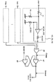
- 단자에 접속된 부하의 부하량을 측정하고, 그 부하량이 기준 부하와 거의 일치할 때, 제어 신호를 출력하는 부하 검지 수단과,상기 제어 신호에 응답하여, 상기 단자로부터 데이터 출력을 정지하거나, 상기 단자에 특정한 논리를 출력하는 출력 제어 수단을 구비하는 것을 특징으로 하는 반도체 장치.
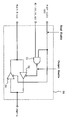
- 제1항에 있어서,상기 부하 검지 수단은,상기 기준 부하를 출력하는 기준 부하 출력 수단과,측정된 상기 부하량과 상기 기준 부하 출력 수단으로부터의 상기 부하량을 비교하고, 그 비교 결과에 따라서 상기 제어 신호를 출력하는 비교 수단을 구비하는 것을 특징으로 하는 반도체 장치.
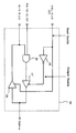
- 제1항에 있어서,상기 부하 검지 수단에는,디지털화된 상기 기준 부하를 출력하는 기준 레지스터와,측정된 상기 부하량을 디지털 변환하는 디지털 변환 수단과,디지털 변환된 상기 부하량과 상기 기준 레지스터로부터의 상기 기준 부하를 비교하고, 그 비교 결과에 따라서 상기 제어 신호를 출력하는 비교 수단을 구비하는 것을 특징으로 하는 반도체 장치.
- 제1항에 있어서,상기 기준 부하는, 상기 데이터를 판독하고 해석하는 해석 장치의 프로브가 상기 단자에 접속되었을 때의 부하량인 것을 특징으로 하는 반도체 장치.
- 단자에 접속된 부하의 부하량을 측정하는 부하 검지 수단과, 상기 단자로부터 데이터를 출력하는 출력 제어 수단을 구비하는 반도체 장치에서의 제어 방법으로서,측정된 상기 부하량이 기준 부하와 거의 일치할 때, 상기 부하 검지 수단으로부터 제어 신호를 출력하고,상기 제어 신호에 응답하여, 상기 출력 제어 수단에 의해서 상기 단자로부터의 상기 데이터의 출력을 정지하거나, 상기 출력 제어 수단으로부터 상기 단자에 특정한 논리를 출력하는 것을 특징으로 하는 제어 방법.
Applications Claiming Priority (2)
| Application Number | Priority Date | Filing Date | Title |
|---|---|---|---|
| JPJP-P-2005-00238617 | 2005-08-19 | ||
| JP2005238617A JP4754903B2 (ja) | 2005-08-19 | 2005-08-19 | 半導体装置、及び半導体装置における制御方法 |
Publications (1)
| Publication Number | Publication Date |
|---|---|
| KR100683096B1 true KR100683096B1 (ko) | 2007-02-16 |
Family
ID=37766567
Family Applications (1)
| Application Number | Title | Priority Date | Filing Date |
|---|---|---|---|
| KR1020050124571A Expired - Fee Related KR100683096B1 (ko) | 2005-08-19 | 2005-12-16 | 반도체 장치 및 반도체 장치에서의 제어 방법 |
Country Status (3)
| Country | Link |
|---|---|
| US (1) | US7614565B2 (ko) |
| JP (1) | JP4754903B2 (ko) |
| KR (1) | KR100683096B1 (ko) |
Families Citing this family (3)
| Publication number | Priority date | Publication date | Assignee | Title |
|---|---|---|---|---|
| GB0223327D0 (en) * | 2002-10-08 | 2002-11-13 | Ranier Ltd | Artificial spinal disc |
| KR101075495B1 (ko) * | 2010-07-06 | 2011-10-21 | 주식회사 하이닉스반도체 | 반도체 모듈에 포함된 다수의 반도체 장치를 선택하는 회로 및 그 동작방법 |
| JP6358497B2 (ja) * | 2014-04-19 | 2018-07-18 | Tianma Japan株式会社 | 制御装置 |
Citations (4)
| Publication number | Priority date | Publication date | Assignee | Title |
|---|---|---|---|---|
| JP2811142B2 (ja) * | 1992-04-30 | 1998-10-15 | アツデン株式会社 | 消費電力管理システム |
| KR20030026551A (ko) * | 2001-09-26 | 2003-04-03 | 삼성전자주식회사 | 메모리 칩의 출력 구동회로 보정 기능을 구비한 메모리 모듈 |
| JP2005027420A (ja) | 2003-07-02 | 2005-01-27 | Fuji Electric Fa Components & Systems Co Ltd | 電動機の駆動制御装置 |
| KR20050022625A (ko) * | 2003-08-29 | 2005-03-08 | 삼성전자주식회사 | 데이터 저장 시스템에서의 데이터 보호 방법 및 이를이용한 디스크 드라이브 |
Family Cites Families (14)
| Publication number | Priority date | Publication date | Assignee | Title |
|---|---|---|---|---|
| JPS63208145A (ja) * | 1987-02-25 | 1988-08-29 | Hitachi Ltd | Icカ−ド |
| EP0509567A3 (en) | 1991-03-28 | 1993-04-07 | N.V. Philips' Gloeilampenfabrieken | Device with protection against access to secure information |
| JP3654938B2 (ja) * | 1994-09-20 | 2005-06-02 | 大日本印刷株式会社 | 電話機 |
| JP3479390B2 (ja) | 1995-06-30 | 2003-12-15 | 沖電気工業株式会社 | 機密性データの解読防止方法と情報処理装置 |
| JP4212068B2 (ja) | 1997-05-19 | 2009-01-21 | ローム株式会社 | Icカードおよびicチップモジュール |
| JPH11120309A (ja) * | 1997-10-15 | 1999-04-30 | Hitachi Ltd | 耐改竄機能付通信装置 |
| JP3641135B2 (ja) | 1998-05-20 | 2005-04-20 | 日本電信電話株式会社 | Icカード |
| JP2000347848A (ja) * | 1999-03-30 | 2000-12-15 | Sony Corp | 半導体ic、情報処理方法、情報処理装置、並びにプログラム格納媒体 |
| JP2001195307A (ja) | 2000-01-06 | 2001-07-19 | Nippon Telegr & Teleph Corp <Ntt> | 半導体装置 |
| JP2001202167A (ja) | 2000-01-20 | 2001-07-27 | Toyo Commun Equip Co Ltd | コンピュータ及びその制御方法 |
| JP2002073422A (ja) | 2000-09-05 | 2002-03-12 | Sharp Corp | 情報処理装置 |
| JP3983521B2 (ja) * | 2001-11-14 | 2007-09-26 | シャープ株式会社 | 半導体装置およびicカード |
| DE60310139T2 (de) * | 2003-01-14 | 2007-09-27 | Koninklijke Philips Electronics N.V. | Erkennung von manipulation an einer chipkartenschnittstelle |
| JP4103753B2 (ja) * | 2003-09-19 | 2008-06-18 | 日産自動車株式会社 | エンジンの排気浄化装置 |
-
2005
- 2005-08-19 JP JP2005238617A patent/JP4754903B2/ja not_active Expired - Fee Related
- 2005-11-28 US US11/287,231 patent/US7614565B2/en not_active Expired - Fee Related
- 2005-12-16 KR KR1020050124571A patent/KR100683096B1/ko not_active Expired - Fee Related
Patent Citations (4)
| Publication number | Priority date | Publication date | Assignee | Title |
|---|---|---|---|---|
| JP2811142B2 (ja) * | 1992-04-30 | 1998-10-15 | アツデン株式会社 | 消費電力管理システム |
| KR20030026551A (ko) * | 2001-09-26 | 2003-04-03 | 삼성전자주식회사 | 메모리 칩의 출력 구동회로 보정 기능을 구비한 메모리 모듈 |
| JP2005027420A (ja) | 2003-07-02 | 2005-01-27 | Fuji Electric Fa Components & Systems Co Ltd | 電動機の駆動制御装置 |
| KR20050022625A (ko) * | 2003-08-29 | 2005-03-08 | 삼성전자주식회사 | 데이터 저장 시스템에서의 데이터 보호 방법 및 이를이용한 디스크 드라이브 |
Also Published As
| Publication number | Publication date |
|---|---|
| US7614565B2 (en) | 2009-11-10 |
| JP4754903B2 (ja) | 2011-08-24 |
| US20070040038A1 (en) | 2007-02-22 |
| JP2007052709A (ja) | 2007-03-01 |
Similar Documents
| Publication | Publication Date | Title |
|---|---|---|
| US7837110B1 (en) | Magnetic stripe reader having digital peak detector | |
| US6059191A (en) | Chip card | |
| US20110202709A1 (en) | Optimizing storage of common patterns in flash memory | |
| US8316242B2 (en) | Cryptoprocessor with improved data protection | |
| US8627116B2 (en) | Power conservation in an intrusion detection system | |
| KR100296199B1 (ko) | 메모리 카드 | |
| US6499092B1 (en) | Method and apparatus for performing access censorship in a data processing system | |
| US7551098B1 (en) | Point of sale terminal having pulsed current tamper control sensing | |
| KR100683096B1 (ko) | 반도체 장치 및 반도체 장치에서의 제어 방법 | |
| KR970076884A (ko) | 반도체 메모리 장치의 멀티비트 테스트 회로 및 그 테스트 방법 | |
| US7420866B2 (en) | Method and system of operating mode detection | |
| US7183792B2 (en) | Method and system for detecting a mode of operation of an integrated circuit, and a memory device including same | |
| US20050157565A1 (en) | Semiconductor device for detecting memory failure and method thereof | |
| US8495443B1 (en) | Secure register scan bypass | |
| US20070282568A1 (en) | Sensor control circuit | |
| US11327882B2 (en) | Method and apparatus for eliminating bit disturbance errors in non-volatile memory devices | |
| US8589749B1 (en) | Memory content protection during scan dumps and memory dumps | |
| CN1251183A (zh) | 集成电路及该集成电路的测试方法 | |
| JP2009036782A (ja) | 携帯型機器の落下衝突を判定する方法 | |
| JP4202116B2 (ja) | メモリ制御回路、メモリ装置およびマイクロコンピュータ | |
| CN101770810B (zh) | 具有多个动作模式的半导体装置 | |
| US20070247182A1 (en) | Protection of security key information | |
| KR100222576B1 (ko) | 아이씨 카드 회로 및 이의 테스트 방법 | |
| US7340313B2 (en) | Monitoring device for monitoring internal signals during initialization of an electronic circuit | |
| JP2006172384A (ja) | 半導体装置 |
Legal Events
| Date | Code | Title | Description |
|---|---|---|---|
| A201 | Request for examination | ||
| PA0109 | Patent application |
St.27 status event code: A-0-1-A10-A12-nap-PA0109 |
|
| PA0201 | Request for examination |
St.27 status event code: A-1-2-D10-D11-exm-PA0201 |
|
| D13-X000 | Search requested |
St.27 status event code: A-1-2-D10-D13-srh-X000 |
|
| D14-X000 | Search report completed |
St.27 status event code: A-1-2-D10-D14-srh-X000 |
|
| E701 | Decision to grant or registration of patent right | ||
| PE0701 | Decision of registration |
St.27 status event code: A-1-2-D10-D22-exm-PE0701 |
|
| GRNT | Written decision to grant | ||
| PR0701 | Registration of establishment |
St.27 status event code: A-2-4-F10-F11-exm-PR0701 |
|
| PR1002 | Payment of registration fee |
St.27 status event code: A-2-2-U10-U11-oth-PR1002 Fee payment year number: 1 |
|
| PG1601 | Publication of registration |
St.27 status event code: A-4-4-Q10-Q13-nap-PG1601 |
|
| R17-X000 | Change to representative recorded |
St.27 status event code: A-5-5-R10-R17-oth-X000 |
|
| PR1001 | Payment of annual fee |
St.27 status event code: A-4-4-U10-U11-oth-PR1001 Fee payment year number: 4 |
|
| PR1001 | Payment of annual fee |
St.27 status event code: A-4-4-U10-U11-oth-PR1001 Fee payment year number: 5 |
|
| PR1001 | Payment of annual fee |
St.27 status event code: A-4-4-U10-U11-oth-PR1001 Fee payment year number: 6 |
|
| FPAY | Annual fee payment |
Payment date: 20130118 Year of fee payment: 7 |
|
| PR1001 | Payment of annual fee |
St.27 status event code: A-4-4-U10-U11-oth-PR1001 Fee payment year number: 7 |
|
| FPAY | Annual fee payment |
Payment date: 20140117 Year of fee payment: 8 |
|
| PR1001 | Payment of annual fee |
St.27 status event code: A-4-4-U10-U11-oth-PR1001 Fee payment year number: 8 |
|
| FPAY | Annual fee payment |
Payment date: 20150119 Year of fee payment: 9 |
|
| PR1001 | Payment of annual fee |
St.27 status event code: A-4-4-U10-U11-oth-PR1001 Fee payment year number: 9 |
|
| FPAY | Annual fee payment |
Payment date: 20160119 Year of fee payment: 10 |
|
| PR1001 | Payment of annual fee |
St.27 status event code: A-4-4-U10-U11-oth-PR1001 Fee payment year number: 10 |
|
| FPAY | Annual fee payment |
Payment date: 20170119 Year of fee payment: 11 |
|
| PR1001 | Payment of annual fee |
St.27 status event code: A-4-4-U10-U11-oth-PR1001 Fee payment year number: 11 |
|
| LAPS | Lapse due to unpaid annual fee | ||
| PC1903 | Unpaid annual fee |
St.27 status event code: A-4-4-U10-U13-oth-PC1903 Not in force date: 20180209 Payment event data comment text: Termination Category : DEFAULT_OF_REGISTRATION_FEE |
|
| PC1903 | Unpaid annual fee |
St.27 status event code: N-4-6-H10-H13-oth-PC1903 Ip right cessation event data comment text: Termination Category : DEFAULT_OF_REGISTRATION_FEE Not in force date: 20180209 |