KR20120024924A - 반도체 장치 - Google Patents
반도체 장치 Download PDFInfo
- Publication number
- KR20120024924A KR20120024924A KR1020120018642A KR20120018642A KR20120024924A KR 20120024924 A KR20120024924 A KR 20120024924A KR 1020120018642 A KR1020120018642 A KR 1020120018642A KR 20120018642 A KR20120018642 A KR 20120018642A KR 20120024924 A KR20120024924 A KR 20120024924A
- Authority
- KR
- South Korea
- Prior art keywords
- layer
- electrode
- common
- insulating layer
- memory
- Prior art date
- Legal status (The legal status is an assumption and is not a legal conclusion. Google has not performed a legal analysis and makes no representation as to the accuracy of the status listed.)
- Granted
Links
Images


Classifications
-
- B—PERFORMING OPERATIONS; TRANSPORTING
- B82—NANOTECHNOLOGY
- B82Y—SPECIFIC USES OR APPLICATIONS OF NANOSTRUCTURES; MEASUREMENT OR ANALYSIS OF NANOSTRUCTURES; MANUFACTURE OR TREATMENT OF NANOSTRUCTURES
- B82Y10/00—Nanotechnology for information processing, storage or transmission, e.g. quantum computing or single electron logic
-
- G—PHYSICS
- G11—INFORMATION STORAGE
- G11C—STATIC STORES
- G11C11/00—Digital stores characterised by the use of particular electric or magnetic storage elements; Storage elements therefor
- G11C11/56—Digital stores characterised by the use of particular electric or magnetic storage elements; Storage elements therefor using storage elements with more than two stable states represented by steps, e.g. of voltage, current, phase, frequency
- G11C11/5664—Digital stores characterised by the use of particular electric or magnetic storage elements; Storage elements therefor using storage elements with more than two stable states represented by steps, e.g. of voltage, current, phase, frequency using organic memory material storage elements
-
- G—PHYSICS
- G11—INFORMATION STORAGE
- G11C—STATIC STORES
- G11C13/00—Digital stores characterised by the use of storage elements not covered by groups G11C11/00, G11C23/00, or G11C25/00
- G11C13/0002—Digital stores characterised by the use of storage elements not covered by groups G11C11/00, G11C23/00, or G11C25/00 using resistive RAM [RRAM] elements
- G11C13/0009—RRAM elements whose operation depends upon chemical change
- G11C13/0014—RRAM elements whose operation depends upon chemical change comprising cells based on organic memory material
-
- H—ELECTRICITY
- H10—SEMICONDUCTOR DEVICES; ELECTRIC SOLID-STATE DEVICES NOT OTHERWISE PROVIDED FOR
- H10D—INORGANIC ELECTRIC SEMICONDUCTOR DEVICES
- H10D86/00—Integrated devices formed in or on insulating or conducting substrates, e.g. formed in silicon-on-insulator [SOI] substrates or on stainless steel or glass substrates
- H10D86/01—Manufacture or treatment
- H10D86/021—Manufacture or treatment of multiple TFTs
- H10D86/0214—Manufacture or treatment of multiple TFTs using temporary substrates
-
- H—ELECTRICITY
- H10—SEMICONDUCTOR DEVICES; ELECTRIC SOLID-STATE DEVICES NOT OTHERWISE PROVIDED FOR
- H10D—INORGANIC ELECTRIC SEMICONDUCTOR DEVICES
- H10D86/00—Integrated devices formed in or on insulating or conducting substrates, e.g. formed in silicon-on-insulator [SOI] substrates or on stainless steel or glass substrates
- H10D86/40—Integrated devices formed in or on insulating or conducting substrates, e.g. formed in silicon-on-insulator [SOI] substrates or on stainless steel or glass substrates characterised by multiple TFTs
-
- H—ELECTRICITY
- H10—SEMICONDUCTOR DEVICES; ELECTRIC SOLID-STATE DEVICES NOT OTHERWISE PROVIDED FOR
- H10D—INORGANIC ELECTRIC SEMICONDUCTOR DEVICES
- H10D86/00—Integrated devices formed in or on insulating or conducting substrates, e.g. formed in silicon-on-insulator [SOI] substrates or on stainless steel or glass substrates
- H10D86/80—Integrated devices formed in or on insulating or conducting substrates, e.g. formed in silicon-on-insulator [SOI] substrates or on stainless steel or glass substrates characterised by multiple passive components, e.g. resistors, capacitors or inductors
-
- H—ELECTRICITY
- H10—SEMICONDUCTOR DEVICES; ELECTRIC SOLID-STATE DEVICES NOT OTHERWISE PROVIDED FOR
- H10K—ORGANIC ELECTRIC SOLID-STATE DEVICES
- H10K10/00—Organic devices specially adapted for rectifying, amplifying, oscillating or switching; Organic capacitors or resistors having potential barriers
- H10K10/701—Organic molecular electronic devices
-
- H—ELECTRICITY
- H10—SEMICONDUCTOR DEVICES; ELECTRIC SOLID-STATE DEVICES NOT OTHERWISE PROVIDED FOR
- H10D—INORGANIC ELECTRIC SEMICONDUCTOR DEVICES
- H10D86/00—Integrated devices formed in or on insulating or conducting substrates, e.g. formed in silicon-on-insulator [SOI] substrates or on stainless steel or glass substrates
- H10D86/40—Integrated devices formed in or on insulating or conducting substrates, e.g. formed in silicon-on-insulator [SOI] substrates or on stainless steel or glass substrates characterised by multiple TFTs
- H10D86/481—Integrated devices formed in or on insulating or conducting substrates, e.g. formed in silicon-on-insulator [SOI] substrates or on stainless steel or glass substrates characterised by multiple TFTs integrated with passive devices, e.g. auxiliary capacitors
-
- H—ELECTRICITY
- H10—SEMICONDUCTOR DEVICES; ELECTRIC SOLID-STATE DEVICES NOT OTHERWISE PROVIDED FOR
- H10D—INORGANIC ELECTRIC SEMICONDUCTOR DEVICES
- H10D86/00—Integrated devices formed in or on insulating or conducting substrates, e.g. formed in silicon-on-insulator [SOI] substrates or on stainless steel or glass substrates
- H10D86/40—Integrated devices formed in or on insulating or conducting substrates, e.g. formed in silicon-on-insulator [SOI] substrates or on stainless steel or glass substrates characterised by multiple TFTs
- H10D86/60—Integrated devices formed in or on insulating or conducting substrates, e.g. formed in silicon-on-insulator [SOI] substrates or on stainless steel or glass substrates characterised by multiple TFTs wherein the TFTs are in active matrices
Landscapes
- Engineering & Computer Science (AREA)
- Nanotechnology (AREA)
- Chemical & Material Sciences (AREA)
- Computer Hardware Design (AREA)
- Physics & Mathematics (AREA)
- Theoretical Computer Science (AREA)
- Crystallography & Structural Chemistry (AREA)
- Mathematical Physics (AREA)
- Spectroscopy & Molecular Physics (AREA)
- Semiconductor Memories (AREA)
- Thin Film Transistor (AREA)
- Dram (AREA)
- Electroluminescent Light Sources (AREA)
Abstract
Description
도 2a 및 2b는 본 발명의 반도체 장치의 제조 단계를 도시하는 도면들.
도 3은 본 발명의 반도체 장치의 제조 단계를 도시하는 도면.
도 4a 및 4b는 본 발명의 반도체 장치의 제조 단계를 도시하는 도면들.
도 5a 및 5b는 실시 형태 2의 반도체 장치의 제조 단계를 도시하는 도면들.
도 6a 및 6b는 실시 형태 2의 반도체 장치의 제조 단계를 도시하는 도면들.
도 7은 실시 형태 2의 반도체 장치의 제조 단계를 도시하는 도면.
도 8a 및 8b는 실시 형태 2의 반도체 장치의 제조 단계를 도시하는 도면들.
도 9a 및 9b는 실시 형태 3의 반도체 장치의 제조 단계를 도시하는 도면들.
도 10은 실시 형태 3의 반도체 장치의 제조 단계를 도시하는 도면.
도 11a 및 11b는 실시 형태 4의 반도체 장치의 제조 단계를 도시하는 도면들.
도 12a 및 12b는 실시 형태 4의 반도체 장치의 제조 단계를 도시하는 도면들.
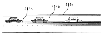
도 13a 및 13c는 실시 형태 2의 반도체 장치의 상면도들.
도 13b는 실시 형태 2의 반도체 장치의 단면도.
도 14a 내지 14c는 실시 형태 5의 반도체 장치의 제조 단계를 도시하는 도면들.
도 15a 및 15b는 실시 형태 5의 반도체 장치의 제조 단계를 도시하는 도면들.
도 16a는 본 발명의 반도체 장치의 구성예를 도시하는 도면.
도 16b는 본 발명의 반도체 장치를 포함하는 전자 장치를 도시하는 도면.
도 17a 및 17b는 본 발명의 반도체 장치를 포함하는 전자 장치를 도시하는 도면들.
도 18a 내지 18f는 본 발명의 반도체 장치의 용도를 도시하는 도면들.


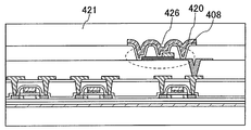
401 : 유리 기판 402 : 분리층
403 : 절연층 405 : 게이트 절연층
406 : 게이트 전극층 407 : 불순물 영역
415 : 도전층 416 : 절연층
Claims (14)
- 공통의 제 1 전극;
공통의 제 2 전극; 및
상기 공통의 제 1 전극과 상기 공통의 제 2 전극 사이의 공통의 재료층을 포함하고,
상기 공통의 제 1 전극은 최하층 및 최상층을 포함하는 적층 구조를 갖고,
상기 최하층의 면적은 상기 최상층의 면적보다 큰, 반도체 장치. - 제 1 항에 있어서,
상기 공통의 제 1 전극과 겹치는 제 1 개구부, 제 2 개구부, 및 제 3 개구부가 적어도 설치된 절연층을 더 포함하고,
상기 절연층은 상기 공통의 제 1 전극과 상기 공통의 재료층 사이에 위치하는, 반도체 장치. - 공통의 제 1 전극;
공통의 제 2 전극; 및
상기 공통의 제 1 전극과 상기 공통의 제 2 전극 사이의 공통의 재료층을 포함하고,
상기 공통의 제 1 전극은 최하층 및 최상층을 포함하는 적층 구조를 갖고,
상기 최하층의 단부는 상기 최상층의 단부를 넘어 확장하는, 반도체 장치. - 제 3 항에 있어서,
상기 공통의 제 1 전극과 겹치는 제 1 개구부, 제 2 개구부, 및 제 3 개구부가 적어도 설치된 절연층을 더 포함하고,
상기 절연층은 상기 공통의 제 1 전극과 상기 공통의 재료층 사이에 위치하는, 반도체 장치. - 제 4 항에 있어서,
상기 최하층의 상기 단부는 상기 제 1 개구부에 위치하고,
상기 최상층의 상기 단부는 상기 제 2 개구부에 위치하는, 반도체 장치. - 공통의 제 1 전극;
공통의 제 2 전극; 및
상기 공통의 제 1 전극과 상기 공통의 제 2 전극 사이의 공통의 재료층을 포함하고,
상기 공통의 제 1 전극은 최하층 및 최상층을 포함하는 적층 구조를 갖고,
상기 최하층의 막 두께는 상기 최상층의 막 두께와 다른, 반도체 장치. - 제 6 항에 있어서,
상기 공통의 제 1 전극과 겹치는 제 1 개구부, 제 2 개구부, 및 제 3 개구부가 적어도 설치된 절연층을 더 포함하고,
상기 절연층은 상기 공통의 제 1 전극과 상기 공통의 재료층 사이에 위치하는, 반도체 장치. - 제 2 항 또는 제 7 항에 있어서,
상기 최하층의 단부는 상기 제 1 개구부에 위치하고,
상기 최상층의 단부는 상기 제 2 개구부에 위치하는, 반도체 장치. - 제 2 항, 제 4 항, 및 제 7 항 중 어느 한 항에 있어서,
상기 제 1 개구부, 상기 제 2 개구부, 및 상기 제 3 개구부의 단위 면적당 기억 용량들은 서로 다른, 반도체 장치. - 제 2 항, 제 4 항, 및 제 7 항 중 어느 한 항에 있어서,
상기 제 1 개구부, 상기 제 2 개구부, 및 상기 제 3 개구부 각각에서, 전기 저항은 전압의 인가로 인해 변화하고,
상기 제 1 개구부에서 상기 전기 저항이 변화하는 전압 값은 상기 제 2 개구부 및 상기 제 3 개구부에서 상기 전기 저항들이 변화하는 전압 값들과 다른, 반도체 장치. - 제 7 항에 있어서,
상기 제 1 개구부에서, 상기 최하층의 단부, 상기 공통의 재료층, 및 상기 공통의 제 2 전극은 겹치고,
상기 제 2 개구부에서, 상기 최하층, 상기 최상층의 단부, 상기 공통의 재료층, 및 상기 공통의 제 2 전극은 겹치고,
상기 제 3 개구부에서, 상기 최하층, 상기 최상층, 상기 공통의 재료층, 및 상기 공통의 제 2 전극은 겹치는, 반도체 장치. - 공통의 제 1 전극;
공통의 제 2 전극; 및
상기 공통의 제 1 전극과 상기 공통의 제 2 전극 사이의 공통의 재료층을 포함하고,
상기 공통의 제 1 전극은 최하층 및 최상층을 포함하는 적층 구조를 갖고,
제 1 영역에서, 상기 최하층의 단부, 상기 공통의 재료층, 및 상기 공통의 제 2 전극은 겹치고,
제 2 영역에서, 상기 최하층, 상기 최상층의 단부, 상기 공통의 재료층, 및 상기 공통의 제 2 전극은 겹치고,
제 3 영역에서, 상기 최하층, 상기 최상층, 상기 공통의 재료층, 및 상기 공통의 제 2 전극은 겹치는, 반도체 장치. - 제 1 항, 제 3 항, 제 6 항, 및 제 12 항 중 어느 한 항에 있어서,
메모리 셀은 상기 공통의 제 1 전극, 상기 공통의 제 2 전극, 및 상기 공통의 재료층을 포함하는, 반도체 장치. - 제 1 항, 제 3 항, 제 6 항, 및 제 12 항 중 어느 한 항에 있어서,
상기 최상층의 측면의 테이퍼 각은 상기 최하층의 측면의 테이퍼 각과 다른, 반도체 장치.
Applications Claiming Priority (2)
| Application Number | Priority Date | Filing Date | Title |
|---|---|---|---|
| JPJP-P-2006-047057 | 2006-02-23 | ||
| JP2006047057 | 2006-02-23 |
Related Parent Applications (1)
| Application Number | Title | Priority Date | Filing Date |
|---|---|---|---|
| KR1020070018403A Division KR101350204B1 (ko) | 2006-02-23 | 2007-02-23 | 반도체 장치 |
Publications (2)
| Publication Number | Publication Date |
|---|---|
| KR20120024924A true KR20120024924A (ko) | 2012-03-14 |
| KR101420606B1 KR101420606B1 (ko) | 2014-07-17 |
Family
ID=38068872
Family Applications (2)
| Application Number | Title | Priority Date | Filing Date |
|---|---|---|---|
| KR1020070018403A Expired - Fee Related KR101350204B1 (ko) | 2006-02-23 | 2007-02-23 | 반도체 장치 |
| KR1020120018642A Expired - Fee Related KR101420606B1 (ko) | 2006-02-23 | 2012-02-23 | 반도체 장치 |
Family Applications Before (1)
| Application Number | Title | Priority Date | Filing Date |
|---|---|---|---|
| KR1020070018403A Expired - Fee Related KR101350204B1 (ko) | 2006-02-23 | 2007-02-23 | 반도체 장치 |
Country Status (6)
| Country | Link |
|---|---|
| US (2) | US7605410B2 (ko) |
| EP (1) | EP1826818A3 (ko) |
| JP (1) | JP5459916B2 (ko) |
| KR (2) | KR101350204B1 (ko) |
| CN (2) | CN101026163B (ko) |
| TW (1) | TWI430433B (ko) |
Families Citing this family (24)
| Publication number | Priority date | Publication date | Assignee | Title |
|---|---|---|---|---|
| DE10260149A1 (de) | 2002-12-20 | 2004-07-01 | BSH Bosch und Siemens Hausgeräte GmbH | Vorrichtung zur Bestimmung des Leitwertes von Wäsche, Wäschetrockner und Verfahren zur Verhinderung von Schichtbildung auf Elektroden |
| US8193606B2 (en) * | 2005-02-28 | 2012-06-05 | Semiconductor Energy Laboratory Co., Ltd. | Semiconductor device including a memory element |
| US7719872B2 (en) * | 2005-12-28 | 2010-05-18 | Semiconductor Energy Laboratory Co., Ltd. | Write-once nonvolatile memory with redundancy capability |
| JP5352081B2 (ja) * | 2006-12-20 | 2013-11-27 | 株式会社半導体エネルギー研究所 | 半導体装置の作製方法 |
| WO2010032602A1 (en) | 2008-09-18 | 2010-03-25 | Semiconductor Energy Laboratory Co., Ltd. | Semiconductor device |
| WO2010032599A1 (en) | 2008-09-19 | 2010-03-25 | Semiconductor Energy Laboratory Co., Ltd. | Semiconductor device |
| WO2010032611A1 (en) | 2008-09-19 | 2010-03-25 | Semiconductor Energy Laboratory Co., Ltd. | Semiconductor device and method for manufacturing the same |
| JP5586920B2 (ja) * | 2008-11-20 | 2014-09-10 | 株式会社半導体エネルギー研究所 | フレキシブル半導体装置の作製方法 |
| US8911653B2 (en) | 2009-05-21 | 2014-12-16 | Semiconductor Energy Laboratory Co., Ltd. | Method for manufacturing light-emitting device |
| CN105590646B (zh) * | 2009-12-25 | 2019-01-08 | 株式会社半导体能源研究所 | 存储器装置、半导体器件和电子装置 |
| KR101030031B1 (ko) | 2010-01-08 | 2011-04-20 | 삼성모바일디스플레이주식회사 | 유기전계발광표시장치 및 그의 제조방법 |
| WO2011089835A1 (en) * | 2010-01-20 | 2011-07-28 | Semiconductor Energy Laboratory Co., Ltd. | Semiconductor memory device |
| KR101924231B1 (ko) | 2010-10-29 | 2018-11-30 | 가부시키가이샤 한도오따이 에네루기 켄큐쇼 | 반도체 기억 장치 |
| US8854865B2 (en) | 2010-11-24 | 2014-10-07 | Semiconductor Energy Laboratory Co., Ltd. | Semiconductor memory device |
| US8614488B2 (en) * | 2010-12-08 | 2013-12-24 | Ying-Nan Wen | Chip package and method for forming the same |
| KR102568895B1 (ko) | 2014-03-13 | 2023-08-21 | 가부시키가이샤 한도오따이 에네루기 켄큐쇼 | 전자 장치 |
| CN104409627A (zh) * | 2014-10-30 | 2015-03-11 | 北京大学 | 一种小尺寸超薄阻变存储器及其制备方法 |
| US10186311B2 (en) * | 2015-05-07 | 2019-01-22 | Semiconductor Energy Laboratory Co., Ltd. | Semiconductor device or electronic component including the same |
| US9728243B2 (en) | 2015-05-11 | 2017-08-08 | Semiconductor Energy Laboratory Co., Ltd. | Semiconductor device or electronic component including the same |
| JP6901831B2 (ja) | 2015-05-26 | 2021-07-14 | 株式会社半導体エネルギー研究所 | メモリシステム、及び情報処理システム |
| KR102499288B1 (ko) * | 2016-01-08 | 2023-02-14 | 삼성디스플레이 주식회사 | 표시 장치 |
| CN106298803A (zh) * | 2016-08-18 | 2017-01-04 | 深圳市华星光电技术有限公司 | 阵列基板及其制作方法、液晶显示面板 |
| KR102565380B1 (ko) * | 2016-12-07 | 2023-08-10 | 삼성디스플레이 주식회사 | 박막 트랜지스터 기판 |
| US10210920B1 (en) | 2018-03-27 | 2019-02-19 | Qualcomm Incorporated | Magnetic tunnel junction (MTJ) devices with varied breakdown voltages in different memory arrays fabricated in a same semiconductor die to facilitate different memory applications |
Family Cites Families (44)
| Publication number | Priority date | Publication date | Assignee | Title |
|---|---|---|---|---|
| US4809044A (en) * | 1986-08-22 | 1989-02-28 | Energy Conversion Devices, Inc. | Thin film overvoltage protection devices |
| US4845533A (en) * | 1986-08-22 | 1989-07-04 | Energy Conversion Devices, Inc. | Thin film electrical devices with amorphous carbon electrodes and method of making same |
| JPH01278065A (ja) * | 1988-04-28 | 1989-11-08 | Hitachi Ltd | 半導体記憶装置 |
| CA2022929C (en) * | 1989-08-10 | 1995-02-07 | Hisaaki Kawade | Organic recording medium with electrodes |
| US5541441A (en) * | 1994-10-06 | 1996-07-30 | Actel Corporation | Metal to metal antifuse |
| JP3169599B2 (ja) * | 1990-08-03 | 2001-05-28 | 株式会社日立製作所 | 半導体装置、その駆動方法、その読み出し方法 |
| WO1992020095A1 (en) * | 1991-04-26 | 1992-11-12 | Quicklogic Corporation | Programmable interconnect structures and programmable integrated circuits |
| JP2794348B2 (ja) * | 1991-06-21 | 1998-09-03 | キヤノン株式会社 | 記録媒体、その製造方法、情報処理装置 |
| JPH0955476A (ja) * | 1995-08-10 | 1997-02-25 | Seiko Epson Corp | 半導体装置 |
| EP0821826B1 (en) * | 1996-02-16 | 2003-07-23 | Koninklijke Philips Electronics N.V. | Write-once read-many electrical memory element of a conjugated polymer or oligomer |
| JPH09266253A (ja) * | 1996-03-28 | 1997-10-07 | Seiko Epson Corp | 半導体装置 |
| US6288423B1 (en) * | 1997-04-18 | 2001-09-11 | Nippon Steel Corporation | Composite gate structure memory cell having increased capacitance |
| NO973993L (no) * | 1997-09-01 | 1999-03-02 | Opticom As | Leseminne og leseminneinnretninger |
| US6034882A (en) * | 1998-11-16 | 2000-03-07 | Matrix Semiconductor, Inc. | Vertically stacked field programmable nonvolatile memory and method of fabrication |
| US6288437B1 (en) * | 1999-02-26 | 2001-09-11 | Micron Technology, Inc. | Antifuse structures methods and applications |
| JP2001189431A (ja) | 1999-12-28 | 2001-07-10 | Seiko Epson Corp | メモリのセル構造及びメモリデバイス |
| JP2001345431A (ja) | 2000-05-31 | 2001-12-14 | Japan Science & Technology Corp | 有機強誘電体薄膜及び半導体デバイス |
| JP2002026283A (ja) | 2000-06-30 | 2002-01-25 | Seiko Epson Corp | 多層構造のメモリ装置及びその製造方法 |
| DE10045192A1 (de) * | 2000-09-13 | 2002-04-04 | Siemens Ag | Organischer Datenspeicher, RFID-Tag mit organischem Datenspeicher, Verwendung eines organischen Datenspeichers |
| WO2002037500A1 (en) * | 2000-10-31 | 2002-05-10 | The Regents Of The University Of California | Organic bistable device and organic memory cells |
| US6498056B1 (en) * | 2000-10-31 | 2002-12-24 | International Business Machines Corporation | Apparatus and method for antifuse with electrostatic assist |
| US7087975B2 (en) * | 2000-12-28 | 2006-08-08 | Infineon Technologies Ag | Area efficient stacking of antifuses in semiconductor device |
| WO2002091384A1 (en) * | 2001-05-07 | 2002-11-14 | Advanced Micro Devices, Inc. | A memory device with a self-assembled polymer film and method of making the same |
| US6762445B2 (en) * | 2001-07-19 | 2004-07-13 | Matsushita Electric Industrial Co., Ltd. | DRAM memory cell with dummy lower electrode for connection between upper electrode and upper layer interconnect |
| DE60130586T2 (de) * | 2001-08-13 | 2008-06-19 | Advanced Micro Devices, Inc., Sunnyvale | Speicherzelle |
| US6465282B1 (en) * | 2001-09-28 | 2002-10-15 | Infineon Technologies Ag | Method of forming a self-aligned antifuse link |
| US7196422B2 (en) * | 2001-12-14 | 2007-03-27 | Intel Corporation | Low-dielectric constant structure with a multilayer stack of thin films with pores |
| US6686236B2 (en) * | 2001-12-21 | 2004-02-03 | Texas Instruments Incorporated | Methods of preventing reduction of IrOx during PZT formation by metalorganic chemical vapor deposition or other processing |
| DE10210044A1 (de) * | 2002-03-07 | 2003-09-18 | Philips Intellectual Property | Integrierte monolithische SOI-Schaltung mit Kondensator |
| US6979387B2 (en) * | 2002-03-08 | 2005-12-27 | Ichikawa Co., Ltd. | Doctor blade for removing water |
| US6943065B2 (en) * | 2002-03-25 | 2005-09-13 | Micron Technology Inc. | Scalable high performance antifuse structure and process |
| US6828685B2 (en) * | 2002-06-14 | 2004-12-07 | Hewlett-Packard Development Company, L.P. | Memory device having a semiconducting polymer film |
| US7075105B2 (en) * | 2003-03-19 | 2006-07-11 | Masataka Kano | Organic bistable element, organic bistable memory device using the same, and method for driving said organic bistable element and organic bistable memory device |
| US6977389B2 (en) * | 2003-06-02 | 2005-12-20 | Advanced Micro Devices, Inc. | Planar polymer memory device |
| JP4545397B2 (ja) | 2003-06-19 | 2010-09-15 | 株式会社 日立ディスプレイズ | 画像表示装置 |
| US20050006640A1 (en) * | 2003-06-26 | 2005-01-13 | Jackson Warren B. | Polymer-based memory element |
| US6803267B1 (en) * | 2003-07-07 | 2004-10-12 | Advanced Micro Devices, Inc. | Silicon containing material for patterning polymeric memory element |
| JP4836466B2 (ja) * | 2004-02-06 | 2011-12-14 | 株式会社半導体エネルギー研究所 | 半導体装置 |
| TWI277207B (en) * | 2004-10-08 | 2007-03-21 | Ind Tech Res Inst | Multilevel phase-change memory, operating method and manufacture method thereof |
| JP2006108645A (ja) | 2004-10-08 | 2006-04-20 | Ind Technol Res Inst | マルチレベル相変化メモリ、及びその動作方法並びに製造方法 |
| TWI254443B (en) * | 2004-10-08 | 2006-05-01 | Ind Tech Res Inst | Multilevel phase-change memory, manufacture method and status transferring method thereof |
| KR100623717B1 (ko) * | 2004-11-15 | 2006-09-19 | 삼성에스디아이 주식회사 | 유기전계 발광소자 및 그 제조 방법 |
| US8193606B2 (en) * | 2005-02-28 | 2012-06-05 | Semiconductor Energy Laboratory Co., Ltd. | Semiconductor device including a memory element |
| US7358590B2 (en) * | 2005-03-31 | 2008-04-15 | Semiconductor Energy Laboratory Co., Ltd. | Semiconductor device and driving method thereof |
-
2007
- 2007-02-05 US US11/702,083 patent/US7605410B2/en not_active Expired - Fee Related
- 2007-02-07 TW TW096104482A patent/TWI430433B/zh not_active IP Right Cessation
- 2007-02-12 EP EP07002951.7A patent/EP1826818A3/en not_active Withdrawn
- 2007-02-23 KR KR1020070018403A patent/KR101350204B1/ko not_active Expired - Fee Related
- 2007-02-25 CN CN2007100058074A patent/CN101026163B/zh not_active Expired - Fee Related
- 2007-02-25 CN CN2010106209648A patent/CN102142443B/zh not_active Expired - Fee Related
-
2009
- 2009-10-14 US US12/578,650 patent/US8642987B2/en not_active Expired - Fee Related
-
2012
- 2012-02-23 KR KR1020120018642A patent/KR101420606B1/ko not_active Expired - Fee Related
- 2012-08-07 JP JP2012174805A patent/JP5459916B2/ja not_active Expired - Fee Related
Also Published As
| Publication number | Publication date |
|---|---|
| KR20070087522A (ko) | 2007-08-28 |
| TW200802806A (en) | 2008-01-01 |
| CN102142443A (zh) | 2011-08-03 |
| KR101350204B1 (ko) | 2014-01-13 |
| KR101420606B1 (ko) | 2014-07-17 |
| CN101026163B (zh) | 2011-02-23 |
| CN102142443B (zh) | 2013-04-03 |
| EP1826818A3 (en) | 2015-04-15 |
| EP1826818A2 (en) | 2007-08-29 |
| JP5459916B2 (ja) | 2014-04-02 |
| US7605410B2 (en) | 2009-10-20 |
| CN101026163A (zh) | 2007-08-29 |
| JP2013016817A (ja) | 2013-01-24 |
| TWI430433B (zh) | 2014-03-11 |
| US20070194323A1 (en) | 2007-08-23 |
| US8642987B2 (en) | 2014-02-04 |
| US20100038618A1 (en) | 2010-02-18 |
Similar Documents
| Publication | Publication Date | Title |
|---|---|---|
| KR101350204B1 (ko) | 반도체 장치 | |
| US8647942B2 (en) | Semiconductor device and manufacturing method thereof | |
| US8088654B2 (en) | Semiconductor device and manufacturing method thereof | |
| KR101187400B1 (ko) | 반도체장치 | |
| US8120159B2 (en) | Semiconductor integrated circuit, manufacturing method thereof, and semiconductor device using semiconductor integrated circuit | |
| CN100565900C (zh) | 半导体器件 | |
| JP5303588B2 (ja) | 半導体装置の作製方法 | |
| JP2008004893A (ja) | 半導体装置及び半導体装置の作製方法 | |
| JP5297591B2 (ja) | 半導体装置 | |
| JP5210656B2 (ja) | 記憶素子及びその作製方法 | |
| JP4939838B2 (ja) | 記憶装置 | |
| JP5190182B2 (ja) | 半導体装置 | |
| JP2008166420A (ja) | 半導体装置 | |
| JP2006179882A (ja) | 半導体装置およびその作製方法 |
Legal Events
| Date | Code | Title | Description |
|---|---|---|---|
| A107 | Divisional application of patent | ||
| A201 | Request for examination | ||
| PA0107 | Divisional application |
St.27 status event code: A-0-1-A10-A16-div-PA0107 St.27 status event code: A-0-1-A10-A18-div-PA0107 |
|
| PA0201 | Request for examination |
St.27 status event code: A-1-2-D10-D11-exm-PA0201 |
|
| PG1501 | Laying open of application |
St.27 status event code: A-1-1-Q10-Q12-nap-PG1501 |
|
| E902 | Notification of reason for refusal | ||
| PE0902 | Notice of grounds for rejection |
St.27 status event code: A-1-2-D10-D21-exm-PE0902 |
|
| E902 | Notification of reason for refusal | ||
| PE0902 | Notice of grounds for rejection |
St.27 status event code: A-1-2-D10-D21-exm-PE0902 |
|
| E701 | Decision to grant or registration of patent right | ||
| PE0701 | Decision of registration |
St.27 status event code: A-1-2-D10-D22-exm-PE0701 |
|
| GRNT | Written decision to grant | ||
| PR0701 | Registration of establishment |
St.27 status event code: A-2-4-F10-F11-exm-PR0701 |
|
| PR1002 | Payment of registration fee |
Fee payment year number: 1 St.27 status event code: A-2-2-U10-U11-oth-PR1002 |
|
| PG1601 | Publication of registration |
St.27 status event code: A-4-4-Q10-Q13-nap-PG1601 |
|
| FPAY | Annual fee payment |
Payment date: 20170616 Year of fee payment: 4 |
|
| PR1001 | Payment of annual fee |
Fee payment year number: 4 St.27 status event code: A-4-4-U10-U11-oth-PR1001 |
|
| PR1001 | Payment of annual fee |
Fee payment year number: 5 St.27 status event code: A-4-4-U10-U11-oth-PR1001 |
|
| FPAY | Annual fee payment |
Payment date: 20190617 Year of fee payment: 6 |
|
| PR1001 | Payment of annual fee |
Fee payment year number: 6 St.27 status event code: A-4-4-U10-U11-oth-PR1001 |
|
| PR1001 | Payment of annual fee |
Fee payment year number: 7 St.27 status event code: A-4-4-U10-U11-oth-PR1001 |
|
| PR1001 | Payment of annual fee |
Fee payment year number: 8 St.27 status event code: A-4-4-U10-U11-oth-PR1001 |
|
| PC1903 | Unpaid annual fee |
Not in force date: 20220712 Payment event data comment text: Termination Category : DEFAULT_OF_REGISTRATION_FEE St.27 status event code: A-4-4-U10-U13-oth-PC1903 |
|
| P22-X000 | Classification modified |
St.27 status event code: A-4-4-P10-P22-nap-X000 |
|
| PC1903 | Unpaid annual fee |
Ip right cessation event data comment text: Termination Category : DEFAULT_OF_REGISTRATION_FEE Not in force date: 20220712 St.27 status event code: N-4-6-H10-H13-oth-PC1903 |
|
| P22-X000 | Classification modified |
St.27 status event code: A-4-4-P10-P22-nap-X000 |