KR20120052925A - 리소그래피 장치 및 리소그래피 장치 클리닝 방법 - Google Patents
리소그래피 장치 및 리소그래피 장치 클리닝 방법 Download PDFInfo
- Publication number
- KR20120052925A KR20120052925A KR1020120050989A KR20120050989A KR20120052925A KR 20120052925 A KR20120052925 A KR 20120052925A KR 1020120050989 A KR1020120050989 A KR 1020120050989A KR 20120050989 A KR20120050989 A KR 20120050989A KR 20120052925 A KR20120052925 A KR 20120052925A
- Authority
- KR
- South Korea
- Prior art keywords
- liquid
- substrate
- projection system
- megasonic
- cleaned
- Prior art date
- Legal status (The legal status is an assumption and is not a legal conclusion. Google has not performed a legal analysis and makes no representation as to the accuracy of the status listed.)
- Ceased
Links
Images



Classifications
-
- H—ELECTRICITY
- H10—SEMICONDUCTOR DEVICES; ELECTRIC SOLID-STATE DEVICES NOT OTHERWISE PROVIDED FOR
- H10P—GENERIC PROCESSES OR APPARATUS FOR THE MANUFACTURE OR TREATMENT OF DEVICES COVERED BY CLASS H10
- H10P76/00—Manufacture or treatment of masks on semiconductor bodies, e.g. by lithography or photolithography
- H10P76/20—Manufacture or treatment of masks on semiconductor bodies, e.g. by lithography or photolithography of masks comprising organic materials
- H10P76/204—Manufacture or treatment of masks on semiconductor bodies, e.g. by lithography or photolithography of masks comprising organic materials of organic photoresist masks
- H10P76/2041—Photolithographic processes
-
- H—ELECTRICITY
- H10—SEMICONDUCTOR DEVICES; ELECTRIC SOLID-STATE DEVICES NOT OTHERWISE PROVIDED FOR
- H10P—GENERIC PROCESSES OR APPARATUS FOR THE MANUFACTURE OR TREATMENT OF DEVICES COVERED BY CLASS H10
- H10P72/00—Handling or holding of wafers, substrates or devices during manufacture or treatment thereof
- H10P72/70—Handling or holding of wafers, substrates or devices during manufacture or treatment thereof for supporting or gripping
- H10P72/76—Handling or holding of wafers, substrates or devices during manufacture or treatment thereof for supporting or gripping using mechanical means, e.g. clamps or pinches
- H10P72/7604—Handling or holding of wafers, substrates or devices during manufacture or treatment thereof for supporting or gripping using mechanical means, e.g. clamps or pinches the wafers being placed on a susceptor, stage or support
- H10P72/7611—Handling or holding of wafers, substrates or devices during manufacture or treatment thereof for supporting or gripping using mechanical means, e.g. clamps or pinches the wafers being placed on a susceptor, stage or support characterised by edge profile or support profile
-
- G—PHYSICS
- G03—PHOTOGRAPHY; CINEMATOGRAPHY; ANALOGOUS TECHNIQUES USING WAVES OTHER THAN OPTICAL WAVES; ELECTROGRAPHY; HOLOGRAPHY
- G03F—PHOTOMECHANICAL PRODUCTION OF TEXTURED OR PATTERNED SURFACES, e.g. FOR PRINTING, FOR PROCESSING OF SEMICONDUCTOR DEVICES; MATERIALS THEREFOR; ORIGINALS THEREFOR; APPARATUS SPECIALLY ADAPTED THEREFOR
- G03F7/00—Photomechanical, e.g. photolithographic, production of textured or patterned surfaces, e.g. printing surfaces; Materials therefor, e.g. comprising photoresists; Apparatus specially adapted therefor
- G03F7/20—Exposure; Apparatus therefor
- G03F7/2041—Exposure; Apparatus therefor in the presence of a fluid, e.g. immersion; using fluid cooling means
-
- G—PHYSICS
- G03—PHOTOGRAPHY; CINEMATOGRAPHY; ANALOGOUS TECHNIQUES USING WAVES OTHER THAN OPTICAL WAVES; ELECTROGRAPHY; HOLOGRAPHY
- G03F—PHOTOMECHANICAL PRODUCTION OF TEXTURED OR PATTERNED SURFACES, e.g. FOR PRINTING, FOR PROCESSING OF SEMICONDUCTOR DEVICES; MATERIALS THEREFOR; ORIGINALS THEREFOR; APPARATUS SPECIALLY ADAPTED THEREFOR
- G03F7/00—Photomechanical, e.g. photolithographic, production of textured or patterned surfaces, e.g. printing surfaces; Materials therefor, e.g. comprising photoresists; Apparatus specially adapted therefor
- G03F7/70—Microphotolithographic exposure; Apparatus therefor
- G03F7/708—Construction of apparatus, e.g. environment aspects, hygiene aspects or materials
- G03F7/70908—Hygiene, e.g. preventing apparatus pollution, mitigating effect of pollution or removing pollutants from apparatus
- G03F7/70916—Pollution mitigation, i.e. mitigating effect of contamination or debris, e.g. foil traps
-
- G—PHYSICS
- G03—PHOTOGRAPHY; CINEMATOGRAPHY; ANALOGOUS TECHNIQUES USING WAVES OTHER THAN OPTICAL WAVES; ELECTROGRAPHY; HOLOGRAPHY
- G03F—PHOTOMECHANICAL PRODUCTION OF TEXTURED OR PATTERNED SURFACES, e.g. FOR PRINTING, FOR PROCESSING OF SEMICONDUCTOR DEVICES; MATERIALS THEREFOR; ORIGINALS THEREFOR; APPARATUS SPECIALLY ADAPTED THEREFOR
- G03F7/00—Photomechanical, e.g. photolithographic, production of textured or patterned surfaces, e.g. printing surfaces; Materials therefor, e.g. comprising photoresists; Apparatus specially adapted therefor
- G03F7/70—Microphotolithographic exposure; Apparatus therefor
- G03F7/708—Construction of apparatus, e.g. environment aspects, hygiene aspects or materials
- G03F7/70908—Hygiene, e.g. preventing apparatus pollution, mitigating effect of pollution or removing pollutants from apparatus
- G03F7/70925—Cleaning, i.e. actively freeing apparatus from pollutants, e.g. using plasma cleaning
Landscapes
- Epidemiology (AREA)
- Health & Medical Sciences (AREA)
- Public Health (AREA)
- Physics & Mathematics (AREA)
- Engineering & Computer Science (AREA)
- Life Sciences & Earth Sciences (AREA)
- Atmospheric Sciences (AREA)
- General Physics & Mathematics (AREA)
- Environmental & Geological Engineering (AREA)
- Plasma & Fusion (AREA)
- Exposure And Positioning Against Photoresist Photosensitive Materials (AREA)
- Exposure Of Semiconductors, Excluding Electron Or Ion Beam Exposure (AREA)
- Cleaning By Liquid Or Steam (AREA)
Abstract
Description
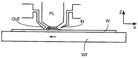
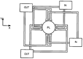
도 2 및 도 3은 리소그래피 투영 장치에서 사용하는 액체 공급 시스템을 도시하는 도면;
도 4는 리소그래피 투영 장치에서 사용하는 또 다른 액체 공급 시스템을 도시하는 도면;
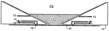
도 5는 침지 리소그래피 장치에서 사용하는 또 다른 액체 공급 시스템의 단면도;
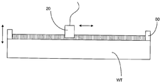
도 6은 기판 테이블을 클리닝하는 본 발명의 제 1 실시예의 단면도;
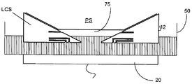
도 7은 액체 공급 시스템을 클리닝하는 본 발명의 제 2 실시예의 단면도; 및
도 8은 기판 테이블을 클리닝하는 본 발명의 제 3 실시예의 단면도이다.
Claims (15)
- 침지 리소그래피 투영 장치에 있어서:
기판을 유지하도록 구성되고 배치된 기판 테이블;
상기 기판 상에 방사선의 패터닝된 빔을 투영하도록 구성된 투영 시스템 - 상기 투영 시스템은 최종 요소를 가짐 - ;
표면을 클리닝(clean)하도록 구성된 메가소닉 트랜스듀서(megasonic transducer); 및
상기 메가소닉 트랜스듀서와 클리닝될 상기 표면 사이의 공간에 액체를 공급하도록 구성되고 배치되는 액체 공급 시스템
을 포함하여 이루어지고,
상기 최종 요소는 메가소닉 웨이브 및 클리닝 액체 중 적어도 어느 하나에 의한 손상으로부터 보호되는 것을 특징으로 하는 침지 리소그래피 투영 장치. - 제1항에 있어서,
상기 액체 공급 시스템은, 상기 투영 시스템의 최종 요소와 상기 기판 사이 내에 상기 기판의 국부화된 영역 상에만 액체를 공급하기 위한 액체 한정 구조체를 포함하는 것을 특징으로 하는 침지 리소그래피 투영 장치. - 제1항에 있어서,
상기 최종 요소는 실드(shield)에 의하여 메가소닉 웨이브 및 클리닝 액체 중 적어도 어느 하나에 의한 손상으로부터 보호되는 것을 특징으로 하는 침지 리소그래피 투영 장치. - 제3항에 있어서,
상기 실드는 플레이트를 포함하는 것을 특징으로 하는 침지 리소그래피 투영 장치. - 제2항에 있어서,
상기 액체의 수위(level)는, 상기 액체 한정 구조체의 저부 표면을 커버하고 상기 투영 시스템의 최종 요소는 커버하지 않도록 제어되는 것을 특징으로 하는 침지 리소그래피 투영 장치. - 제5항에 있어서,
상기 최종 요소와 액체로 채워지지 않는 상기 액체 수위 사이에는 간격(gap)이 존재하는 것을 특징으로 하는 침지 리소그래피 투영 장치. - 제2항 내지 제6항 중 어느 한 항에 있어서,
클리닝될 상기 표면은 상기 액체 한정 구조체의 하부인 것을 특징으로 하는 침지 리소그래피 투영 장치. - 제2항 내지 제6항 중 어느 한 항에 있어서,
상기 액체 한정 구조체는 방벽 부재(barrier member)를 포함하고, 상기 방벽 부재는 상기 메가소닉 트랜스듀서의 하단을 둘러싸고 상기 방벽 부재와 클리닝될 상기 표면 사이의 시일(seal)을 형성하고, 이로 인하여 상기 메가소닉 트랜스듀서와 클리닝될 상기 표면 사이의 액체를 유지(contain)하는 것을 특징으로 하는 침지 리소그래피 투영 장치. - 제8항에 있어서,
상기 방벽 부재, 상기 메가소닉 트랜스듀서, 또는 이들 모두는 상기 표면에 대하여 이동가능한 것을 특징으로 하는 침지 리소그래피 투영 장치. - 제9항에 있어서,
상기 표면은 상기 기판 테이블의 최상부 표면인 것을 특징으로 하는 침지 리소그래피 투영 장치. - 제1항 내지 제6항 중 어느 한 항에 있어서,
상기 액체 공급 시스템은 상기 표면 위로 액체 유동을 제공하도록 구성되고 배치되는 것을 특징으로 하는 침지 리소그래피 투영 장치. - 제1항 내지 제6항 중 어느 한 항에 있어서,
상기 메가소닉 트랜스듀서는, 클리닝 모드에서 메가소닉 웨이브들이 조준선(line of sight) 경로에서 클리닝될 상기 표면으로 지향되도록 상기 표면에 직면하여 위치되는 것을 특징으로 하는 침지 리소그래피 투영 장치. - 투영 시스템의 최종 요소를 포함하는 침지 리소그래피 투영 장치의 표면을 클리닝하는 방법에 있어서:
클리닝될 상기 표면의 적어도 일부분을 액체로 커버하는 단계;
상기 액체 내로 메가소닉 웨이브를 도입하는 단계; 및
상기 메가소닉 웨이브 및 클리닝 액체 중 적어도 어느 하나에 의한 손상으로부터 상기 최종 요소를 보호하는 단계를 포함하여 이루어지는 클리닝 방법. - 침지 리소그래피 투영 장치에 있어서:
기판을 유지하도록 구성되고 배치된 기판 테이블;
상기 기판 상에 방사선의 패터닝된 빔을 투영하도록 구성된 투영 시스템;
표면을 클리닝(clean)하도록 구성된 메가소닉 트랜스듀서(megasonic transducer); 및
상기 투영 시스템과 노광될 상기 기판 사이에 액체를 한정하도록 구성된 액체 한정 구조체
을 포함하여 이루어지고,
적어도 클리닝 모드에서, 메가소닉 웨이브 또는 액체 또는 둘 다로부터 상기 투영 시스템의 광학 요소를 실드하기 위하여 침지 액체와 투영 시스템의 저부면 사이에 실드(shield)가 제공되고, 상기 침지 액체는 '액체 한정 구조체', '투영 시스템', 및 '기판 및 기판 테이블 중 적어도 어느 하나'와의 사이에 정의된 공간에 있는 것을 특징으로 하는 침지 리소그래피 투영 장치. - 침지 리소그래피 투영 장치에 있어서:
기판을 유지하도록 구성되고 배치된 기판 테이블;
상기 기판 상에 방사선의 패터닝된 빔을 투영하도록 구성된 투영 시스템;
표면을 클리닝(clean)하도록 구성된 메가소닉 트랜스듀서(megasonic transducer); 및
상기 투영 시스템과 노광될 상기 기판 사이에 액체를 한정하도록 구성된 액체 한정 구조체
을 포함하여 이루어지고,
적어도 클리닝 모드에서, 메가소닉 웨이브 또는 액체 또는 둘 다로부터 상기 투영 시스템의 광학 요소를 보호하기 위하여 침지 액체와 투영 시스템의 저부면 사이에 간격(gap)이 제공되고, 상기 침지 액체는 '액체 한정 시스템', '투영 시스템', 및 '기판 및 기판 테이블 중 적어도 어느 하나'와의 사이에 정의된 공간에 있는 것을 특징으로 하는 침지 리소그래피 투영 장치.
Applications Claiming Priority (2)
| Application Number | Priority Date | Filing Date | Title |
|---|---|---|---|
| US11/437,876 US7969548B2 (en) | 2006-05-22 | 2006-05-22 | Lithographic apparatus and lithographic apparatus cleaning method |
| US11/437,876 | 2006-05-22 |
Related Parent Applications (1)
| Application Number | Title | Priority Date | Filing Date |
|---|---|---|---|
| KR1020080105320A Division KR101213594B1 (ko) | 2006-05-22 | 2008-10-27 | 리소그래피 장치 및 리소그래피 장치 클리닝 방법 |
Publications (1)
| Publication Number | Publication Date |
|---|---|
| KR20120052925A true KR20120052925A (ko) | 2012-05-24 |
Family
ID=38181126
Family Applications (3)
| Application Number | Title | Priority Date | Filing Date |
|---|---|---|---|
| KR1020070049369A Expired - Fee Related KR100897862B1 (ko) | 2006-05-22 | 2007-05-21 | 리소그래피 장치 및 리소그래피 장치 클리닝 방법 |
| KR1020080105320A Expired - Fee Related KR101213594B1 (ko) | 2006-05-22 | 2008-10-27 | 리소그래피 장치 및 리소그래피 장치 클리닝 방법 |
| KR1020120050989A Ceased KR20120052925A (ko) | 2006-05-22 | 2012-05-14 | 리소그래피 장치 및 리소그래피 장치 클리닝 방법 |
Family Applications Before (2)
| Application Number | Title | Priority Date | Filing Date |
|---|---|---|---|
| KR1020070049369A Expired - Fee Related KR100897862B1 (ko) | 2006-05-22 | 2007-05-21 | 리소그래피 장치 및 리소그래피 장치 클리닝 방법 |
| KR1020080105320A Expired - Fee Related KR101213594B1 (ko) | 2006-05-22 | 2008-10-27 | 리소그래피 장치 및 리소그래피 장치 클리닝 방법 |
Country Status (7)
| Country | Link |
|---|---|
| US (3) | US7969548B2 (ko) |
| EP (2) | EP1860507B1 (ko) |
| JP (3) | JP4691066B2 (ko) |
| KR (3) | KR100897862B1 (ko) |
| CN (2) | CN102081310A (ko) |
| SG (1) | SG137811A1 (ko) |
| TW (2) | TWI367401B (ko) |
Families Citing this family (48)
| Publication number | Priority date | Publication date | Assignee | Title |
|---|---|---|---|---|
| EP2261742A3 (en) | 2003-06-11 | 2011-05-25 | ASML Netherlands BV | Lithographic apparatus and device manufacturing method. |
| US7050146B2 (en) | 2004-02-09 | 2006-05-23 | Asml Netherlands B.V. | Lithographic apparatus and device manufacturing method |
| US7385670B2 (en) * | 2004-10-05 | 2008-06-10 | Asml Netherlands B.V. | Lithographic apparatus, cleaning system and cleaning method for in situ removing contamination from a component in a lithographic apparatus |
| WO2006062065A1 (ja) | 2004-12-06 | 2006-06-15 | Nikon Corporation | メンテナンス方法、メンテナンス機器、露光装置、及びデバイス製造方法 |
| US7880860B2 (en) | 2004-12-20 | 2011-02-01 | Asml Netherlands B.V. | Lithographic apparatus and device manufacturing method |
| TW200710616A (en) * | 2005-07-11 | 2007-03-16 | Nikon Corp | Exposure apparatus and method for manufacturing device |
| US8125610B2 (en) | 2005-12-02 | 2012-02-28 | ASML Metherlands B.V. | Method for preventing or reducing contamination of an immersion type projection apparatus and an immersion type lithographic apparatus |
| EP2037486A4 (en) * | 2006-05-18 | 2012-01-11 | Nikon Corp | EXPOSURE METHOD AND DEVICE, MAINTENANCE METHOD AND COMPONENT MANUFACTURING METHOD |
| TW200818256A (en) * | 2006-05-22 | 2008-04-16 | Nikon Corp | Exposure method and apparatus, maintenance method, and device manufacturing method |
| US7969548B2 (en) * | 2006-05-22 | 2011-06-28 | Asml Netherlands B.V. | Lithographic apparatus and lithographic apparatus cleaning method |
| EP2034515A4 (en) * | 2006-05-23 | 2012-01-18 | Nikon Corp | MAINTENANCE METHOD, EXPOSURE METHOD AND DEVICE AND COMPONENT MANUFACTURING METHOD |
| WO2008001871A1 (en) * | 2006-06-30 | 2008-01-03 | Nikon Corporation | Maintenance method, exposure method and apparatus and device manufacturing method |
| WO2008029884A1 (en) * | 2006-09-08 | 2008-03-13 | Nikon Corporation | Cleaning member, cleaning method and device manufacturing method |
| US20080156356A1 (en) * | 2006-12-05 | 2008-07-03 | Nikon Corporation | Cleaning liquid, cleaning method, liquid generating apparatus, exposure apparatus, and device fabricating method |
| US8654305B2 (en) | 2007-02-15 | 2014-02-18 | Asml Holding N.V. | Systems and methods for insitu lens cleaning in immersion lithography |
| US8817226B2 (en) | 2007-02-15 | 2014-08-26 | Asml Holding N.V. | Systems and methods for insitu lens cleaning using ozone in immersion lithography |
| JP2010519722A (ja) * | 2007-02-23 | 2010-06-03 | 株式会社ニコン | 露光方法、露光装置、デバイス製造方法、及び液浸露光用基板 |
| US7900641B2 (en) * | 2007-05-04 | 2011-03-08 | Asml Netherlands B.V. | Cleaning device and a lithographic apparatus cleaning method |
| US8947629B2 (en) | 2007-05-04 | 2015-02-03 | Asml Netherlands B.V. | Cleaning device, a lithographic apparatus and a lithographic apparatus cleaning method |
| US8011377B2 (en) * | 2007-05-04 | 2011-09-06 | Asml Netherlands B.V. | Cleaning device and a lithographic apparatus cleaning method |
| US7866330B2 (en) * | 2007-05-04 | 2011-01-11 | Asml Netherlands B.V. | Cleaning device, a lithographic apparatus and a lithographic apparatus cleaning method |
| US8098362B2 (en) * | 2007-05-30 | 2012-01-17 | Nikon Corporation | Detection device, movable body apparatus, pattern formation apparatus and pattern formation method, exposure apparatus and exposure method, and device manufacturing method |
| US7916269B2 (en) | 2007-07-24 | 2011-03-29 | Asml Netherlands B.V. | Lithographic apparatus and contamination removal or prevention method |
| US20090025753A1 (en) * | 2007-07-24 | 2009-01-29 | Asml Netherlands B.V. | Lithographic Apparatus And Contamination Removal Or Prevention Method |
| NL1035942A1 (nl) * | 2007-09-27 | 2009-03-30 | Asml Netherlands Bv | Lithographic Apparatus and Method of Cleaning a Lithographic Apparatus. |
| SG151198A1 (en) * | 2007-09-27 | 2009-04-30 | Asml Netherlands Bv | Methods relating to immersion lithography and an immersion lithographic apparatus |
| JP5017232B2 (ja) * | 2007-10-31 | 2012-09-05 | エーエスエムエル ネザーランズ ビー.ブイ. | クリーニング装置および液浸リソグラフィ装置 |
| NL1036273A1 (nl) * | 2007-12-18 | 2009-06-19 | Asml Netherlands Bv | Lithographic apparatus and method of cleaning a surface of an immersion lithographic apparatus. |
| NL1036306A1 (nl) | 2007-12-20 | 2009-06-23 | Asml Netherlands Bv | Lithographic apparatus and in-line cleaning apparatus. |
| KR101423611B1 (ko) * | 2008-01-16 | 2014-07-30 | 삼성전자주식회사 | 기판 처리 장치, 노광 장치 및 클리닝 툴의 세정 방법 |
| US8339572B2 (en) | 2008-01-25 | 2012-12-25 | Asml Netherlands B.V. | Lithographic apparatus and device manufacturing method |
| NL1036571A1 (nl) | 2008-03-07 | 2009-09-08 | Asml Netherlands Bv | Lithographic Apparatus and Methods. |
| KR101160948B1 (ko) | 2008-04-16 | 2012-06-28 | 에이에스엠엘 네델란즈 비.브이. | 리소그래피 장치 |
| US8619231B2 (en) * | 2009-05-21 | 2013-12-31 | Nikon Corporation | Cleaning method, exposure method, and device manufacturing method |
| NL2005610A (en) | 2009-12-02 | 2011-06-06 | Asml Netherlands Bv | Lithographic apparatus and surface cleaning method. |
| CA2784148A1 (en) * | 2009-12-28 | 2011-07-28 | Pioneer Hi-Bred International, Inc. | Sorghum fertility restorer genotypes and methods of marker-assisted selection |
| US20120160264A1 (en) * | 2010-12-23 | 2012-06-28 | Richard Endo | Wet Processing Tool with Site Isolation |
| US8974606B2 (en) | 2011-05-09 | 2015-03-10 | Intermolecular, Inc. | Ex-situ cleaning assembly |
| JP5893882B2 (ja) * | 2011-09-28 | 2016-03-23 | 東京エレクトロン株式会社 | パーティクル捕集装置及びパーティクルの捕集方法 |
| US9005366B2 (en) | 2011-10-06 | 2015-04-14 | Intermolecular, Inc. | In-situ reactor cleaning in high productivity combinatorial system |
| CN102629567B (zh) * | 2011-10-19 | 2015-06-24 | 京东方科技集团股份有限公司 | 一种基板固定装置及制作方法以及固定基板的方法 |
| TWI576657B (zh) * | 2014-12-25 | 2017-04-01 | 台灣積體電路製造股份有限公司 | 光罩清潔設備以及光罩清潔方法 |
| JP5963929B1 (ja) * | 2015-09-04 | 2016-08-03 | 株式会社日立パワーソリューションズ | 超音波検査装置、超音波検査システム、及び超音波検査方法 |
| US10256132B2 (en) * | 2016-04-28 | 2019-04-09 | Varian Semiconductor Equipment Associates, Inc. | Reticle processing system |
| CN107619098A (zh) * | 2016-08-19 | 2018-01-23 | Mag技术株式会社 | 碳酸氢气水及其在基板表面的应用 |
| CN109994372A (zh) * | 2019-04-15 | 2019-07-09 | 西安奕斯伟硅片技术有限公司 | 晶圆清洗方法及晶圆清洗装置 |
| CN110711739A (zh) * | 2019-09-29 | 2020-01-21 | 中国科学院长春光学精密机械与物理研究所 | 一种用于深紫外CaF2光学基底的清洗方法 |
| CN112871862A (zh) * | 2021-01-12 | 2021-06-01 | 佛山市南海区聚和超声波设备有限公司 | 一种线材超声波清洗装置 |
Family Cites Families (169)
| Publication number | Priority date | Publication date | Assignee | Title |
|---|---|---|---|---|
| GB1242527A (en) | 1967-10-20 | 1971-08-11 | Kodak Ltd | Optical instruments |
| US3573975A (en) | 1968-07-10 | 1971-04-06 | Ibm | Photochemical fabrication process |
| ATE1462T1 (de) | 1979-07-27 | 1982-08-15 | Werner W. Dr. Tabarelli | Optisches lithographieverfahren und einrichtung zum kopieren eines musters auf eine halbleiterscheibe. |
| FR2474708B1 (fr) | 1980-01-24 | 1987-02-20 | Dme | Procede de microphotolithographie a haute resolution de traits |
| JPS5754317A (en) | 1980-09-19 | 1982-03-31 | Hitachi Ltd | Method and device for forming pattern |
| US4509852A (en) | 1980-10-06 | 1985-04-09 | Werner Tabarelli | Apparatus for the photolithographic manufacture of integrated circuit elements |
| US4346164A (en) | 1980-10-06 | 1982-08-24 | Werner Tabarelli | Photolithographic method for the manufacture of integrated circuits |
| US4390273A (en) | 1981-02-17 | 1983-06-28 | Censor Patent-Und Versuchsanstalt | Projection mask as well as a method and apparatus for the embedding thereof and projection printing system |
| JPS57153433A (en) | 1981-03-18 | 1982-09-22 | Hitachi Ltd | Manufacturing device for semiconductor |
| US4405701A (en) | 1981-07-29 | 1983-09-20 | Western Electric Co. | Methods of fabricating a photomask |
| US5040020A (en) | 1988-03-31 | 1991-08-13 | Cornell Research Foundation, Inc. | Self-aligned, high resolution resonant dielectric lithography |
| JPH03209479A (ja) | 1989-09-06 | 1991-09-12 | Sanee Giken Kk | 露光方法 |
| US5143103A (en) * | 1991-01-04 | 1992-09-01 | International Business Machines Corporation | Apparatus for cleaning and drying workpieces |
| US5121256A (en) | 1991-03-14 | 1992-06-09 | The Board Of Trustees Of The Leland Stanford Junior University | Lithography system employing a solid immersion lens |
| JP2753930B2 (ja) | 1992-11-27 | 1998-05-20 | キヤノン株式会社 | 液浸式投影露光装置 |
| JPH08316124A (ja) | 1995-05-19 | 1996-11-29 | Hitachi Ltd | 投影露光方法及び露光装置 |
| JP3198899B2 (ja) | 1995-11-30 | 2001-08-13 | アルプス電気株式会社 | ウエット処理方法 |
| US6629640B2 (en) * | 1995-12-18 | 2003-10-07 | Metrologic Instruments, Inc. | Holographic laser scanning method and system employing visible scanning-zone indicators identifying a three-dimensional omni-directional laser scanning volume for package transport navigation |
| KR980012021A (ko) * | 1996-07-29 | 1998-04-30 | 김광호 | 반도체 소자의 세정방법 |
| US6104687A (en) | 1996-08-26 | 2000-08-15 | Digital Papyrus Corporation | Method and apparatus for coupling an optical lens to a disk through a coupling medium having a relatively high index of refraction |
| US5825043A (en) | 1996-10-07 | 1998-10-20 | Nikon Precision Inc. | Focusing and tilting adjustment system for lithography aligner, manufacturing apparatus or inspection apparatus |
| JPH1133506A (ja) * | 1997-07-24 | 1999-02-09 | Tadahiro Omi | 流体処理装置及び洗浄処理システム |
| US5900354A (en) | 1997-07-03 | 1999-05-04 | Batchelder; John Samuel | Method for optical inspection and lithography |
| JPH11162831A (ja) * | 1997-11-21 | 1999-06-18 | Nikon Corp | 投影露光装置及び投影露光方法 |
| WO1999027568A1 (en) | 1997-11-21 | 1999-06-03 | Nikon Corporation | Projection aligner and projection exposure method |
| JPH11176727A (ja) * | 1997-12-11 | 1999-07-02 | Nikon Corp | 投影露光装置 |
| EP1039511A4 (en) | 1997-12-12 | 2005-03-02 | Nikon Corp | PROJECTION EXPOSURE PROCESSING METHOD AND PROJECTION APPARATUS |
| US5837662A (en) | 1997-12-12 | 1998-11-17 | Memc Electronic Materials, Inc. | Post-lapping cleaning process for silicon wafers |
| JP2000058436A (ja) | 1998-08-11 | 2000-02-25 | Nikon Corp | 投影露光装置及び露光方法 |
| TWI242111B (en) | 1999-04-19 | 2005-10-21 | Asml Netherlands Bv | Gas bearings for use in vacuum chambers and their application in lithographic projection apparatus |
| JP2000323396A (ja) | 1999-05-13 | 2000-11-24 | Canon Inc | 露光方法、露光装置、およびデイバイス製造方法 |
| JP4504479B2 (ja) | 1999-09-21 | 2010-07-14 | オリンパス株式会社 | 顕微鏡用液浸対物レンズ |
| US6743301B2 (en) | 1999-12-24 | 2004-06-01 | mFSI Ltd. | Substrate treatment process and apparatus |
| US6523210B1 (en) * | 2000-04-05 | 2003-02-25 | Nicholas Andros | Surface charge controlling apparatus for wafer cleaning |
| US6539952B2 (en) * | 2000-04-25 | 2003-04-01 | Solid State Equipment Corp. | Megasonic treatment apparatus |
| US6927176B2 (en) * | 2000-06-26 | 2005-08-09 | Applied Materials, Inc. | Cleaning method and solution for cleaning a wafer in a single wafer process |
| TW591653B (en) | 2000-08-08 | 2004-06-11 | Koninkl Philips Electronics Nv | Method of manufacturing an optically scannable information carrier |
| JP2002075947A (ja) * | 2000-08-30 | 2002-03-15 | Alps Electric Co Ltd | ウェット処理装置 |
| WO2002091078A1 (en) | 2001-05-07 | 2002-11-14 | Massachusetts Institute Of Technology | Methods and apparatus employing an index matching medium |
| US6600547B2 (en) | 2001-09-24 | 2003-07-29 | Nikon Corporation | Sliding seal |
| EP1446703A2 (en) | 2001-11-07 | 2004-08-18 | Applied Materials, Inc. | Optical spot grid array printer |
| US6955485B2 (en) | 2002-03-01 | 2005-10-18 | Tokyo Electron Limited | Developing method and developing unit |
| DE10229818A1 (de) | 2002-06-28 | 2004-01-15 | Carl Zeiss Smt Ag | Verfahren zur Fokusdetektion und Abbildungssystem mit Fokusdetektionssystem |
| US7198055B2 (en) * | 2002-09-30 | 2007-04-03 | Lam Research Corporation | Meniscus, vacuum, IPA vapor, drying manifold |
| US8236382B2 (en) | 2002-09-30 | 2012-08-07 | Lam Research Corporation | Proximity substrate preparation sequence, and method, apparatus, and system for implementing the same |
| US6788477B2 (en) | 2002-10-22 | 2004-09-07 | Taiwan Semiconductor Manufacturing Co., Ltd. | Apparatus for method for immersion lithography |
| SG121819A1 (en) | 2002-11-12 | 2006-05-26 | Asml Netherlands Bv | Lithographic apparatus and device manufacturing method |
| EP1420300B1 (en) | 2002-11-12 | 2015-07-29 | ASML Netherlands B.V. | Lithographic apparatus and device manufacturing method |
| CN101382738B (zh) | 2002-11-12 | 2011-01-12 | Asml荷兰有限公司 | 光刻投射装置 |
| KR100585476B1 (ko) | 2002-11-12 | 2006-06-07 | 에이에스엠엘 네델란즈 비.브이. | 리소그래피 장치 및 디바이스 제조방법 |
| DE60335595D1 (de) | 2002-11-12 | 2011-02-17 | Asml Netherlands Bv | Lithographischer Apparat mit Immersion und Verfahren zur Herstellung einer Vorrichtung |
| SG121822A1 (en) | 2002-11-12 | 2006-05-26 | Asml Netherlands Bv | Lithographic apparatus and device manufacturing method |
| SG131766A1 (en) | 2002-11-18 | 2007-05-28 | Asml Netherlands Bv | Lithographic apparatus and device manufacturing method |
| WO2004050266A1 (ja) | 2002-12-03 | 2004-06-17 | Nikon Corporation | 汚染物質除去方法及び装置、並びに露光方法及び装置 |
| AU2003289272A1 (en) | 2002-12-10 | 2004-06-30 | Nikon Corporation | Surface position detection apparatus, exposure method, and device porducing method |
| SG171468A1 (en) | 2002-12-10 | 2011-06-29 | Nikon Corp | Exposure apparatus and method for producing device |
| KR101157002B1 (ko) | 2002-12-10 | 2012-06-21 | 가부시키가이샤 니콘 | 노광 장치 및 디바이스 제조 방법 |
| EP1571700A4 (en) | 2002-12-10 | 2007-09-12 | Nikon Corp | OPTICAL DEVICE AND PROJECTION EXPOSURE DEVICE USING THE OPTICAL DEVICE |
| US7242455B2 (en) | 2002-12-10 | 2007-07-10 | Nikon Corporation | Exposure apparatus and method for producing device |
| DE10257766A1 (de) | 2002-12-10 | 2004-07-15 | Carl Zeiss Smt Ag | Verfahren zur Einstellung einer gewünschten optischen Eigenschaft eines Projektionsobjektivs sowie mikrolithografische Projektionsbelichtungsanlage |
| EP1571701A4 (en) | 2002-12-10 | 2008-04-09 | Nikon Corp | EXPOSURE DEVICE AND METHOD FOR MANUFACTURING COMPONENTS |
| AU2003289271A1 (en) | 2002-12-10 | 2004-06-30 | Nikon Corporation | Exposure apparatus, exposure method and method for manufacturing device |
| CN101872135B (zh) | 2002-12-10 | 2013-07-31 | 株式会社尼康 | 曝光设备和器件制造法 |
| EP1571695A4 (en) | 2002-12-10 | 2008-10-15 | Nikon Corp | EXPOSURE DEVICE AND METHOD FOR PRODUCING THE DEVICE |
| JP4232449B2 (ja) | 2002-12-10 | 2009-03-04 | 株式会社ニコン | 露光方法、露光装置、及びデバイス製造方法 |
| EP1429190B1 (en) | 2002-12-10 | 2012-05-09 | Canon Kabushiki Kaisha | Exposure apparatus and method |
| JP4352874B2 (ja) | 2002-12-10 | 2009-10-28 | 株式会社ニコン | 露光装置及びデバイス製造方法 |
| AU2003302831A1 (en) | 2002-12-10 | 2004-06-30 | Nikon Corporation | Exposure method, exposure apparatus and method for manufacturing device |
| ATE424026T1 (de) | 2002-12-13 | 2009-03-15 | Koninkl Philips Electronics Nv | Flüssigkeitsentfernung in einem verfahren und einer einrichtung zum bestrahlen von flecken auf einer schicht |
| EP1429189B1 (en) * | 2002-12-13 | 2008-10-08 | ASML Netherlands B.V. | Lithographic apparatus and device manufacturing method |
| USRE48515E1 (en) | 2002-12-19 | 2021-04-13 | Asml Netherlands B.V. | Method and device for irradiating spots on a layer |
| EP1732075A3 (en) | 2002-12-19 | 2007-02-21 | Koninklijke Philips Electronics N.V. | Method and device for irradiating spots on a layer |
| US6781670B2 (en) | 2002-12-30 | 2004-08-24 | Intel Corporation | Immersion lithography |
| KR20170016014A (ko) * | 2003-04-11 | 2017-02-10 | 가부시키가이샤 니콘 | 액침 리소그래피에 의한 광학기기의 세정방법 |
| TWI295414B (en) | 2003-05-13 | 2008-04-01 | Asml Netherlands Bv | Lithographic apparatus and device manufacturing method |
| TWI424470B (zh) | 2003-05-23 | 2014-01-21 | 尼康股份有限公司 | A method of manufacturing an exposure apparatus and an element |
| US7274472B2 (en) | 2003-05-28 | 2007-09-25 | Timbre Technologies, Inc. | Resolution enhanced optical metrology |
| DE10324477A1 (de) * | 2003-05-30 | 2004-12-30 | Carl Zeiss Smt Ag | Mikrolithographische Projektionsbelichtungsanlage |
| EP2261742A3 (en) * | 2003-06-11 | 2011-05-25 | ASML Netherlands BV | Lithographic apparatus and device manufacturing method. |
| JP4643582B2 (ja) * | 2003-06-11 | 2011-03-02 | アクリオン テクノロジーズ インク | 過飽和の洗浄溶液を使用したメガソニック洗浄 |
| JP2005019616A (ja) | 2003-06-25 | 2005-01-20 | Canon Inc | 液浸式露光装置 |
| JP4343597B2 (ja) | 2003-06-25 | 2009-10-14 | キヤノン株式会社 | 露光装置及びデバイス製造方法 |
| EP1498778A1 (en) | 2003-06-27 | 2005-01-19 | ASML Netherlands B.V. | Lithographic apparatus and device manufacturing method |
| JP3862678B2 (ja) | 2003-06-27 | 2006-12-27 | キヤノン株式会社 | 露光装置及びデバイス製造方法 |
| SG109000A1 (en) | 2003-07-16 | 2005-02-28 | Asml Netherlands Bv | Lithographic apparatus and device manufacturing method |
| US7370659B2 (en) * | 2003-08-06 | 2008-05-13 | Micron Technology, Inc. | Photolithographic stepper and/or scanner machines including cleaning devices and methods of cleaning photolithographic stepper and/or scanner machines |
| JP2005072404A (ja) | 2003-08-27 | 2005-03-17 | Sony Corp | 露光装置および半導体装置の製造方法 |
| JP4305095B2 (ja) | 2003-08-29 | 2009-07-29 | 株式会社ニコン | 光学部品の洗浄機構を搭載した液浸投影露光装置及び液浸光学部品洗浄方法 |
| US7070915B2 (en) | 2003-08-29 | 2006-07-04 | Tokyo Electron Limited | Method and system for drying a substrate |
| US6954256B2 (en) | 2003-08-29 | 2005-10-11 | Asml Netherlands B.V. | Gradient immersion lithography |
| US7014966B2 (en) | 2003-09-02 | 2006-03-21 | Advanced Micro Devices, Inc. | Method and apparatus for elimination of bubbles in immersion medium in immersion lithography systems |
| JP4378136B2 (ja) | 2003-09-04 | 2009-12-02 | キヤノン株式会社 | 露光装置及びデバイス製造方法 |
| JP3870182B2 (ja) | 2003-09-09 | 2007-01-17 | キヤノン株式会社 | 露光装置及びデバイス製造方法 |
| KR101248325B1 (ko) * | 2003-09-26 | 2013-03-27 | 가부시키가이샤 니콘 | 투영노광장치 및 투영노광장치의 세정방법, 메인터넌스방법 그리고 디바이스의 제조방법 |
| CN1860585B (zh) * | 2003-09-29 | 2010-04-28 | 株式会社尼康 | 液浸型透镜系统和投影曝光装置 |
| JP4513299B2 (ja) * | 2003-10-02 | 2010-07-28 | 株式会社ニコン | 露光装置、露光方法、及びデバイス製造方法 |
| EP1672682A4 (en) | 2003-10-08 | 2008-10-15 | Zao Nikon Co Ltd | SUBSTRATE TRANSPORT DEVICE AND METHOD, EXPOSURE DEVICE AND METHOD AND COMPONENT MANUFACTURING METHOD |
| EP1524558A1 (en) * | 2003-10-15 | 2005-04-20 | ASML Netherlands B.V. | Lithographic apparatus and device manufacturing method |
| JP2005159322A (ja) | 2003-10-31 | 2005-06-16 | Nikon Corp | 定盤、ステージ装置及び露光装置並びに露光方法 |
| US7528929B2 (en) | 2003-11-14 | 2009-05-05 | Asml Netherlands B.V. | Lithographic apparatus and device manufacturing method |
| JP2005175016A (ja) | 2003-12-08 | 2005-06-30 | Canon Inc | 基板保持装置およびそれを用いた露光装置ならびにデバイス製造方法 |
| JP2005175034A (ja) | 2003-12-09 | 2005-06-30 | Canon Inc | 露光装置 |
| US7458226B2 (en) | 2003-12-18 | 2008-12-02 | Calsonic Kansei Corporation | Air conditioning system, vehicular air conditioning system and control method of vehicular air conditioning system |
| US7460206B2 (en) * | 2003-12-19 | 2008-12-02 | Carl Zeiss Smt Ag | Projection objective for immersion lithography |
| DE602004028511D1 (de) | 2003-12-23 | 2010-09-16 | Koninkl Philips Electronics Nv | Bestrahlungsverfahren |
| US7589818B2 (en) | 2003-12-23 | 2009-09-15 | Asml Netherlands B.V. | Lithographic apparatus, alignment apparatus, device manufacturing method, and a method of converting an apparatus |
| JP2005191381A (ja) | 2003-12-26 | 2005-07-14 | Canon Inc | 露光方法及び装置 |
| JP2005191393A (ja) | 2003-12-26 | 2005-07-14 | Canon Inc | 露光方法及び装置 |
| JP4429023B2 (ja) | 2004-01-07 | 2010-03-10 | キヤノン株式会社 | 露光装置及びデバイス製造方法 |
| JP4018647B2 (ja) | 2004-02-09 | 2007-12-05 | キヤノン株式会社 | 投影露光装置およびデバイス製造方法 |
| US7050146B2 (en) | 2004-02-09 | 2006-05-23 | Asml Netherlands B.V. | Lithographic apparatus and device manufacturing method |
| KR101166007B1 (ko) | 2004-02-10 | 2012-07-17 | 가부시키가이샤 니콘 | 노광 장치 및 디바이스 제조 방법, 메인터넌스 방법 및노광 방법 |
| JP4513590B2 (ja) * | 2004-02-19 | 2010-07-28 | 株式会社ニコン | 光学部品及び露光装置 |
| JP2005286068A (ja) | 2004-03-29 | 2005-10-13 | Canon Inc | 露光装置及び方法 |
| JP4510494B2 (ja) | 2004-03-29 | 2010-07-21 | キヤノン株式会社 | 露光装置 |
| US7091502B2 (en) | 2004-05-12 | 2006-08-15 | Taiwan Semiconductor Manufacturing, Co., Ltd. | Apparatus and method for immersion lithography |
| JP4655763B2 (ja) * | 2004-06-04 | 2011-03-23 | 株式会社ニコン | 露光装置、露光方法及びデバイス製造方法 |
| US8698998B2 (en) | 2004-06-21 | 2014-04-15 | Nikon Corporation | Exposure apparatus, method for cleaning member thereof, maintenance method for exposure apparatus, maintenance device, and method for producing device |
| EP3098835B1 (en) | 2004-06-21 | 2017-07-26 | Nikon Corporation | Exposure apparatus, exposure method and device manufacturing method |
| JP4677833B2 (ja) * | 2004-06-21 | 2011-04-27 | 株式会社ニコン | 露光装置、及びその部材の洗浄方法、露光装置のメンテナンス方法、メンテナンス機器、並びにデバイス製造方法 |
| DE102004033208B4 (de) | 2004-07-09 | 2010-04-01 | Vistec Semiconductor Systems Gmbh | Vorrichtung zur Inspektion eines mikroskopischen Bauteils mit einem Immersionsobjektiv |
| US7307263B2 (en) | 2004-07-14 | 2007-12-11 | Asml Netherlands B.V. | Lithographic apparatus, radiation system, contaminant trap, device manufacturing method, and method for trapping contaminants in a contaminant trap |
| EP1801852A4 (en) * | 2004-07-16 | 2008-04-09 | Nikon Corp | CARRIER METHOD AND SUPPORT STRUCTURE FOR OPTICAL ELEMENTS, OPTICAL DEVICE, EXPOSURE DEVICE AND DEVICE MANUFACTURING METHOD |
| JP2006032750A (ja) * | 2004-07-20 | 2006-02-02 | Canon Inc | 液浸型投影露光装置、及びデバイス製造方法 |
| US7224427B2 (en) | 2004-08-03 | 2007-05-29 | Taiwan Semiconductor Manufacturing Company, Ltd. | Megasonic immersion lithography exposure apparatus and method |
| JP4772306B2 (ja) | 2004-09-06 | 2011-09-14 | 株式会社東芝 | 液浸光学装置及び洗浄方法 |
| US7385670B2 (en) | 2004-10-05 | 2008-06-10 | Asml Netherlands B.V. | Lithographic apparatus, cleaning system and cleaning method for in situ removing contamination from a component in a lithographic apparatus |
| JP2006120674A (ja) | 2004-10-19 | 2006-05-11 | Canon Inc | 露光装置及び方法、デバイス製造方法 |
| US7156925B1 (en) * | 2004-11-01 | 2007-01-02 | Advanced Micro Devices, Inc. | Using supercritical fluids to clean lenses and monitor defects |
| JP2006134999A (ja) | 2004-11-04 | 2006-05-25 | Sony Corp | 液浸型露光装置、及び、液浸型露光装置における保持台の洗浄方法 |
| US7362412B2 (en) * | 2004-11-18 | 2008-04-22 | International Business Machines Corporation | Method and apparatus for cleaning a semiconductor substrate in an immersion lithography system |
| EP1814146A4 (en) * | 2004-11-19 | 2009-02-11 | Nikon Corp | MAINTENANCE METHOD, EXPOSURE METHOD, EXPOSURE DEVICE AND COMPONENT MANUFACTURING METHOD |
| WO2006062065A1 (ja) * | 2004-12-06 | 2006-06-15 | Nikon Corporation | メンテナンス方法、メンテナンス機器、露光装置、及びデバイス製造方法 |
| US7880860B2 (en) | 2004-12-20 | 2011-02-01 | Asml Netherlands B.V. | Lithographic apparatus and device manufacturing method |
| JP2006261606A (ja) * | 2005-03-18 | 2006-09-28 | Canon Inc | 露光装置、露光方法及びデバイス製造方法 |
| JP2006310706A (ja) | 2005-05-02 | 2006-11-09 | Nikon Corp | 光学部品の洗浄方法、液浸投影露光装置および露光方法 |
| US20060250588A1 (en) | 2005-05-03 | 2006-11-09 | Stefan Brandl | Immersion exposure tool cleaning system and method |
| US7315033B1 (en) | 2005-05-04 | 2008-01-01 | Advanced Micro Devices, Inc. | Method and apparatus for reducing biological contamination in an immersion lithography system |
| US20070085989A1 (en) | 2005-06-21 | 2007-04-19 | Nikon Corporation | Exposure apparatus and exposure method, maintenance method, and device manufacturing method |
| US20070002296A1 (en) | 2005-06-30 | 2007-01-04 | Taiwan Semiconductor Manufacturing Company, Ltd. | Immersion lithography defect reduction |
| US7262422B2 (en) | 2005-07-01 | 2007-08-28 | Spansion Llc | Use of supercritical fluid to dry wafer and clean lens in immersion lithography |
| JP2007029973A (ja) | 2005-07-25 | 2007-02-08 | Sony Corp | レーザ加工装置とその加工方法及びデブリ回収装置とその回収方法 |
| JP2007088328A (ja) | 2005-09-26 | 2007-04-05 | Toshiba Corp | 液浸型露光装置の洗浄方法 |
| JP2007103658A (ja) | 2005-10-04 | 2007-04-19 | Canon Inc | 露光方法および装置ならびにデバイス製造方法 |
| US7986395B2 (en) | 2005-10-24 | 2011-07-26 | Taiwan Semiconductor Manufacturing Company, Ltd. | Immersion lithography apparatus and methods |
| CN1963673A (zh) | 2005-11-11 | 2007-05-16 | 台湾积体电路制造股份有限公司 | 浸润式微影曝光设备及方法 |
| JP2007142217A (ja) | 2005-11-18 | 2007-06-07 | Taiwan Semiconductor Manufacturing Co Ltd | イマージョン式リソグラフィ露光装置およびその方法 |
| JP2007150102A (ja) | 2005-11-29 | 2007-06-14 | Fujitsu Ltd | 露光装置及び光学素子の洗浄方法 |
| US8125610B2 (en) | 2005-12-02 | 2012-02-28 | ASML Metherlands B.V. | Method for preventing or reducing contamination of an immersion type projection apparatus and an immersion type lithographic apparatus |
| US7462850B2 (en) | 2005-12-08 | 2008-12-09 | Asml Netherlands B.V. | Radical cleaning arrangement for a lithographic apparatus |
| US7405417B2 (en) | 2005-12-20 | 2008-07-29 | Asml Netherlands B.V. | Lithographic apparatus having a monitoring device for detecting contamination |
| US7522263B2 (en) | 2005-12-27 | 2009-04-21 | Asml Netherlands B.V. | Lithographic apparatus and method |
| US20070146658A1 (en) | 2005-12-27 | 2007-06-28 | Asml Netherlands B.V. | Lithographic apparatus and method |
| JP4704221B2 (ja) | 2006-01-26 | 2011-06-15 | 株式会社Sokudo | 基板処理装置および基板処理方法 |
| JP2007227543A (ja) | 2006-02-22 | 2007-09-06 | Toshiba Corp | 液浸光学装置、洗浄方法及び液浸露光方法 |
| JP2007227580A (ja) | 2006-02-23 | 2007-09-06 | Sony Corp | 液浸型露光装置および液浸型露光方法 |
| EP1995768A4 (en) * | 2006-03-13 | 2013-02-06 | Nikon Corp | EXPOSURE DEVICE, MAINTENANCE METHOD, EXPOSURE METHOD AND DEVICE MANUFACTURING METHOD |
| JP2007266074A (ja) | 2006-03-27 | 2007-10-11 | Toshiba Corp | 半導体装置の製造方法及び液浸リソグラフィーシステム |
| JP2007294817A (ja) | 2006-04-27 | 2007-11-08 | Sokudo:Kk | 基板処理方法、基板処理システムおよび基板処理装置 |
| US7628865B2 (en) | 2006-04-28 | 2009-12-08 | Asml Netherlands B.V. | Methods to clean a surface, a device manufacturing method, a cleaning assembly, cleaning apparatus, and lithographic apparatus |
| EP2037486A4 (en) * | 2006-05-18 | 2012-01-11 | Nikon Corp | EXPOSURE METHOD AND DEVICE, MAINTENANCE METHOD AND COMPONENT MANUFACTURING METHOD |
| US7969548B2 (en) | 2006-05-22 | 2011-06-28 | Asml Netherlands B.V. | Lithographic apparatus and lithographic apparatus cleaning method |
| EP2034515A4 (en) * | 2006-05-23 | 2012-01-18 | Nikon Corp | MAINTENANCE METHOD, EXPOSURE METHOD AND DEVICE AND COMPONENT MANUFACTURING METHOD |
| JP2007317987A (ja) | 2006-05-29 | 2007-12-06 | Sokudo:Kk | 基板処理装置および基板処理方法 |
| US8947629B2 (en) | 2007-05-04 | 2015-02-03 | Asml Netherlands B.V. | Cleaning device, a lithographic apparatus and a lithographic apparatus cleaning method |
| US7900641B2 (en) * | 2007-05-04 | 2011-03-08 | Asml Netherlands B.V. | Cleaning device and a lithographic apparatus cleaning method |
| US7916269B2 (en) | 2007-07-24 | 2011-03-29 | Asml Netherlands B.V. | Lithographic apparatus and contamination removal or prevention method |
| US20090025753A1 (en) | 2007-07-24 | 2009-01-29 | Asml Netherlands B.V. | Lithographic Apparatus And Contamination Removal Or Prevention Method |
| NL2005610A (en) * | 2009-12-02 | 2011-06-06 | Asml Netherlands Bv | Lithographic apparatus and surface cleaning method. |
-
2006
- 2006-05-22 US US11/437,876 patent/US7969548B2/en not_active Expired - Fee Related
-
2007
- 2007-05-09 EP EP07251915A patent/EP1860507B1/en not_active Ceased
- 2007-05-09 EP EP11164878A patent/EP2365391A3/en not_active Withdrawn
- 2007-05-15 JP JP2007129288A patent/JP4691066B2/ja not_active Expired - Fee Related
- 2007-05-16 TW TW096117452A patent/TWI367401B/zh not_active IP Right Cessation
- 2007-05-16 TW TW101116087A patent/TW201243518A/zh unknown
- 2007-05-18 US US11/802,082 patent/US20080049201A1/en not_active Abandoned
- 2007-05-21 CN CN2010105591137A patent/CN102081310A/zh active Pending
- 2007-05-21 KR KR1020070049369A patent/KR100897862B1/ko not_active Expired - Fee Related
- 2007-05-21 CN CN2007101092015A patent/CN101078887B/zh active Active
- 2007-05-21 SG SG200703684-1A patent/SG137811A1/en unknown
-
2008
- 2008-10-27 KR KR1020080105320A patent/KR101213594B1/ko not_active Expired - Fee Related
-
2010
- 2010-11-22 JP JP2010260034A patent/JP2011071535A/ja active Pending
-
2011
- 2011-02-18 JP JP2011033186A patent/JP2011129951A/ja active Pending
- 2011-05-18 US US13/110,674 patent/US20110222034A1/en not_active Abandoned
-
2012
- 2012-05-14 KR KR1020120050989A patent/KR20120052925A/ko not_active Ceased
Also Published As
| Publication number | Publication date |
|---|---|
| EP1860507A1 (en) | 2007-11-28 |
| US20110222034A1 (en) | 2011-09-15 |
| US20080049201A1 (en) | 2008-02-28 |
| CN101078887A (zh) | 2007-11-28 |
| US20070285631A1 (en) | 2007-12-13 |
| KR20080108930A (ko) | 2008-12-16 |
| CN101078887B (zh) | 2012-07-25 |
| TWI367401B (en) | 2012-07-01 |
| CN102081310A (zh) | 2011-06-01 |
| TW200807169A (en) | 2008-02-01 |
| EP2365391A3 (en) | 2012-08-29 |
| SG137811A1 (en) | 2007-12-28 |
| EP2365391A2 (en) | 2011-09-14 |
| US7969548B2 (en) | 2011-06-28 |
| KR20070112726A (ko) | 2007-11-27 |
| TW201243518A (en) | 2012-11-01 |
| JP4691066B2 (ja) | 2011-06-01 |
| JP2011071535A (ja) | 2011-04-07 |
| EP1860507B1 (en) | 2011-08-17 |
| JP2007318129A (ja) | 2007-12-06 |
| KR101213594B1 (ko) | 2012-12-18 |
| JP2011129951A (ja) | 2011-06-30 |
| KR100897862B1 (ko) | 2009-05-18 |
Similar Documents
| Publication | Publication Date | Title |
|---|---|---|
| KR101213594B1 (ko) | 리소그래피 장치 및 리소그래피 장치 클리닝 방법 | |
| US7841352B2 (en) | Cleaning device, a lithographic apparatus and a lithographic apparatus cleaning method | |
| US8947629B2 (en) | Cleaning device, a lithographic apparatus and a lithographic apparatus cleaning method | |
| JP4939504B2 (ja) | リソグラフィ装置およびリソグラフィ装置を清浄する方法 | |
| US7866330B2 (en) | Cleaning device, a lithographic apparatus and a lithographic apparatus cleaning method | |
| US20110292359A1 (en) | Cleaning device and a lithographic apparatus cleaning method |
Legal Events
| Date | Code | Title | Description |
|---|---|---|---|
| A107 | Divisional application of patent | ||
| A201 | Request for examination | ||
| PA0107 | Divisional application |
St.27 status event code: A-0-1-A10-A18-div-PA0107 St.27 status event code: A-0-1-A10-A16-div-PA0107 |
|
| PA0201 | Request for examination |
St.27 status event code: A-1-2-D10-D11-exm-PA0201 |
|
| PG1501 | Laying open of application |
St.27 status event code: A-1-1-Q10-Q12-nap-PG1501 |
|
| E902 | Notification of reason for refusal | ||
| PE0902 | Notice of grounds for rejection |
St.27 status event code: A-1-2-D10-D21-exm-PE0902 |
|
| T11-X000 | Administrative time limit extension requested |
St.27 status event code: U-3-3-T10-T11-oth-X000 |
|
| T11-X000 | Administrative time limit extension requested |
St.27 status event code: U-3-3-T10-T11-oth-X000 |
|
| T11-X000 | Administrative time limit extension requested |
St.27 status event code: U-3-3-T10-T11-oth-X000 |
|
| T11-X000 | Administrative time limit extension requested |
St.27 status event code: U-3-3-T10-T11-oth-X000 |
|
| E601 | Decision to refuse application | ||
| PE0601 | Decision on rejection of patent |
St.27 status event code: N-2-6-B10-B15-exm-PE0601 |
|
| R18-X000 | Changes to party contact information recorded |
St.27 status event code: A-3-3-R10-R18-oth-X000 |
|
| P22-X000 | Classification modified |
St.27 status event code: A-2-2-P10-P22-nap-X000 |