KR20120122432A - 반사형 액정 디스플레이 장치 및 그 제조방법 - Google Patents
반사형 액정 디스플레이 장치 및 그 제조방법 Download PDFInfo
- Publication number
- KR20120122432A KR20120122432A KR1020110040562A KR20110040562A KR20120122432A KR 20120122432 A KR20120122432 A KR 20120122432A KR 1020110040562 A KR1020110040562 A KR 1020110040562A KR 20110040562 A KR20110040562 A KR 20110040562A KR 20120122432 A KR20120122432 A KR 20120122432A
- Authority
- KR
- South Korea
- Prior art keywords
- liquid crystal
- crystal panel
- color
- crystal material
- electrode
- Prior art date
- Legal status (The legal status is an assumption and is not a legal conclusion. Google has not performed a legal analysis and makes no representation as to the accuracy of the status listed.)
- Ceased
Links
Images





Classifications
-
- G—PHYSICS
- G02—OPTICS
- G02F—OPTICAL DEVICES OR ARRANGEMENTS FOR THE CONTROL OF LIGHT BY MODIFICATION OF THE OPTICAL PROPERTIES OF THE MEDIA OF THE ELEMENTS INVOLVED THEREIN; NON-LINEAR OPTICS; FREQUENCY-CHANGING OF LIGHT; OPTICAL LOGIC ELEMENTS; OPTICAL ANALOGUE/DIGITAL CONVERTERS
- G02F1/00—Devices or arrangements for the control of the intensity, colour, phase, polarisation or direction of light arriving from an independent light source, e.g. switching, gating or modulating; Non-linear optics
- G02F1/01—Devices or arrangements for the control of the intensity, colour, phase, polarisation or direction of light arriving from an independent light source, e.g. switching, gating or modulating; Non-linear optics for the control of the intensity, phase, polarisation or colour
- G02F1/13—Devices or arrangements for the control of the intensity, colour, phase, polarisation or direction of light arriving from an independent light source, e.g. switching, gating or modulating; Non-linear optics for the control of the intensity, phase, polarisation or colour based on liquid crystals, e.g. single liquid crystal display cells
- G02F1/133—Constructional arrangements; Operation of liquid crystal cells; Circuit arrangements
- G02F1/1333—Constructional arrangements; Manufacturing methods
- G02F1/1347—Arrangement of liquid crystal layers or cells in which the final condition of one light beam is achieved by the addition of the effects of two or more layers or cells
- G02F1/13476—Arrangement of liquid crystal layers or cells in which the final condition of one light beam is achieved by the addition of the effects of two or more layers or cells in which at least one liquid crystal cell or layer assumes a scattering state
-
- G—PHYSICS
- G02—OPTICS
- G02F—OPTICAL DEVICES OR ARRANGEMENTS FOR THE CONTROL OF LIGHT BY MODIFICATION OF THE OPTICAL PROPERTIES OF THE MEDIA OF THE ELEMENTS INVOLVED THEREIN; NON-LINEAR OPTICS; FREQUENCY-CHANGING OF LIGHT; OPTICAL LOGIC ELEMENTS; OPTICAL ANALOGUE/DIGITAL CONVERTERS
- G02F1/00—Devices or arrangements for the control of the intensity, colour, phase, polarisation or direction of light arriving from an independent light source, e.g. switching, gating or modulating; Non-linear optics
- G02F1/01—Devices or arrangements for the control of the intensity, colour, phase, polarisation or direction of light arriving from an independent light source, e.g. switching, gating or modulating; Non-linear optics for the control of the intensity, phase, polarisation or colour
- G02F1/13—Devices or arrangements for the control of the intensity, colour, phase, polarisation or direction of light arriving from an independent light source, e.g. switching, gating or modulating; Non-linear optics for the control of the intensity, phase, polarisation or colour based on liquid crystals, e.g. single liquid crystal display cells
- G02F1/133—Constructional arrangements; Operation of liquid crystal cells; Circuit arrangements
- G02F1/1333—Constructional arrangements; Manufacturing methods
- G02F1/1347—Arrangement of liquid crystal layers or cells in which the final condition of one light beam is achieved by the addition of the effects of two or more layers or cells
-
- G—PHYSICS
- G02—OPTICS
- G02F—OPTICAL DEVICES OR ARRANGEMENTS FOR THE CONTROL OF LIGHT BY MODIFICATION OF THE OPTICAL PROPERTIES OF THE MEDIA OF THE ELEMENTS INVOLVED THEREIN; NON-LINEAR OPTICS; FREQUENCY-CHANGING OF LIGHT; OPTICAL LOGIC ELEMENTS; OPTICAL ANALOGUE/DIGITAL CONVERTERS
- G02F1/00—Devices or arrangements for the control of the intensity, colour, phase, polarisation or direction of light arriving from an independent light source, e.g. switching, gating or modulating; Non-linear optics
- G02F1/01—Devices or arrangements for the control of the intensity, colour, phase, polarisation or direction of light arriving from an independent light source, e.g. switching, gating or modulating; Non-linear optics for the control of the intensity, phase, polarisation or colour
- G02F1/13—Devices or arrangements for the control of the intensity, colour, phase, polarisation or direction of light arriving from an independent light source, e.g. switching, gating or modulating; Non-linear optics for the control of the intensity, phase, polarisation or colour based on liquid crystals, e.g. single liquid crystal display cells
-
- G—PHYSICS
- G02—OPTICS
- G02F—OPTICAL DEVICES OR ARRANGEMENTS FOR THE CONTROL OF LIGHT BY MODIFICATION OF THE OPTICAL PROPERTIES OF THE MEDIA OF THE ELEMENTS INVOLVED THEREIN; NON-LINEAR OPTICS; FREQUENCY-CHANGING OF LIGHT; OPTICAL LOGIC ELEMENTS; OPTICAL ANALOGUE/DIGITAL CONVERTERS
- G02F1/00—Devices or arrangements for the control of the intensity, colour, phase, polarisation or direction of light arriving from an independent light source, e.g. switching, gating or modulating; Non-linear optics
- G02F1/01—Devices or arrangements for the control of the intensity, colour, phase, polarisation or direction of light arriving from an independent light source, e.g. switching, gating or modulating; Non-linear optics for the control of the intensity, phase, polarisation or colour
- G02F1/13—Devices or arrangements for the control of the intensity, colour, phase, polarisation or direction of light arriving from an independent light source, e.g. switching, gating or modulating; Non-linear optics for the control of the intensity, phase, polarisation or colour based on liquid crystals, e.g. single liquid crystal display cells
- G02F1/133—Constructional arrangements; Operation of liquid crystal cells; Circuit arrangements
- G02F1/1333—Constructional arrangements; Manufacturing methods
- G02F1/1335—Structural association of cells with optical devices, e.g. polarisers or reflectors
-
- G—PHYSICS
- G02—OPTICS
- G02F—OPTICAL DEVICES OR ARRANGEMENTS FOR THE CONTROL OF LIGHT BY MODIFICATION OF THE OPTICAL PROPERTIES OF THE MEDIA OF THE ELEMENTS INVOLVED THEREIN; NON-LINEAR OPTICS; FREQUENCY-CHANGING OF LIGHT; OPTICAL LOGIC ELEMENTS; OPTICAL ANALOGUE/DIGITAL CONVERTERS
- G02F1/00—Devices or arrangements for the control of the intensity, colour, phase, polarisation or direction of light arriving from an independent light source, e.g. switching, gating or modulating; Non-linear optics
- G02F1/01—Devices or arrangements for the control of the intensity, colour, phase, polarisation or direction of light arriving from an independent light source, e.g. switching, gating or modulating; Non-linear optics for the control of the intensity, phase, polarisation or colour
- G02F1/13—Devices or arrangements for the control of the intensity, colour, phase, polarisation or direction of light arriving from an independent light source, e.g. switching, gating or modulating; Non-linear optics for the control of the intensity, phase, polarisation or colour based on liquid crystals, e.g. single liquid crystal display cells
- G02F1/133—Constructional arrangements; Operation of liquid crystal cells; Circuit arrangements
- G02F1/1333—Constructional arrangements; Manufacturing methods
- G02F1/1335—Structural association of cells with optical devices, e.g. polarisers or reflectors
- G02F1/133509—Filters, e.g. light shielding masks
- G02F1/133512—Light shielding layers, e.g. black matrix
-
- G—PHYSICS
- G02—OPTICS
- G02F—OPTICAL DEVICES OR ARRANGEMENTS FOR THE CONTROL OF LIGHT BY MODIFICATION OF THE OPTICAL PROPERTIES OF THE MEDIA OF THE ELEMENTS INVOLVED THEREIN; NON-LINEAR OPTICS; FREQUENCY-CHANGING OF LIGHT; OPTICAL LOGIC ELEMENTS; OPTICAL ANALOGUE/DIGITAL CONVERTERS
- G02F1/00—Devices or arrangements for the control of the intensity, colour, phase, polarisation or direction of light arriving from an independent light source, e.g. switching, gating or modulating; Non-linear optics
- G02F1/01—Devices or arrangements for the control of the intensity, colour, phase, polarisation or direction of light arriving from an independent light source, e.g. switching, gating or modulating; Non-linear optics for the control of the intensity, phase, polarisation or colour
- G02F1/13—Devices or arrangements for the control of the intensity, colour, phase, polarisation or direction of light arriving from an independent light source, e.g. switching, gating or modulating; Non-linear optics for the control of the intensity, phase, polarisation or colour based on liquid crystals, e.g. single liquid crystal display cells
- G02F1/133—Constructional arrangements; Operation of liquid crystal cells; Circuit arrangements
- G02F1/1333—Constructional arrangements; Manufacturing methods
- G02F1/1347—Arrangement of liquid crystal layers or cells in which the final condition of one light beam is achieved by the addition of the effects of two or more layers or cells
- G02F1/13478—Arrangement of liquid crystal layers or cells in which the final condition of one light beam is achieved by the addition of the effects of two or more layers or cells based on selective reflection
-
- G—PHYSICS
- G02—OPTICS
- G02F—OPTICAL DEVICES OR ARRANGEMENTS FOR THE CONTROL OF LIGHT BY MODIFICATION OF THE OPTICAL PROPERTIES OF THE MEDIA OF THE ELEMENTS INVOLVED THEREIN; NON-LINEAR OPTICS; FREQUENCY-CHANGING OF LIGHT; OPTICAL LOGIC ELEMENTS; OPTICAL ANALOGUE/DIGITAL CONVERTERS
- G02F2201/00—Constructional arrangements not provided for in groups G02F1/00 - G02F7/00
- G02F2201/52—RGB geometrical arrangements
Landscapes
- Physics & Mathematics (AREA)
- Nonlinear Science (AREA)
- Chemical & Material Sciences (AREA)
- Crystallography & Structural Chemistry (AREA)
- General Physics & Mathematics (AREA)
- Optics & Photonics (AREA)
- Mathematical Physics (AREA)
- Liquid Crystal (AREA)
Abstract
Description
도 2는 본원 발명의 일 실시예에 따른 액정 패널에 포함되는 전극의 구조를 도시한 도면이다.
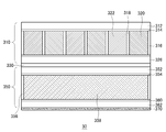
도 3은 본원 발명의 다른 실시예에 따른 반사형 액정 디스플레이 구조를 도시한 단면도이다.
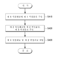
도 4는 본원 발명의 일 실시예에 따른 반사형 액정 디스플레이 장치의 제조 방법을 도시한 도면이다.
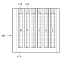
도 5a 내지 도 5d는 본원 발명의 일 실시예에 따른 액정 패널에 대한 액정 주입 방법을 도시한 도면이다.
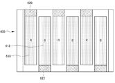
도 6a 및 도 6b는 본원 발명의 다른 실시예에 따른 액정 패널에 대한 액정 주입 방법을 도시한 도면이다.
150: 제 2 액정 패널 170: 광 흡수층
310: 제 1 액정 패널 330: 접착층
350: 제 2 액정 패널 370: 광 흡수층
Claims (17)
- 반사형 액정 디스플레이 장치에 있어서,
제 1 색상의 광을 반사시키는 제 1 액정물질을 포함하는 제 1 액정 패널,
제 2 색상의 광을 반사시키는 제 2 액정물질과 제 3 색상의 광을 반사시키는 제 3 액정물질을 포함하되, 각 액정물질을 서로 구분되게 배치시킨 제 2 액정 패널 및
상기 제 2 액정 패널의 하부에 결합된 광 흡수층을 포함하되,
상기 제 2 액정 패널은 상기 제 1 액정 패널의 하부에 결합된 것이고,
상기 각 액정 물질은 플래나(planar) 상태일 때 광을 반사시키고, 포컬 코닉(focal conic) 상태일 때 광을 통과시키는 것인 반사형 액정 디스플레이 장치. - 반사형 액정 디스플레이 장치에 있어서,
제 1 색상의 광을 반사시키는 제 1 액정물질을 포함하는 제 1 액정 패널
제 2 색상의 광을 반사시키는 제 2 액정물질과 제 3 색상의 광을 반사시키는 제 2 액정물질을 포함하되, 각 액정물질을 서로 구분되게 배치시킨 제 2 액정 패널및
상기 제 1 액정 패널의 하부에 결합된 광 흡수층을 포함하되,
상기 제 1 액정 패널은 상기 제 2 액정 패널의 하부에 결합된 것이고,
상기 각 액정 물질은 플래나(planar) 상태일 때 광을 반사시키고, 포컬 코닉(focal conic) 상태일 때 광을 통과시키는 것인 반사형 액정 디스플레이 장치. - 제 1 항 또는 제 2 항에 있어서,
상기 제 1액정 패널은,
제 1 기판,
상기 제 1 기판의 하부에 결합되고, 서로 대향하도록 배치된 제 1 전극 및 제 2 전극,
상기 제 2 전극의 하부에 결합된 제 2 기판을 포함하되
상기 기판과 전극은 각각 투명하고,
상기 제 1 전극과 제 2 전극 사이에 상기 제 1 액정물질이 충진된 것인
반사형 액정 디스플레이 장치. - 제 1 항 또는 제 2 항에 있어서,
상기 제 2 액정 패널은,
제 1 기판,
상기 제 1 기판의 하부에 결합되고, 서로 대향하도록 배치된 제 1 전극 및 제 2 전극,
상기 제 1 전극과 제 2 전극 사이에 배치되고, 상기 각 액정물질을 분리시키는 하나 이상의 격벽 및
상기 제 2 전극의 하부에 결합된 제 2 기판을 포함하되
상기 기판 및 전극은 각각 투명하고,
상기 격벽에 의하여 분리된 공간들 중 서로 인접한 공간에는 서로 상이한 색상의 광을 반사시키는 액정물질이 충진된 것인 반사형 액정 디스플레이 장치. - 제 3 항 또는 제 4 항에 있어서,
상기 제 1 전극과 제 2 전극에 인가되는 전압에 따라, 상기 액정물질이 플래나 상태 또는 포컬 코닉 상태로 전환되는 것인 반사형 액정 디스플레이 장치. - 제 1 항 또는 제 2 항에 있어서,
상기 제 1 색상 내지 제 3 색상은 R(Red), G(Green) 및 B(Blue) 중 어느 하나이되, 각각의 색상은 서로 상이한 것인 반사형 액정 디스플레이 장치. - 제 1 항 또는 제 2 항에 있어서,
상기 제 1 색상 내지 제 3 색상은 C(Cyan), M(Magenta) 및 Y(Yellow) 중 어느 하나이되, 각각의 색상은 서로 상이한 것인 반사형 액정 디스플레이 장치. - 제 1 항 또는 제 2 항에 있어서,
상기 제 1 액정 물질 내지 제 3 액정 물질은 콜레스테릭(Cholesteric) 액정 물질인 것인 반사형 액정 디스플레이 장치. - 반사형 액정 디스플레이 장치의 제조 방법에 있어서,
(a) 제 1 액정 패널에 제 1 색상의 광을 반사시키는 제 1 액정물질을 주입하는 단계,
(b) 복수의 격벽에 의하여 공간이 구분된 제 2 액정 패널에 제 2 색상의 광을 반사시키는 제 2 액정물질과 제 3 색상의 광을 반사시키는 제 3 액정물질을 주입하는 단계 및
(c) 상기 제 1 액정 패널의 하부에 상기 제 2 액정 패널을 결합시키는 단계
를 포함하는 반사형 액정 디스플레이 장치의 제조 방법. - 제 9 항에 있어서,
상기 제 2 액정 패널의 하부에 광 흡수층을 결합시키는 단계
를 더 포함하는 반사형 액정 디스플레이 장치의 제조 방법. - 반사형 액정 디스플레이 장치의 제조 방법에 있어서,
(a) 제 1 액정 패널에 제 1 색상의 광을 반사시키는 제 1 액정물질을 주입하는 단계,
(b) 복수의 격벽에 의하여 공간이 구분된 제 2 액정 패널에 제 2 색상의 광을 반사시키는 제 2 액정물질과 제 3 색상의 광을 반사시키는 제 3 액정물질을 주입하는 단계 및
(c) 상기 제 1 액정 패널의 상부에 상기 제 2 액정 패널을 결합시키는 단계
를 포함하는 반사형 액정 디스플레이 장치의 제조 방법. - 제 11 항에 있어서,
상기 제 1 액정 패널의 하부에 광 흡수층을 결합시키는 단계
를 더 포함하는 반사형 액정 디스플레이 장치의 제조 방법. - 제 9 항 또는 제 11 항에 있어서,
상기 (b) 단계는,
(b1) 상기 제 2 액정 패널의 격벽에 의하여 구분된 제 1 공간의 주입구에 상기 제 2 액정물질을 주입하는 단계,
(b2) 상기 제 1 공간의 주입구를 실링하는 단계,
(b3) 상기 제 2 액정 패널의 격벽에 의하여 구분된 제 2 공간의 주입구에 상기 제 3 액정물질을 주입하는 단계 및
(b4) 상기 제 2 공간의 주입구를 실링하는 단계를 포함하되,
상기 제 1 공간과 제 2 공간은 상기 격벽을 기준으로 서로 인접한 상태로 나란하게 연장되고,
상기 제 1 공간의 주입구는 상기 제 2 액정 패널의 일측면에 위치하고, 상기 제 2 공간의 주입구 상기 제 2 액정 패널의 일측면과 마주보는 타측면에 위치한 것인 반사형 액정 디스플레이 장치의 제조 방법. - 제 9 항 또는 제 11 항에 있어서,
상기 (b) 단계는,
(b1) 상기 제 2 액정 패널의 격벽에 의하여 구분된 제 1 공간의 주입구에 상기 제 2 액정물질을 주입하는 단계,
(b2) 상기 제 1 공간의 주입구를 실링하는 단계,
(b3) 상기 제 2 액정 패널의 일부를 절삭하여 상기 제 2 공간의 주입구를 개방하는 단계,
(b4) 상기 개방된 제 2 공간의 주입구에 상기 제 3 액정물질을 주입하는 단계 및
(b5) 상기 제 2 공간의 주입구를 실링하는 단계를 포함하되,
상기 제 1 공간과 제 2 공간은 상기 격벽을 기준으로 서로 인접한 상태로 나란하게 연장되고,
상기 (b3) 단계는 상기 제 1 공간의 실링 영역의 일부를 절삭하는 것인 반사형 액정 디스플레이 장치의 제조 방법. - 제 9 항 또는 제 11 항에 있어서,
상기 제 1 색상 내지 제 3 색상은 R(Red), G(Green) 및 B(Blue) 중 어느 하나이되, 각각의 색상은 서로 상이한 것인 반사형 액정 디스플레이 장치의 제조 방법. - 제 9 항 또는 제 11 항에 있어서,
상기 제 1 색상 내지 제 3 색상은 C(Cyan), M(Magenta) 및 Y(Yellow) 중 어느 하나이되, 각각의 색상은 서로 상이한 것인 반사형 액정 디스플레이 장치의 제조 방법. - 제 9 항 또는 제 11 항에 있어서,
상기 제 1 액정 물질 내지 제 3 액정 물질은 콜레스테릭(Cholesteric) 액정 물질인 것인 반사형 액정 디스플레이 장치의 제조 방법.
Priority Applications (3)
| Application Number | Priority Date | Filing Date | Title |
|---|---|---|---|
| KR1020110040562A KR20120122432A (ko) | 2011-04-29 | 2011-04-29 | 반사형 액정 디스플레이 장치 및 그 제조방법 |
| PCT/KR2012/003061 WO2012148133A2 (ko) | 2011-04-29 | 2012-04-20 | 반사형 액정 디스플레이 장치 및 그 제조방법 |
| US13/459,692 US8994897B2 (en) | 2011-04-29 | 2012-04-30 | Reflective liquid crystal display device and method for manufacturing the same |
Applications Claiming Priority (1)
| Application Number | Priority Date | Filing Date | Title |
|---|---|---|---|
| KR1020110040562A KR20120122432A (ko) | 2011-04-29 | 2011-04-29 | 반사형 액정 디스플레이 장치 및 그 제조방법 |
Publications (1)
| Publication Number | Publication Date |
|---|---|
| KR20120122432A true KR20120122432A (ko) | 2012-11-07 |
Family
ID=47067621
Family Applications (1)
| Application Number | Title | Priority Date | Filing Date |
|---|---|---|---|
| KR1020110040562A Ceased KR20120122432A (ko) | 2011-04-29 | 2011-04-29 | 반사형 액정 디스플레이 장치 및 그 제조방법 |
Country Status (3)
| Country | Link |
|---|---|
| US (1) | US8994897B2 (ko) |
| KR (1) | KR20120122432A (ko) |
| WO (1) | WO2012148133A2 (ko) |
Cited By (1)
| Publication number | Priority date | Publication date | Assignee | Title |
|---|---|---|---|---|
| KR101423168B1 (ko) * | 2013-08-05 | 2014-07-28 | 주식회사 네모레이드 | 콘텐츠 표시를 위한 그래픽 유저 인터페이스 제공방법 및 이를 위한 단말 |
Families Citing this family (6)
| Publication number | Priority date | Publication date | Assignee | Title |
|---|---|---|---|---|
| US20170122028A1 (en) * | 2014-07-23 | 2017-05-04 | Panasonic Intellectual Property Management Co., Ltd. | Light control element and building material provided with same |
| KR102367774B1 (ko) * | 2015-06-12 | 2022-02-28 | 삼성전자주식회사 | 디스플레이 장치 |
| US9927672B2 (en) * | 2015-12-16 | 2018-03-27 | Kent Displays Inc. | Multicolored pressure sensitive liquid crystal device |
| CN108022565B (zh) * | 2016-11-02 | 2021-03-30 | 群创光电股份有限公司 | 调整方法以及显示器 |
| CN111708239A (zh) * | 2020-07-06 | 2020-09-25 | 大连龙宁科技有限公司 | 一种双层混色胆甾型液晶电子纸的叠加结构及其贴合方法 |
| CN116203769B (zh) * | 2023-03-03 | 2026-02-24 | 昆山龙腾光电股份有限公司 | 反射式显示屏 |
Family Cites Families (9)
| Publication number | Priority date | Publication date | Assignee | Title |
|---|---|---|---|---|
| US6034752A (en) | 1997-03-22 | 2000-03-07 | Kent Displays Incorporated | Display device reflecting visible and infrared radiation |
| JP3599089B2 (ja) * | 1998-11-11 | 2004-12-08 | 富士ゼロックス株式会社 | 多色表示装置 |
| JP2000227606A (ja) * | 1999-02-05 | 2000-08-15 | Minolta Co Ltd | 液晶表示装置 |
| TWI368069B (en) | 2007-04-14 | 2012-07-11 | Ind Tech Res Inst | Color cholesteric liquid crystal display devices and fabrication methods thereof |
| JP2010039038A (ja) * | 2008-08-01 | 2010-02-18 | Fujitsu Ltd | 表示装置 |
| TWI415045B (zh) * | 2009-02-24 | 2013-11-11 | Ind Tech Res Inst | 反射式顯示器的畫素結構 |
| KR101068771B1 (ko) * | 2009-08-06 | 2011-09-30 | 한국과학기술원 | 투명 디스플레이 장치 |
| JP2011043777A (ja) * | 2009-08-24 | 2011-03-03 | Fuji Xerox Co Ltd | 表示媒体 |
| JP2012088496A (ja) * | 2010-10-19 | 2012-05-10 | Fujitsu Ltd | 反射型カラー液晶表示素子および反射型カラー液晶表示装置 |
-
2011
- 2011-04-29 KR KR1020110040562A patent/KR20120122432A/ko not_active Ceased
-
2012
- 2012-04-20 WO PCT/KR2012/003061 patent/WO2012148133A2/ko not_active Ceased
- 2012-04-30 US US13/459,692 patent/US8994897B2/en not_active Expired - Fee Related
Cited By (1)
| Publication number | Priority date | Publication date | Assignee | Title |
|---|---|---|---|---|
| KR101423168B1 (ko) * | 2013-08-05 | 2014-07-28 | 주식회사 네모레이드 | 콘텐츠 표시를 위한 그래픽 유저 인터페이스 제공방법 및 이를 위한 단말 |
Also Published As
| Publication number | Publication date |
|---|---|
| WO2012148133A2 (ko) | 2012-11-01 |
| WO2012148133A3 (ko) | 2013-01-03 |
| US8994897B2 (en) | 2015-03-31 |
| US20120274886A1 (en) | 2012-11-01 |
Similar Documents
| Publication | Publication Date | Title |
|---|---|---|
| US20120274887A1 (en) | Cholesteric liquid crystal display device and method for manufacturing the same | |
| KR20120122432A (ko) | 반사형 액정 디스플레이 장치 및 그 제조방법 | |
| KR101720587B1 (ko) | 반사형 디스플레이 장치 | |
| US20100053728A1 (en) | Color display devices | |
| US20090244441A1 (en) | Display device | |
| EP2485086A1 (en) | Liquid crystal display panel | |
| US8699120B2 (en) | Display apparatus | |
| KR101490487B1 (ko) | 반사형 액정 디스플레이 및 그 제조 방법 | |
| US20150077687A1 (en) | Liquid crystal display device | |
| KR100453897B1 (ko) | 액정 디스플레이용 로우 패널 및 이 로우 패널을 이용한칼라 액정 디스플레이의 제조 방법 | |
| CN102981323A (zh) | 显示面板、其制造方法以及显示装置 | |
| KR20190070843A (ko) | 편광판 일체형 프라이버시 필름 및 그를 이용한 표시 장치 | |
| US8314904B2 (en) | Pixel structure of reflective display | |
| KR20170076551A (ko) | 액정표시장치 | |
| US20090161052A1 (en) | Display element, electronic paper using the element, and electronic terminal using the element | |
| CN101344668B (zh) | 液晶显示器件及其制造方法 | |
| JP5426071B2 (ja) | 液晶表示装置 | |
| JP2010134128A (ja) | 液晶表示装置および液晶表示装置用枠体 | |
| US20050157231A1 (en) | Transflective mode liquid crystal display | |
| CN106997117A (zh) | 液晶显示装置 | |
| US20120268698A1 (en) | Color filter substrate and display device | |
| WO2015078176A1 (zh) | 显示面板 | |
| US9459486B2 (en) | Liquid crystal display device in which display of off state reflected light is suppressed | |
| US20100315579A1 (en) | Colored liquid crystal display | |
| JP2004029800A (ja) | 液晶表示セルや電気化学的光起電力セルなどの積層セルのバッチ製造方法 |
Legal Events
| Date | Code | Title | Description |
|---|---|---|---|
| A201 | Request for examination | ||
| PA0109 | Patent application |
St.27 status event code: A-0-1-A10-A12-nap-PA0109 |
|
| PA0201 | Request for examination |
St.27 status event code: A-1-2-D10-D11-exm-PA0201 |
|
| P11-X000 | Amendment of application requested |
St.27 status event code: A-2-2-P10-P11-nap-X000 |
|
| P13-X000 | Application amended |
St.27 status event code: A-2-2-P10-P13-nap-X000 |
|
| PN2301 | Change of applicant |
St.27 status event code: A-3-3-R10-R13-asn-PN2301 St.27 status event code: A-3-3-R10-R11-asn-PN2301 |
|
| D13-X000 | Search requested |
St.27 status event code: A-1-2-D10-D13-srh-X000 |
|
| D14-X000 | Search report completed |
St.27 status event code: A-1-2-D10-D14-srh-X000 |
|
| E902 | Notification of reason for refusal | ||
| PE0902 | Notice of grounds for rejection |
St.27 status event code: A-1-2-D10-D21-exm-PE0902 |
|
| AMND | Amendment | ||
| E13-X000 | Pre-grant limitation requested |
St.27 status event code: A-2-3-E10-E13-lim-X000 |
|
| P11-X000 | Amendment of application requested |
St.27 status event code: A-2-2-P10-P11-nap-X000 |
|
| P13-X000 | Application amended |
St.27 status event code: A-2-2-P10-P13-nap-X000 |
|
| PG1501 | Laying open of application |
St.27 status event code: A-1-1-Q10-Q12-nap-PG1501 |
|
| E601 | Decision to refuse application | ||
| PE0601 | Decision on rejection of patent |
St.27 status event code: N-2-6-B10-B15-exm-PE0601 |
|
| AMND | Amendment | ||
| P11-X000 | Amendment of application requested |
St.27 status event code: A-2-2-P10-P11-nap-X000 |
|
| P13-X000 | Application amended |
St.27 status event code: A-2-2-P10-P13-nap-X000 |
|
| PX0901 | Re-examination |
St.27 status event code: A-2-3-E10-E12-rex-PX0901 |
|
| PX0601 | Decision of rejection after re-examination |
St.27 status event code: N-2-6-B10-B17-rex-PX0601 |
|
| J201 | Request for trial against refusal decision | ||
| PJ0201 | Trial against decision of rejection |
St.27 status event code: A-3-3-V10-V11-apl-PJ0201 |
|
| J301 | Trial decision |
Free format text: TRIAL DECISION FOR APPEAL AGAINST DECISION TO DECLINE REFUSAL REQUESTED 20130516 Effective date: 20140919 |
|
| PJ1301 | Trial decision |
St.27 status event code: A-3-3-V10-V15-crt-PJ1301 Decision date: 20140919 Appeal event data comment text: Appeal Kind Category : Appeal against decision to decline refusal, Appeal Ground Text : 2011 0040562 Appeal request date: 20130516 Appellate body name: Patent Examination Board Decision authority category: Office appeal board Decision identifier: 2013101003674 |
|
| R18-X000 | Changes to party contact information recorded |
St.27 status event code: A-3-3-R10-R18-oth-X000 |
|
| R18-X000 | Changes to party contact information recorded |
St.27 status event code: A-3-3-R10-R18-oth-X000 |
|
| R18-X000 | Changes to party contact information recorded |
St.27 status event code: A-3-3-R10-R18-oth-X000 |
|
| PN2301 | Change of applicant |
St.27 status event code: A-3-3-R10-R13-asn-PN2301 St.27 status event code: A-3-3-R10-R11-asn-PN2301 |
|
| R18-X000 | Changes to party contact information recorded |
St.27 status event code: A-3-3-R10-R18-oth-X000 |
|
| R18 | Changes to party contact information recorded |
Free format text: ST27 STATUS EVENT CODE: A-3-3-R10-R18-OTH-X000 (AS PROVIDED BY THE NATIONAL OFFICE) |
|
| R18-X000 | Changes to party contact information recorded |
St.27 status event code: A-3-3-R10-R18-oth-X000 |