KR20120133558A - 백라이트 유닛 - Google Patents
백라이트 유닛 Download PDFInfo
- Publication number
- KR20120133558A KR20120133558A KR1020110052266A KR20110052266A KR20120133558A KR 20120133558 A KR20120133558 A KR 20120133558A KR 1020110052266 A KR1020110052266 A KR 1020110052266A KR 20110052266 A KR20110052266 A KR 20110052266A KR 20120133558 A KR20120133558 A KR 20120133558A
- Authority
- KR
- South Korea
- Prior art keywords
- guide plate
- light
- light emitting
- emitting device
- light guide
- Prior art date
- Legal status (The legal status is an assumption and is not a legal conclusion. Google has not performed a legal analysis and makes no representation as to the accuracy of the status listed.)
- Ceased
Links
- 230000003287 optical effect Effects 0.000 claims abstract description 37
- 238000000034 method Methods 0.000 claims description 13
- 239000010408 film Substances 0.000 description 23
- 239000004973 liquid crystal related substance Substances 0.000 description 21
- 239000000758 substrate Substances 0.000 description 8
- 238000009792 diffusion process Methods 0.000 description 6
- 239000010409 thin film Substances 0.000 description 6
- 239000011347 resin Substances 0.000 description 4
- 229920005989 resin Polymers 0.000 description 4
- 230000001681 protective effect Effects 0.000 description 3
- 239000004925 Acrylic resin Substances 0.000 description 2
- 229920000178 Acrylic resin Polymers 0.000 description 2
- JMASRVWKEDWRBT-UHFFFAOYSA-N Gallium nitride Chemical compound [Ga]#N JMASRVWKEDWRBT-UHFFFAOYSA-N 0.000 description 2
- 150000001875 compounds Chemical class 0.000 description 2
- 239000008393 encapsulating agent Substances 0.000 description 2
- 239000011521 glass Substances 0.000 description 2
- 230000006872 improvement Effects 0.000 description 2
- 229910052751 metal Inorganic materials 0.000 description 2
- 239000002184 metal Substances 0.000 description 2
- 238000010295 mobile communication Methods 0.000 description 2
- 239000002245 particle Substances 0.000 description 2
- 229920003229 poly(methyl methacrylate) Polymers 0.000 description 2
- 239000004926 polymethyl methacrylate Substances 0.000 description 2
- 239000004065 semiconductor Substances 0.000 description 2
- 238000002834 transmittance Methods 0.000 description 2
- JBRZTFJDHDCESZ-UHFFFAOYSA-N AsGa Chemical compound [As]#[Ga] JBRZTFJDHDCESZ-UHFFFAOYSA-N 0.000 description 1
- RYGMFSIKBFXOCR-UHFFFAOYSA-N Copper Chemical compound [Cu] RYGMFSIKBFXOCR-UHFFFAOYSA-N 0.000 description 1
- 239000004593 Epoxy Substances 0.000 description 1
- 229910002601 GaN Inorganic materials 0.000 description 1
- OAICVXFJPJFONN-UHFFFAOYSA-N Phosphorus Chemical compound [P] OAICVXFJPJFONN-UHFFFAOYSA-N 0.000 description 1
- 238000000149 argon plasma sintering Methods 0.000 description 1
- 239000011324 bead Substances 0.000 description 1
- 230000005540 biological transmission Effects 0.000 description 1
- 230000015572 biosynthetic process Effects 0.000 description 1
- 239000011248 coating agent Substances 0.000 description 1
- 238000000576 coating method Methods 0.000 description 1
- 239000003086 colorant Substances 0.000 description 1
- 229910052802 copper Inorganic materials 0.000 description 1
- 239000010949 copper Substances 0.000 description 1
- 230000007547 defect Effects 0.000 description 1
- 238000010586 diagram Methods 0.000 description 1
- 230000017525 heat dissipation Effects 0.000 description 1
- 229910052738 indium Inorganic materials 0.000 description 1
- APFVFJFRJDLVQX-UHFFFAOYSA-N indium atom Chemical compound [In] APFVFJFRJDLVQX-UHFFFAOYSA-N 0.000 description 1
- 238000009413 insulation Methods 0.000 description 1
- 239000000463 material Substances 0.000 description 1
- 238000012986 modification Methods 0.000 description 1
- 230000004048 modification Effects 0.000 description 1
- 239000012788 optical film Substances 0.000 description 1
- 239000004033 plastic Substances 0.000 description 1
- 229920003023 plastic Polymers 0.000 description 1
- 229920000515 polycarbonate Polymers 0.000 description 1
- 239000004417 polycarbonate Substances 0.000 description 1
- 229920000647 polyepoxide Polymers 0.000 description 1
- 229920000728 polyester Polymers 0.000 description 1
- 230000008569 process Effects 0.000 description 1
- 230000004044 response Effects 0.000 description 1
- 229920002050 silicone resin Polymers 0.000 description 1
- 239000013585 weight reducing agent Substances 0.000 description 1
Images




Classifications
-
- G—PHYSICS
- G02—OPTICS
- G02F—OPTICAL DEVICES OR ARRANGEMENTS FOR THE CONTROL OF LIGHT BY MODIFICATION OF THE OPTICAL PROPERTIES OF THE MEDIA OF THE ELEMENTS INVOLVED THEREIN; NON-LINEAR OPTICS; FREQUENCY-CHANGING OF LIGHT; OPTICAL LOGIC ELEMENTS; OPTICAL ANALOGUE/DIGITAL CONVERTERS
- G02F1/00—Devices or arrangements for the control of the intensity, colour, phase, polarisation or direction of light arriving from an independent light source, e.g. switching, gating or modulating; Non-linear optics
- G02F1/01—Devices or arrangements for the control of the intensity, colour, phase, polarisation or direction of light arriving from an independent light source, e.g. switching, gating or modulating; Non-linear optics for the control of the intensity, phase, polarisation or colour
- G02F1/13—Devices or arrangements for the control of the intensity, colour, phase, polarisation or direction of light arriving from an independent light source, e.g. switching, gating or modulating; Non-linear optics for the control of the intensity, phase, polarisation or colour based on liquid crystals, e.g. single liquid crystal display cells
- G02F1/133—Constructional arrangements; Operation of liquid crystal cells; Circuit arrangements
- G02F1/1333—Constructional arrangements; Manufacturing methods
- G02F1/1335—Structural association of cells with optical devices, e.g. polarisers or reflectors
- G02F1/1336—Illuminating devices
-
- G—PHYSICS
- G02—OPTICS
- G02B—OPTICAL ELEMENTS, SYSTEMS OR APPARATUS
- G02B6/00—Light guides; Structural details of arrangements comprising light guides and other optical elements, e.g. couplings
- G02B6/0001—Light guides; Structural details of arrangements comprising light guides and other optical elements, e.g. couplings specially adapted for lighting devices or systems
- G02B6/0011—Light guides; Structural details of arrangements comprising light guides and other optical elements, e.g. couplings specially adapted for lighting devices or systems the light guides being planar or of plate-like form
- G02B6/0013—Means for improving the coupling-in of light from the light source into the light guide
- G02B6/0015—Means for improving the coupling-in of light from the light source into the light guide provided on the surface of the light guide or in the bulk of it
- G02B6/002—Means for improving the coupling-in of light from the light source into the light guide provided on the surface of the light guide or in the bulk of it by shaping at least a portion of the light guide, e.g. with collimating, focussing or diverging surfaces
-
- G—PHYSICS
- G02—OPTICS
- G02B—OPTICAL ELEMENTS, SYSTEMS OR APPARATUS
- G02B6/00—Light guides; Structural details of arrangements comprising light guides and other optical elements, e.g. couplings
- G02B6/0001—Light guides; Structural details of arrangements comprising light guides and other optical elements, e.g. couplings specially adapted for lighting devices or systems
- G02B6/0011—Light guides; Structural details of arrangements comprising light guides and other optical elements, e.g. couplings specially adapted for lighting devices or systems the light guides being planar or of plate-like form
- G02B6/0033—Means for improving the coupling-out of light from the light guide
- G02B6/0035—Means for improving the coupling-out of light from the light guide provided on the surface of the light guide or in the bulk of it
- G02B6/0045—Means for improving the coupling-out of light from the light guide provided on the surface of the light guide or in the bulk of it by shaping at least a portion of the light guide
- G02B6/0046—Tapered light guide, e.g. wedge-shaped light guide
-
- G—PHYSICS
- G02—OPTICS
- G02F—OPTICAL DEVICES OR ARRANGEMENTS FOR THE CONTROL OF LIGHT BY MODIFICATION OF THE OPTICAL PROPERTIES OF THE MEDIA OF THE ELEMENTS INVOLVED THEREIN; NON-LINEAR OPTICS; FREQUENCY-CHANGING OF LIGHT; OPTICAL LOGIC ELEMENTS; OPTICAL ANALOGUE/DIGITAL CONVERTERS
- G02F1/00—Devices or arrangements for the control of the intensity, colour, phase, polarisation or direction of light arriving from an independent light source, e.g. switching, gating or modulating; Non-linear optics
- G02F1/01—Devices or arrangements for the control of the intensity, colour, phase, polarisation or direction of light arriving from an independent light source, e.g. switching, gating or modulating; Non-linear optics for the control of the intensity, phase, polarisation or colour
- G02F1/13—Devices or arrangements for the control of the intensity, colour, phase, polarisation or direction of light arriving from an independent light source, e.g. switching, gating or modulating; Non-linear optics for the control of the intensity, phase, polarisation or colour based on liquid crystals, e.g. single liquid crystal display cells
- G02F1/133—Constructional arrangements; Operation of liquid crystal cells; Circuit arrangements
- G02F1/1333—Constructional arrangements; Manufacturing methods
- G02F1/1335—Structural association of cells with optical devices, e.g. polarisers or reflectors
- G02F1/1336—Illuminating devices
- G02F1/133615—Edge-illuminating devices, i.e. illuminating from the side
-
- G—PHYSICS
- G02—OPTICS
- G02B—OPTICAL ELEMENTS, SYSTEMS OR APPARATUS
- G02B6/00—Light guides; Structural details of arrangements comprising light guides and other optical elements, e.g. couplings
- G02B6/0001—Light guides; Structural details of arrangements comprising light guides and other optical elements, e.g. couplings specially adapted for lighting devices or systems
- G02B6/0011—Light guides; Structural details of arrangements comprising light guides and other optical elements, e.g. couplings specially adapted for lighting devices or systems the light guides being planar or of plate-like form
- G02B6/0033—Means for improving the coupling-out of light from the light guide
- G02B6/005—Means for improving the coupling-out of light from the light guide provided by one optical element, or plurality thereof, placed on the light output side of the light guide
-
- G—PHYSICS
- G02—OPTICS
- G02B—OPTICAL ELEMENTS, SYSTEMS OR APPARATUS
- G02B6/00—Light guides; Structural details of arrangements comprising light guides and other optical elements, e.g. couplings
- G02B6/0001—Light guides; Structural details of arrangements comprising light guides and other optical elements, e.g. couplings specially adapted for lighting devices or systems
- G02B6/0011—Light guides; Structural details of arrangements comprising light guides and other optical elements, e.g. couplings specially adapted for lighting devices or systems the light guides being planar or of plate-like form
- G02B6/0066—Light guides; Structural details of arrangements comprising light guides and other optical elements, e.g. couplings specially adapted for lighting devices or systems the light guides being planar or of plate-like form characterised by the light source being coupled to the light guide
- G02B6/0068—Arrangements of plural sources, e.g. multi-colour light sources
Landscapes
- Physics & Mathematics (AREA)
- General Physics & Mathematics (AREA)
- Optics & Photonics (AREA)
- Nonlinear Science (AREA)
- Mathematical Physics (AREA)
- Chemical & Material Sciences (AREA)
- Crystallography & Structural Chemistry (AREA)
- Planar Illumination Modules (AREA)
Abstract
Description
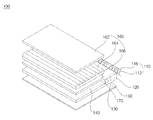
도 1b 는 실시예에 따른 백라이트 유닛을 나타낸 일부 분해 사시도,
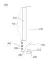
도 2a 는 실시예에 따른 백라이트 유닛의 일부를 나타낸 단면도,
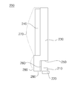
도 2b 는 실시예에 따른 백라이트 유닛의 일부를 나타낸 단면도,
도 2c 는 실시예에 따른 백라이트 유닛의 일부를 나타낸 단면도,
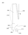
도 2d 는 실시예에 따른 백라이트 유닛의 일부를 나타낸 단면도,
도 3 은 실시예에 따른 백라이트 유닛을 포함한 액정표시장치를 나타낸 분해 사시도, 그리고,
도 4 는 실시예에 따른 백라이트 유닛을 포함한 전자 기기를 나타낸 개념도이다.
120 : 도광판 130 : 제1 영역
140 : 제2 영역 150 : 반사시트
160 : 광학시트 170 : 단차면
Claims (12)
- 발광소자 패키지;
상기 발광소자 패키지와 인접하는 측면에 함몰된 홈을 포함하는 제1 영역, 및 상기 제1 영역과 상면에 단차를 형성하는 제2 영역을 포함하는 도광판; 및
상기 제2 영역의 상면에 구비되는 광학시트;를 포함하는 백라이트 유닛. - 제1항에 있어서,
상기 홈은 상기 도광판의 하면과 측면이 함께 함몰되어 형성되는 백라이트 유닛. - 제1항에 있어서,
상기 도광판의 상면은 상기 제1 영역이 돌출된 백라이트 유닛. - 제1항에 있어서,
상기 제1 영역과 상기 제2 영역의 단차는 0.5 내지 1.0mm인 백라이트 유닛. - 제1항에 있어서,
상기 홈의 일측면은 상기 도광판의 상면과 평행하게 형성되고, 그 위에 반사판이 구비되는 백라이트 유닛. - 제1항에 있어서,
상기 홈의 윤곽은 곡률을 갖는 백라이트 유닛. - 제1항에 있어서,
상기 홈에 상기 발광소자 패키지가 배치되는 백라이트 유닛. - 제2항에 있어서,
상기 홈의 상기 도광판의 하면으로부터 함몰된 깊이는 상기 도광판의 측면으로부터 함몰된 깊이의 1 내지 5배인 백라이트 유닛. - 제1항에 있어서,
상기 발광소자 패키지와 인접하는 상기 도광판의 측면의 수직방향으로의 상기 제2 영역의 길이는 상기 제1 영역의 길이의 20 내지 80배인 백라이트 유닛. - 제1항에 있어서,
상기 제1 영역의 상면에 패턴이 구비된 백라이트 유닛. - 제1항에 있어서,
상기 제2 영역의 하면에 배치되는 반사시트를 더 포함하는 백라이트 유닛. - 제1항에 대하여,
상기 제2 영역의 하면은 경사각을 갖는 백라이트 유닛.
Priority Applications (4)
| Application Number | Priority Date | Filing Date | Title |
|---|---|---|---|
| KR1020110052266A KR20120133558A (ko) | 2011-05-31 | 2011-05-31 | 백라이트 유닛 |
| US13/473,701 US8882322B2 (en) | 2011-05-31 | 2012-05-17 | Backlight unit |
| EP12168733.9A EP2530375B1 (en) | 2011-05-31 | 2012-05-21 | Light guide design for edge-illumination in a backlight unit |
| CN201210176073.7A CN102809090B (zh) | 2011-05-31 | 2012-05-31 | 背光单元 |
Applications Claiming Priority (1)
| Application Number | Priority Date | Filing Date | Title |
|---|---|---|---|
| KR1020110052266A KR20120133558A (ko) | 2011-05-31 | 2011-05-31 | 백라이트 유닛 |
Publications (1)
| Publication Number | Publication Date |
|---|---|
| KR20120133558A true KR20120133558A (ko) | 2012-12-11 |
Family
ID=46147326
Family Applications (1)
| Application Number | Title | Priority Date | Filing Date |
|---|---|---|---|
| KR1020110052266A Ceased KR20120133558A (ko) | 2011-05-31 | 2011-05-31 | 백라이트 유닛 |
Country Status (4)
| Country | Link |
|---|---|
| US (1) | US8882322B2 (ko) |
| EP (1) | EP2530375B1 (ko) |
| KR (1) | KR20120133558A (ko) |
| CN (1) | CN102809090B (ko) |
Families Citing this family (7)
| Publication number | Priority date | Publication date | Assignee | Title |
|---|---|---|---|---|
| KR102164531B1 (ko) * | 2014-02-05 | 2020-10-12 | 엘지이노텍 주식회사 | 조명 장치 |
| US9423665B2 (en) | 2014-03-24 | 2016-08-23 | Industrial Technology Research Institute | Ambient light adjustment apparatus, method and system |
| KR102181945B1 (ko) * | 2014-05-14 | 2020-11-23 | 엘지이노텍 주식회사 | 광원 모듈 및 이를 구비하는 조명 장치 |
| KR102244427B1 (ko) | 2014-06-02 | 2021-04-27 | 엘지이노텍 주식회사 | 조명 장치 |
| CN105448195A (zh) * | 2015-12-16 | 2016-03-30 | 小米科技有限责任公司 | 一种显示装置及电子设备 |
| CN110568942B (zh) * | 2019-05-02 | 2023-05-26 | 义隆电子股份有限公司 | 发光触摸板 |
| CN113238316A (zh) * | 2021-05-20 | 2021-08-10 | 北京京东方光电科技有限公司 | 导光板、背光模组及其制备方法、显示面板 |
Family Cites Families (9)
| Publication number | Priority date | Publication date | Assignee | Title |
|---|---|---|---|---|
| JPH03107821A (ja) | 1989-09-21 | 1991-05-08 | Nippon Steel Corp | 液晶ディスプレイ装置 |
| CN1145832C (zh) * | 1995-03-31 | 2004-04-14 | 精工爱普生株式会社 | 液晶显示装置 |
| CN1504767A (zh) * | 2002-11-29 | 2004-06-16 | 鸿富锦精密工业(深圳)有限公司 | 导光板及采用该导光板的光源系统 |
| CN2731497Y (zh) * | 2004-08-05 | 2005-10-05 | 西安海晶光电科技有限公司 | 超薄液晶模块背光源 |
| CN2763842Y (zh) * | 2004-12-17 | 2006-03-08 | 群康科技(深圳)有限公司 | 背光模组 |
| US7780330B2 (en) | 2007-05-16 | 2010-08-24 | Rohm And Haas Electronics Materials Llc | Elongated illuminators configuration for LCD displays |
| JP2009199866A (ja) * | 2008-02-21 | 2009-09-03 | Hitachi Displays Ltd | 液晶表示装置 |
| US8228464B2 (en) | 2009-01-19 | 2012-07-24 | Hitachi Displays, Ltd. | Liquid crystal display device |
| CN201401733Y (zh) * | 2009-04-23 | 2010-02-10 | 华映光电股份有限公司 | 导光板及其背光模组 |
-
2011
- 2011-05-31 KR KR1020110052266A patent/KR20120133558A/ko not_active Ceased
-
2012
- 2012-05-17 US US13/473,701 patent/US8882322B2/en active Active
- 2012-05-21 EP EP12168733.9A patent/EP2530375B1/en not_active Not-in-force
- 2012-05-31 CN CN201210176073.7A patent/CN102809090B/zh active Active
Also Published As
| Publication number | Publication date |
|---|---|
| EP2530375A1 (en) | 2012-12-05 |
| US20120307522A1 (en) | 2012-12-06 |
| US8882322B2 (en) | 2014-11-11 |
| CN102809090A (zh) | 2012-12-05 |
| CN102809090B (zh) | 2017-11-24 |
| EP2530375B1 (en) | 2018-04-11 |
Similar Documents
| Publication | Publication Date | Title |
|---|---|---|
| KR101824884B1 (ko) | 백라이트 유닛 | |
| JP5329548B2 (ja) | 薄型側面発光ledを用いた薄型バックライト | |
| US7652301B2 (en) | Optical element coupled to low profile side emitting LED | |
| CN105607340B (zh) | 显示装置 | |
| CN102165344A (zh) | 具有光学耦合到后表面的led的薄边缘背光 | |
| CN102378930A (zh) | 包括半导体发光装置的背光 | |
| CN215867453U (zh) | 一种显示装置 | |
| US8882322B2 (en) | Backlight unit | |
| CN104359051A (zh) | 一种背光模组及显示装置 | |
| CN101846251A (zh) | 半导体发光装置及其制作方法、液晶显示装置用背光灯 | |
| JP2011238448A (ja) | バックライトおよびその製造方法、および液晶表示装置 | |
| KR102512909B1 (ko) | 백라이트유니트 및 표시장치 | |
| CN110783433B (zh) | 发光装置与液晶显示器 | |
| KR101991124B1 (ko) | 엘이디 어레이 유닛, 이를 갖는 직하형 백라이트 유닛 및 이를 갖는 표시장치 | |
| CN216979527U (zh) | 背光模组及显示装置 | |
| KR20150025437A (ko) | 광원 모듈 및 이를 구비한 백라이트 유닛 | |
| WO2011074410A1 (ja) | 照明装置、表示装置、及びテレビ受信装置 | |
| CN204100057U (zh) | 一种背光模组及显示装置 | |
| KR101824881B1 (ko) | 백라이트 유닛 | |
| KR20130013971A (ko) | 백라이트 유닛 | |
| KR20130000815A (ko) | 백라이트 유닛 | |
| WO2023173869A1 (zh) | 一种显示设备 | |
| KR101221920B1 (ko) | 발광 소자 패키지 및 이를 이용한 백라이트 유닛 | |
| KR102012353B1 (ko) | 발광다이오드 모듈과, 이를 포함하는 백라이트 유닛 및 디스플레이 장치 | |
| KR20120037642A (ko) | 백라이트 유닛 및 이를 포함하는 표시 장치 |
Legal Events
| Date | Code | Title | Description |
|---|---|---|---|
| PA0109 | Patent application |
Patent event code: PA01091R01D Comment text: Patent Application Patent event date: 20110531 |
|
| PG1501 | Laying open of application | ||
| A201 | Request for examination | ||
| PA0201 | Request for examination |
Patent event code: PA02012R01D Patent event date: 20160411 Comment text: Request for Examination of Application Patent event code: PA02011R01I Patent event date: 20110531 Comment text: Patent Application |
|
| E902 | Notification of reason for refusal | ||
| PE0902 | Notice of grounds for rejection |
Comment text: Notification of reason for refusal Patent event date: 20170314 Patent event code: PE09021S01D |
|
| E601 | Decision to refuse application | ||
| PE0601 | Decision on rejection of patent |
Patent event date: 20170523 Comment text: Decision to Refuse Application Patent event code: PE06012S01D Patent event date: 20170314 Comment text: Notification of reason for refusal Patent event code: PE06011S01I |