KR20130103358A - 종형 트렌치 igbt 및 그 제조방법 - Google Patents
종형 트렌치 igbt 및 그 제조방법 Download PDFInfo
- Publication number
- KR20130103358A KR20130103358A KR1020130019631A KR20130019631A KR20130103358A KR 20130103358 A KR20130103358 A KR 20130103358A KR 1020130019631 A KR1020130019631 A KR 1020130019631A KR 20130019631 A KR20130019631 A KR 20130019631A KR 20130103358 A KR20130103358 A KR 20130103358A
- Authority
- KR
- South Korea
- Prior art keywords
- layer
- body layer
- type
- trench
- polysilicon film
- Prior art date
- Legal status (The legal status is an assumption and is not a legal conclusion. Google has not performed a legal analysis and makes no representation as to the accuracy of the status listed.)
- Granted
Links
Images




Classifications
-
- H—ELECTRICITY
- H10—SEMICONDUCTOR DEVICES; ELECTRIC SOLID-STATE DEVICES NOT OTHERWISE PROVIDED FOR
- H10D—INORGANIC ELECTRIC SEMICONDUCTOR DEVICES
- H10D12/00—Bipolar devices controlled by the field effect, e.g. insulated-gate bipolar transistors [IGBT]
- H10D12/01—Manufacture or treatment
- H10D12/031—Manufacture or treatment of IGBTs
- H10D12/032—Manufacture or treatment of IGBTs of vertical IGBTs
- H10D12/038—Manufacture or treatment of IGBTs of vertical IGBTs having a recessed gate, e.g. trench-gate IGBTs
-
- H—ELECTRICITY
- H10—SEMICONDUCTOR DEVICES; ELECTRIC SOLID-STATE DEVICES NOT OTHERWISE PROVIDED FOR
- H10P—GENERIC PROCESSES OR APPARATUS FOR THE MANUFACTURE OR TREATMENT OF DEVICES COVERED BY CLASS H10
- H10P10/00—Bonding of wafers, substrates or parts of devices
-
- H—ELECTRICITY
- H10—SEMICONDUCTOR DEVICES; ELECTRIC SOLID-STATE DEVICES NOT OTHERWISE PROVIDED FOR
- H10D—INORGANIC ELECTRIC SEMICONDUCTOR DEVICES
- H10D12/00—Bipolar devices controlled by the field effect, e.g. insulated-gate bipolar transistors [IGBT]
-
- H—ELECTRICITY
- H10—SEMICONDUCTOR DEVICES; ELECTRIC SOLID-STATE DEVICES NOT OTHERWISE PROVIDED FOR
- H10D—INORGANIC ELECTRIC SEMICONDUCTOR DEVICES
- H10D12/00—Bipolar devices controlled by the field effect, e.g. insulated-gate bipolar transistors [IGBT]
- H10D12/411—Insulated-gate bipolar transistors [IGBT]
- H10D12/441—Vertical IGBTs
- H10D12/461—Vertical IGBTs having non-planar surfaces, e.g. having trenches, recesses or pillars in the surfaces of the emitter, base or collector regions
- H10D12/481—Vertical IGBTs having non-planar surfaces, e.g. having trenches, recesses or pillars in the surfaces of the emitter, base or collector regions having gate structures on slanted surfaces, on vertical surfaces, or in grooves, e.g. trench gate IGBTs
-
- H—ELECTRICITY
- H10—SEMICONDUCTOR DEVICES; ELECTRIC SOLID-STATE DEVICES NOT OTHERWISE PROVIDED FOR
- H10D—INORGANIC ELECTRIC SEMICONDUCTOR DEVICES
- H10D62/00—Semiconductor bodies, or regions thereof, of devices having potential barriers
- H10D62/10—Shapes, relative sizes or dispositions of the regions of the semiconductor bodies; Shapes of the semiconductor bodies
- H10D62/124—Shapes, relative sizes or dispositions of the regions of semiconductor bodies or of junctions between the regions
- H10D62/126—Top-view geometrical layouts of the regions or the junctions
- H10D62/127—Top-view geometrical layouts of the regions or the junctions of cellular field-effect devices, e.g. multicellular DMOS transistors or IGBTs
-
- H—ELECTRICITY
- H10—SEMICONDUCTOR DEVICES; ELECTRIC SOLID-STATE DEVICES NOT OTHERWISE PROVIDED FOR
- H10D—INORGANIC ELECTRIC SEMICONDUCTOR DEVICES
- H10D62/00—Semiconductor bodies, or regions thereof, of devices having potential barriers
- H10D62/10—Shapes, relative sizes or dispositions of the regions of the semiconductor bodies; Shapes of the semiconductor bodies
- H10D62/13—Semiconductor regions connected to electrodes carrying current to be rectified, amplified or switched, e.g. source or drain regions
- H10D62/141—Anode or cathode regions of thyristors; Collector or emitter regions of gated bipolar-mode devices, e.g. of IGBTs
- H10D62/148—Cathode regions of thyristors
Landscapes
- Electrodes Of Semiconductors (AREA)
Abstract
Description
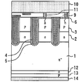
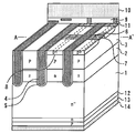
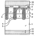
도 2는 도 1의 A-A'에 따른 단면도다.
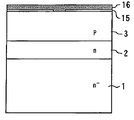
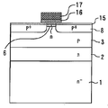
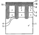
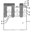
도 3은 본 발명의 실시형태 1에 관한 종형 트렌치 IGBT의 제조방법을 나타낸 단면도다.
도 4는 본 발명의 실시형태 1에 관한 종형 트렌치 IGBT의 제조방법을 나타낸 단면도다.
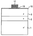
도 5는 본 발명의 실시형태 1에 관한 종형 트렌치 IGBT의 제조방법을 나타낸 단면도다.
도 6은 본 발명의 실시형태 1에 관한 종형 트렌치 IGBT의 제조방법을 나타낸 단면도다.
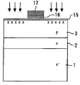
도 7은 본 발명의 실시형태 1에 관한 종형 트렌치 IGBT의 제조방법을 나타낸 단면도다.
도 8은 본 발명의 실시형태 1에 관한 종형 트렌치 IGBT의 제조방법을 나타낸 단면도다.
도 9는 본 발명의 실시형태 1에 관한 종형 트렌치 IGBT의 제조방법을 나타낸 단면도다.
도 10은 비교예에 관한 트렌치 IGBT의 제조방법을 나타낸 단면도다.
도 11은 비교예에 관한 트렌치 IGBT의 동작을 설명하기 위한 단면도다.
도 12는 본 발명의 실시형태 1에 관한 종형 트렌치 IGBT의 변형예를 나타낸 사시도다.
도 13은 도 12의 A-A'에 따른 단면도다.
도 14는 본 발명의 실시형태 2에 관한 종형 트렌치 IGBT를 나타낸 사시도다.
도 15는 도 14의 A-A'에 따른 단면도다.
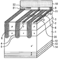
3 p형 보디층(보디층)
4 트렌치 게이트
5 게이트 절연막
6 n형 에미터층(에미터층, 진성 에미터층)
7 n+형 에미터층(에미터층, 외부 에미터층)
8 p+형 확산층(확산층)
9 층간 절연막
10 에미터 전극
11 콘택 플러그
13 p형 콜렉터층(콜렉터층)
16, 20 폴리실리콘 막
17 레지스트
18 자연 산화막
21 용량의 전극
22 폴리실리콘 저항
Claims (9)
- 제1도전형의 반도체 기판 위에 제2도전형의 보디층을 형성하는 공정과,
상기 보디층을 관통하는 트렌치를 형성하고, 상기 트렌치 내부에 게이트 절연막을 개재하여 트렌치 게이트를 형성하는 공정과,
상기 보디층 위에 제1도전형의 불순물을 포함하는 폴리실리콘 막을 형성하는 공정과,
상기 폴리실리콘 막으로부터 상기 보디층에 상기 제1도전형의 불순물을 확산시켜 상기 보디층 위에 제1도전형의 에미터층을 형성하는 공정과,
상기 반도체 기판의 밑면에 제2도전형의 콜렉터층을 형성하는 공정을 구비한 종형 트렌치 IGBT의 제조방법.
- 제 1항에 있어서,
나중에 상기 에미터층을 형성할 영역에 있어서 상기 폴리실리콘 막 위에 레지스트를 형성하는 공정과,
상기 레지스트를 마스크로 하여 상기 폴리실리콘 막을 에칭하는 공정과,
상기 폴리실리콘 막을 에칭한 후에, 상기 레지스트를 마스크로 하여 상기 보디층에 제2도전형의 불순물을 주입하는 공정과,
열처리를 행해서 상기 보디층의 상기 제2도전형의 불순물을 주입한 영역에 제2도전형의 확산층을 형성하는 공정을 더 구비한 종형 트렌치 IGBT의 제조방법.
- 제 1항 또는 제 2항에 있어서,
상기 폴리실리콘 막의 그레인 사이즈는 상기 에미터층의 폭보다 작은 종형 트렌치 IGBT의 제조방법.
- 제 1항 또는 제 2항에 있어서,
상기 보디층과 상기 폴리실리콘 막 사이에 자연 산화막이 형성되어 있는 종형 트렌치 IGBT의 제조방법.
- 제 1항 또는 제 2항에 있어서,
상기 폴리실리콘 막을, 상기 트렌치 게이트를 구성하는 폴리실리콘과 동시에 형성하는 종형 트렌치 IGBT의 제조방법.
- 제 1항 또는 제 2항에 있어서,
상기 폴리실리콘 막을, 용량의 전극을 구성하는 폴리실리콘과 동시에 형성하는 종형 트렌치 IGBT의 제조방법.
- 제 1항 또는 제 2항에 있어서,
상기 폴리실리콘 막을 폴리실리콘 저항과 동시에 형성하는 종형 트렌치 IGBT의 제조방법.
- 제 1항 또는 제 2항에 있어서,
상기 에미터층은,
상기 트렌치 게이트의 근방에 형성된 진성 에미터층과,
상기 진성 에미터층을 외부로 인출하는 외부 에미터층을 갖는 종형 트렌치 IGBT의 제조방법.
- 제1도전형의 반도체 기판과,
상기 반도체 기판 위에 설치된 제2도전형의 보디층과,
상기 보디층을 관통하는 트렌치 내부에 게이트 절연막을 개재하여 설치된 트렌치 게이트와,
상기 보디층 위에 설치된 제1도전형의 에미터층과,
상기 반도체 기판의 밑면에 설치된 제2도전형의 콜렉터층과,
상기 트렌치 게이트를 덮는 층간 절연막과,
상기 층간 절연막 위에 설치된 에미터 전극과
상기 층간 절연막을 관통해서 상기 보디층 및 상기 에미터층과 상기 에미터 전극을 접속하는 콘택 플러그와,
상기 보디층 및 상기 에미터층의 적어도 한쪽과 상기 콘택 플러그 사이에 설치된 폴리실리콘 막을 구비한 종형 트렌치 IGBT.
Applications Claiming Priority (2)
| Application Number | Priority Date | Filing Date | Title |
|---|---|---|---|
| JPJP-P-2012-052580 | 2012-03-09 | ||
| JP2012052580A JP5754397B2 (ja) | 2012-03-09 | 2012-03-09 | 縦型トレンチigbtの製造方法 |
Publications (2)
| Publication Number | Publication Date |
|---|---|
| KR20130103358A true KR20130103358A (ko) | 2013-09-23 |
| KR101444081B1 KR101444081B1 (ko) | 2014-09-26 |
Family
ID=49029636
Family Applications (1)
| Application Number | Title | Priority Date | Filing Date |
|---|---|---|---|
| KR1020130019631A Active KR101444081B1 (ko) | 2012-03-09 | 2013-02-25 | 종형 트렌치 igbt 및 그 제조방법 |
Country Status (5)
| Country | Link |
|---|---|
| US (1) | US8841175B2 (ko) |
| JP (1) | JP5754397B2 (ko) |
| KR (1) | KR101444081B1 (ko) |
| CN (1) | CN103311121B (ko) |
| DE (1) | DE102012220166B4 (ko) |
Families Citing this family (10)
| Publication number | Priority date | Publication date | Assignee | Title |
|---|---|---|---|---|
| JPH0723438Y2 (ja) | 1990-11-08 | 1995-05-31 | 澁谷工業株式会社 | 充填装置の空寸調整装置 |
| JP6304878B2 (ja) | 2014-04-25 | 2018-04-04 | 富士電機株式会社 | 半導体装置および半導体装置の製造方法 |
| JP6421487B2 (ja) * | 2014-07-31 | 2018-11-14 | 富士電機株式会社 | 半導体装置および半導体装置の製造方法 |
| CN106663692B (zh) | 2015-02-03 | 2020-03-06 | 富士电机株式会社 | 半导体装置及其制造方法 |
| US9478649B2 (en) * | 2015-02-05 | 2016-10-25 | Changzhou ZhongMin Semi-Tech Co., Ltd | Semiconductor device |
| WO2016133027A1 (ja) | 2015-02-16 | 2016-08-25 | 富士電機株式会社 | 半導体装置及び半導体装置の製造方法 |
| JP2019102669A (ja) * | 2017-12-04 | 2019-06-24 | 株式会社東芝 | 半導体装置 |
| CN110190119A (zh) * | 2018-02-22 | 2019-08-30 | 三垦电气株式会社 | 半导体装置和电子设备 |
| WO2019244485A1 (ja) | 2018-06-22 | 2019-12-26 | 富士電機株式会社 | 半導体装置の製造方法および半導体装置 |
| CN115411101A (zh) * | 2022-07-22 | 2022-11-29 | 上海林众电子科技有限公司 | 一种多晶硅发射极igbt器件、制备方法及其应用 |
Family Cites Families (15)
| Publication number | Priority date | Publication date | Assignee | Title |
|---|---|---|---|---|
| US4074304A (en) * | 1974-10-04 | 1978-02-14 | Nippon Electric Company, Ltd. | Semiconductor device having a miniature junction area and process for fabricating same |
| US5063168A (en) * | 1986-07-02 | 1991-11-05 | National Semiconductor Corporation | Process for making bipolar transistor with polysilicon stringer base contact |
| JPH0786296A (ja) * | 1993-09-10 | 1995-03-31 | Toshiba Corp | 高速バイポーラトランジスタの製造方法 |
| JP2697631B2 (ja) | 1994-09-26 | 1998-01-14 | 日本電気株式会社 | 半導体装置の製造方法 |
| JP3384198B2 (ja) | 1995-07-21 | 2003-03-10 | 三菱電機株式会社 | 絶縁ゲート型半導体装置およびその製造方法 |
| JPH0992628A (ja) | 1995-09-25 | 1997-04-04 | Nkk Corp | 半導体装置の製造方法 |
| JPH09246493A (ja) | 1996-03-13 | 1997-09-19 | Hitachi Ltd | 半導体集積回路装置の製造方法 |
| JP4056218B2 (ja) | 2000-12-27 | 2008-03-05 | 三洋電機株式会社 | 半導体装置およびその製造方法 |
| JP2002353452A (ja) * | 2001-05-25 | 2002-12-06 | Toshiba Corp | 電力用半導体素子 |
| JP2002368012A (ja) * | 2001-06-06 | 2002-12-20 | Rohm Co Ltd | 不純物拡散層の形成方法 |
| JP5984282B2 (ja) * | 2006-04-27 | 2016-09-06 | 富士電機株式会社 | 縦型トレンチ型絶縁ゲートmos半導体装置 |
| DE102007008777B4 (de) | 2007-02-20 | 2012-03-15 | Infineon Technologies Austria Ag | Halbleiterbauelement mit Zellenstruktur und Verfahren zur Herstellung desselben |
| JP5383009B2 (ja) * | 2007-07-17 | 2014-01-08 | 三菱電機株式会社 | 半導体装置の設計方法 |
| CN101552285B (zh) * | 2008-09-02 | 2011-06-15 | 李思敏 | 槽形栅掺砷多晶硅结构的联栅晶体管 |
| JP5301509B2 (ja) | 2010-08-31 | 2013-09-25 | 日立建機株式会社 | 作業車両の走行制御装置 |
-
2012
- 2012-03-09 JP JP2012052580A patent/JP5754397B2/ja active Active
- 2012-09-14 US US13/619,395 patent/US8841175B2/en active Active
- 2012-11-05 CN CN201210434810.9A patent/CN103311121B/zh active Active
- 2012-11-06 DE DE102012220166.1A patent/DE102012220166B4/de active Active
-
2013
- 2013-02-25 KR KR1020130019631A patent/KR101444081B1/ko active Active
Also Published As
| Publication number | Publication date |
|---|---|
| CN103311121A (zh) | 2013-09-18 |
| KR101444081B1 (ko) | 2014-09-26 |
| DE102012220166A1 (de) | 2013-09-12 |
| CN103311121B (zh) | 2016-12-21 |
| DE102012220166B4 (de) | 2016-02-25 |
| US8841175B2 (en) | 2014-09-23 |
| US20130234200A1 (en) | 2013-09-12 |
| JP5754397B2 (ja) | 2015-07-29 |
| JP2013187440A (ja) | 2013-09-19 |
Similar Documents
| Publication | Publication Date | Title |
|---|---|---|
| KR101444081B1 (ko) | 종형 트렌치 igbt 및 그 제조방법 | |
| US10546950B2 (en) | Semiconductor device | |
| JP5530602B2 (ja) | 半導体装置およびその製造方法 | |
| KR101745776B1 (ko) | 전력용 반도체 소자 | |
| US9634095B2 (en) | Semiconductor device and method for manufacturing the same | |
| KR101764618B1 (ko) | 반도체장치 및 그 제조방법 | |
| JP4024503B2 (ja) | 半導体装置及びその製造方法 | |
| US11444192B2 (en) | MOSFET in sic with self-aligned lateral MOS channel | |
| JP7414047B2 (ja) | 半導体装置 | |
| US7282386B2 (en) | Schottky device and method of forming | |
| JP4456013B2 (ja) | 半導体装置 | |
| CN1788349A (zh) | 半导体产品的esd保护装置 | |
| US20120074459A1 (en) | Semiconductor device | |
| US11264451B2 (en) | Semiconductor device exhibiting soft recovery characteristics | |
| US12243933B2 (en) | Semiconductor device layouts | |
| KR20080095768A (ko) | 반도체 장치 | |
| WO2023112547A1 (ja) | 半導体装置 | |
| JP2018152426A (ja) | 半導体装置 | |
| CN102468298A (zh) | 带有集成箝位电路的累积型场效应管 | |
| JP2022139077A (ja) | 電界効果トランジスタ | |
| JP7765318B2 (ja) | 半導体装置 | |
| JP6173987B2 (ja) | 半導体装置 | |
| JP2021150405A (ja) | 炭化珪素半導体装置 | |
| KR101216851B1 (ko) | 반도체 장치 및 그 제조 방법 | |
| CN114388612A (zh) | 半导体装置及半导体装置的制造方法 |
Legal Events
| Date | Code | Title | Description |
|---|---|---|---|
| A201 | Request for examination | ||
| PA0109 | Patent application |
St.27 status event code: A-0-1-A10-A12-nap-PA0109 |
|
| PA0201 | Request for examination |
St.27 status event code: A-1-2-D10-D11-exm-PA0201 |
|
| PG1501 | Laying open of application |
St.27 status event code: A-1-1-Q10-Q12-nap-PG1501 |
|
| E902 | Notification of reason for refusal | ||
| PE0902 | Notice of grounds for rejection |
St.27 status event code: A-1-2-D10-D21-exm-PE0902 |
|
| P11-X000 | Amendment of application requested |
St.27 status event code: A-2-2-P10-P11-nap-X000 |
|
| P13-X000 | Application amended |
St.27 status event code: A-2-2-P10-P13-nap-X000 |
|
| E902 | Notification of reason for refusal | ||
| PE0902 | Notice of grounds for rejection |
St.27 status event code: A-1-2-D10-D21-exm-PE0902 |
|
| E13-X000 | Pre-grant limitation requested |
St.27 status event code: A-2-3-E10-E13-lim-X000 |
|
| P11-X000 | Amendment of application requested |
St.27 status event code: A-2-2-P10-P11-nap-X000 |
|
| P13-X000 | Application amended |
St.27 status event code: A-2-2-P10-P13-nap-X000 |
|
| E701 | Decision to grant or registration of patent right | ||
| PE0701 | Decision of registration |
St.27 status event code: A-1-2-D10-D22-exm-PE0701 |
|
| GRNT | Written decision to grant | ||
| PR0701 | Registration of establishment |
St.27 status event code: A-2-4-F10-F11-exm-PR0701 |
|
| PR1002 | Payment of registration fee |
St.27 status event code: A-2-2-U10-U11-oth-PR1002 Fee payment year number: 1 |
|
| PG1601 | Publication of registration |
St.27 status event code: A-4-4-Q10-Q13-nap-PG1601 |
|
| FPAY | Annual fee payment |
Payment date: 20170823 Year of fee payment: 4 |
|
| PR1001 | Payment of annual fee |
St.27 status event code: A-4-4-U10-U11-oth-PR1001 Fee payment year number: 4 |
|
| FPAY | Annual fee payment |
Payment date: 20180904 Year of fee payment: 5 |
|
| PR1001 | Payment of annual fee |
St.27 status event code: A-4-4-U10-U11-oth-PR1001 Fee payment year number: 5 |
|
| FPAY | Annual fee payment |
Payment date: 20190829 Year of fee payment: 6 |
|
| PR1001 | Payment of annual fee |
St.27 status event code: A-4-4-U10-U11-oth-PR1001 Fee payment year number: 6 |
|
| PR1001 | Payment of annual fee |
St.27 status event code: A-4-4-U10-U11-oth-PR1001 Fee payment year number: 7 |
|
| PR1001 | Payment of annual fee |
St.27 status event code: A-4-4-U10-U11-oth-PR1001 Fee payment year number: 8 |
|
| PR1001 | Payment of annual fee |
St.27 status event code: A-4-4-U10-U11-oth-PR1001 Fee payment year number: 9 |
|
| PR1001 | Payment of annual fee |
St.27 status event code: A-4-4-U10-U11-oth-PR1001 Fee payment year number: 10 |
|
| PR1001 | Payment of annual fee |
St.27 status event code: A-4-4-U10-U11-oth-PR1001 Fee payment year number: 11 |
|
| P22-X000 | Classification modified |
St.27 status event code: A-4-4-P10-P22-nap-X000 |
|
| PR1001 | Payment of annual fee |
St.27 status event code: A-4-4-U10-U11-oth-PR1001 Fee payment year number: 12 |
|
| U11 | Full renewal or maintenance fee paid |
Free format text: ST27 STATUS EVENT CODE: A-4-4-U10-U11-OTH-PR1001 (AS PROVIDED BY THE NATIONAL OFFICE) Year of fee payment: 12 |
|
| P22-X000 | Classification modified |
St.27 status event code: A-4-4-P10-P22-nap-X000 |