KR20130106263A - 화합물 반도체 장치 및 그 제조 방법 - Google Patents
화합물 반도체 장치 및 그 제조 방법 Download PDFInfo
- Publication number
- KR20130106263A KR20130106263A KR1020120153423A KR20120153423A KR20130106263A KR 20130106263 A KR20130106263 A KR 20130106263A KR 1020120153423 A KR1020120153423 A KR 1020120153423A KR 20120153423 A KR20120153423 A KR 20120153423A KR 20130106263 A KR20130106263 A KR 20130106263A
- Authority
- KR
- South Korea
- Prior art keywords
- compound semiconductor
- layer
- laminate structure
- semiconductor laminate
- electrode
- Prior art date
- Legal status (The legal status is an assumption and is not a legal conclusion. Google has not performed a legal analysis and makes no representation as to the accuracy of the status listed.)
- Granted
Links
Images




Classifications
-
- H—ELECTRICITY
- H10—SEMICONDUCTOR DEVICES; ELECTRIC SOLID-STATE DEVICES NOT OTHERWISE PROVIDED FOR
- H10P—GENERIC PROCESSES OR APPARATUS FOR THE MANUFACTURE OR TREATMENT OF DEVICES COVERED BY CLASS H10
- H10P10/00—Bonding of wafers, substrates or parts of devices
-
- H—ELECTRICITY
- H02—GENERATION; CONVERSION OR DISTRIBUTION OF ELECTRIC POWER
- H02M—APPARATUS FOR CONVERSION BETWEEN AC AND AC, BETWEEN AC AND DC, OR BETWEEN DC AND DC, AND FOR USE WITH MAINS OR SIMILAR POWER SUPPLY SYSTEMS; CONVERSION OF DC OR AC INPUT POWER INTO SURGE OUTPUT POWER; CONTROL OR REGULATION THEREOF
- H02M3/00—Conversion of DC power input into DC power output
- H02M3/22—Conversion of DC power input into DC power output with intermediate conversion into AC
- H02M3/24—Conversion of DC power input into DC power output with intermediate conversion into AC by static converters
- H02M3/28—Conversion of DC power input into DC power output with intermediate conversion into AC by static converters using discharge tubes with control electrode or semiconductor devices with control electrode to produce the intermediate AC
- H02M3/325—Conversion of DC power input into DC power output with intermediate conversion into AC by static converters using discharge tubes with control electrode or semiconductor devices with control electrode to produce the intermediate AC using devices of a triode or a transistor type requiring continuous application of a control signal
- H02M3/335—Conversion of DC power input into DC power output with intermediate conversion into AC by static converters using discharge tubes with control electrode or semiconductor devices with control electrode to produce the intermediate AC using devices of a triode or a transistor type requiring continuous application of a control signal using semiconductor devices only
-
- H—ELECTRICITY
- H10—SEMICONDUCTOR DEVICES; ELECTRIC SOLID-STATE DEVICES NOT OTHERWISE PROVIDED FOR
- H10D—INORGANIC ELECTRIC SEMICONDUCTOR DEVICES
- H10D30/00—Field-effect transistors [FET]
- H10D30/01—Manufacture or treatment
- H10D30/015—Manufacture or treatment of FETs having heterojunction interface channels or heterojunction gate electrodes, e.g. HEMT
-
- H—ELECTRICITY
- H10—SEMICONDUCTOR DEVICES; ELECTRIC SOLID-STATE DEVICES NOT OTHERWISE PROVIDED FOR
- H10D—INORGANIC ELECTRIC SEMICONDUCTOR DEVICES
- H10D30/00—Field-effect transistors [FET]
- H10D30/40—FETs having zero-dimensional [0D], one-dimensional [1D] or two-dimensional [2D] charge carrier gas channels
- H10D30/47—FETs having zero-dimensional [0D], one-dimensional [1D] or two-dimensional [2D] charge carrier gas channels having two-dimensional [2D] charge carrier gas channels, e.g. nanoribbon FETs or high electron mobility transistors [HEMT]
-
- H—ELECTRICITY
- H10—SEMICONDUCTOR DEVICES; ELECTRIC SOLID-STATE DEVICES NOT OTHERWISE PROVIDED FOR
- H10D—INORGANIC ELECTRIC SEMICONDUCTOR DEVICES
- H10D30/00—Field-effect transistors [FET]
- H10D30/40—FETs having zero-dimensional [0D], one-dimensional [1D] or two-dimensional [2D] charge carrier gas channels
- H10D30/47—FETs having zero-dimensional [0D], one-dimensional [1D] or two-dimensional [2D] charge carrier gas channels having two-dimensional [2D] charge carrier gas channels, e.g. nanoribbon FETs or high electron mobility transistors [HEMT]
- H10D30/471—High electron mobility transistors [HEMT] or high hole mobility transistors [HHMT]
- H10D30/475—High electron mobility transistors [HEMT] or high hole mobility transistors [HHMT] having wider bandgap layer formed on top of lower bandgap active layer, e.g. undoped barrier HEMTs such as i-AlGaN/GaN HEMTs
- H10D30/4755—High electron mobility transistors [HEMT] or high hole mobility transistors [HHMT] having wider bandgap layer formed on top of lower bandgap active layer, e.g. undoped barrier HEMTs such as i-AlGaN/GaN HEMTs having wide bandgap charge-carrier supplying layers, e.g. modulation doped HEMTs such as n-AlGaAs/GaAs HEMTs
-
- H—ELECTRICITY
- H10—SEMICONDUCTOR DEVICES; ELECTRIC SOLID-STATE DEVICES NOT OTHERWISE PROVIDED FOR
- H10D—INORGANIC ELECTRIC SEMICONDUCTOR DEVICES
- H10D62/00—Semiconductor bodies, or regions thereof, of devices having potential barriers
- H10D62/10—Shapes, relative sizes or dispositions of the regions of the semiconductor bodies; Shapes of the semiconductor bodies
- H10D62/17—Semiconductor regions connected to electrodes not carrying current to be rectified, amplified or switched, e.g. channel regions
- H10D62/343—Gate regions of field-effect devices having PN junction gates
-
- H—ELECTRICITY
- H10—SEMICONDUCTOR DEVICES; ELECTRIC SOLID-STATE DEVICES NOT OTHERWISE PROVIDED FOR
- H10D—INORGANIC ELECTRIC SEMICONDUCTOR DEVICES
- H10D64/00—Electrodes of devices having potential barriers
- H10D64/60—Electrodes characterised by their materials
- H10D64/66—Electrodes having a conductor capacitively coupled to a semiconductor by an insulator, e.g. MIS electrodes
- H10D64/68—Electrodes having a conductor capacitively coupled to a semiconductor by an insulator, e.g. MIS electrodes characterised by the insulator, e.g. by the gate insulator
- H10D64/691—Electrodes having a conductor capacitively coupled to a semiconductor by an insulator, e.g. MIS electrodes characterised by the insulator, e.g. by the gate insulator comprising metallic compounds, e.g. metal oxides or metal silicates
-
- H—ELECTRICITY
- H10—SEMICONDUCTOR DEVICES; ELECTRIC SOLID-STATE DEVICES NOT OTHERWISE PROVIDED FOR
- H10D—INORGANIC ELECTRIC SEMICONDUCTOR DEVICES
- H10D62/00—Semiconductor bodies, or regions thereof, of devices having potential barriers
- H10D62/80—Semiconductor bodies, or regions thereof, of devices having potential barriers characterised by the materials
- H10D62/85—Semiconductor bodies, or regions thereof, of devices having potential barriers characterised by the materials being Group III-V materials, e.g. GaAs
- H10D62/8503—Nitride Group III-V materials, e.g. AlN or GaN
-
- H—ELECTRICITY
- H10—SEMICONDUCTOR DEVICES; ELECTRIC SOLID-STATE DEVICES NOT OTHERWISE PROVIDED FOR
- H10D—INORGANIC ELECTRIC SEMICONDUCTOR DEVICES
- H10D62/00—Semiconductor bodies, or regions thereof, of devices having potential barriers
- H10D62/80—Semiconductor bodies, or regions thereof, of devices having potential barriers characterised by the materials
- H10D62/85—Semiconductor bodies, or regions thereof, of devices having potential barriers characterised by the materials being Group III-V materials, e.g. GaAs
- H10D62/854—Semiconductor bodies, or regions thereof, of devices having potential barriers characterised by the materials being Group III-V materials, e.g. GaAs further characterised by the dopants
Landscapes
- Engineering & Computer Science (AREA)
- Power Engineering (AREA)
- Junction Field-Effect Transistors (AREA)
- Weting (AREA)
- Thin Film Transistor (AREA)
- Insulated Gate Type Field-Effect Transistor (AREA)
Abstract
AlGaN/GaN·HEMT는, SiC 기판(1) 위에, 화합물 반도체 적층 구조(2)와, 화합물 반도체 적층 구조의 상방에 형성된 게이트 전극(9)을 구비하고 있고, 화합물 반도체 적층 구조(2)의 게이트 전극(9)에 위치 정합한 하방의 영역에서, 화합물 반도체 적층 구조(2)에 생성한 2차원 전자 가스의 일부를 소실시키는 깊이까지 p형 불순물(Mg) 및 산소(O)가 국재한다.
Description
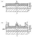
도 2는 도 1에 이어서, 제1 실시 형태에 따른 AlGaN/GaN·HEMT의 제조 방법을 공정순으로 도시하는 개략 단면도.
도 3은 도 2에 이어서, 제1 실시 형태에 따른 AlGaN/GaN·HEMT의 제조 방법을 공정순으로 도시하는 개략 단면도.
도 4는 도 3에 이어서, 제1 실시 형태에 따른 AlGaN/GaN·HEMT의 제조 방법을 공정순으로 도시하는 개략 단면도.
도 5는 제2 실시 형태에 따른 AlGaN/GaN·HEMT의 제조 방법의 주요 공정을 도시하는 개략 단면도.
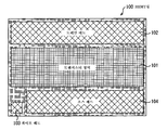
도 6은 제1 또는 제2 실시 형태에 따른 AlGaN/GaN·HEMT를 이용한 HEMT칩을 도시하는 개략 평면도.
도 7은 제1 또는 제2 실시 형태에 따른 AlGaN/GaN·HEMT를 이용한 HEMT칩의 디스크리트 패키지를 도시하는 개략 평면도.
도 8은 제3 실시 형태에 따른 PFC 회로를 도시하는 결선도.
도 9는 제4 실시 형태에 따른 전원 장치의 개략 구성을 도시하는 결선도.
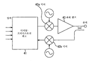
도 10은 제5 실시 형태에 따른 고주파 증폭기의 개략 구성을 도시하는 결선도.
2 : 화합물 반도체 적층 구조
2a : 핵 형성층
2b : 전자 주행층
2c : 중간층
2d : 전자 공급층
2e : 캡층
2eA, 2eB : 개구
3, 3a : MgO층
4 : 보호막
5 : Mg 확산 영역
6 : 소자 분리 구조
7 : 소스 전극
8 : 드레인 전극
9 : 게이트 절연막
20 : PFC 회로
21, 34a, 34b, 34c, 34d, 35a, 35b, 35c : 스위치 소자
22 : 다이오드
23 : 초크 코일
24, 25 : 컨덴서
26 : 다이오드 브릿지
30 : 풀 브릿지 인버터 회로
31 : 1차측 회로
32 : 2차측 회로
33 : 트랜스포머
41 : 디지털·프리디스토션 회로
42a, 42b : 믹서
43 : 파워 앰프
100 : HEMT칩
101 : 트랜지스터 영역
102 : 드레인 패드
103 : 게이트 패드
104 : 소스 패드
111 : 다이 어태치제
112 : 리드 프레임
112a : 드레인 리드
112b : 게이트 리드
112c : 소스 리드
113 : Al 와이어
114 : 몰드 수지
Claims (10)
- 화합물 반도체 적층 구조와,
상기 화합물 반도체 적층 구조의 상방에 형성된 전극
을 포함하고,
상기 화합물 반도체 적층 구조의 상기 전극에 위치 정합한 하방의 영역에서, 상기 화합물 반도체 적층 구조에 생성한 2차원 전자 가스의 일부를 소실시키는 깊이까지 p형 불순물이 국재(局在)하는 것을 특징으로 하는 화합물 반도체 장치. - 제1항에 있어서,
상기 화합물 반도체 적층 구조의 상기 전극에 위치 정합한 하방의 영역에서, 상기 화합물 반도체 적층 구조에 생성한 2차원 전자 가스의 일부를 소실시키는 깊이까지 상기 p형 불순물 및 산소가 국재하는 것을 특징으로 하는 화합물 반도체 장치. - 제1항 또는 제2항에 있어서,
상기 화합물 반도체 적층 구조와 상기 전극 사이에 형성된 절연막을 더 포함하는 것을 특징으로 하는 화합물 반도체 장치. - 제3항에 있어서,
상기 절연막은, 상기 p형 불순물의 열 확산원으로서 이용된, 상기 p형 불순물의 화합물층인 것을 특징으로 하는 화합물 반도체 장치. - 제1항 또는 제2항에 있어서,
상기 p형 불순물은, Mg 또는 Be인 것을 특징으로 하는 화합물 반도체 장치. - 화합물 반도체 적층 구조의 상방에 있어서의 전극 형성 영역에 p형 불순물의 화합물층을 형성하는 공정과,
상기 화합물층을 열처리하고, 상기 화합물 반도체 적층 구조에 생성한 2차원 전자 가스의 일부를 소실시키는 깊이까지, 상기 화합물층의 상기 p형 불순물을 확산시키는 공정
을 포함하는 것을 특징으로 하는 화합물 반도체 장치의 제조 방법. - 제6항에 있어서,
화합물 반도체 적층 구조의 상방을 덮도록 형성된 상기 화합물층을 웨트 에칭하고, 상기 화합물층을 상기 전극 형성 영역에 남기는 것을 특징으로 하는 화합물 반도체 장치의 제조 방법. - 제6항 또는 제7항에 있어서,
상기 화합물층을 덮도록 보호막을 형성하고, 상기 화합물층이 상기 보호막에 덮여진 상태에서 상기 열처리를 행하는 것을 특징으로 하는 화합물 반도체 장치의 제조 방법. - 제6항 또는 제7항에 있어서,
상기 열처리 후, 상기 화합물층을 제거하는 공정과,
상기 전극 형성 영역에 게이트 전극을 형성하는 공정
을 더 포함하는 것을 특징으로 하는 화합물 반도체 장치의 제조 방법. - 제6항 또는 제7항에 있어서,
상기 p형 불순물은, Mg 또는 Be인 것을 특징으로 하는 화합물 반도체 장치의 제조 방법.
Applications Claiming Priority (2)
| Application Number | Priority Date | Filing Date | Title |
|---|---|---|---|
| JPJP-P-2012-062708 | 2012-03-19 | ||
| JP2012062708A JP5902010B2 (ja) | 2012-03-19 | 2012-03-19 | 化合物半導体装置及びその製造方法 |
Publications (2)
| Publication Number | Publication Date |
|---|---|
| KR20130106263A true KR20130106263A (ko) | 2013-09-27 |
| KR101473534B1 KR101473534B1 (ko) | 2014-12-16 |
Family
ID=49157450
Family Applications (1)
| Application Number | Title | Priority Date | Filing Date |
|---|---|---|---|
| KR1020120153423A Active KR101473534B1 (ko) | 2012-03-19 | 2012-12-26 | 화합물 반도체 장치 및 그 제조 방법 |
Country Status (5)
| Country | Link |
|---|---|
| US (1) | US20130242618A1 (ko) |
| JP (1) | JP5902010B2 (ko) |
| KR (1) | KR101473534B1 (ko) |
| CN (1) | CN103325822B (ko) |
| TW (1) | TWI492378B (ko) |
Cited By (1)
| Publication number | Priority date | Publication date | Assignee | Title |
|---|---|---|---|---|
| CN103794643A (zh) * | 2014-01-22 | 2014-05-14 | 西安电子科技大学 | 一种基于槽栅高压器件及其制作方法 |
Families Citing this family (21)
| Publication number | Priority date | Publication date | Assignee | Title |
|---|---|---|---|---|
| JP6054620B2 (ja) * | 2012-03-29 | 2016-12-27 | トランスフォーム・ジャパン株式会社 | 化合物半導体装置及びその製造方法 |
| US9685345B2 (en) * | 2013-11-19 | 2017-06-20 | Nxp Usa, Inc. | Semiconductor devices with integrated Schottky diodes and methods of fabrication |
| WO2015166572A1 (ja) * | 2014-05-01 | 2015-11-05 | ルネサスエレクトロニクス株式会社 | 半導体装置および半導体装置の製造方法 |
| JP6308049B2 (ja) | 2014-06-26 | 2018-04-11 | 株式会社デンソー | 半導体装置の製造方法 |
| FR3026558B1 (fr) * | 2014-09-26 | 2018-03-09 | Commissariat A L'energie Atomique Et Aux Energies Alternatives | Procede d'activation de dopants dans une couche semi-conductrice a base de gan |
| CN106549049B (zh) * | 2015-09-17 | 2019-08-30 | 苏州能屋电子科技有限公司 | 一种电化学刻蚀p型氮化物实现增强型hemt的方法 |
| JP6560117B2 (ja) * | 2015-12-25 | 2019-08-14 | ルネサスエレクトロニクス株式会社 | 半導体装置の製造方法 |
| EP3751622A4 (en) * | 2018-02-06 | 2021-05-26 | Nissan Motor Co., Ltd. | SEMICONDUCTOR DEVICE |
| KR102060383B1 (ko) | 2018-02-23 | 2019-12-30 | 한국과학기술연구원 | 3족-5족 화합물 반도체 장치 |
| CN108807530B (zh) * | 2018-06-19 | 2021-02-09 | 深圳大学 | 异质结场效应晶体管及其制备方法 |
| US12142642B2 (en) * | 2018-06-20 | 2024-11-12 | Lawrence Livermore National Security, Llc | Field assisted interfacial diffusion doping through heterostructure design |
| US11101378B2 (en) | 2019-04-09 | 2021-08-24 | Raytheon Company | Semiconductor structure having both enhancement mode group III-N high electron mobility transistors and depletion mode group III-N high electron mobility transistors |
| US11258270B2 (en) * | 2019-06-28 | 2022-02-22 | Alpha And Omega Semiconductor (Cayman) Ltd. | Super-fast transient response (STR) AC/DC converter for high power density charging application |
| US10630080B1 (en) * | 2019-06-28 | 2020-04-21 | Alpha And Omega Semiconductor (Cayman) Ltd. | Super-fast transient response (STR) AC/DC Converter for high power density charging application |
| CN110911484B (zh) * | 2019-11-22 | 2021-02-19 | 华南理工大学 | 湿法腐蚀辅助掺杂制备的增强型GaN HEMT器件及制备方法 |
| US11545566B2 (en) | 2019-12-26 | 2023-01-03 | Raytheon Company | Gallium nitride high electron mobility transistors (HEMTs) having reduced current collapse and power added efficiency enhancement |
| US11881404B2 (en) * | 2020-02-11 | 2024-01-23 | QROMIS, Inc. | Method and system for diffusing magnesium in gallium nitride materials using sputtered magnesium sources |
| TWI767219B (zh) * | 2020-04-24 | 2022-06-11 | 環球晶圓股份有限公司 | 磊晶結構 |
| US11362190B2 (en) * | 2020-05-22 | 2022-06-14 | Raytheon Company | Depletion mode high electron mobility field effect transistor (HEMT) semiconductor device having beryllium doped Schottky contact layers |
| CN111681958A (zh) * | 2020-05-29 | 2020-09-18 | 华南理工大学 | 一种新型异质结构镁扩散制备常关型hemt器件的方法 |
| JP7534269B2 (ja) * | 2021-07-26 | 2024-08-14 | 株式会社東芝 | 半導体装置 |
Family Cites Families (12)
| Publication number | Priority date | Publication date | Assignee | Title |
|---|---|---|---|---|
| US6853018B2 (en) * | 2001-07-19 | 2005-02-08 | Sony Corporation | Semiconductor device having a channel layer, first semiconductor layer, second semiconductor layer, and a conductive impurity region |
| US8174048B2 (en) * | 2004-01-23 | 2012-05-08 | International Rectifier Corporation | III-nitride current control device and method of manufacture |
| JP2006032552A (ja) * | 2004-07-14 | 2006-02-02 | Toshiba Corp | 窒化物含有半導体装置 |
| JP2009038175A (ja) * | 2007-08-01 | 2009-02-19 | Panasonic Corp | 窒化物半導体トランジスタとその製造方法 |
| JP5384029B2 (ja) * | 2007-08-23 | 2014-01-08 | 日本碍子株式会社 | Misゲート構造型のhemt素子およびmisゲート構造型のhemt素子の作製方法 |
| EP2031653B1 (en) * | 2007-08-27 | 2014-03-05 | Denso Corporation | Manufacturing method for a semiconductor device having multiple element formation regions |
| JP4687742B2 (ja) * | 2007-08-27 | 2011-05-25 | 株式会社デンソー | 半導体装置の製造方法 |
| JP5487550B2 (ja) | 2007-08-29 | 2014-05-07 | サンケン電気株式会社 | 電界効果半導体装置及びその製造方法 |
| JP5487615B2 (ja) * | 2008-12-24 | 2014-05-07 | サンケン電気株式会社 | 電界効果半導体装置及びその製造方法 |
| JP2010245465A (ja) * | 2009-04-10 | 2010-10-28 | Mitsubishi Electric Corp | 窒化物系半導体レーザ及びその製造方法 |
| JP2011204717A (ja) * | 2010-03-24 | 2011-10-13 | Sanken Electric Co Ltd | 化合物半導体装置 |
| US9299821B2 (en) * | 2010-06-23 | 2016-03-29 | Cornell University | Gated III-V semiconductor structure and method |
-
2012
- 2012-03-19 JP JP2012062708A patent/JP5902010B2/ja not_active Expired - Fee Related
- 2012-12-18 TW TW101148014A patent/TWI492378B/zh active
- 2012-12-19 US US13/720,349 patent/US20130242618A1/en not_active Abandoned
- 2012-12-26 CN CN201210575487.7A patent/CN103325822B/zh active Active
- 2012-12-26 KR KR1020120153423A patent/KR101473534B1/ko active Active
Cited By (1)
| Publication number | Priority date | Publication date | Assignee | Title |
|---|---|---|---|---|
| CN103794643A (zh) * | 2014-01-22 | 2014-05-14 | 西安电子科技大学 | 一种基于槽栅高压器件及其制作方法 |
Also Published As
| Publication number | Publication date |
|---|---|
| TWI492378B (zh) | 2015-07-11 |
| JP2013197305A (ja) | 2013-09-30 |
| TW201340314A (zh) | 2013-10-01 |
| CN103325822B (zh) | 2016-03-30 |
| US20130242618A1 (en) | 2013-09-19 |
| KR101473534B1 (ko) | 2014-12-16 |
| CN103325822A (zh) | 2013-09-25 |
| JP5902010B2 (ja) | 2016-04-13 |
Similar Documents
| Publication | Publication Date | Title |
|---|---|---|
| JP5902010B2 (ja) | 化合物半導体装置及びその製造方法 | |
| JP6054621B2 (ja) | 化合物半導体装置及びその製造方法 | |
| TWI594431B (zh) | 化合物半導體裝置及其製造方法 | |
| JP6054620B2 (ja) | 化合物半導体装置及びその製造方法 | |
| JP5950643B2 (ja) | 化合物半導体装置及びその製造方法 | |
| JP5888064B2 (ja) | 化合物半導体装置及びその製造方法 | |
| JP5874173B2 (ja) | 化合物半導体装置及びその製造方法 | |
| JP5866773B2 (ja) | 化合物半導体装置及びその製造方法 | |
| KR101465306B1 (ko) | 화합물 반도체 장치 및 그 제조 방법 | |
| JP5908692B2 (ja) | 化合物半導体装置及びその製造方法 | |
| US9653569B1 (en) | Compound semiconductor device and manufacturing method thereof | |
| JP2014072397A (ja) | 化合物半導体装置及びその製造方法 | |
| JP7032641B2 (ja) | 化合物半導体装置及びその製造方法 | |
| JP2014090033A (ja) | 化合物半導体装置及びその製造方法 | |
| JP2014197644A (ja) | 化合物半導体装置及びその製造方法 |
Legal Events
| Date | Code | Title | Description |
|---|---|---|---|
| A201 | Request for examination | ||
| PA0109 | Patent application |
St.27 status event code: A-0-1-A10-A12-nap-PA0109 |
|
| PA0201 | Request for examination |
St.27 status event code: A-1-2-D10-D11-exm-PA0201 |
|
| D13-X000 | Search requested |
St.27 status event code: A-1-2-D10-D13-srh-X000 |
|
| PG1501 | Laying open of application |
St.27 status event code: A-1-1-Q10-Q12-nap-PG1501 |
|
| D14-X000 | Search report completed |
St.27 status event code: A-1-2-D10-D14-srh-X000 |
|
| E902 | Notification of reason for refusal | ||
| PE0902 | Notice of grounds for rejection |
St.27 status event code: A-1-2-D10-D21-exm-PE0902 |
|
| P11-X000 | Amendment of application requested |
St.27 status event code: A-2-2-P10-P11-nap-X000 |
|
| P13-X000 | Application amended |
St.27 status event code: A-2-2-P10-P13-nap-X000 |
|
| N231 | Notification of change of applicant | ||
| PN2301 | Change of applicant |
St.27 status event code: A-3-3-R10-R13-asn-PN2301 St.27 status event code: A-3-3-R10-R11-asn-PN2301 |
|
| E902 | Notification of reason for refusal | ||
| PE0902 | Notice of grounds for rejection |
St.27 status event code: A-1-2-D10-D21-exm-PE0902 |
|
| T11-X000 | Administrative time limit extension requested |
St.27 status event code: U-3-3-T10-T11-oth-X000 |
|
| P11-X000 | Amendment of application requested |
St.27 status event code: A-2-2-P10-P11-nap-X000 |
|
| P13-X000 | Application amended |
St.27 status event code: A-2-2-P10-P13-nap-X000 |
|
| E701 | Decision to grant or registration of patent right | ||
| PE0701 | Decision of registration |
St.27 status event code: A-1-2-D10-D22-exm-PE0701 |
|
| GRNT | Written decision to grant | ||
| PR0701 | Registration of establishment |
St.27 status event code: A-2-4-F10-F11-exm-PR0701 |
|
| PR1002 | Payment of registration fee |
St.27 status event code: A-2-2-U10-U11-oth-PR1002 Fee payment year number: 1 |
|
| PG1601 | Publication of registration |
St.27 status event code: A-4-4-Q10-Q13-nap-PG1601 |
|
| FPAY | Annual fee payment |
Payment date: 20171201 Year of fee payment: 4 |
|
| PR1001 | Payment of annual fee |
St.27 status event code: A-4-4-U10-U11-oth-PR1001 Fee payment year number: 4 |
|
| PR1001 | Payment of annual fee |
St.27 status event code: A-4-4-U10-U11-oth-PR1001 Fee payment year number: 5 |
|
| PR1001 | Payment of annual fee |
St.27 status event code: A-4-4-U10-U11-oth-PR1001 Fee payment year number: 6 |
|
| PR1001 | Payment of annual fee |
St.27 status event code: A-4-4-U10-U11-oth-PR1001 Fee payment year number: 7 |
|
| PR1001 | Payment of annual fee |
St.27 status event code: A-4-4-U10-U11-oth-PR1001 Fee payment year number: 8 |
|
| PR1001 | Payment of annual fee |
St.27 status event code: A-4-4-U10-U11-oth-PR1001 Fee payment year number: 9 |
|
| PR1001 | Payment of annual fee |
St.27 status event code: A-4-4-U10-U11-oth-PR1001 Fee payment year number: 10 |
|
| PR1001 | Payment of annual fee |
St.27 status event code: A-4-4-U10-U11-oth-PR1001 Fee payment year number: 11 |
|
| P22-X000 | Classification modified |
St.27 status event code: A-4-4-P10-P22-nap-X000 |
|
| P22-X000 | Classification modified |
St.27 status event code: A-4-4-P10-P22-nap-X000 |