KR20130107588A - Mos 트랜지스터의 형성 방법 - Google Patents
Mos 트랜지스터의 형성 방법 Download PDFInfo
- Publication number
- KR20130107588A KR20130107588A KR1020120029492A KR20120029492A KR20130107588A KR 20130107588 A KR20130107588 A KR 20130107588A KR 1020120029492 A KR1020120029492 A KR 1020120029492A KR 20120029492 A KR20120029492 A KR 20120029492A KR 20130107588 A KR20130107588 A KR 20130107588A
- Authority
- KR
- South Korea
- Prior art keywords
- spacer
- spacer layer
- gate structure
- gate
- source
- Prior art date
- Legal status (The legal status is an assumption and is not a legal conclusion. Google has not performed a legal analysis and makes no representation as to the accuracy of the status listed.)
- Ceased
Links
Images












Classifications
-
- H—ELECTRICITY
- H10—SEMICONDUCTOR DEVICES; ELECTRIC SOLID-STATE DEVICES NOT OTHERWISE PROVIDED FOR
- H10D—INORGANIC ELECTRIC SEMICONDUCTOR DEVICES
- H10D30/00—Field-effect transistors [FET]
- H10D30/60—Insulated-gate field-effect transistors [IGFET]
-
- H—ELECTRICITY
- H10—SEMICONDUCTOR DEVICES; ELECTRIC SOLID-STATE DEVICES NOT OTHERWISE PROVIDED FOR
- H10D—INORGANIC ELECTRIC SEMICONDUCTOR DEVICES
- H10D64/00—Electrodes of devices having potential barriers
- H10D64/01—Manufacture or treatment
- H10D64/021—Manufacture or treatment using multiple gate spacer layers, e.g. bilayered sidewall spacers
-
- H—ELECTRICITY
- H10—SEMICONDUCTOR DEVICES; ELECTRIC SOLID-STATE DEVICES NOT OTHERWISE PROVIDED FOR
- H10D—INORGANIC ELECTRIC SEMICONDUCTOR DEVICES
- H10D30/00—Field-effect transistors [FET]
- H10D30/01—Manufacture or treatment
- H10D30/021—Manufacture or treatment of FETs having insulated gates [IGFET]
- H10D30/0223—Manufacture or treatment of FETs having insulated gates [IGFET] having source and drain regions or source and drain extensions self-aligned to sides of the gate
- H10D30/0227—Manufacture or treatment of FETs having insulated gates [IGFET] having source and drain regions or source and drain extensions self-aligned to sides of the gate having both lightly-doped source and drain extensions and source and drain regions self-aligned to the sides of the gate, e.g. lightly-doped drain [LDD] MOSFET or double-diffused drain [DDD] MOSFET
-
- H—ELECTRICITY
- H10—SEMICONDUCTOR DEVICES; ELECTRIC SOLID-STATE DEVICES NOT OTHERWISE PROVIDED FOR
- H10D—INORGANIC ELECTRIC SEMICONDUCTOR DEVICES
- H10D30/00—Field-effect transistors [FET]
- H10D30/60—Insulated-gate field-effect transistors [IGFET]
- H10D30/601—Insulated-gate field-effect transistors [IGFET] having lightly-doped drain or source extensions, e.g. LDD IGFETs or DDD IGFETs
-
- H—ELECTRICITY
- H10—SEMICONDUCTOR DEVICES; ELECTRIC SOLID-STATE DEVICES NOT OTHERWISE PROVIDED FOR
- H10D—INORGANIC ELECTRIC SEMICONDUCTOR DEVICES
- H10D84/00—Integrated devices formed in or on semiconductor substrates that comprise only semiconducting layers, e.g. on Si wafers or on GaAs-on-Si wafers
- H10D84/01—Manufacture or treatment
- H10D84/0123—Integrating together multiple components covered by H10D12/00 or H10D30/00, e.g. integrating multiple IGBTs
- H10D84/0126—Integrating together multiple components covered by H10D12/00 or H10D30/00, e.g. integrating multiple IGBTs the components including insulated gates, e.g. IGFETs
- H10D84/0165—Integrating together multiple components covered by H10D12/00 or H10D30/00, e.g. integrating multiple IGBTs the components including insulated gates, e.g. IGFETs the components including complementary IGFETs, e.g. CMOS devices
- H10D84/0184—Manufacturing their gate sidewall spacers
-
- H—ELECTRICITY
- H10—SEMICONDUCTOR DEVICES; ELECTRIC SOLID-STATE DEVICES NOT OTHERWISE PROVIDED FOR
- H10D—INORGANIC ELECTRIC SEMICONDUCTOR DEVICES
- H10D84/00—Integrated devices formed in or on semiconductor substrates that comprise only semiconducting layers, e.g. on Si wafers or on GaAs-on-Si wafers
- H10D84/01—Manufacture or treatment
- H10D84/02—Manufacture or treatment characterised by using material-based technologies
- H10D84/03—Manufacture or treatment characterised by using material-based technologies using Group IV technology, e.g. silicon technology or silicon-carbide [SiC] technology
- H10D84/038—Manufacture or treatment characterised by using material-based technologies using Group IV technology, e.g. silicon technology or silicon-carbide [SiC] technology using silicon technology, e.g. SiGe
Landscapes
- Insulated Gate Type Field-Effect Transistor (AREA)
Abstract
Description
도 1b는 도 1a의 변형된 예에 따른 MOS 트랜지스터를 나타내는 단면도이다.
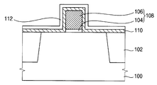
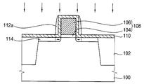
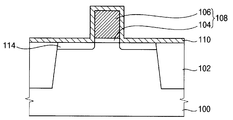
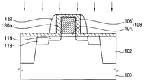
도 2a 내지 도 2g는 도 1a에 도시된 트랜지스터의 제조 방법을 나타내는 단면도들이다.
도 3a는 본 발명의 실시예 2에 따른 MOS 트랜지스터를 나타내는 단면도이다.
도 3b는 도 3a의 변형된 예에 따른 MOS 트랜지스터를 나타내는 단면도이다.
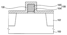
도 4a 내지 도 4c는 도 3a에 도시된 트랜지스터의 제조 방법을 나타내는 단면도들이다.
도 5a는 본 발명의 실시예 3에 따른 MOS 트랜지스터를 나타내는 단면도이다.
도 5b는 도 5a의 변형된 예에 따른 MOS 트랜지스터를 나타내는 단면도이다.
도 6a 내지 도 6d는 도 5a에 도시된 트랜지스터의 제조 방법을 나타내는 단면도들이다.
도 7은 본 발명의 실시예 4에 따른 CMOS 트랜지스터를 나타내는 단면도이다.
도 8a 내지 도 8e는 도 7에 도시된 CMOS 트랜지스터의 제조 방법을 나타내는 단면도들이다.
도 9a 내지 도 9c는 도 7에 도시된 CMOS 트랜지스터의 다른 형성 방법을 나타내는 단면도들이다.
도 10은 1군 샘플 및 1군 비교 샘플들의 게이트 길이별 문턱 전압을 나타내는 그래프이다.
도 11은 샘플1 및 비교 샘플1에서의 각 게이트 전압별 바디 오프 전류를 나타내는 그래프이다.
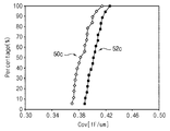
도 12는 샘플2 및 비교 샘플2에서의 오버랩 커패시턴스를 나타내는 그래프이다.
도 13은 샘플2 및 비교 샘플2에서의 오프 전류 및 온 전류(포화 드레인 전류, Idsat)를 나타내는 그래프이다.
110 : 제1 스페이서막 112 : 제2 스페이서막
112a : 제2 스페이서 114 : 소오스/드레인 확장 영역
116 : 제3 스페이서 118 : 소오스/드레인 영역
120 : 제3 스페이서 130 : 예비 제1 스페이서막
130a : 제1 스페이서막 132 : 제2 스페이서
Claims (10)
- 반도체 기판에 게이트 산화막 패턴 및 게이트 전극이 적층된 게이트 구조물을 형성하는 단계;
상기 반도체 기판 및 게이트 구조물의 표면 상에 컨포멀하게 제1 스페이서막을 형성하는 단계;
상기 제1 스페이서막 상에 제2 스페이서막을 형성하는 단계;
상기 제2 스페이서막을 이방성 식각하여, 상기 게이트 구조물 측벽에 위치하는 제1 스페이서막 상에 제2 스페이서를 형성하는 단계; 및
상기 게이트 구조물 및 상기 게이트 구조물 측벽 상의 제1 스페이서막 및 제2 스페이서를 이용하여 상기 반도체 기판에 불순물을 이온주입하여 소오스/드레인 확장 영역을 형성하는 단계를 포함하는 MOS 트랜지스터의 형성 방법. - 제1항에 있어서, 상기 제1 및 제2 스페이서막은 절연 물질을 포함하고, 서로 식각 선택비를 갖는 물질로 형성되는 MOS 트랜지스터의 형성 방법.
- 제1항에 있어서, 상기 제1 스페이서막은 실리콘 질화물을 포함하고, 상기 제2 스페이서막은 실리콘 산화물을 포함하는 MOS 트랜지스터의 형성 방법.
- 제1항에 있어서, 상기 게이트 구조물 측벽 상의 제1 스페이서막 및 제2 스페이서의 두께 합은 상기 불순물의 확산되는 거리가 증가될수록 더 두껍게 형성하는 MOS 트랜지스터의 형성 방법.
- 제1항에 있어서, 상기 게이트 구조물 측벽 상의 제1 스페이서막 및 제2 스페이서의 두께 합은 상기 제2 스페이서의 증착 두께에 의해 조절하는 MOS 트랜지스터의 형성 방법.
- 제1항에 있어서, 상기 제1 스페이서막은 20 내지 50Å의 두께를 갖도록 형성하는 MOS 트랜지스터의 형성 방법.
- 제1항에 있어서, 상기 제2 스페이서는 10 내지 50Å의 두께를 갖도록 형성하는 MOS 트랜지스터의 형성 방법.
- 제1항에 있어서, 상기 게이트 구조물의 선폭이 10 내지 30㎚가 되도록 상기 게이트 구조물을 패터닝하는 MOS 트랜지스터의 형성 방법.
- 제1항에 있어서, 상기 소오스/드레인 확장 영역을 형성한 다음, 상기 제2 스페이서를 제거하는 단계를 더 포함하는 MOS 트랜지스터의 형성 방법.
- 제1항에 있어서, 상기 소오스/드레인 확장 영역을 형성한 다음,
상기 제1 스페이서막 및 제2 스페이서 상에 제3 스페이서막을 형성하는 단계;
상기 제3 스페이서막을 이방성 식각하여 제3 스페이서를 형성하는 단계; 및
상기 제3 스페이서가 형성된 게이트 구조물을 이용하여 상기 기판에 상기 반도체 기판에 불순물을 이온주입하여 소오스/드레인 영역을 형성하는 단계를 포함하는 MOS 트랜지스터의 형성 방법.
Priority Applications (2)
| Application Number | Priority Date | Filing Date | Title |
|---|---|---|---|
| KR1020120029492A KR20130107588A (ko) | 2012-03-22 | 2012-03-22 | Mos 트랜지스터의 형성 방법 |
| US13/687,104 US8753945B2 (en) | 2012-03-22 | 2012-11-28 | Method of manufacturing a semiconductor device |
Applications Claiming Priority (1)
| Application Number | Priority Date | Filing Date | Title |
|---|---|---|---|
| KR1020120029492A KR20130107588A (ko) | 2012-03-22 | 2012-03-22 | Mos 트랜지스터의 형성 방법 |
Publications (1)
| Publication Number | Publication Date |
|---|---|
| KR20130107588A true KR20130107588A (ko) | 2013-10-02 |
Family
ID=49212208
Family Applications (1)
| Application Number | Title | Priority Date | Filing Date |
|---|---|---|---|
| KR1020120029492A Ceased KR20130107588A (ko) | 2012-03-22 | 2012-03-22 | Mos 트랜지스터의 형성 방법 |
Country Status (2)
| Country | Link |
|---|---|
| US (1) | US8753945B2 (ko) |
| KR (1) | KR20130107588A (ko) |
Families Citing this family (4)
| Publication number | Priority date | Publication date | Assignee | Title |
|---|---|---|---|---|
| US9196708B2 (en) * | 2013-12-30 | 2015-11-24 | Taiwan Semiconductor Manufacturing Co., Ltd | Method for forming a semiconductor device structure |
| US9935013B2 (en) | 2014-04-09 | 2018-04-03 | Taiwan Semiconductor Manufacturing Co., Ltd. | Flexible device modulation by oxide isolation structure selective etching process |
| US11653498B2 (en) * | 2017-11-30 | 2023-05-16 | Taiwan Semiconductor Manufacturing Co., Ltd. | Memory device with improved data retention |
| US20220238711A1 (en) * | 2021-01-27 | 2022-07-28 | Micron Technology, Inc. | Semiconductor device having mos transistor for efficient stress transfer |
Citations (2)
| Publication number | Priority date | Publication date | Assignee | Title |
|---|---|---|---|---|
| US20050095796A1 (en) * | 2003-10-31 | 2005-05-05 | Van Bentum Ralf | Technique for forming a transistor having raised drain and source regions with a reduced number of process steps |
| US20090032888A1 (en) * | 2004-10-20 | 2009-02-05 | Advanced Micro Devices, Inc. | Semiconductor device |
Family Cites Families (8)
| Publication number | Priority date | Publication date | Assignee | Title |
|---|---|---|---|---|
| US5677224A (en) * | 1996-09-03 | 1997-10-14 | Advanced Micro Devices, Inc. | Method of making asymmetrical N-channel and P-channel devices |
| JPH10256247A (ja) | 1997-03-12 | 1998-09-25 | Toshiba Microelectron Corp | 半導体装置製造方法 |
| JP2000114522A (ja) | 1998-10-08 | 2000-04-21 | Toshiba Corp | 半導体装置及びその製造方法 |
| US6071826A (en) | 1999-02-12 | 2000-06-06 | Taiwan Semiconductor Manufacturing Company | Method of manufacturing CMOS image sensor leakage free with double layer spacer |
| US20050275034A1 (en) | 2004-04-08 | 2005-12-15 | International Business Machines Corporation | A manufacturable method and structure for double spacer cmos with optimized nfet/pfet performance |
| KR20060000322A (ko) | 2004-06-28 | 2006-01-06 | (주)그래픽테크노재팬 | Cmos 이미지 센서 및 그 제조방법 |
| TW200849556A (en) | 2006-06-14 | 2008-12-16 | Nxp Bv | Semiconductor device and method of manufacturing such a device |
| US20090166625A1 (en) | 2007-12-28 | 2009-07-02 | United Microelectronics Corp. | Mos device structure |
-
2012
- 2012-03-22 KR KR1020120029492A patent/KR20130107588A/ko not_active Ceased
- 2012-11-28 US US13/687,104 patent/US8753945B2/en active Active
Patent Citations (2)
| Publication number | Priority date | Publication date | Assignee | Title |
|---|---|---|---|---|
| US20050095796A1 (en) * | 2003-10-31 | 2005-05-05 | Van Bentum Ralf | Technique for forming a transistor having raised drain and source regions with a reduced number of process steps |
| US20090032888A1 (en) * | 2004-10-20 | 2009-02-05 | Advanced Micro Devices, Inc. | Semiconductor device |
Also Published As
| Publication number | Publication date |
|---|---|
| US8753945B2 (en) | 2014-06-17 |
| US20130252393A1 (en) | 2013-09-26 |
Similar Documents
| Publication | Publication Date | Title |
|---|---|---|
| CN100369208C (zh) | 在半导体装置的多栅极晶体管上形成栅极电极的方法 | |
| US7888734B2 (en) | High-voltage MOS devices having gates extending into recesses of substrates | |
| KR101547707B1 (ko) | 비대칭 전계 효과 트랜지스터들을 제조하는 방법 | |
| EP2230686B1 (en) | Method of manufacturing semiconductor device | |
| US8216908B2 (en) | Extended drain transistor and method of manufacturing the same | |
| KR20190087786A (ko) | 반도체 소자 및 그 제조 방법 | |
| US20120267724A1 (en) | Mos semiconductor device and methods for its fabrication | |
| KR102449211B1 (ko) | 전계 효과 트랜지스터를 포함하는 반도체 소자 | |
| US7569480B2 (en) | Semiconductor devices and methods of fabricating the same | |
| KR20130107588A (ko) | Mos 트랜지스터의 형성 방법 | |
| JP2005136258A (ja) | 半導体装置およびその製造方法 | |
| CN101542737B (zh) | 自对准碰撞电离场效应晶体管 | |
| CN103247528B (zh) | 金属氧化物半导体场效应管的制造方法 | |
| CN108666221B (zh) | 半导体结构及其形成方法 | |
| US7863692B2 (en) | Semiconductor device | |
| US8841728B2 (en) | Semiconductor device and method of manufacturing the same | |
| US7915128B2 (en) | High voltage semiconductor devices | |
| US6680504B2 (en) | Method for constructing a metal oxide semiconductor field effect transistor | |
| KR100906557B1 (ko) | 반도체소자 및 그 제조방법 | |
| US20170263770A1 (en) | Semiconductor device and manufacturing method of the same | |
| KR20150097946A (ko) | 반도체 소자의 제조 방법 | |
| TW201523881A (zh) | 終止區結構及其製造方法 | |
| CN116153972B (zh) | 一种半导体装置及其制造方法 | |
| US7727829B2 (en) | Method of forming a semiconductor device having a removable sidewall spacer | |
| US6905932B2 (en) | Method for constructing a metal oxide semiconductor field effect transistor |
Legal Events
| Date | Code | Title | Description |
|---|---|---|---|
| PA0109 | Patent application |
Patent event code: PA01091R01D Comment text: Patent Application Patent event date: 20120322 |
|
| PG1501 | Laying open of application | ||
| A201 | Request for examination | ||
| PA0201 | Request for examination |
Patent event code: PA02012R01D Patent event date: 20170313 Comment text: Request for Examination of Application Patent event code: PA02011R01I Patent event date: 20120322 Comment text: Patent Application |
|
| E902 | Notification of reason for refusal | ||
| PE0902 | Notice of grounds for rejection |
Comment text: Notification of reason for refusal Patent event date: 20180209 Patent event code: PE09021S01D |
|
| E601 | Decision to refuse application | ||
| PE0601 | Decision on rejection of patent |
Patent event date: 20180828 Comment text: Decision to Refuse Application Patent event code: PE06012S01D Patent event date: 20180209 Comment text: Notification of reason for refusal Patent event code: PE06011S01I |