KR20130110491A - 액정표시장치 - Google Patents
액정표시장치 Download PDFInfo
- Publication number
- KR20130110491A KR20130110491A KR1020120032513A KR20120032513A KR20130110491A KR 20130110491 A KR20130110491 A KR 20130110491A KR 1020120032513 A KR1020120032513 A KR 1020120032513A KR 20120032513 A KR20120032513 A KR 20120032513A KR 20130110491 A KR20130110491 A KR 20130110491A
- Authority
- KR
- South Korea
- Prior art keywords
- liquid crystal
- crystal display
- circuit board
- main circuit
- light source
- Prior art date
- Legal status (The legal status is an assumption and is not a legal conclusion. Google has not performed a legal analysis and makes no representation as to the accuracy of the status listed.)
- Ceased
Links
Images




Classifications
-
- G—PHYSICS
- G02—OPTICS
- G02F—OPTICAL DEVICES OR ARRANGEMENTS FOR THE CONTROL OF LIGHT BY MODIFICATION OF THE OPTICAL PROPERTIES OF THE MEDIA OF THE ELEMENTS INVOLVED THEREIN; NON-LINEAR OPTICS; FREQUENCY-CHANGING OF LIGHT; OPTICAL LOGIC ELEMENTS; OPTICAL ANALOGUE/DIGITAL CONVERTERS
- G02F1/00—Devices or arrangements for the control of the intensity, colour, phase, polarisation or direction of light arriving from an independent light source, e.g. switching, gating or modulating; Non-linear optics
- G02F1/01—Devices or arrangements for the control of the intensity, colour, phase, polarisation or direction of light arriving from an independent light source, e.g. switching, gating or modulating; Non-linear optics for the control of the intensity, phase, polarisation or colour
- G02F1/13—Devices or arrangements for the control of the intensity, colour, phase, polarisation or direction of light arriving from an independent light source, e.g. switching, gating or modulating; Non-linear optics for the control of the intensity, phase, polarisation or colour based on liquid crystals, e.g. single liquid crystal display cells
- G02F1/133—Constructional arrangements; Operation of liquid crystal cells; Circuit arrangements
- G02F1/1333—Constructional arrangements; Manufacturing methods
- G02F1/133308—Support structures for LCD panels, e.g. frames or bezels
-
- G—PHYSICS
- G02—OPTICS
- G02F—OPTICAL DEVICES OR ARRANGEMENTS FOR THE CONTROL OF LIGHT BY MODIFICATION OF THE OPTICAL PROPERTIES OF THE MEDIA OF THE ELEMENTS INVOLVED THEREIN; NON-LINEAR OPTICS; FREQUENCY-CHANGING OF LIGHT; OPTICAL LOGIC ELEMENTS; OPTICAL ANALOGUE/DIGITAL CONVERTERS
- G02F1/00—Devices or arrangements for the control of the intensity, colour, phase, polarisation or direction of light arriving from an independent light source, e.g. switching, gating or modulating; Non-linear optics
- G02F1/01—Devices or arrangements for the control of the intensity, colour, phase, polarisation or direction of light arriving from an independent light source, e.g. switching, gating or modulating; Non-linear optics for the control of the intensity, phase, polarisation or colour
- G02F1/13—Devices or arrangements for the control of the intensity, colour, phase, polarisation or direction of light arriving from an independent light source, e.g. switching, gating or modulating; Non-linear optics for the control of the intensity, phase, polarisation or colour based on liquid crystals, e.g. single liquid crystal display cells
- G02F1/133—Constructional arrangements; Operation of liquid crystal cells; Circuit arrangements
- G02F1/1333—Constructional arrangements; Manufacturing methods
-
- G—PHYSICS
- G02—OPTICS
- G02F—OPTICAL DEVICES OR ARRANGEMENTS FOR THE CONTROL OF LIGHT BY MODIFICATION OF THE OPTICAL PROPERTIES OF THE MEDIA OF THE ELEMENTS INVOLVED THEREIN; NON-LINEAR OPTICS; FREQUENCY-CHANGING OF LIGHT; OPTICAL LOGIC ELEMENTS; OPTICAL ANALOGUE/DIGITAL CONVERTERS
- G02F1/00—Devices or arrangements for the control of the intensity, colour, phase, polarisation or direction of light arriving from an independent light source, e.g. switching, gating or modulating; Non-linear optics
- G02F1/01—Devices or arrangements for the control of the intensity, colour, phase, polarisation or direction of light arriving from an independent light source, e.g. switching, gating or modulating; Non-linear optics for the control of the intensity, phase, polarisation or colour
- G02F1/13—Devices or arrangements for the control of the intensity, colour, phase, polarisation or direction of light arriving from an independent light source, e.g. switching, gating or modulating; Non-linear optics for the control of the intensity, phase, polarisation or colour based on liquid crystals, e.g. single liquid crystal display cells
- G02F1/133—Constructional arrangements; Operation of liquid crystal cells; Circuit arrangements
- G02F1/1333—Constructional arrangements; Manufacturing methods
- G02F1/133342—Constructional arrangements; Manufacturing methods for double-sided displays
-
- G—PHYSICS
- G02—OPTICS
- G02F—OPTICAL DEVICES OR ARRANGEMENTS FOR THE CONTROL OF LIGHT BY MODIFICATION OF THE OPTICAL PROPERTIES OF THE MEDIA OF THE ELEMENTS INVOLVED THEREIN; NON-LINEAR OPTICS; FREQUENCY-CHANGING OF LIGHT; OPTICAL LOGIC ELEMENTS; OPTICAL ANALOGUE/DIGITAL CONVERTERS
- G02F1/00—Devices or arrangements for the control of the intensity, colour, phase, polarisation or direction of light arriving from an independent light source, e.g. switching, gating or modulating; Non-linear optics
- G02F1/01—Devices or arrangements for the control of the intensity, colour, phase, polarisation or direction of light arriving from an independent light source, e.g. switching, gating or modulating; Non-linear optics for the control of the intensity, phase, polarisation or colour
- G02F1/13—Devices or arrangements for the control of the intensity, colour, phase, polarisation or direction of light arriving from an independent light source, e.g. switching, gating or modulating; Non-linear optics for the control of the intensity, phase, polarisation or colour based on liquid crystals, e.g. single liquid crystal display cells
- G02F1/133—Constructional arrangements; Operation of liquid crystal cells; Circuit arrangements
- G02F1/1333—Constructional arrangements; Manufacturing methods
- G02F1/1335—Structural association of cells with optical devices, e.g. polarisers or reflectors
- G02F1/1336—Illuminating devices
- G02F1/133615—Edge-illuminating devices, i.e. illuminating from the side
-
- G—PHYSICS
- G02—OPTICS
- G02F—OPTICAL DEVICES OR ARRANGEMENTS FOR THE CONTROL OF LIGHT BY MODIFICATION OF THE OPTICAL PROPERTIES OF THE MEDIA OF THE ELEMENTS INVOLVED THEREIN; NON-LINEAR OPTICS; FREQUENCY-CHANGING OF LIGHT; OPTICAL LOGIC ELEMENTS; OPTICAL ANALOGUE/DIGITAL CONVERTERS
- G02F1/00—Devices or arrangements for the control of the intensity, colour, phase, polarisation or direction of light arriving from an independent light source, e.g. switching, gating or modulating; Non-linear optics
- G02F1/01—Devices or arrangements for the control of the intensity, colour, phase, polarisation or direction of light arriving from an independent light source, e.g. switching, gating or modulating; Non-linear optics for the control of the intensity, phase, polarisation or colour
- G02F1/13—Devices or arrangements for the control of the intensity, colour, phase, polarisation or direction of light arriving from an independent light source, e.g. switching, gating or modulating; Non-linear optics for the control of the intensity, phase, polarisation or colour based on liquid crystals, e.g. single liquid crystal display cells
- G02F1/133—Constructional arrangements; Operation of liquid crystal cells; Circuit arrangements
- G02F1/1333—Constructional arrangements; Manufacturing methods
- G02F1/1335—Structural association of cells with optical devices, e.g. polarisers or reflectors
- G02F1/1336—Illuminating devices
- G02F1/133628—Illuminating devices with cooling means
Landscapes
- Physics & Mathematics (AREA)
- Nonlinear Science (AREA)
- Mathematical Physics (AREA)
- Chemical & Material Sciences (AREA)
- Crystallography & Structural Chemistry (AREA)
- General Physics & Mathematics (AREA)
- Optics & Photonics (AREA)
- Liquid Crystal (AREA)
Abstract
Description
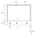
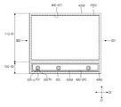
도 2는 도 1에 도시된 액정표시장치의 상면도이다.
도 3은 도 2의 Ⅰ-Ⅰ'를 따라 절단한 단면도이다.
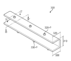
도 4a는 도 1에 도시된 방열부재의 사시도이다.
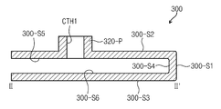
도 4b은 도 4a의 Ⅱ-Ⅱ'를 따라 절단한 단면도이다.
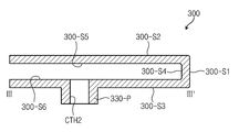
도 4c은 도 4a의 Ⅲ-Ⅲ'를 따라 절단한 단면도이다.
도 5는 도 1에 도시된 액정표시장치에 있어서, 보호 프레임이 제거된 상태의 상면도이다.
도 6a 및 도 6b는 도 5에 도시된 액정표시장치의 측면도이다.
도 7은 도 6b의 일부분을 확대한 도면이다.
300: 방열부재 400U, 400L: 지지부재
500U, 500L: 메인회로기판 600U, 600L: 액정표시패널
700U, 700L: 보호부재
Claims (19)
- 제1 출사면, 상기 제1 출사면에 마주하는 제2 출사면, 및 상기 제1 출사면과 상기 제2 출사면을 연결하는 복수 개의 측면들을 구비한 도광판;
상기 복수 개의 측면들 중 적어도 어느 하나에 마주하며, 상기 적어도 어느 하나의 측면에 광을 제공하는 광원;
상기 제1 출사면을 통해 출사된 광을 수신하여 이미지를 생성하는 제1 액정표시패널;
상기 제2 출사면을 통해 출사된 광을 수신하여 이미지를 생성하는 제2 액정표시패널;
상기 제1 액정표시패널에 전기적 신호를 제공하는 제1 메인회로기판;
상기 제2 액정표시패널에 전기적 신호를 제공하는 제2 메인회로기판; 및
상기 광원, 상기 제1 메인회로기판, 및 상기 제2 메인회로기판을 실장하며, 상기 광원, 상기 제1 메인회로기판, 및 상기 제2 메인회로기판에서 발생한 열을 방출하는 방열부재를 포함하는 액정표시장치. - 제1 항에 있어서,
상기 방열부재는 상기 광원에 마주하는 제1 표면, 상기 제1 표면으로부터 절곡된 제2 표면, 상기 제1 표면으로부터 상기 제2 표면과 다른 방향으로 절곡된 제3 표면을 구비하고,
상기 광원은 상기 제1 표면 상에 실장되고, 상기 제1 메인회로기판은 상기 제2 표면 상에 실장되며, 상기 제2 메인회로기판은 상기 제3 표면 상에 실장된 것을 특징으로 하는 액정표시장치. - 제2 항에 있어서,
상기 제1 표면은 상기 복수 개의 측면들 중 상기 적어도 어느 하나의 측면과 실질적으로 평행하고, 상기 제2 표면은 상기 제1 출사면과 실질적으로 평행하며, 상기 제3 표면은 상기 제2 출사면과 실질적으로 평행한 것을 특징으로 하는 액정표시장치. - 제2 항에 있어서,
상기 광원은 복수 개의 발광소자들 및 상기 복수 개의 발광소자들을 실장하는 광원용 회로기판을 포함하고,
상기 광원용 회로기판은 상기 제1 표면 상에 실장되는 것을 특징으로 하는 액정표시장치. - 제4 항에 있어서,
상기 방열부재와 상기 광원용 회로기판은 상기 제 1 표면과 상기 광원용 회로기판의 일면 사이에 구비된 열전달 접착부재에 의해서 접착되며, 상시 열전달 접착부재는 상기 광원용 회로기판에서 발생한 열을 상기 방열부재에 전달하는 것을 특징으로 하는 액정표시장치. - 제2 항에 있어서,
상기 방열부재는 상기 제1 표면을 구비한 수직부, 상기 수직부으로부터 절곡되고 상기 제2 표면을 구비한 제1 수평부, 및 상기 수직부으로부터 절곡되고 상기 제3 표면을 구비한 제2 수평부를 포함하는 것을 특징으로 하는 액정표시장치. - 제6 항에 있어서,
상기 제1 수평부과 상기 제2 수평부는 서로 이격되어 배치되고, 서로 마주하는 것을 특징으로 하는 액정표시장치. - 제6 항에 있어서,
상기 제1 액정표시패널의 일부분을 커버하는 제1 영역 및 상기 제1 메인회로기판을 커버하는 제2 영역을 구비하는 제1 보호부재; 및
상기 제2 액정표시패널의 일부분을 커버하는 제1 영역 및 상기 제2 메인회로기판을 커버하는 제2 영역을 구비하고, 상기 제1 보호부재와 결합하는 제2 보호부재를 더 포함하는 것을 특징으로 액정표시장치. - 제8 항에 있어서,
상기 제1 메인회로기판 및 상기 제2 메인회로기판은 적어도 하나의 제1 관통홀을 각각 포함하고,
상기 방열부재는 상기 제1 메인회로기판의 상기 적어도 하나의 제1 관통홀에 삽입되는 적어도 하나의 제1 돌출부 및 상기 제2 메인회로기판의 상기 적어도 하나의 제1 관통홀에 삽입되는 적어도 하나의 제2 돌출부를 더 포함하는 것을 특징으로 하는 액정표시장치. - 제9 항에 있어서,
상기 방열부재는 상기 적어도 하나의 제1 돌출부의 길이 방향으로 상기 적어도 하나의 제1 돌출부를 관통하는 적어도 하나의 제1 결합홀과 상기 적어도 하나의 제2 돌출부의 길이 방향으로 상기 적어도 하나의 제2 돌출부를 관통하는 적어도 하나의 제2 결합홀을 포함하고,
상기 제1 보호부재는 상기 제1 결합홀에 대응하게 상기 제1 보호부재의 상기 제2 영역에 형성된 제3 결합홀을 더 구비하고,
상기 제2 보호부재는 상기 제2 결합홀에 대응하게 상기 제2 보호부재의 상기 제2 영역에 형성된 제4 결합홀을 더 구비하는 것을 특징으로 하는 액정표시장치. - 제10 항에 있어서,
상기 방열부재를 상기 제1 보호부재 및 상기 제2 보호부재 중 어느 하나 이상에 고정시키는 고정부재를 더 포함하고,
상기 고정부재는 상기 제3 결합홀과 상기 제1 결합홀에 삽입되거나, 상기 제4 결합홀과 상기 제2 결합홀에 삽입되는 것을 특징으로 하는 액정표시장치. - 제6 항에 있어서,
상기 제1 출사면의 일부분과 상기 제2 표면의 일부분을 커버하는 제1 지지부재; 및
상기 제2 출사면의 일부분과 상기 제3 표면의 일부분을 커버하고, 상기 제1 지지부재와 결합하는 제2 지지부재를 더 포함하는 것을 특징으로 액정표시장치. - 제12 항에 있어서,
상기 제1 지지부재와 상기 제2 지지부재 각각은 복수 개의 고리부와 복수 개의 걸림부를 포함하며,
상기 제1 지지부재의 상기 복수 개의 고리부들은 상기 제2 지지부재의 상기 복수 개의 걸림부들에 각각 잠기고,
상기 제2 지지부재의 상기 복수 개의 고리부들은 상기 제1 지지부재의 상기 복수 개의 걸림부들에 각각 잠기는 것을 특징으로 하는 액정표시장치. - 제13 항에 있어서,
상기 제1 지지부재의 형상은 상기 제2 지지부재의 형상과 동일한 것을 특징으로 하는 액정표시장치. - 광을 생성하는 광원;
상기 광원으로부터 수신한 광을 제1 출사면과 제2 출사면으로 출사하는 도광판;
상기 제1 출사면에 마주하는 제1 액정표시패널;
상기 제2 출사면에 마주하며, 상기 도광판을 사이에 두고 상기 제1 액정표시패널과 마주하는 제2 액정표시패널;
상기 제1 액정표시패널 및 상기 제2 액정표시패널에 전기적 신호를 제공하는 적어도 하나의 메인회로기판;
상기 광원과 상기 적어도 하나의 메인회로기판을 실장하며, 상기 광원과 상기 적어도 하나의 메인회로기판에서 발생한 열을 방출하는 방열부재;
상기 도광판의 일부분과 상기 방열부재의 일부분을 커버하고, 상기 제1 액정표시패널과 상기 제2 액정표시패널을 지지하는 지지 프레임; 및
상기 제1 액정표시패널, 상기 제2 액정표시패널, 및 상기 지지 프레임를 수용하는 보호 프레임을 포함하는 액정표시장치. - 제15 항에 있어서,
상기 방열부재는, 상기 광원을 실장하는 제1 부분 및 상기 적어도 하나의 메인회로기판을 실장하고 상기 제1 부분으로부터 절곡된 적어도 하나의 제2 부분을 구비하는 것을 특징으로 하는 액정표시장치. - 제16 항에 있어서,
상기 액정표시장치는 2개의 메인회로기판들을 구비하며,
상기 방열부재는 상기 2개의 메인회로기판들을 각각 실장하는 2개의 제2 부분을 구비하고,
상기 2개의 제2 부분은 서로 이격되고, 서로 마주하는 것을 특징으로 하는 액정표시장치. - 제15 항에 있어서,
상기 지지 프레임은, 상기 제1 출사면의 일부분을 커버하는 제1 영역과 상기 방열부재의 일부분을 커버하는 제2 영역을 포함하는 제1 지지부재 및 상기 제2 출사면의 일부분을 커버하는 제1 영역과 상기 방열부재의 일부분을 커버하는 제2 영역을 포함하는 제2 지지부재를 포함하고,
상기 제1 지지부재의 상기 제2 영역과 상기 제2 지지부재의 상기 제2 영역 사이에 상기 방열부재가 고정되도록 상기 제1 지지부재는 상기 제2 지지부재에 결합된 것을 특징으로 하는 액정표시장치. - 제18 항에 있어서,
상기 제1 지지부재의 상기 제1 영역과 상기 제1 출사면 사이에 배치되고, 상기 제1 출사면으로부터 출사된 광의 광학특성을 향상시키는 제1 광학시트; 및
상기 제2 지지부재의 상기 제1 영역과 상기 제2 출사면 사이에 배치되고, 상기 제2 출사면으로부터 출사된 광의 광학특성을 향상시키는 제2 광학시트를 더 포함하는 것을 특징으로 하는 액정표시장치.
Priority Applications (2)
| Application Number | Priority Date | Filing Date | Title |
|---|---|---|---|
| KR1020120032513A KR20130110491A (ko) | 2012-03-29 | 2012-03-29 | 액정표시장치 |
| US13/602,425 US8958031B2 (en) | 2012-03-29 | 2012-09-04 | Liquid crystal display |
Applications Claiming Priority (1)
| Application Number | Priority Date | Filing Date | Title |
|---|---|---|---|
| KR1020120032513A KR20130110491A (ko) | 2012-03-29 | 2012-03-29 | 액정표시장치 |
Publications (1)
| Publication Number | Publication Date |
|---|---|
| KR20130110491A true KR20130110491A (ko) | 2013-10-10 |
Family
ID=49234549
Family Applications (1)
| Application Number | Title | Priority Date | Filing Date |
|---|---|---|---|
| KR1020120032513A Ceased KR20130110491A (ko) | 2012-03-29 | 2012-03-29 | 액정표시장치 |
Country Status (2)
| Country | Link |
|---|---|
| US (1) | US8958031B2 (ko) |
| KR (1) | KR20130110491A (ko) |
Cited By (2)
| Publication number | Priority date | Publication date | Assignee | Title |
|---|---|---|---|---|
| KR20170072678A (ko) * | 2015-12-17 | 2017-06-27 | 엘지전자 주식회사 | 디스플레이 디바이스 |
| KR20180016815A (ko) * | 2016-08-08 | 2018-02-20 | 엘지전자 주식회사 | 디스플레이 디바이스 |
Families Citing this family (9)
| Publication number | Priority date | Publication date | Assignee | Title |
|---|---|---|---|---|
| KR102029048B1 (ko) * | 2011-12-19 | 2019-10-07 | 엘지전자 주식회사 | 디스플레이 장치 |
| WO2014185472A1 (ja) * | 2013-05-15 | 2014-11-20 | シャープ株式会社 | 表示装置およびテレビジョン受像機 |
| TWI494653B (zh) * | 2013-06-26 | 2015-08-01 | Au Optronics Corp | 顯示裝置 |
| CN103605236B (zh) | 2013-11-05 | 2017-03-15 | 深圳市华星光电技术有限公司 | 双面显示装置及其背光模组 |
| US9436037B2 (en) * | 2014-06-20 | 2016-09-06 | Shenzhen China Star Optoelectronics Technology Co., Ltd | Double-sides liquid crystal devices and backlight modules |
| KR102489000B1 (ko) * | 2016-02-25 | 2023-01-16 | 엘지전자 주식회사 | 디스플레이 회전모듈 및 이를 포함하는 디스플레이 디바이스 |
| EP3182194B1 (en) * | 2015-12-17 | 2019-06-19 | Lg Electronics Inc. | Display device |
| CN105652519B (zh) * | 2016-03-28 | 2018-10-23 | 深圳市华星光电技术有限公司 | 一种双面显示器及其背光模组的固定机构 |
| EP3249452B1 (en) * | 2016-05-27 | 2021-03-03 | LG Electronics Inc. | Display device |
Family Cites Families (16)
| Publication number | Priority date | Publication date | Assignee | Title |
|---|---|---|---|---|
| KR100428263B1 (ko) | 1996-06-12 | 2004-07-23 | 삼성전자주식회사 | 액정표시장치 |
| US7301591B2 (en) | 2001-09-28 | 2007-11-27 | Citizen Holdings Co., Ltd. | Liquid crystal display device wherein the number of light emitting elements activated differs depending on whether display is performed by the first or second liquid crystal panel |
| JP2003255338A (ja) | 2002-02-28 | 2003-09-10 | Mitsubishi Electric Corp | 液晶表示装置 |
| US20060007701A1 (en) | 2002-07-08 | 2006-01-12 | Koninklijke Philips Electronics N.V. | Foil display with two light guides |
| KR100539836B1 (ko) | 2003-03-27 | 2005-12-28 | 엘지.필립스 엘시디 주식회사 | 액정표시장치 |
| TWI300500B (en) * | 2003-06-03 | 2008-09-01 | Au Optronics Corp | Liquid crystal display |
| KR100792969B1 (ko) | 2003-07-23 | 2008-01-08 | 샤프 가부시키가이샤 | 액정 표시 장치 |
| TWI351549B (en) | 2004-09-03 | 2011-11-01 | Hon Hai Prec Ind Co Ltd | Backlight module capable of emitting light from tw |
| KR20070098225A (ko) | 2006-03-31 | 2007-10-05 | 엘지.필립스 엘시디 주식회사 | 양면 액정표시장치 |
| US7855764B2 (en) * | 2006-11-02 | 2010-12-21 | Sony Corporation | Electro-optical device and electronic apparatus |
| KR101432567B1 (ko) | 2007-04-19 | 2014-08-21 | 엘지디스플레이 주식회사 | 액정표시장치 |
| US8529111B2 (en) | 2009-02-12 | 2013-09-10 | Nai-Chien Chang | Notebook computer having dual display screens |
| KR101277865B1 (ko) * | 2009-12-10 | 2013-06-21 | 엘지디스플레이 주식회사 | 액정표시장치 |
| KR20110077333A (ko) | 2009-12-30 | 2011-07-07 | 엘지디스플레이 주식회사 | 양방향 액정표시장치 |
| KR20110106616A (ko) | 2010-03-23 | 2011-09-29 | 삼성전자주식회사 | 양방향 액정 표시 장치 |
| KR20110106499A (ko) | 2010-03-23 | 2011-09-29 | 정상원 | 평판디스플레이의 구동회로기판 접합용 툴 |
-
2012
- 2012-03-29 KR KR1020120032513A patent/KR20130110491A/ko not_active Ceased
- 2012-09-04 US US13/602,425 patent/US8958031B2/en active Active
Cited By (2)
| Publication number | Priority date | Publication date | Assignee | Title |
|---|---|---|---|---|
| KR20170072678A (ko) * | 2015-12-17 | 2017-06-27 | 엘지전자 주식회사 | 디스플레이 디바이스 |
| KR20180016815A (ko) * | 2016-08-08 | 2018-02-20 | 엘지전자 주식회사 | 디스플레이 디바이스 |
Also Published As
| Publication number | Publication date |
|---|---|
| US8958031B2 (en) | 2015-02-17 |
| US20130258246A1 (en) | 2013-10-03 |
Similar Documents
| Publication | Publication Date | Title |
|---|---|---|
| KR20130110491A (ko) | 액정표시장치 | |
| US20100073959A1 (en) | Backlight device and flat display using it | |
| JP5506483B2 (ja) | 液晶表示装置および照明装置 | |
| US9618691B2 (en) | Display with heat radiation | |
| KR20140036715A (ko) | 표시 장치의 표시 모듈 | |
| KR20140079125A (ko) | 표시 장치 | |
| JP4238921B2 (ja) | 照明装置、電気光学装置及び電子機器 | |
| JP2012138300A (ja) | テレビおよび電子機器 | |
| US20110110046A1 (en) | Reinforcement frame, component unit, and display | |
| JP5779127B2 (ja) | 表示装置、及びテレビ受信装置 | |
| KR102293885B1 (ko) | 표시장치 | |
| JP2014077871A (ja) | 液晶表示装置 | |
| KR101154790B1 (ko) | 블랑켓 일체형 방열회로기판 및 그를 포함하는 샤시 구조물 | |
| CN102200658A (zh) | 液晶显示装置 | |
| US9357677B2 (en) | Electronic device with efficient heat radiation structure for electronic components | |
| WO2014181566A1 (ja) | 照明装置、表示装置、及びテレビ受信装置 | |
| KR20120080366A (ko) | 발광 모듈, 이의 제조 방법 및 이를 포함하는 표시 장치 | |
| KR101283068B1 (ko) | 블랑켓 일체형 방열회로기판, 이을 포함하는 백라이트 유닛 | |
| US11949048B2 (en) | Illumination device and display device | |
| JP2021167888A (ja) | 回路基板および回路基板を備えた表示装置 | |
| KR20110127549A (ko) | 백라이트 유닛 | |
| KR101726635B1 (ko) | 액정 표시 장치 | |
| KR101372446B1 (ko) | 다층 구조의 백 커버를 갖는 박막트랜지스터 모듈 | |
| KR102057990B1 (ko) | 블랑켓 일체형 방열회로기판, 이를 포함하는 백라이트 유닛 | |
| KR101382847B1 (ko) | 블랑켓 일체형 방열회로기판을 포함하는 샤시 구조물 및 이를 포함하는 백라이트 유닛 |
Legal Events
| Date | Code | Title | Description |
|---|---|---|---|
| PA0109 | Patent application |
Patent event code: PA01091R01D Comment text: Patent Application Patent event date: 20120329 |
|
| N231 | Notification of change of applicant | ||
| PN2301 | Change of applicant |
Patent event date: 20120912 Comment text: Notification of Change of Applicant Patent event code: PN23011R01D |
|
| PG1501 | Laying open of application | ||
| A201 | Request for examination | ||
| PA0201 | Request for examination |
Patent event code: PA02012R01D Patent event date: 20170328 Comment text: Request for Examination of Application Patent event code: PA02011R01I Patent event date: 20120329 Comment text: Patent Application |
|
| E902 | Notification of reason for refusal | ||
| PE0902 | Notice of grounds for rejection |
Comment text: Notification of reason for refusal Patent event date: 20180917 Patent event code: PE09021S01D |
|
| E601 | Decision to refuse application | ||
| PE0601 | Decision on rejection of patent |
Patent event date: 20181210 Comment text: Decision to Refuse Application Patent event code: PE06012S01D Patent event date: 20180917 Comment text: Notification of reason for refusal Patent event code: PE06011S01I |