KR20130120410A - 기판 처리 장치 - Google Patents
기판 처리 장치 Download PDFInfo
- Publication number
- KR20130120410A KR20130120410A KR1020130045495A KR20130045495A KR20130120410A KR 20130120410 A KR20130120410 A KR 20130120410A KR 1020130045495 A KR1020130045495 A KR 1020130045495A KR 20130045495 A KR20130045495 A KR 20130045495A KR 20130120410 A KR20130120410 A KR 20130120410A
- Authority
- KR
- South Korea
- Prior art keywords
- substrate
- board
- chuck
- guide surface
- guide
- Prior art date
- Legal status (The legal status is an assumption and is not a legal conclusion. Google has not performed a legal analysis and makes no representation as to the accuracy of the status listed.)
- Granted
Links
Images




Classifications
-
- H—ELECTRICITY
- H10—SEMICONDUCTOR DEVICES; ELECTRIC SOLID-STATE DEVICES NOT OTHERWISE PROVIDED FOR
- H10P—GENERIC PROCESSES OR APPARATUS FOR THE MANUFACTURE OR TREATMENT OF DEVICES COVERED BY CLASS H10
- H10P72/00—Handling or holding of wafers, substrates or devices during manufacture or treatment thereof
- H10P72/70—Handling or holding of wafers, substrates or devices during manufacture or treatment thereof for supporting or gripping
- H10P72/76—Handling or holding of wafers, substrates or devices during manufacture or treatment thereof for supporting or gripping using mechanical means, e.g. clamps or pinches
- H10P72/7604—Handling or holding of wafers, substrates or devices during manufacture or treatment thereof for supporting or gripping using mechanical means, e.g. clamps or pinches the wafers being placed on a susceptor, stage or support
- H10P72/7608—Handling or holding of wafers, substrates or devices during manufacture or treatment thereof for supporting or gripping using mechanical means, e.g. clamps or pinches the wafers being placed on a susceptor, stage or support characterised by a plurality of separate clamping members, e.g. clamping fingers
-
- H—ELECTRICITY
- H10—SEMICONDUCTOR DEVICES; ELECTRIC SOLID-STATE DEVICES NOT OTHERWISE PROVIDED FOR
- H10P—GENERIC PROCESSES OR APPARATUS FOR THE MANUFACTURE OR TREATMENT OF DEVICES COVERED BY CLASS H10
- H10P52/00—Grinding, lapping or polishing of wafers, substrates or parts of devices
-
- B—PERFORMING OPERATIONS; TRANSPORTING
- B23—MACHINE TOOLS; METAL-WORKING NOT OTHERWISE PROVIDED FOR
- B23B—TURNING; BORING
- B23B31/00—Chucks; Expansion mandrels; Adaptations thereof for remote control
- B23B31/02—Chucks
- B23B31/10—Chucks characterised by the retaining or gripping devices or their immediate operating means
- B23B31/12—Chucks with simultaneously-acting jaws, whether or not also individually adjustable
- B23B31/1261—Chucks with simultaneously-acting jaws, whether or not also individually adjustable pivotally movable in a radial plane
-
- H—ELECTRICITY
- H10—SEMICONDUCTOR DEVICES; ELECTRIC SOLID-STATE DEVICES NOT OTHERWISE PROVIDED FOR
- H10P—GENERIC PROCESSES OR APPARATUS FOR THE MANUFACTURE OR TREATMENT OF DEVICES COVERED BY CLASS H10
- H10P72/00—Handling or holding of wafers, substrates or devices during manufacture or treatment thereof
- H10P72/70—Handling or holding of wafers, substrates or devices during manufacture or treatment thereof for supporting or gripping
- H10P72/76—Handling or holding of wafers, substrates or devices during manufacture or treatment thereof for supporting or gripping using mechanical means, e.g. clamps or pinches
-
- Y—GENERAL TAGGING OF NEW TECHNOLOGICAL DEVELOPMENTS; GENERAL TAGGING OF CROSS-SECTIONAL TECHNOLOGIES SPANNING OVER SEVERAL SECTIONS OF THE IPC; TECHNICAL SUBJECTS COVERED BY FORMER USPC CROSS-REFERENCE ART COLLECTIONS [XRACs] AND DIGESTS
- Y10—TECHNICAL SUBJECTS COVERED BY FORMER USPC
- Y10T—TECHNICAL SUBJECTS COVERED BY FORMER US CLASSIFICATION
- Y10T279/00—Chucks or sockets
- Y10T279/18—Pivoted jaw
-
- Y—GENERAL TAGGING OF NEW TECHNOLOGICAL DEVELOPMENTS; GENERAL TAGGING OF CROSS-SECTIONAL TECHNOLOGIES SPANNING OVER SEVERAL SECTIONS OF THE IPC; TECHNICAL SUBJECTS COVERED BY FORMER USPC CROSS-REFERENCE ART COLLECTIONS [XRACs] AND DIGESTS
- Y10—TECHNICAL SUBJECTS COVERED BY FORMER USPC
- Y10T—TECHNICAL SUBJECTS COVERED BY FORMER US CLASSIFICATION
- Y10T279/00—Chucks or sockets
- Y10T279/19—Radially reciprocating jaws
-
- Y—GENERAL TAGGING OF NEW TECHNOLOGICAL DEVELOPMENTS; GENERAL TAGGING OF CROSS-SECTIONAL TECHNOLOGIES SPANNING OVER SEVERAL SECTIONS OF THE IPC; TECHNICAL SUBJECTS COVERED BY FORMER USPC CROSS-REFERENCE ART COLLECTIONS [XRACs] AND DIGESTS
- Y10—TECHNICAL SUBJECTS COVERED BY FORMER USPC
- Y10T—TECHNICAL SUBJECTS COVERED BY FORMER US CLASSIFICATION
- Y10T279/00—Chucks or sockets
- Y10T279/26—Chucks or sockets with centering means
Landscapes
- Cleaning Or Drying Semiconductors (AREA)
- Container, Conveyance, Adherence, Positioning, Of Wafer (AREA)
Abstract
기판의 주연부를 기판 적재부(32)에 적재할 때에 기판의 외주 단부면을 가이드하여 상기 기판의 위치 결정을 행하는 척 본체의 가이드부(34b)의 가이드면(36b)은 기판 적재부(32)에 기판을 적재 보유 지지할 때에 자중에 의해 하강하는 기판의 외주 단부면을 가이드하는 제1 가이드면(52a)과, 척 갈고리를 내측으로 폐쇄하는 방향으로 회전시켜 기판 주연부를 기판 적재부와의 사이에서 끼움 지지할 때에 상기 척 갈고리에 접촉하면서 이동하는 기판의 외주 단부면을 가이드하는 제2 가이드면(52b)을 갖는다.
Description
도 2는 도 1에 도시하는 펜슬 스크럽 세정기의 기판 척 기구를 도시하는 단면도.
도 3은 기판 척 기구의 다른 예를 도시하는 단면도.
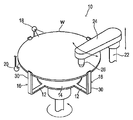
도 4는 도 1에 도시하는 펜슬 스크럽 세정 장치에 적용한, 본 발명의 실시 형태의 기판 처리 장치의 개요를 도시하는 평면도.
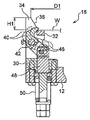
도 5는 도 4의 펜슬 스크럽 세정기(기판 처리 장치)의 기판 척 기구를 도시하는 단면도.
도 6의 (a)는 도 5에 도시하는 기판 척 기구의 주요부를, 도 2에 도시하는 기판 척 기구의 내주면을 가이드면으로 한 가이드부 및 도 3에 도시하는 기판 척 기구의 내주면을 가이드면으로 한 가이드부와 함께 도시하는 주요부 확대 단면도.
도 6의 (b)는 제1 가이드면(52a) 및 제2 가이드면(52b)으로 구성되는 가이드면(36b)을 도시하는 개략 단면도.
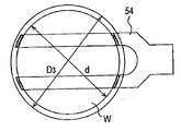
도 7은 로봇 핸드, 기판의 직경 d 및 가이드부의 제1 가이드면의 상단부를 원호 형상으로 연결하여 형성되는 개구(퍼올림구) 내경 D3의 관계를 나타내는 도면.
도 8은 본 발명의 다른 실시 형태의 기판 처리 장치의 개요를 도시하는 평면도.
도 9는 본 발명의 또 다른 실시 형태의 기판 처리 장치의 개요를 도시하는 평면도.
12 : 아암
14a : 기판 스테이지
16b : 기판 척 기구
24 : 요동 아암
26 : 펜슬형 세정구
30 : 척 본체
32, 56 : 기판 적재부
34b : 가이드부
36b : 가이드면
40 : 척 갈고리
48 : 개방 핀
50 : 코일 스프링
52a : 제1 가이드면
52b : 제2 가이드면
Claims (6)
- 기판의 주연부를 파지하여 기판을 회전시켜 처리하는 기판 처리 장치에 있어서,
방사상으로 연장되는 복수의 아암을 갖는 회전 가능한 기판 스테이지와,
상기 아암의 선단에 각각 고정되어 기판의 주연부를 파지하는 기판 척 기구를 구비하고,
상기 기판 척 기구는,
기판의 주연부를 적재하는 기판 적재부와 상기 기판 적재부에 기판을 적재할 때에 기판의 외주 단부면을 가이드하여 상기 기판의 위치 결정을 행하는 가이드면을 갖는 척 본체와,
상기 척 본체에 회전 가능하게 지지되어, 내측으로 폐쇄하는 방향으로 회전하고, 기판의 주연부를 상기 기판 적재부와의 사이에서 끼움 지지하는 척 갈고리를 갖고,
상기 가이드면은 상기 기판 적재부에 기판을 적재 보유 지지할 때에 자중에 의해 하강하는 기판의 외주 단부면을 가이드하는 제1 가이드면과, 척 갈고리를 내측으로 폐쇄하는 방향으로 회전시켜 기판 주연부를 상기 기판 적재부와의 사이에서 끼움 지지할 때에 상기 척 갈고리에 접촉하면서 이동하는 기판의 외주 단부면을 가이드하는 제2 가이드면을 갖는 것을 특징으로 하는, 기판 처리 장치. - 제1항에 있어서, 상기 제1 가이드면의 상단부를 원호 형상으로 연결하여 형성되는 개구 내경은, 처리되는 기판의 외경에, 기판을 로봇 핸드로 보유 지지하여 반송하는 로봇의 위치 결정 오차의 최대값, 로봇 핸드 내에서의 기판의 어긋남 범위의 최대값 및 작업자의 티칭 오차의 최대값으로 이루어지는 3개의 최대값에 기초하여 계산한 값을 더하고, 또한 허용값을 더한 값이 되도록 설정되어 있는 것을 특징으로 하는, 기판 처리 장치.
- 제1항에 있어서, 상기 가이드부의 상기 기판 적재부 상면으로부터의 높이는 2.0㎜ 내지 5.0㎜인 것을 특징으로 하는, 기판 처리 장치.
- 제1항에 있어서, 상기 아암의 수를 8 이상으로 한 것을 특징으로 하는, 기판 처리 장치.
- 제1항에 있어서, 상기 기판 적재부를 링 형상으로 연속시킨 것을 특징으로 하는, 기판 처리 장치.
- 제5항에 있어서, 상기 링 형상으로 연속한 기판 적재부의 일부에, 로봇 핸드를 통과시키는 절결부를 형성한 것을 특징으로 하는, 기판 처리 장치.
Applications Claiming Priority (2)
| Application Number | Priority Date | Filing Date | Title |
|---|---|---|---|
| JP2012099340A JP6018404B2 (ja) | 2012-04-25 | 2012-04-25 | 基板処理装置 |
| JPJP-P-2012-099340 | 2012-04-25 |
Publications (2)
| Publication Number | Publication Date |
|---|---|
| KR20130120410A true KR20130120410A (ko) | 2013-11-04 |
| KR102094281B1 KR102094281B1 (ko) | 2020-03-30 |
Family
ID=49669289
Family Applications (1)
| Application Number | Title | Priority Date | Filing Date |
|---|---|---|---|
| KR1020130045495A Active KR102094281B1 (ko) | 2012-04-25 | 2013-04-24 | 기판 처리 장치 |
Country Status (4)
| Country | Link |
|---|---|
| US (1) | US9472441B2 (ko) |
| JP (1) | JP6018404B2 (ko) |
| KR (1) | KR102094281B1 (ko) |
| TW (1) | TWI596687B (ko) |
Cited By (2)
| Publication number | Priority date | Publication date | Assignee | Title |
|---|---|---|---|---|
| KR20160061263A (ko) * | 2014-11-21 | 2016-05-31 | 도쿄엘렉트론가부시키가이샤 | 기판 처리 시스템 |
| KR20200027687A (ko) * | 2018-09-05 | 2020-03-13 | 주식회사 케이씨텍 | 기판 처리 장치 |
Families Citing this family (15)
| Publication number | Priority date | Publication date | Assignee | Title |
|---|---|---|---|---|
| JP5712782B2 (ja) * | 2011-05-13 | 2015-05-07 | 株式会社Sumco | エピタキシャルウェーハ成長装置用サセプタサポートシャフトおよびエピタキシャル成長装置 |
| JP6181438B2 (ja) | 2013-06-24 | 2017-08-16 | 株式会社荏原製作所 | 基板保持装置および基板洗浄装置 |
| JP6331189B2 (ja) * | 2014-03-07 | 2018-05-30 | 株式会社Screenホールディングス | 基板処理装置 |
| JP6335103B2 (ja) * | 2014-11-14 | 2018-05-30 | 株式会社荏原製作所 | 基板保持装置 |
| US10276425B2 (en) * | 2014-11-21 | 2019-04-30 | Tokyo Electron Limited | Substrate processing system |
| JP6456712B2 (ja) | 2015-02-16 | 2019-01-23 | 東京エレクトロン株式会社 | 基板保持機構及びこれを用いた基板処理装置 |
| US9618857B2 (en) * | 2015-02-28 | 2017-04-11 | Kla-Tencor Corporation | End effectors and reticle handling at a high throughput |
| JP6946151B2 (ja) * | 2017-11-13 | 2021-10-06 | 株式会社荏原製作所 | 基板保持装置および基板保持装置を備える基板処理装置 |
| EP3918421B1 (en) * | 2019-12-26 | 2024-05-15 | Nanjing ZongAn Semiconductor Equipment Ltd | Tool architecture for wafer geometry measurement in semiconductor industry |
| US20230062723A1 (en) * | 2021-08-31 | 2023-03-02 | Illinois Tool Works Inc. | Systems and methods for mounting a grinder/polisher sample holder |
| WO2023037424A1 (ja) * | 2021-09-08 | 2023-03-16 | 株式会社日立ハイテク | ウェハ検査装置 |
| US20230390898A1 (en) * | 2022-06-07 | 2023-12-07 | Ebara Corporation | Substrate clamping apparatus |
| CN115472553B (zh) * | 2022-11-11 | 2023-05-02 | 苏州智程半导体科技股份有限公司 | 一种半导体晶圆刻蚀或清洗的夹定装置 |
| US12525468B2 (en) | 2022-12-30 | 2026-01-13 | Applied Materials, Inc. | Integrated clean and dry module for cleaning a substrate |
| CN121192043A (zh) * | 2024-06-21 | 2025-12-23 | 盛美半导体设备(上海)股份有限公司 | 用于方形基板的卡盘 |
Citations (7)
| Publication number | Priority date | Publication date | Assignee | Title |
|---|---|---|---|---|
| JPS512322A (en) | 1974-05-20 | 1976-01-09 | Matsushita Electric Industrial Co Ltd | Seishigahosojushinsochi |
| JPH08255776A (ja) | 1995-01-19 | 1996-10-01 | Tokyo Electron Ltd | 洗浄装置および洗浄方法 |
| JPH1059540A (ja) | 1996-05-13 | 1998-03-03 | Ebara Corp | 基板把持装置 |
| JP2002319613A (ja) * | 2001-04-23 | 2002-10-31 | Topcon Corp | ウェーハ保持装置 |
| JP2003303871A (ja) | 2002-04-11 | 2003-10-24 | Nisso Engineering Co Ltd | ウエハ保持装置及び保持方法 |
| JP2004273847A (ja) * | 2003-03-10 | 2004-09-30 | Tokyo Electron Ltd | 基板搬送装置 |
| JP2004356517A (ja) | 2003-05-30 | 2004-12-16 | Ebara Corp | 基板洗浄装置及び基板洗浄方法 |
Family Cites Families (15)
| Publication number | Priority date | Publication date | Assignee | Title |
|---|---|---|---|---|
| US5775000A (en) * | 1996-05-13 | 1998-07-07 | Ebara Corporation | Substrate gripper device for spin drying |
| JP3512322B2 (ja) | 1997-12-15 | 2004-03-29 | 大日本スクリーン製造株式会社 | 枚葉式基板処理装置 |
| US6167893B1 (en) * | 1999-02-09 | 2001-01-02 | Novellus Systems, Inc. | Dynamic chuck for semiconductor wafer or other substrate |
| KR100445259B1 (ko) * | 2001-11-27 | 2004-08-21 | 삼성전자주식회사 | 세정방법 및 이를 수행하기 위한 세정 장치 |
| JP4275420B2 (ja) * | 2003-01-28 | 2009-06-10 | 大日本スクリーン製造株式会社 | 基板処理装置および基板処理方法 |
| JP4305749B2 (ja) * | 2003-10-02 | 2009-07-29 | 株式会社安川電機 | 基板保持装置 |
| JP2007523463A (ja) * | 2004-02-24 | 2007-08-16 | 株式会社荏原製作所 | 基板処理装置及び方法 |
| KR100672937B1 (ko) * | 2004-07-19 | 2007-01-24 | 삼성전자주식회사 | 반도체 기판 처리 장치 |
| JP4814731B2 (ja) * | 2006-08-30 | 2011-11-16 | 株式会社日立ハイテクノロジーズ | 基板保持装置、検査または処理の装置、基板保持方法、検査または処理の方法および検査装置 |
| JP4920387B2 (ja) * | 2006-12-01 | 2012-04-18 | 信越半導体株式会社 | 基板収納容器 |
| JP4825771B2 (ja) * | 2007-10-22 | 2011-11-30 | 信越ポリマー株式会社 | ウェーハ収納容器およびウェーハのハンドリング方法 |
| US8118940B2 (en) * | 2008-02-07 | 2012-02-21 | Asm Japan K.K. | Clamping mechanism for semiconductor device |
| JP2010021257A (ja) * | 2008-07-09 | 2010-01-28 | Hitachi High-Tech Control Systems Corp | ウェーハアライメント装置及びそれを用いたウェーハ搬送装置 |
| JP2010258170A (ja) * | 2009-04-23 | 2010-11-11 | Tokyo Electron Ltd | 基板保持部材、基板搬送アーム及び基板搬送装置 |
| JP6053528B2 (ja) * | 2013-01-11 | 2016-12-27 | 株式会社荏原製作所 | 基板把持装置 |
-
2012
- 2012-04-25 JP JP2012099340A patent/JP6018404B2/ja active Active
-
2013
- 2013-04-23 TW TW102114334A patent/TWI596687B/zh active
- 2013-04-24 US US13/869,849 patent/US9472441B2/en active Active
- 2013-04-24 KR KR1020130045495A patent/KR102094281B1/ko active Active
Patent Citations (7)
| Publication number | Priority date | Publication date | Assignee | Title |
|---|---|---|---|---|
| JPS512322A (en) | 1974-05-20 | 1976-01-09 | Matsushita Electric Industrial Co Ltd | Seishigahosojushinsochi |
| JPH08255776A (ja) | 1995-01-19 | 1996-10-01 | Tokyo Electron Ltd | 洗浄装置および洗浄方法 |
| JPH1059540A (ja) | 1996-05-13 | 1998-03-03 | Ebara Corp | 基板把持装置 |
| JP2002319613A (ja) * | 2001-04-23 | 2002-10-31 | Topcon Corp | ウェーハ保持装置 |
| JP2003303871A (ja) | 2002-04-11 | 2003-10-24 | Nisso Engineering Co Ltd | ウエハ保持装置及び保持方法 |
| JP2004273847A (ja) * | 2003-03-10 | 2004-09-30 | Tokyo Electron Ltd | 基板搬送装置 |
| JP2004356517A (ja) | 2003-05-30 | 2004-12-16 | Ebara Corp | 基板洗浄装置及び基板洗浄方法 |
Cited By (2)
| Publication number | Priority date | Publication date | Assignee | Title |
|---|---|---|---|---|
| KR20160061263A (ko) * | 2014-11-21 | 2016-05-31 | 도쿄엘렉트론가부시키가이샤 | 기판 처리 시스템 |
| KR20200027687A (ko) * | 2018-09-05 | 2020-03-13 | 주식회사 케이씨텍 | 기판 처리 장치 |
Also Published As
| Publication number | Publication date |
|---|---|
| JP6018404B2 (ja) | 2016-11-02 |
| TWI596687B (zh) | 2017-08-21 |
| US9472441B2 (en) | 2016-10-18 |
| KR102094281B1 (ko) | 2020-03-30 |
| JP2013229409A (ja) | 2013-11-07 |
| TW201351541A (zh) | 2013-12-16 |
| US20130320636A1 (en) | 2013-12-05 |
Similar Documents
| Publication | Publication Date | Title |
|---|---|---|
| KR20130120410A (ko) | 기판 처리 장치 | |
| US9165799B2 (en) | Substrate processing method and substrate processing unit | |
| KR102465094B1 (ko) | 기판 처리 장치, 기판 처리 방법 및 기억 매체 | |
| CN103706499B (zh) | 基板清洗装置及研磨装置 | |
| CN114472332A (zh) | 一种浸泡式去胶清洗、干燥一体机 | |
| CN107221491A (zh) | 基板清洗装置 | |
| KR102402297B1 (ko) | 기판 처리 장치 및 기판 처리 방법 | |
| US10643872B2 (en) | Liquid processing apparatus, liquid processing method, and storage medium | |
| JP2017188665A (ja) | 基板処理装置及び基板処理方法 | |
| US11410857B2 (en) | Wafer holding pins and methods of using the same | |
| CN205670538U (zh) | 一种集成式晶圆卡盘 | |
| JP7057673B2 (ja) | 加工装置 | |
| KR20090029407A (ko) | 지지부재 및 이를 구비하는 기판 처리 장치 | |
| CN105097438A (zh) | 一种晶片背面清洗装置 | |
| JPH10177999A (ja) | 基板搬送用ハンド及びポリッシング装置 | |
| JP6595040B2 (ja) | 基板処理装置及び基板搬送方法 | |
| JP6952579B2 (ja) | 基板処理装置および基板処理方法 | |
| US11948827B2 (en) | Substrate support mechanism, substrate cleaning device and substrate processing method | |
| JP5689367B2 (ja) | 基板搬送方法および基板搬送機 | |
| JP2019192853A (ja) | 洗浄装置 | |
| JP7336967B2 (ja) | 基板処理装置、および基板処理方法 | |
| CN111799209B (zh) | 基板支承装置以及基板支承装置的控制方法 | |
| JP6144531B2 (ja) | 基板処理装置及び処理基板の製造方法 | |
| JP6122684B2 (ja) | 基板処理装置及び処理基板の製造方法 | |
| KR20070118205A (ko) | 웨이퍼 세정 장치의 척 구조 |
Legal Events
| Date | Code | Title | Description |
|---|---|---|---|
| PA0109 | Patent application |
St.27 status event code: A-0-1-A10-A12-nap-PA0109 |
|
| P11-X000 | Amendment of application requested |
St.27 status event code: A-2-2-P10-P11-nap-X000 |
|
| PE0801 | Dismissal of amendment |
St.27 status event code: A-2-2-P10-P12-nap-PE0801 |
|
| PG1501 | Laying open of application |
St.27 status event code: A-1-1-Q10-Q12-nap-PG1501 |
|
| A201 | Request for examination | ||
| P11-X000 | Amendment of application requested |
St.27 status event code: A-2-2-P10-P11-nap-X000 |
|
| P13-X000 | Application amended |
St.27 status event code: A-2-2-P10-P13-nap-X000 |
|
| PA0201 | Request for examination |
St.27 status event code: A-1-2-D10-D11-exm-PA0201 |
|
| R18-X000 | Changes to party contact information recorded |
St.27 status event code: A-3-3-R10-R18-oth-X000 |
|
| E902 | Notification of reason for refusal | ||
| PE0902 | Notice of grounds for rejection |
St.27 status event code: A-1-2-D10-D21-exm-PE0902 |
|
| R18-X000 | Changes to party contact information recorded |
St.27 status event code: A-3-3-R10-R18-oth-X000 |
|
| T11-X000 | Administrative time limit extension requested |
St.27 status event code: U-3-3-T10-T11-oth-X000 |
|
| P11-X000 | Amendment of application requested |
St.27 status event code: A-2-2-P10-P11-nap-X000 |
|
| P13-X000 | Application amended |
St.27 status event code: A-2-2-P10-P13-nap-X000 |
|
| E701 | Decision to grant or registration of patent right | ||
| PE0701 | Decision of registration |
St.27 status event code: A-1-2-D10-D22-exm-PE0701 |
|
| GRNT | Written decision to grant | ||
| PR0701 | Registration of establishment |
St.27 status event code: A-2-4-F10-F11-exm-PR0701 |
|
| PR1002 | Payment of registration fee |
St.27 status event code: A-2-2-U10-U11-oth-PR1002 Fee payment year number: 1 |
|
| PG1601 | Publication of registration |
St.27 status event code: A-4-4-Q10-Q13-nap-PG1601 |
|
| PR1001 | Payment of annual fee |
St.27 status event code: A-4-4-U10-U11-oth-PR1001 Fee payment year number: 4 |
|
| PR1001 | Payment of annual fee |
St.27 status event code: A-4-4-U10-U11-oth-PR1001 Fee payment year number: 5 |
|
| PR1001 | Payment of annual fee |
St.27 status event code: A-4-4-U10-U11-oth-PR1001 Fee payment year number: 6 |
|
| P22-X000 | Classification modified |
St.27 status event code: A-4-4-P10-P22-nap-X000 |