KR20140051692A - 전자부품들이 구비된 기판구조 및 전자부품들이 구비된 기판구조의 제조방법 - Google Patents
전자부품들이 구비된 기판구조 및 전자부품들이 구비된 기판구조의 제조방법 Download PDFInfo
- Publication number
- KR20140051692A KR20140051692A KR1020120118028A KR20120118028A KR20140051692A KR 20140051692 A KR20140051692 A KR 20140051692A KR 1020120118028 A KR1020120118028 A KR 1020120118028A KR 20120118028 A KR20120118028 A KR 20120118028A KR 20140051692 A KR20140051692 A KR 20140051692A
- Authority
- KR
- South Korea
- Prior art keywords
- terminal
- electronic component
- circuit pattern
- substrate
- electronic components
- Prior art date
- Legal status (The legal status is an assumption and is not a legal conclusion. Google has not performed a legal analysis and makes no representation as to the accuracy of the status listed.)
- Granted
Links
Images


Classifications
-
- H—ELECTRICITY
- H05—ELECTRIC TECHNIQUES NOT OTHERWISE PROVIDED FOR
- H05K—PRINTED CIRCUITS; CASINGS OR CONSTRUCTIONAL DETAILS OF ELECTRIC APPARATUS; MANUFACTURE OF ASSEMBLAGES OF ELECTRICAL COMPONENTS
- H05K1/00—Printed circuits
- H05K1/18—Printed circuits structurally associated with non-printed electric components
- H05K1/182—Printed circuits structurally associated with non-printed electric components associated with components mounted in printed circuit boards [PCB], e.g. insert-mounted components [IMC]
- H05K1/185—Printed circuits structurally associated with non-printed electric components associated with components mounted in printed circuit boards [PCB], e.g. insert-mounted components [IMC] associated with components encapsulated in the insulating substrate of the PCBs; associated with components incorporated in internal layers of multilayer circuit boards
-
- H—ELECTRICITY
- H05—ELECTRIC TECHNIQUES NOT OTHERWISE PROVIDED FOR
- H05K—PRINTED CIRCUITS; CASINGS OR CONSTRUCTIONAL DETAILS OF ELECTRIC APPARATUS; MANUFACTURE OF ASSEMBLAGES OF ELECTRICAL COMPONENTS
- H05K1/00—Printed circuits
- H05K1/18—Printed circuits structurally associated with non-printed electric components
-
- H—ELECTRICITY
- H05—ELECTRIC TECHNIQUES NOT OTHERWISE PROVIDED FOR
- H05K—PRINTED CIRCUITS; CASINGS OR CONSTRUCTIONAL DETAILS OF ELECTRIC APPARATUS; MANUFACTURE OF ASSEMBLAGES OF ELECTRICAL COMPONENTS
- H05K3/00—Apparatus or processes for manufacturing printed circuits
- H05K3/46—Manufacturing multilayer circuits
- H05K3/4697—Manufacturing multilayer circuits having cavities, e.g. for mounting components
-
- H—ELECTRICITY
- H05—ELECTRIC TECHNIQUES NOT OTHERWISE PROVIDED FOR
- H05K—PRINTED CIRCUITS; CASINGS OR CONSTRUCTIONAL DETAILS OF ELECTRIC APPARATUS; MANUFACTURE OF ASSEMBLAGES OF ELECTRICAL COMPONENTS
- H05K3/00—Apparatus or processes for manufacturing printed circuits
- H05K3/46—Manufacturing multilayer circuits
-
- H—ELECTRICITY
- H05—ELECTRIC TECHNIQUES NOT OTHERWISE PROVIDED FOR
- H05K—PRINTED CIRCUITS; CASINGS OR CONSTRUCTIONAL DETAILS OF ELECTRIC APPARATUS; MANUFACTURE OF ASSEMBLAGES OF ELECTRICAL COMPONENTS
- H05K1/00—Printed circuits
- H05K1/02—Details
- H05K1/0213—Electrical arrangements not otherwise provided for
- H05K1/0216—Reduction of cross-talk, noise or electromagnetic interference
- H05K1/023—Reduction of cross-talk, noise or electromagnetic interference using auxiliary mounted passive components or auxiliary substances
- H05K1/0231—Capacitors or dielectric substances
-
- H—ELECTRICITY
- H05—ELECTRIC TECHNIQUES NOT OTHERWISE PROVIDED FOR
- H05K—PRINTED CIRCUITS; CASINGS OR CONSTRUCTIONAL DETAILS OF ELECTRIC APPARATUS; MANUFACTURE OF ASSEMBLAGES OF ELECTRICAL COMPONENTS
- H05K1/00—Printed circuits
- H05K1/18—Printed circuits structurally associated with non-printed electric components
- H05K1/181—Printed circuits structurally associated with non-printed electric components associated with surface mounted components
-
- H—ELECTRICITY
- H05—ELECTRIC TECHNIQUES NOT OTHERWISE PROVIDED FOR
- H05K—PRINTED CIRCUITS; CASINGS OR CONSTRUCTIONAL DETAILS OF ELECTRIC APPARATUS; MANUFACTURE OF ASSEMBLAGES OF ELECTRICAL COMPONENTS
- H05K2201/00—Indexing scheme relating to printed circuits covered by H05K1/00
- H05K2201/10—Details of components or other objects attached to or integrated in a printed circuit board
- H05K2201/10431—Details of mounted components
- H05K2201/10507—Involving several components
- H05K2201/1053—Mounted components directly electrically connected to each other, i.e. not via the PCB
-
- H—ELECTRICITY
- H05—ELECTRIC TECHNIQUES NOT OTHERWISE PROVIDED FOR
- H05K—PRINTED CIRCUITS; CASINGS OR CONSTRUCTIONAL DETAILS OF ELECTRIC APPARATUS; MANUFACTURE OF ASSEMBLAGES OF ELECTRICAL COMPONENTS
- H05K2201/00—Indexing scheme relating to printed circuits covered by H05K1/00
- H05K2201/10—Details of components or other objects attached to or integrated in a printed circuit board
- H05K2201/10613—Details of electrical connections of non-printed components, e.g. special leads
- H05K2201/10621—Components characterised by their electrical contacts
- H05K2201/10636—Leadless chip, e.g. chip capacitor or resistor
-
- H—ELECTRICITY
- H05—ELECTRIC TECHNIQUES NOT OTHERWISE PROVIDED FOR
- H05K—PRINTED CIRCUITS; CASINGS OR CONSTRUCTIONAL DETAILS OF ELECTRIC APPARATUS; MANUFACTURE OF ASSEMBLAGES OF ELECTRICAL COMPONENTS
- H05K2201/00—Indexing scheme relating to printed circuits covered by H05K1/00
- H05K2201/10—Details of components or other objects attached to or integrated in a printed circuit board
- H05K2201/10613—Details of electrical connections of non-printed components, e.g. special leads
- H05K2201/10621—Components characterised by their electrical contacts
- H05K2201/10674—Flip chip
-
- H—ELECTRICITY
- H05—ELECTRIC TECHNIQUES NOT OTHERWISE PROVIDED FOR
- H05K—PRINTED CIRCUITS; CASINGS OR CONSTRUCTIONAL DETAILS OF ELECTRIC APPARATUS; MANUFACTURE OF ASSEMBLAGES OF ELECTRICAL COMPONENTS
- H05K2203/00—Indexing scheme relating to apparatus or processes for manufacturing printed circuits covered by H05K3/00
- H05K2203/14—Related to the order of processing steps
- H05K2203/1461—Applying or finishing the circuit pattern after another process, e.g. after filling of vias with conductive paste, after making printed resistors
- H05K2203/1469—Circuit made after mounting or encapsulation of the components
-
- H—ELECTRICITY
- H05—ELECTRIC TECHNIQUES NOT OTHERWISE PROVIDED FOR
- H05K—PRINTED CIRCUITS; CASINGS OR CONSTRUCTIONAL DETAILS OF ELECTRIC APPARATUS; MANUFACTURE OF ASSEMBLAGES OF ELECTRICAL COMPONENTS
- H05K3/00—Apparatus or processes for manufacturing printed circuits
- H05K3/30—Assembling printed circuits with electric components, e.g. with resistors
- H05K3/32—Assembling printed circuits with electric components, e.g. with resistors electrically connecting electric components or wires to printed circuits
- H05K3/34—Assembling printed circuits with electric components, e.g. with resistors electrically connecting electric components or wires to printed circuits by soldering
- H05K3/341—Surface mounted components
- H05K3/3431—Leadless components
- H05K3/3436—Leadless components having an array of bottom contacts, e.g. pad grid array or ball grid array components
-
- H—ELECTRICITY
- H10—SEMICONDUCTOR DEVICES; ELECTRIC SOLID-STATE DEVICES NOT OTHERWISE PROVIDED FOR
- H10W—GENERIC PACKAGES, INTERCONNECTIONS, CONNECTORS OR OTHER CONSTRUCTIONAL DETAILS OF DEVICES COVERED BY CLASS H10
- H10W74/00—Encapsulations, e.g. protective coatings
- H10W74/10—Encapsulations, e.g. protective coatings characterised by their shape or disposition
- H10W74/131—Encapsulations, e.g. protective coatings characterised by their shape or disposition the semiconductor body being only partially enclosed
- H10W74/142—Encapsulations, e.g. protective coatings characterised by their shape or disposition the semiconductor body being only partially enclosed the encapsulations exposing the passive side of the semiconductor body
-
- H—ELECTRICITY
- H10—SEMICONDUCTOR DEVICES; ELECTRIC SOLID-STATE DEVICES NOT OTHERWISE PROVIDED FOR
- H10W—GENERIC PACKAGES, INTERCONNECTIONS, CONNECTORS OR OTHER CONSTRUCTIONAL DETAILS OF DEVICES COVERED BY CLASS H10
- H10W90/00—Package configurations
- H10W90/701—Package configurations characterised by the relative positions of pads or connectors relative to package parts
- H10W90/721—Package configurations characterised by the relative positions of pads or connectors relative to package parts of bump connectors
- H10W90/724—Package configurations characterised by the relative positions of pads or connectors relative to package parts of bump connectors between a chip and a stacked insulating package substrate, interposer or RDL
-
- H—ELECTRICITY
- H10—SEMICONDUCTOR DEVICES; ELECTRIC SOLID-STATE DEVICES NOT OTHERWISE PROVIDED FOR
- H10W—GENERIC PACKAGES, INTERCONNECTIONS, CONNECTORS OR OTHER CONSTRUCTIONAL DETAILS OF DEVICES COVERED BY CLASS H10
- H10W90/00—Package configurations
- H10W90/701—Package configurations characterised by the relative positions of pads or connectors relative to package parts
- H10W90/721—Package configurations characterised by the relative positions of pads or connectors relative to package parts of bump connectors
- H10W90/728—Package configurations characterised by the relative positions of pads or connectors relative to package parts of bump connectors between a chip and a stacked discrete passive device, e.g. resistors, capacitors or inductors
-
- Y—GENERAL TAGGING OF NEW TECHNOLOGICAL DEVELOPMENTS; GENERAL TAGGING OF CROSS-SECTIONAL TECHNOLOGIES SPANNING OVER SEVERAL SECTIONS OF THE IPC; TECHNICAL SUBJECTS COVERED BY FORMER USPC CROSS-REFERENCE ART COLLECTIONS [XRACs] AND DIGESTS
- Y02—TECHNOLOGIES OR APPLICATIONS FOR MITIGATION OR ADAPTATION AGAINST CLIMATE CHANGE
- Y02P—CLIMATE CHANGE MITIGATION TECHNOLOGIES IN THE PRODUCTION OR PROCESSING OF GOODS
- Y02P70/00—Climate change mitigation technologies in the production process for final industrial or consumer products
- Y02P70/50—Manufacturing or production processes characterised by the final manufactured product
-
- Y—GENERAL TAGGING OF NEW TECHNOLOGICAL DEVELOPMENTS; GENERAL TAGGING OF CROSS-SECTIONAL TECHNOLOGIES SPANNING OVER SEVERAL SECTIONS OF THE IPC; TECHNICAL SUBJECTS COVERED BY FORMER USPC CROSS-REFERENCE ART COLLECTIONS [XRACs] AND DIGESTS
- Y10—TECHNICAL SUBJECTS COVERED BY FORMER USPC
- Y10T—TECHNICAL SUBJECTS COVERED BY FORMER US CLASSIFICATION
- Y10T29/00—Metal working
- Y10T29/49—Method of mechanical manufacture
- Y10T29/49002—Electrical device making
- Y10T29/49117—Conductor or circuit manufacturing
- Y10T29/49124—On flat or curved insulated base, e.g., printed circuit, etc.
- Y10T29/4913—Assembling to base an electrical component, e.g., capacitor, etc.
- Y10T29/49139—Assembling to base an electrical component, e.g., capacitor, etc. by inserting component lead or terminal into base aperture
- Y10T29/4914—Assembling to base an electrical component, e.g., capacitor, etc. by inserting component lead or terminal into base aperture with deforming of lead or terminal
- Y10T29/49142—Assembling to base an electrical component, e.g., capacitor, etc. by inserting component lead or terminal into base aperture with deforming of lead or terminal including metal fusion
Landscapes
- Engineering & Computer Science (AREA)
- Microelectronics & Electronic Packaging (AREA)
- Manufacturing & Machinery (AREA)
- Structures For Mounting Electric Components On Printed Circuit Boards (AREA)
- Production Of Multi-Layered Print Wiring Board (AREA)
Abstract
Description
도 2a 내지 도 2f는 본 발명의 일실시예에 따른 전자부품들이 구비된 기판구조의 제조방법을 개략적으로 예시한 공정단면도이다.
도 3은 본 발명의 다른 실시예에 따른 전자부품들이 구비된 기판구조를 개략적으로 예시한 단면도이다.
도 4a 내지 도 4g는 본 발명의 다른 실시예에 따른 전자부품들이 구비된 기판구조의 제조방법을 개략적으로 예시한 공정단면도이다.
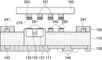
110 : 기판
111 : 캐비티
120 : 제1 전자부품
121 : 제1 단자
130 : 충진재
141, 241 : 제1 회로패턴
142, 242 : 제2 회로패턴
143 : 제3 회로패턴
144 : 제4 회로패턴
145 : 도금단자
150 : 절연부
160 : 제2 전자부품
161 : 제2 단자
170, 270 : 솔더
180 : 몰딩부
240S : 씨드층
291 : 제1 표면처리층
292 : 제2 표면처리층
293 : 제3 표면처리층
DF : 디테치 필름
Claims (22)
- 일면 및 상기 일면에 대향되는 타면이 구비되며, 상기 일면과 타면 사이가 관통되어 형성되는 캐비티가 구비된 기판;
상기 기판의 일면에 구비되는 제1 회로패턴 및 제2 회로패턴;
상기 캐비티 내부에 삽입되고, 표면에 제1 단자가 형성된 제1 전자부품;
상기 캐비티와 상기 제1 전자부품 사이의 공간을 채우는 충진재;
상기 제1 전자부품의 제1 단자에 형성되는 도금단자; 및
상기 기판의 일면 상에 실장되며, 상기 도금단자에 전기적으로 연결되는 제2 단자를 구비하는 제2 전자부품;
을 포함하는
전자부품들이 구비된 기판구조.
- 청구항 1에 있어서,
상기 도금단자와 상기 제2 단자는 솔더를 매개로 직접 접촉되는 것인
전자부품들이 구비된 기판구조.
- 청구항 1에 있어서,
상기 도금단자와 상기 제2 회로패턴의 높이가 동일하며,
상기 제2 단자는 솔더를 매개로 상기 도금단자 및 상기 제2 회로패턴에 직접 접촉되는 것인
전자부품들이 구비된 기판구조.
- 청구항 1에 있어서,
상기 제1 회로패턴을 덮는 절연부를 더 포함하는
전자부품들이 구비된 기판구조.
- 청구항 1에 있어서,
상기 제2 전자부품과 상기 기판 사이의 영역에 충진되는 몰딩부를 더 포함하는
전자부품들이 구비된 기판구조.
- 청구항 1에 있어서,
상기 기판의 타면에 구비되는 제3 회로패턴 및 제4 회로패턴 중 적어도 하나를 더 포함하는
전자부품들이 구비된 기판구조.
- 청구항 1에 있어서,
상기 충진재는 플러그 잉크인
전자부품들이 구비된 기판구조.
- 일면 및 상기 일면에 대향되는 타면이 구비되며, 상기 일면과 타면 사이가 관통되어 형성되는 캐비티가 구비된 기판을 제공하는 단계;
상기 기판의 일면에 디테치 필름을 부착하는 단계;
표면에 제1 단자가 구비된 제1 전자부품을 상기 캐비티 내부에 삽입하여 상기 디테치 필름에 상기 제1 전자부품을 부착한 후, 상기 캐비티와 상기 제1 전자부품 사이의 공간에 충진재를 충진하여 상기 제1 전자부품을 고정하는 단계;
상기 제1 전자부품이 고정된 후, 상기 디테치 필름을 제거하는 단계;
상기 디테치 필름이 제거된 상기 기판의 일면에 제1 회로패턴 및 제2 회로패턴을 형성하는 단계;
상기 디테치 필름이 제거된 상기 제1 단자의 표면에 도금단자를 형성하는 단계; 및
적어도 하나의 제2 단자가 적어도 한 면에 구비된 제2 전자부품의 상기 제2 단자와 상기 도금단자가 전기적으로 연결되도록 상기 제2 전자부품을 실장하는 단계;
를 포함하는
전자부품들이 구비된 기판구조의 제조방법.
- 청구항 8에 있어서,
상기 제2 전자부품을 실장하는 단계는,
상기 도금단자와 상기 제2 단자가 솔더를 매개로 직접 접촉되도록 수행되는
전자부품들이 구비된 기판구조의 제조방법.
- 청구항 8에 있어서,
상기 제1 회로패턴 및 제2 회로패턴을 형성하는 단계와, 상기 도금단자를 형성하는 단계는, 상기 도금단자와 상기 제2 회로패턴의 높이가 같아지도록 동일한 공정에서 수행되며,
상기 제2 전자부품을 실장하는 단계는,
상기 제2 단자는 솔더를 매개로 상기 도금단자 및 상기 제2 회로패턴에 직접 접촉되도록 수행되는
전자부품들이 구비된 기판구조의 제조방법.
- 청구항 8에 있어서,
상기 제2 전자부품과 상기 기판 사이의 영역에 절연수지를 충진하여 몰딩부를 형성하는 단계를 더 포함하는
전자부품들이 구비된 기판구조의 제조방법.
- 청구항 8에 있어서,
상기 충진재는 플러그 잉크인
전자부품들이 구비된 기판구조의 제조방법.
- 일면 및 상기 일면에 대향되는 타면이 구비되며, 상기 일면과 타면 사이가 관통되어 형성되는 캐비티가 구비된 기판;
상기 기판의 일면에 구비되는 제1 회로패턴 및 제2 회로패턴;
상기 캐비티 내부에 일부가 삽입되고 나머지 부분은 상기 캐비티 외부로 돌출되며, 표면에 제1 단자가 형성된 제1 전자부품;
상기 캐비티와 상기 제1 전자부품 사이의 공간을 채우는 충진재;
상기 제1 전자부품의 제1 단자의 상부면에 구비되는 제1 표면처리층; 및
상기 기판의 일면 상에 실장되며, 상기 제1 표면처리층에 전기적으로 연결되는 제2 단자를 구비하는 제2 전자부품;
을 포함하는
전자부품들이 구비된 기판구조.
- 청구항 13에 있어서,
상기 제1 전자부품의 일면은,
상기 제2 회로패턴의 상부면이 위치하는 수평면과 동일한 수평면에 위치되는 것인
전자부품들이 구비된 기판구조.
- 청구항 13에 있어서,
상기 제1 표면처리층과 상기 제2 단자는 솔더를 매개로 직접 접촉되는 것인
전자부품들이 구비된 기판구조.
- 청구항 13에 있어서,
상기 제2 회로패턴의 상부면에 구비되는 제2 표면처리층을 더 포함하며,
상기 제2 단자는 솔더를 매개로 상기 제1 표면처리층 및 상기 제2 회로패턴에 직접 접촉되는 것인
전자부품들이 구비된 기판구조.
- 청구항 13에 있어서,
상기 제2 단자의 하부면에 구비되는 제3 표면처리층을 더 포함하며,
상기 제3 표면처리층은 솔더를 매개로 상기 제1 표면처리층과 직접 접촉되는 것인
전자부품들이 구비된 기판구조.
- 일면 및 상기 일면에 대향되는 타면이 구비되며, 상기 일면에는 도전성 재질로 이루어지는 씨드층이 구비되고, 상기 씨드층의 상부면과 상기 타면 사이가 관통되어 형성되는 캐비티가 구비된 기판을 제공하는 단계;
상기 씨드층의 상부면에 디테치 필름을 부착하는 단계;
표면에 제1 단자가 구비된 제1 전자부품을 상기 캐비티 내부에 삽입하여 상기 디테치 필름에 상기 제1 전자부품을 부착한 후, 상기 캐비티와 상기 제1 전자부품 사이의 공간에 충진재를 충진하여 상기 제1 전자부품을 고정하는 단계;
상기 제1 전자부품이 고정된 후, 상기 디테치 필름을 제거하는 단계;
상기 디테치 필름이 제거된 상기 씨드층을 패터닝하여 제1 회로패턴 및 제2 회로패턴을 형성하는 단계;
상기 디테치 필름이 제거된 상기 제1 단자의 표면에 제1 표면처리층을 형성하는 단계; 및
적어도 하나의 제2 단자가 적어도 한 면에 구비된 제2 전자부품의 상기 제2 단자와 상기 제1 표면처리층이 전기적으로 연결되도록 상기 제2 전자부품을 실장하는 단계;
를 포함하는
전자부품들이 구비된 기판구조의 제조방법.
- 청구항 18에 있어서,
상기 제2 전자부품을 실장하는 단계는,
상기 제1 표면처리층과 상기 제2 단자가 솔더를 매개로 직접 접촉되도록 수행되는
전자부품들이 구비된 기판구조의 제조방법.
- 청구항 18에 있어서,
상기 제2 회로패턴의 상부면에 제2 표면처리층을 형성하는 단계를 더 포함하되, 상기 제1 표면처리층과 상기 제2 표면처리층의 상부면은 동일한 수평면 상에 존재하며,
상기 제2 전자부품을 실장하는 단계는,
상기 제1 표면처리층 및 상기 제2 표면처리층이 솔더를 매개로 상기 제2 단자와 적접 접촉되도록 수행되는
전자부품들이 구비된 기판구조의 제조방법.
- 청구항 18에 있어서,
상기 제2 단자의 하부면에 제3 표면처리층을 형성하는 단계를 더 포함하며,
상기 제2 전자부품을 실장하는 단계는,
상기 제3 표면처리층은 솔더를 매개로 상기 제1 표면처리층과 직접 접촉되도록 수행되는 것인
전자부품들이 구비된 기판구조의 제조방법.
- 청구항 18에 있어서,
상기 제1 표면처리층은 금-기반 SF 코팅층인
전자부품들이 구비된 기판구조의 제조방법.
Priority Applications (4)
| Application Number | Priority Date | Filing Date | Title |
|---|---|---|---|
| KR1020120118028A KR101420514B1 (ko) | 2012-10-23 | 2012-10-23 | 전자부품들이 구비된 기판구조 및 전자부품들이 구비된 기판구조의 제조방법 |
| TW102124537A TWI565381B (zh) | 2012-10-23 | 2013-07-09 | 具有電子元件之基板結構與製造具有電子元件之基板結構之方法 |
| US13/956,293 US9485878B2 (en) | 2012-10-23 | 2013-07-31 | Substrate structure having electronic components and method of manufacturing substrate structure having electronic components |
| JP2013161180A JP5934154B2 (ja) | 2012-10-23 | 2013-08-02 | 電子部品が実装された基板構造及びその製造方法 |
Applications Claiming Priority (1)
| Application Number | Priority Date | Filing Date | Title |
|---|---|---|---|
| KR1020120118028A KR101420514B1 (ko) | 2012-10-23 | 2012-10-23 | 전자부품들이 구비된 기판구조 및 전자부품들이 구비된 기판구조의 제조방법 |
Publications (2)
| Publication Number | Publication Date |
|---|---|
| KR20140051692A true KR20140051692A (ko) | 2014-05-02 |
| KR101420514B1 KR101420514B1 (ko) | 2014-07-17 |
Family
ID=50485140
Family Applications (1)
| Application Number | Title | Priority Date | Filing Date |
|---|---|---|---|
| KR1020120118028A Expired - Fee Related KR101420514B1 (ko) | 2012-10-23 | 2012-10-23 | 전자부품들이 구비된 기판구조 및 전자부품들이 구비된 기판구조의 제조방법 |
Country Status (4)
| Country | Link |
|---|---|
| US (1) | US9485878B2 (ko) |
| JP (1) | JP5934154B2 (ko) |
| KR (1) | KR101420514B1 (ko) |
| TW (1) | TWI565381B (ko) |
Cited By (1)
| Publication number | Priority date | Publication date | Assignee | Title |
|---|---|---|---|---|
| CN114342566A (zh) * | 2019-09-04 | 2022-04-12 | Tdk株式会社 | 电子部件安装结构 |
Families Citing this family (7)
| Publication number | Priority date | Publication date | Assignee | Title |
|---|---|---|---|---|
| KR101514518B1 (ko) * | 2013-05-24 | 2015-04-22 | 삼성전기주식회사 | 전자부품 내장 인쇄회로기판 및 그 제조방법 |
| KR102356810B1 (ko) * | 2015-01-22 | 2022-01-28 | 삼성전기주식회사 | 전자부품내장형 인쇄회로기판 및 그 제조방법 |
| JP2018026435A (ja) * | 2016-08-09 | 2018-02-15 | 株式会社村田製作所 | 部品内蔵基板 |
| FR3062546B1 (fr) * | 2017-02-01 | 2021-09-10 | Inst Vedecom | Structure de diffraction integree dans une carte de circuit imprime et procede de fabrication de celle-ci |
| CN113766731A (zh) * | 2020-06-02 | 2021-12-07 | 苏州旭创科技有限公司 | 一种电路板组件的组装方法 |
| KR20220155036A (ko) * | 2021-05-14 | 2022-11-22 | 삼성전자주식회사 | 반도체 패키지 |
| WO2024206156A1 (en) * | 2023-03-24 | 2024-10-03 | Samtec, Inc. | Connector and method of use without preattached solder ball |
Family Cites Families (25)
| Publication number | Priority date | Publication date | Assignee | Title |
|---|---|---|---|---|
| TW373308B (en) * | 1995-02-24 | 1999-11-01 | Agere Systems Inc | Thin packaging of multi-chip modules with enhanced thermal/power management |
| US5963429A (en) * | 1997-08-20 | 1999-10-05 | Sulzer Intermedics Inc. | Printed circuit substrate with cavities for encapsulating integrated circuits |
| JP3792445B2 (ja) * | 1999-03-30 | 2006-07-05 | 日本特殊陶業株式会社 | コンデンサ付属配線基板 |
| US6228682B1 (en) * | 1999-12-21 | 2001-05-08 | International Business Machines Corporation | Multi-cavity substrate structure for discrete devices |
| US6598780B2 (en) * | 1999-12-24 | 2003-07-29 | Denso Corporation | Method of connecting circuit boards |
| US6815829B2 (en) * | 2000-03-29 | 2004-11-09 | Rohm Co., Ltd. | Semiconductor device with compact package |
| JP2002289768A (ja) * | 2000-07-17 | 2002-10-04 | Rohm Co Ltd | 半導体装置およびその製法 |
| JP2002314031A (ja) * | 2001-04-13 | 2002-10-25 | Fujitsu Ltd | マルチチップモジュール |
| US6815126B2 (en) * | 2002-04-09 | 2004-11-09 | International Business Machines Corporation | Printed wiring board with conformally plated circuit traces |
| US6906415B2 (en) * | 2002-06-27 | 2005-06-14 | Micron Technology, Inc. | Semiconductor device assemblies and packages including multiple semiconductor devices and methods |
| JP4380130B2 (ja) | 2002-09-13 | 2009-12-09 | ソニー株式会社 | 半導体装置 |
| EP1627430B1 (en) * | 2003-05-28 | 2008-10-01 | Infineon Technologies AG | An integrated circuit package employing a flexible substrate |
| JP4198566B2 (ja) | 2003-09-29 | 2008-12-17 | 新光電気工業株式会社 | 電子部品内蔵基板の製造方法 |
| US7786591B2 (en) * | 2004-09-29 | 2010-08-31 | Broadcom Corporation | Die down ball grid array package |
| JP4581768B2 (ja) * | 2005-03-16 | 2010-11-17 | ソニー株式会社 | 半導体装置の製造方法 |
| KR100736635B1 (ko) * | 2006-02-09 | 2007-07-06 | 삼성전기주식회사 | 베어칩 내장형 인쇄회로기판 및 그 제조 방법 |
| KR100836651B1 (ko) * | 2007-01-16 | 2008-06-10 | 삼성전기주식회사 | 소자내장기판 및 그 제조방법 |
| KR100888579B1 (ko) * | 2007-02-27 | 2009-03-12 | 대덕전자 주식회사 | 고용량 반도체 칩 내장 인쇄회로기판 제조 방법 |
| JP2010161184A (ja) * | 2009-01-08 | 2010-07-22 | Hitachi Ltd | 半導体装置 |
| KR101084252B1 (ko) * | 2010-03-05 | 2011-11-17 | 삼성전기주식회사 | 전자소자 내장형 인쇄회로기판 및 그 제조방법 |
| KR101075645B1 (ko) * | 2010-08-18 | 2011-10-21 | 삼성전기주식회사 | 임베디드 회로기판의 제조 방법 |
| KR101181173B1 (ko) * | 2010-10-11 | 2012-09-18 | 엘지이노텍 주식회사 | 방열회로기판, 그의 제조 방법 및 그를 포함하는 발열소자 패키지 |
| KR101190920B1 (ko) * | 2010-10-18 | 2012-10-12 | 하나 마이크론(주) | 적층 반도체 패키지 및 그 제조 방법 |
| JP2012164952A (ja) | 2011-01-20 | 2012-08-30 | Ibiden Co Ltd | 電子部品内蔵配線板及びその製造方法 |
| JP2012186440A (ja) | 2011-02-18 | 2012-09-27 | Ibiden Co Ltd | インダクタ部品とその部品を内蔵しているプリント配線板及びインダクタ部品の製造方法 |
-
2012
- 2012-10-23 KR KR1020120118028A patent/KR101420514B1/ko not_active Expired - Fee Related
-
2013
- 2013-07-09 TW TW102124537A patent/TWI565381B/zh not_active IP Right Cessation
- 2013-07-31 US US13/956,293 patent/US9485878B2/en active Active
- 2013-08-02 JP JP2013161180A patent/JP5934154B2/ja not_active Expired - Fee Related
Cited By (2)
| Publication number | Priority date | Publication date | Assignee | Title |
|---|---|---|---|---|
| CN114342566A (zh) * | 2019-09-04 | 2022-04-12 | Tdk株式会社 | 电子部件安装结构 |
| CN114342566B (zh) * | 2019-09-04 | 2024-06-04 | Tdk株式会社 | 电子部件安装结构 |
Also Published As
| Publication number | Publication date |
|---|---|
| TWI565381B (zh) | 2017-01-01 |
| KR101420514B1 (ko) | 2014-07-17 |
| JP5934154B2 (ja) | 2016-06-15 |
| TW201417661A (zh) | 2014-05-01 |
| JP2014086721A (ja) | 2014-05-12 |
| US9485878B2 (en) | 2016-11-01 |
| US20140111958A1 (en) | 2014-04-24 |
Similar Documents
| Publication | Publication Date | Title |
|---|---|---|
| KR101420514B1 (ko) | 전자부품들이 구비된 기판구조 및 전자부품들이 구비된 기판구조의 제조방법 | |
| US8952262B2 (en) | Component-incorporated wiring substrate and method of manufacturing the same | |
| KR101420526B1 (ko) | 전자부품 내장기판 및 그 제조방법 | |
| KR101472638B1 (ko) | 수동소자 내장기판 | |
| JP5090749B2 (ja) | 半導体パッケージ及びその製造方法 | |
| CN105826306B (zh) | 芯片封装、封装基板及封装基板的制造方法 | |
| US20130258623A1 (en) | Package structure having embedded electronic element and fabrication method thereof | |
| US20150055309A1 (en) | Electronic component embedded substrate and method of manufacturing electronic component embedded substrate | |
| CN105990268B (zh) | 电子封装结构及其制法 | |
| KR101565690B1 (ko) | 회로기판, 회로기판 제조방법, 전자부품 패키지 및 전자부품 패키지 제조방법 | |
| US9101075B2 (en) | Substrate with built-in component | |
| JP6358664B2 (ja) | 回路アッセンブリ | |
| TW201429326A (zh) | 具有內埋元件的電路板、其製作方法及封裝結構 | |
| TWI646639B (zh) | 半導體封裝 | |
| KR20170124769A (ko) | 전자 소자 모듈 및 그 제조 방법 | |
| TWI485839B (zh) | 電子模組以及其製造方法 | |
| KR101167453B1 (ko) | 전자부품 내장형 인쇄회로기판 및 그 제조방법 | |
| TWI433278B (zh) | 無承載板之封裝件及其製法 | |
| TWI566330B (zh) | 電子封裝結構之製法 | |
| US9433108B2 (en) | Method of fabricating a circuit board structure having an embedded electronic element | |
| CN103887272B (zh) | 电子模块以及其制造方法 | |
| JP2010153491A5 (ja) | 電子装置及びその製造方法、並びに半導体装置 | |
| TW201603213A (zh) | 半導體封裝件及其製法 | |
| KR20110080491A (ko) | 반도체 칩 패키지 제조방법 | |
| TW201601224A (zh) | 封裝基板結構及其製法 |
Legal Events
| Date | Code | Title | Description |
|---|---|---|---|
| A201 | Request for examination | ||
| PA0109 | Patent application |
St.27 status event code: A-0-1-A10-A12-nap-PA0109 |
|
| PA0201 | Request for examination |
St.27 status event code: A-1-2-D10-D11-exm-PA0201 |
|
| D13-X000 | Search requested |
St.27 status event code: A-1-2-D10-D13-srh-X000 |
|
| D14-X000 | Search report completed |
St.27 status event code: A-1-2-D10-D14-srh-X000 |
|
| E902 | Notification of reason for refusal | ||
| PE0902 | Notice of grounds for rejection |
St.27 status event code: A-1-2-D10-D21-exm-PE0902 |
|
| E13-X000 | Pre-grant limitation requested |
St.27 status event code: A-2-3-E10-E13-lim-X000 |
|
| P11-X000 | Amendment of application requested |
St.27 status event code: A-2-2-P10-P11-nap-X000 |
|
| P13-X000 | Application amended |
St.27 status event code: A-2-2-P10-P13-nap-X000 |
|
| E701 | Decision to grant or registration of patent right | ||
| PE0701 | Decision of registration |
St.27 status event code: A-1-2-D10-D22-exm-PE0701 |
|
| R18-X000 | Changes to party contact information recorded |
St.27 status event code: A-3-3-R10-R18-oth-X000 |
|
| PG1501 | Laying open of application |
St.27 status event code: A-1-1-Q10-Q12-nap-PG1501 |
|
| GRNT | Written decision to grant | ||
| PR0701 | Registration of establishment |
St.27 status event code: A-2-4-F10-F11-exm-PR0701 |
|
| PR1002 | Payment of registration fee |
St.27 status event code: A-2-2-U10-U11-oth-PR1002 Fee payment year number: 1 |
|
| PG1601 | Publication of registration |
St.27 status event code: A-4-4-Q10-Q13-nap-PG1601 |
|
| FPAY | Annual fee payment |
Payment date: 20170703 Year of fee payment: 4 |
|
| PR1001 | Payment of annual fee |
St.27 status event code: A-4-4-U10-U11-oth-PR1001 Fee payment year number: 4 |
|
| FPAY | Annual fee payment |
Payment date: 20180702 Year of fee payment: 5 |
|
| PR1001 | Payment of annual fee |
St.27 status event code: A-4-4-U10-U11-oth-PR1001 Fee payment year number: 5 |
|
| FPAY | Annual fee payment |
Payment date: 20190701 Year of fee payment: 6 |
|
| PR1001 | Payment of annual fee |
St.27 status event code: A-4-4-U10-U11-oth-PR1001 Fee payment year number: 6 |
|
| R18-X000 | Changes to party contact information recorded |
St.27 status event code: A-5-5-R10-R18-oth-X000 |
|
| PR1001 | Payment of annual fee |
St.27 status event code: A-4-4-U10-U11-oth-PR1001 Fee payment year number: 7 |
|
| PC1903 | Unpaid annual fee |
St.27 status event code: A-4-4-U10-U13-oth-PC1903 Not in force date: 20210711 Payment event data comment text: Termination Category : DEFAULT_OF_REGISTRATION_FEE |
|
| PC1903 | Unpaid annual fee |
St.27 status event code: N-4-6-H10-H13-oth-PC1903 Ip right cessation event data comment text: Termination Category : DEFAULT_OF_REGISTRATION_FEE Not in force date: 20210711 |