KR20140055040A - 광검출 효율이 향상된 실리콘 광증배관 소자 - Google Patents
광검출 효율이 향상된 실리콘 광증배관 소자 Download PDFInfo
- Publication number
- KR20140055040A KR20140055040A KR1020120121290A KR20120121290A KR20140055040A KR 20140055040 A KR20140055040 A KR 20140055040A KR 1020120121290 A KR1020120121290 A KR 1020120121290A KR 20120121290 A KR20120121290 A KR 20120121290A KR 20140055040 A KR20140055040 A KR 20140055040A
- Authority
- KR
- South Korea
- Prior art keywords
- layer
- silicon
- substrate
- micro
- conductivity type
- Prior art date
- Legal status (The legal status is an assumption and is not a legal conclusion. Google has not performed a legal analysis and makes no representation as to the accuracy of the status listed.)
- Ceased
Links
- XUIMIQQOPSSXEZ-UHFFFAOYSA-N Silicon Chemical compound [Si] XUIMIQQOPSSXEZ-UHFFFAOYSA-N 0.000 title claims abstract description 64
- 229910052710 silicon Inorganic materials 0.000 title claims abstract description 64
- 239000010703 silicon Substances 0.000 title claims abstract description 64
- 239000000758 substrate Substances 0.000 claims abstract description 46
- 229910052581 Si3N4 Inorganic materials 0.000 claims abstract description 11
- HQVNEWCFYHHQES-UHFFFAOYSA-N silicon nitride Chemical compound N12[Si]34N5[Si]62N3[Si]51N64 HQVNEWCFYHHQES-UHFFFAOYSA-N 0.000 claims abstract description 11
- 230000005684 electric field Effects 0.000 claims description 11
- 229920001296 polysiloxane Polymers 0.000 claims 2
- 239000004065 semiconductor Substances 0.000 claims 1
- 238000001514 detection method Methods 0.000 abstract description 10
- VYPSYNLAJGMNEJ-UHFFFAOYSA-N Silicium dioxide Chemical compound O=[Si]=O VYPSYNLAJGMNEJ-UHFFFAOYSA-N 0.000 description 4
- 238000006303 photolysis reaction Methods 0.000 description 4
- 229920002120 photoresistant polymer Polymers 0.000 description 4
- 229910052814 silicon oxide Inorganic materials 0.000 description 4
- 239000000463 material Substances 0.000 description 3
- XAGFODPZIPBFFR-UHFFFAOYSA-N aluminium Chemical compound [Al] XAGFODPZIPBFFR-UHFFFAOYSA-N 0.000 description 2
- 229910052782 aluminium Inorganic materials 0.000 description 2
- 238000010586 diagram Methods 0.000 description 2
- 150000002500 ions Chemical class 0.000 description 2
- 238000012986 modification Methods 0.000 description 2
- 230000004048 modification Effects 0.000 description 2
- 230000003321 amplification Effects 0.000 description 1
- 230000015572 biosynthetic process Effects 0.000 description 1
- 230000015556 catabolic process Effects 0.000 description 1
- 238000010276 construction Methods 0.000 description 1
- 238000005259 measurement Methods 0.000 description 1
- 238000003199 nucleic acid amplification method Methods 0.000 description 1
- 230000003287 optical effect Effects 0.000 description 1
- 230000001699 photocatalysis Effects 0.000 description 1
- 229910021420 polycrystalline silicon Inorganic materials 0.000 description 1
- 229920005591 polysilicon Polymers 0.000 description 1
Images


Classifications
-
- G—PHYSICS
- G01—MEASURING; TESTING
- G01T—MEASUREMENT OF NUCLEAR OR X-RADIATION
- G01T1/00—Measuring X-radiation, gamma radiation, corpuscular radiation, or cosmic radiation
- G01T1/16—Measuring radiation intensity
- G01T1/24—Measuring radiation intensity with semiconductor detectors
- G01T1/248—Silicon photomultipliers [SiPM], e.g. an avalanche photodiode [APD] array on a common Si substrate
-
- H—ELECTRICITY
- H10—SEMICONDUCTOR DEVICES; ELECTRIC SOLID-STATE DEVICES NOT OTHERWISE PROVIDED FOR
- H10F—INORGANIC SEMICONDUCTOR DEVICES SENSITIVE TO INFRARED RADIATION, LIGHT, ELECTROMAGNETIC RADIATION OF SHORTER WAVELENGTH OR CORPUSCULAR RADIATION
- H10F39/00—Integrated devices, or assemblies of multiple devices, comprising at least one element covered by group H10F30/00, e.g. radiation detectors comprising photodiode arrays
- H10F39/80—Constructional details of image sensors
- H10F39/803—Pixels having integrated switching, control, storage or amplification elements
- H10F39/8033—Photosensitive area
Landscapes
- Engineering & Computer Science (AREA)
- Microelectronics & Electronic Packaging (AREA)
- Physics & Mathematics (AREA)
- Health & Medical Sciences (AREA)
- Life Sciences & Earth Sciences (AREA)
- General Physics & Mathematics (AREA)
- High Energy & Nuclear Physics (AREA)
- Molecular Biology (AREA)
- Spectroscopy & Molecular Physics (AREA)
- Light Receiving Elements (AREA)
Abstract
Description
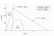
도 2는 일반적인 실리콘 광증배관 소자에서 에피택시층 내 전기장의 분포를 나타내는 도면이다.
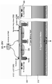
도 3은 본 발명의 일 실시예에 따른 광검출 효율이 향상된 실리콘 광증배관 소자의 단면을 나타내는 도면이다.
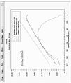
도 4a 및 도 4b는 종래 실리콘 광증배관 소자의 경우 유효 광전류를 나타내는 그래프이다.
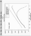
도 5는 본 발명의 일 실시예에 따른 광검출 효율이 향상된 실리콘 광증배관 소자의 경우 유효 광전류를 나타내는 그래프이다.
230: PN 접합층 240: 절연층
250: 저항 260: 알루미늄 구성
270: 트랜치 280: 가드링
Claims (5)
- 다수의 마이크로 픽셀로 이루어진 실리콘 광증배관 소자(Silicon Photomultiplier)에 있어서,
상기 마이크로 픽셀은
p 전도성 타입 또는 n 전도성 타입의 실리콘 기판;
상기 기판 위에 형성되는 상기 기판과 동일한 전도성 타입의 에피텍시층;
상기 에피텍시층 내에 형성되는 PN 접합층; 및
상기 PN 접합층에서 발생하는 유효 광전류를 증가시키도록 상기 PN 접합층 위에 실리콘 질화막으로 형성되는 절연층을 포함하는
실리콘 광증배관 소자.
- 제 1 항에 있어서,
상기 절연층은 50~200nm의 두께를 가지며 형성되는 실리콘 광증배관 소자.
- 제 1 항에 있어서, 상기 PN 접합층은 상기 마이크로 픽셀에 형성되는 전기장이 상기 기판과 수평이 되도록 형성되는 실리콘 광증배관 소자.
- 제 1 항에 있어서, 상기 PN 접합층은
상기 에피텍시층 내에 1017~1018cm-3의 도핑 농도로 형성되는 상기 기판과 동일한 전도성 타입의 제 1 전도성층; 및
상기 제 1 전도성층 위에 1019~1021cm-3의 도핑 농도로 형성되는 상기 기판과 반대인 전도성 타입의 제 2 전도성층을 포함하는 실리콘 광증배관 소자.
- 다수의 마이크로 픽셀로 이루어진 실리콘 광증배관 소자(Silicon Photomultiplier)에 있어서,
상기 마이크로 픽셀은
1012~1016cm-3의 도핑 농도로 형성되는 p 전도성 타입 또는 n 전도성 타입의 실리콘 기판;
상기 기판의 도핑 농도와 동일한 도핑 농도로 상기 기판 위에 형성되는 상기 기판과 동일한 전도성 타입의 에피텍시층;
상기 에피텍시층 내에 형성되는 PN 접합층; 및
상기 PN 접합층에서 발생하는 유효 광전류를 증가시키도록 상기 PN 접합층 위에 실리콘 질화막으로 형성되는 절연층을 포함하는
실리콘 광증배관 소자.
Priority Applications (1)
| Application Number | Priority Date | Filing Date | Title |
|---|---|---|---|
| KR1020120121290A KR20140055040A (ko) | 2012-10-30 | 2012-10-30 | 광검출 효율이 향상된 실리콘 광증배관 소자 |
Applications Claiming Priority (1)
| Application Number | Priority Date | Filing Date | Title |
|---|---|---|---|
| KR1020120121290A KR20140055040A (ko) | 2012-10-30 | 2012-10-30 | 광검출 효율이 향상된 실리콘 광증배관 소자 |
Publications (1)
| Publication Number | Publication Date |
|---|---|
| KR20140055040A true KR20140055040A (ko) | 2014-05-09 |
Family
ID=50886780
Family Applications (1)
| Application Number | Title | Priority Date | Filing Date |
|---|---|---|---|
| KR1020120121290A Ceased KR20140055040A (ko) | 2012-10-30 | 2012-10-30 | 광검출 효율이 향상된 실리콘 광증배관 소자 |
Country Status (1)
| Country | Link |
|---|---|
| KR (1) | KR20140055040A (ko) |
Cited By (2)
| Publication number | Priority date | Publication date | Assignee | Title |
|---|---|---|---|---|
| KR101707896B1 (ko) * | 2015-10-23 | 2017-02-27 | 국방과학연구소 | 실리콘 광 증배 소자 |
| KR20190109219A (ko) * | 2018-03-15 | 2019-09-25 | 한국전자통신연구원 | 실리콘 포토멀티플라이어 |
-
2012
- 2012-10-30 KR KR1020120121290A patent/KR20140055040A/ko not_active Ceased
Cited By (2)
| Publication number | Priority date | Publication date | Assignee | Title |
|---|---|---|---|---|
| KR101707896B1 (ko) * | 2015-10-23 | 2017-02-27 | 국방과학연구소 | 실리콘 광 증배 소자 |
| KR20190109219A (ko) * | 2018-03-15 | 2019-09-25 | 한국전자통신연구원 | 실리콘 포토멀티플라이어 |
Similar Documents
| Publication | Publication Date | Title |
|---|---|---|
| US9054008B2 (en) | Solar blind ultra violet (UV) detector and fabrication methods of the same | |
| RU2290721C2 (ru) | Кремниевый фотоэлектронный умножитель (варианты) и ячейка для кремниевого фотоэлектронного умножителя | |
| KR100879013B1 (ko) | 매립형 컬렉터를 구비하는 포토트랜지스터 | |
| US20100327387A1 (en) | Avalanche Photodiode | |
| JP2015041746A (ja) | シングルフォトンアバランシェダイオード | |
| CN103904152B (zh) | 光电探测器及其制造方法和辐射探测器 | |
| US8212327B2 (en) | High fill-factor laser-treated semiconductor device on bulk material with single side contact scheme | |
| CN108807567A (zh) | 一种可调制表面能带的碲镉汞雪崩二极管探测器 | |
| CN107895743B (zh) | 单光子雪崩光电二极管探测器的装置和方法 | |
| EP0589024A1 (en) | Low capacitance x-ray radiation detector | |
| US10418402B2 (en) | Near ultraviolet photocell | |
| CN117239000B (zh) | 一种雪崩光电二极管及其制作方法、单光子探测器 | |
| KR20180035327A (ko) | 광검출 효율이 향상된 실리콘 광증배관 소자 | |
| KR102284627B1 (ko) | 수광반도체 소자 및 그 제조방법 | |
| KR20140055040A (ko) | 광검출 효율이 향상된 실리콘 광증배관 소자 | |
| KR101638545B1 (ko) | 누설전류를 방지하는 실리콘 광증배관 소자 | |
| US20230369378A1 (en) | Photodiode and manufacturing method thereof | |
| US10121819B2 (en) | Phototransistor having E-B junction and B-C junction are in direct physical contact and completely encapsulated only by the emitter, the collector and a dielectric | |
| US12009439B2 (en) | Photodiode and method for operating a photodiode | |
| US20180337210A1 (en) | Photodetection device which has an inter-diode array and is overdoped by metal diffusion and manufacturing method | |
| KR101707896B1 (ko) | 실리콘 광 증배 소자 | |
| KR101707897B1 (ko) | 실리콘 광 증배 소자 | |
| CN109904271A (zh) | 光传感半导体单元和光传感半导体阵列 | |
| KR20140055029A (ko) | 크로스토크를 감소시키는 실리콘 광증배관 소자 | |
| WO2023069916A1 (en) | Buried photodetector with hetero structure as a gate |
Legal Events
| Date | Code | Title | Description |
|---|---|---|---|
| A201 | Request for examination | ||
| PA0109 | Patent application |
Patent event code: PA01091R01D Comment text: Patent Application Patent event date: 20121030 |
|
| PA0201 | Request for examination | ||
| N231 | Notification of change of applicant | ||
| PN2301 | Change of applicant |
Patent event date: 20131114 Comment text: Notification of Change of Applicant Patent event code: PN23011R01D |
|
| E902 | Notification of reason for refusal | ||
| PE0902 | Notice of grounds for rejection |
Comment text: Notification of reason for refusal Patent event date: 20131216 Patent event code: PE09021S01D |
|
| PG1501 | Laying open of application | ||
| E601 | Decision to refuse application | ||
| PE0601 | Decision on rejection of patent |
Patent event date: 20140627 Comment text: Decision to Refuse Application Patent event code: PE06012S01D Patent event date: 20131216 Comment text: Notification of reason for refusal Patent event code: PE06011S01I |