KR20140107123A - 표시 장치, 표시 장치의 제조 방법, 표시 장치의 구동 방법 및 전자 기기 - Google Patents
표시 장치, 표시 장치의 제조 방법, 표시 장치의 구동 방법 및 전자 기기 Download PDFInfo
- Publication number
- KR20140107123A KR20140107123A KR1020140016591A KR20140016591A KR20140107123A KR 20140107123 A KR20140107123 A KR 20140107123A KR 1020140016591 A KR1020140016591 A KR 1020140016591A KR 20140016591 A KR20140016591 A KR 20140016591A KR 20140107123 A KR20140107123 A KR 20140107123A
- Authority
- KR
- South Korea
- Prior art keywords
- light
- light emitting
- display device
- light receiving
- substrate
- Prior art date
- Legal status (The legal status is an assumption and is not a legal conclusion. Google has not performed a legal analysis and makes no representation as to the accuracy of the status listed.)
- Withdrawn
Links
Images



















Classifications
-
- G—PHYSICS
- G09—EDUCATION; CRYPTOGRAPHY; DISPLAY; ADVERTISING; SEALS
- G09G—ARRANGEMENTS OR CIRCUITS FOR CONTROL OF INDICATING DEVICES USING STATIC MEANS TO PRESENT VARIABLE INFORMATION
- G09G3/00—Control arrangements or circuits, of interest only in connection with visual indicators other than cathode-ray tubes
- G09G3/20—Control arrangements or circuits, of interest only in connection with visual indicators other than cathode-ray tubes for presentation of an assembly of a number of characters, e.g. a page, by composing the assembly by combination of individual elements arranged in a matrix no fixed position being assigned to or needed to be assigned to the individual characters or partial characters
- G09G3/22—Control arrangements or circuits, of interest only in connection with visual indicators other than cathode-ray tubes for presentation of an assembly of a number of characters, e.g. a page, by composing the assembly by combination of individual elements arranged in a matrix no fixed position being assigned to or needed to be assigned to the individual characters or partial characters using controlled light sources
- G09G3/30—Control arrangements or circuits, of interest only in connection with visual indicators other than cathode-ray tubes for presentation of an assembly of a number of characters, e.g. a page, by composing the assembly by combination of individual elements arranged in a matrix no fixed position being assigned to or needed to be assigned to the individual characters or partial characters using controlled light sources using electroluminescent panels
- G09G3/32—Control arrangements or circuits, of interest only in connection with visual indicators other than cathode-ray tubes for presentation of an assembly of a number of characters, e.g. a page, by composing the assembly by combination of individual elements arranged in a matrix no fixed position being assigned to or needed to be assigned to the individual characters or partial characters using controlled light sources using electroluminescent panels semiconductive, e.g. using light-emitting diodes [LED]
- G09G3/3208—Control arrangements or circuits, of interest only in connection with visual indicators other than cathode-ray tubes for presentation of an assembly of a number of characters, e.g. a page, by composing the assembly by combination of individual elements arranged in a matrix no fixed position being assigned to or needed to be assigned to the individual characters or partial characters using controlled light sources using electroluminescent panels semiconductive, e.g. using light-emitting diodes [LED] organic, e.g. using organic light-emitting diodes [OLED]
- G09G3/3225—Control arrangements or circuits, of interest only in connection with visual indicators other than cathode-ray tubes for presentation of an assembly of a number of characters, e.g. a page, by composing the assembly by combination of individual elements arranged in a matrix no fixed position being assigned to or needed to be assigned to the individual characters or partial characters using controlled light sources using electroluminescent panels semiconductive, e.g. using light-emitting diodes [LED] organic, e.g. using organic light-emitting diodes [OLED] using an active matrix
-
- G—PHYSICS
- G09—EDUCATION; CRYPTOGRAPHY; DISPLAY; ADVERTISING; SEALS
- G09G—ARRANGEMENTS OR CIRCUITS FOR CONTROL OF INDICATING DEVICES USING STATIC MEANS TO PRESENT VARIABLE INFORMATION
- G09G2320/00—Control of display operating conditions
- G09G2320/02—Improving the quality of display appearance
- G09G2320/0233—Improving the luminance or brightness uniformity across the screen
-
- G—PHYSICS
- G09—EDUCATION; CRYPTOGRAPHY; DISPLAY; ADVERTISING; SEALS
- G09G—ARRANGEMENTS OR CIRCUITS FOR CONTROL OF INDICATING DEVICES USING STATIC MEANS TO PRESENT VARIABLE INFORMATION
- G09G2320/00—Control of display operating conditions
- G09G2320/04—Maintaining the quality of display appearance
- G09G2320/043—Preventing or counteracting the effects of ageing
- G09G2320/046—Dealing with screen burn-in prevention or compensation of the effects thereof
-
- G—PHYSICS
- G09—EDUCATION; CRYPTOGRAPHY; DISPLAY; ADVERTISING; SEALS
- G09G—ARRANGEMENTS OR CIRCUITS FOR CONTROL OF INDICATING DEVICES USING STATIC MEANS TO PRESENT VARIABLE INFORMATION
- G09G2360/00—Aspects of the architecture of display systems
- G09G2360/14—Detecting light within display terminals, e.g. using a single or a plurality of photosensors
- G09G2360/141—Detecting light within display terminals, e.g. using a single or a plurality of photosensors the light conveying information used for selecting or modulating the light emitting or modulating element
- G09G2360/142—Detecting light within display terminals, e.g. using a single or a plurality of photosensors the light conveying information used for selecting or modulating the light emitting or modulating element the light being detected by light detection means within each pixel
-
- G—PHYSICS
- G09—EDUCATION; CRYPTOGRAPHY; DISPLAY; ADVERTISING; SEALS
- G09G—ARRANGEMENTS OR CIRCUITS FOR CONTROL OF INDICATING DEVICES USING STATIC MEANS TO PRESENT VARIABLE INFORMATION
- G09G2360/00—Aspects of the architecture of display systems
- G09G2360/14—Detecting light within display terminals, e.g. using a single or a plurality of photosensors
- G09G2360/145—Detecting light within display terminals, e.g. using a single or a plurality of photosensors the light originating from the display screen
- G09G2360/147—Detecting light within display terminals, e.g. using a single or a plurality of photosensors the light originating from the display screen the originated light output being determined for each pixel
- G09G2360/148—Detecting light within display terminals, e.g. using a single or a plurality of photosensors the light originating from the display screen the originated light output being determined for each pixel the light being detected by light detection means within each pixel
-
- Y—GENERAL TAGGING OF NEW TECHNOLOGICAL DEVELOPMENTS; GENERAL TAGGING OF CROSS-SECTIONAL TECHNOLOGIES SPANNING OVER SEVERAL SECTIONS OF THE IPC; TECHNICAL SUBJECTS COVERED BY FORMER USPC CROSS-REFERENCE ART COLLECTIONS [XRACs] AND DIGESTS
- Y10—TECHNICAL SUBJECTS COVERED BY FORMER USPC
- Y10T—TECHNICAL SUBJECTS COVERED BY FORMER US CLASSIFICATION
- Y10T29/00—Metal working
- Y10T29/49—Method of mechanical manufacture
Landscapes
- Engineering & Computer Science (AREA)
- Physics & Mathematics (AREA)
- Computer Hardware Design (AREA)
- General Physics & Mathematics (AREA)
- Theoretical Computer Science (AREA)
- Electroluminescent Light Sources (AREA)
- Devices For Indicating Variable Information By Combining Individual Elements (AREA)
- Control Of Indicators Other Than Cathode Ray Tubes (AREA)
- Control Of El Displays (AREA)
Abstract
Description
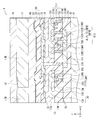
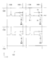
도 2는 도 1에 도시한 표시 장치의 전체 구성을 도시하는 도면.
도 3은 도 2에 도시한 화소 구동 회로의 한 예를 도시하는 도면.
도 4는 도 1에 도시한 표시 장치의 보정 회로를 설명하기 위한 블록도.
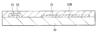
도 5a는 도 1에 도시한 표시 장치의 제조 공정(기판측)을 도시하는 단면도.
도 5b는 도 5a에 계속된 공정을 도시하는 단면도.
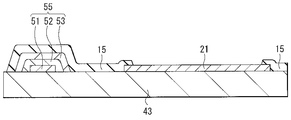
도 5c는 도 5b에 계속된 공정을 도시하는 단면도.
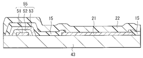
도 5d는 도 5c에 계속된 공정을 도시하는 단면도.
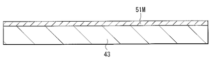
도 6a는 도 1에 도시한 표시 장치의 제조 공정(대향 기판측)을 도시하는 단면도.
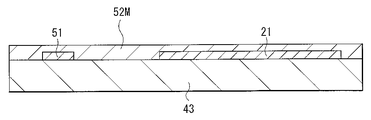
도 6b는 도 6a에 계속된 공정을 도시하는 단면도.
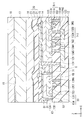
도 7은 도 1에 도시한 표시 장치의 동작을 도시하는 단면도.
도 8은 도 1에 도시한 표시 장치의 휘도 보정 동작에 관해 설명하기 위한 도면.
도 9는 비교예에 관한 표시 장치의 구성을 도시하는 단면도.
도 10은 도 1에 도시한 표시 장치의 다른 예를 도시하는 단면도.
도 11은 변형예 1에 관한 표시 장치의 구성을 도시하는 단면도.
도 12는 도 11에 도시한 반사부의 작용에 관해 설명하기 위한 단면도.
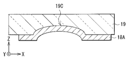
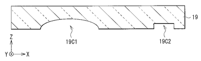
도 13은 도 11에 도시한 반사부의 형성 방법의 한 예를 도시하는 단면도.
도 14는 도 11에 도시한 반사부의 형성 방법의 다른 예를 도시하는 단면도.
도 15는 도 13, 도 14에 도시한 반사부의 형성 방법에 관해 설명하기 위한 단면도.
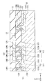
도 16은 본 기술의 제2의 실시의 형태에 관한 표시 장치의 구성을 도시하는 단면도.
도 17a는 도 16에 도시한 차폐부의 단면 구성의 다른 예를 도시하는 도면.
도 17b는 도 16에 도시한 차폐부의 단면 구성의 그 밖의 예를 도시하는 도면.
도 18a는 도 16에 도시한 차폐부의 평면 구성의 제1예를 도시하는 도면.
도 18b는 도 16에 도시한 차폐부의 제2예를 도시하는 평면도.
도 18c는 도 16에 도시한 차폐부의 제3예를 도시하는 평면도.
도 18d는 도 16에 도시한 차폐부의 제4예를 도시하는 평면도.
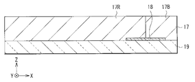
도 19는 도 16에 도시한 차폐부의 작용에 관해 설명하기 위한 단면도.
도 20은 도 16에 도시한 표시 장치의 제조 공정의 한 예를 도시하는 단면도.
도 21은 변형예 2에 관한 표시 장치의 구성을 도시하는 단면도.
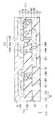
도 22는 본 기술의 제3의 실시의 형태에 관한 표시 장치의 주요부의 구성을 도시하는 단면도.
도 23a는 도 22에 도시한 표시 장치의 제조 공정의 한 예를 도시하는 단면도.
도 23b는 도 23a에 계속된 공정을 도시하는 단면도.
도 23c는 도 23b에 계속된 공정을 도시하는 단면도.
도 24a는 도 23c에 계속된 공정을 도시하는 단면도.
도 24b는 도 24a에 계속된 공정을 도시하는 단면도.
도 24c는 도 24b에 계속된 공정을 도시하는 단면도.
도 25a는 도 24c에 계속된 공정을 도시하는 단면도.
도 25b는 도 25a에 계속된 공정을 도시하는 단면도.
도 25c는 도 25b에 계속된 공정을 도시하는 단면도.
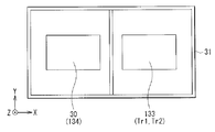
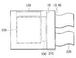
도 26은 도 1 등에 도시한 표시 장치를 포함하는 모듈의 개략 구성을 도시하는 평면도.
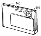
도 27은 적용예 1의 외관을 도시하는 사시도.
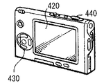
도 28a는 적용예 2의 표측에서 본 외관을 도시하는 사시도.
도 28b는 적용예 2의 이측에서 본 외관을 도시하는 사시도.
도 29는 적용예 3의 외관을 도시하는 사시도.
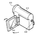
도 30은 적용예 4의 외관을 도시하는 사시도.
도 31a는 적용예 5의 닫은 상태를 도시하는 도면.
도 31b는 적용예 5의 연 상태를 도시하는 도면.

10 : 화소
11 : 지지 부재
12 : 다층 배선층
13, 43 : 기판
13a : Si층
13b : 절연층
43a : 판형상 부재
43b : TFT층
13V : 관통 전극
13W1, 13W2, 13W3, 13W4, 13W5, 13W6, 13W7 : 도전성 플러그
Tr1, Tr2, Tr3 : 트랜지스터
TG1, TG2, TG3 : 게이트 전극
14 : 절연층
15 : 소자 분리층
16 : 보호층
17 : CF층
18, 18a : 반사부
19 : 대향 기판
20 : 발광부
21 : 제1 전극
22 : 유기층
23 : 제2 전극
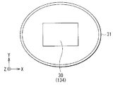
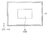
30, 50 : 수광부
31, 32 : 차폐부
Claims (20)
- 표시 장치에 있어서,
표시 영역 내에 발광부와,
상기 발광부로부터의 광을 수광하는 수광부를 갖는 것을 특징으로 하는 표시 장치. - 제 1항에 있어서,
상기 발광부를 구동하는 화소 구동 회로와,
상기 수광부의 수광량에 응하여 상기 화소 구동 회로에 보정 신호를 보내는 보정 회로를 더 구비하는 것을 특징으로 하는 표시 장치. - 제 2항에 있어서,
상기 발광부 및 상기 수광부는, 기판의 표면에 마련되어 있는 것을 특징으로 하는 표시 장치. - 제 3항에 있어서,
상기 수광부는, 한 쌍의 전극의 사이에 광전 변환막을 갖고 있는 것을 특징으로 하는 표시 장치. - 제 2항에 있어서,
상기 발광부는 기판의 표면에 마련되고,
상기 수광부는 상기 기판의 내부에 마련되어 있는 것을 특징으로 하는 표시 장치. - 제 5항에 있어서,
상기 수광부는 포토 다이오드에 의해 구성되어 있는 것을 특징으로 하는 표시 장치. - 제 5항에 있어서,
상기 기판은 실리콘층을 갖는 것을 특징으로 하는 표시 장치. - 제 7항에 있어서,
상기 실리콘층의 이면 부근에 상기 수광부가 마련되어 있는 것을 특징으로 하는 표시 장치. - 제 5항에 있어서,
상기 화소 구동 회로는 트랜지스터를 포함하고, 상기 트랜지스터가 상기 발광부와 평면시에서 겹쳐지는 위치에 마련되어 있는 것을 특징으로 하는 표시 장치. - 제 9항에 있어서,
상기 트랜지스터 및 상기 수광부를 화소마다 가지며, 상기 트랜지스터와 상기 수광부는 서로 이웃하는 위치에 마련되어 있는 것을 특징으로 하는 표시 장치. - 제 10항에 있어서,
상기 트랜지스터와 상기 수광부와의 사이에 차폐부를 갖는 것을 특징으로 하는 표시 장치. - 제 11항에 있어서,
상기 차폐부는, 상기 기판의 홈에 매설된 절연막인 것을 특징으로 하는 표시 장치. - 제 11항에 있어서,
상기 차폐부는, 상기 기판의 홈에 매설된 금속막인 것을 특징으로 하는 표시 장치. - 제 11항에 있어서,
상기 차폐부는, 상기 기판의 홈에 매설된 구리인 것을 특징으로 하는 표시 장치. - 제 11항에 있어서,
상기 수광부를 둘러싸도록 상기 차폐부가 마련되어 있는 것을 특징으로 하는 표시 장치. - 제 5항에 있어서,
상기 기판과 대향하는 반사부를 가지며, 상기 반사부에서 반사된 상기 발광부로부터의 광이 상기 수광부에 입사하는 것을 특징으로 하는 표시 장치. - 제 16항에 있어서,
상기 반사부의 상기 기판과의 대향면은 포물곡면인 것을 특징으로 하는 표시 장치. - 전자 기기에 있어서,
표시 장치를 구비하고,
상기 표시 장치는, 표시 영역 내에 발광부와,
상기 발광부로부터의 광을 수광하는 수광부를 갖는 것을 특징으로 하는 전자 기기. - 표시 장치의 구동 방법에 있어서,
화소 구동 회로에 의해 표시 영역 내의 발광부를 구동하고,
상기 발광부로부터의 광을 상기 표시 영역 내의 수광부에서 수광하고,
상기 수광부의 수광량에 응하여 보정 회로로부터 상기 화소 구동 회로에 보정 신호를 보내는 것을 특징으로 하는 표시 장치의 구동 방법. - 표시 장치의 제조 방법에 있어서,
표시 영역 내에 발광부와,
상기 발광부로부터의 광을 수광하는 수광부를 형성하는 것을 특징으로 하는 표시 장치의 제조 방법.
Applications Claiming Priority (4)
| Application Number | Priority Date | Filing Date | Title |
|---|---|---|---|
| JPJP-P-2013-037375 | 2013-02-27 | ||
| JP2013037375 | 2013-02-27 | ||
| JP2013159320A JP2014194517A (ja) | 2013-02-27 | 2013-07-31 | 表示装置、表示装置の製造方法、表示装置の駆動方法および電子機器 |
| JPJP-P-2013-159320 | 2013-07-31 |
Publications (1)
| Publication Number | Publication Date |
|---|---|
| KR20140107123A true KR20140107123A (ko) | 2014-09-04 |
Family
ID=51369649
Family Applications (1)
| Application Number | Title | Priority Date | Filing Date |
|---|---|---|---|
| KR1020140016591A Withdrawn KR20140107123A (ko) | 2013-02-27 | 2014-02-13 | 표시 장치, 표시 장치의 제조 방법, 표시 장치의 구동 방법 및 전자 기기 |
Country Status (4)
| Country | Link |
|---|---|
| US (1) | US20140240370A1 (ko) |
| JP (1) | JP2014194517A (ko) |
| KR (1) | KR20140107123A (ko) |
| CN (1) | CN104009060A (ko) |
Cited By (1)
| Publication number | Priority date | Publication date | Assignee | Title |
|---|---|---|---|---|
| KR20190098883A (ko) * | 2018-02-14 | 2019-08-23 | 삼성디스플레이 주식회사 | 표시 장치 |
Families Citing this family (16)
| Publication number | Priority date | Publication date | Assignee | Title |
|---|---|---|---|---|
| KR20210068638A (ko) * | 2014-10-28 | 2021-06-09 | 가부시키가이샤 한도오따이 에네루기 켄큐쇼 | 발광 장치 |
| KR102363429B1 (ko) * | 2015-02-02 | 2022-02-17 | 삼성디스플레이 주식회사 | 유기 발광 표시 장치 |
| JP2017174936A (ja) * | 2016-03-23 | 2017-09-28 | ソニー株式会社 | 固体撮像素子及び電子機器 |
| US9961178B2 (en) | 2016-03-24 | 2018-05-01 | Motorola Mobility Llc | Embedded active matrix organic light emitting diode (AMOLED) fingerprint sensor |
| US20170289805A1 (en) * | 2016-03-30 | 2017-10-05 | Motorola Mobility Llc | Embedded active matrix organic light emitting diode (amoled) fingerprint sensor and self-compensating amoled |
| CN107393863A (zh) * | 2017-05-22 | 2017-11-24 | 茆胜 | Oled微型显示器ic片及其制备方法 |
| CN107342375B (zh) * | 2017-08-21 | 2019-05-31 | 深圳市华星光电半导体显示技术有限公司 | 柔性显示面板的制作方法及柔性显示面板 |
| DE112018005383T5 (de) * | 2017-09-22 | 2020-06-18 | Sony Corporation | Anzeigeelement, anzeigevorrichtung und elektronische vorrichtung |
| CN111261106A (zh) * | 2018-11-30 | 2020-06-09 | 京东方科技集团股份有限公司 | 显示面板及其制作方法、像素发光补偿方法以及显示装置 |
| CN109638047B (zh) | 2018-12-13 | 2020-12-22 | 京东方科技集团股份有限公司 | 显示面板及其制作方法和驱动显示面板的方法 |
| CN110265442B (zh) * | 2019-06-14 | 2021-04-02 | 京东方科技集团股份有限公司 | 显示基板及包含其的显示面板 |
| CN111524943A (zh) * | 2020-04-27 | 2020-08-11 | 武汉华星光电半导体显示技术有限公司 | 显示面板和显示装置 |
| WO2021225139A1 (ja) * | 2020-05-08 | 2021-11-11 | ソニーグループ株式会社 | 表示装置および電子機器 |
| CN113725379B (zh) * | 2020-05-25 | 2022-12-09 | 京东方科技集团股份有限公司 | 显示模组和显示装置 |
| JP7510820B2 (ja) * | 2020-08-31 | 2024-07-04 | シャープ福山レーザー株式会社 | 画像表示素子 |
| JP7780273B2 (ja) * | 2021-08-26 | 2025-12-04 | キヤノン株式会社 | 表示装置、光電変換装置、電子機器、照明装置、移動体、および、ウェアラブルデバイス |
Family Cites Families (4)
| Publication number | Priority date | Publication date | Assignee | Title |
|---|---|---|---|---|
| JP2005159137A (ja) * | 2003-11-27 | 2005-06-16 | Sharp Corp | 光半導体素子およびこの光半導体素子を用いた電子機器 |
| GB0406107D0 (en) * | 2004-03-17 | 2004-04-21 | Koninkl Philips Electronics Nv | Electroluminescent display devices |
| KR100759681B1 (ko) * | 2006-03-29 | 2007-09-17 | 삼성에스디아이 주식회사 | 유기 전계 발광표시장치 |
| JP5310372B2 (ja) * | 2009-08-12 | 2013-10-09 | ソニー株式会社 | 表示装置、輝度劣化補正方法および電子機器 |
-
2013
- 2013-07-31 JP JP2013159320A patent/JP2014194517A/ja active Pending
-
2014
- 2014-02-10 US US14/176,656 patent/US20140240370A1/en not_active Abandoned
- 2014-02-13 KR KR1020140016591A patent/KR20140107123A/ko not_active Withdrawn
- 2014-02-20 CN CN201410058610.7A patent/CN104009060A/zh active Pending
Cited By (1)
| Publication number | Priority date | Publication date | Assignee | Title |
|---|---|---|---|---|
| KR20190098883A (ko) * | 2018-02-14 | 2019-08-23 | 삼성디스플레이 주식회사 | 표시 장치 |
Also Published As
| Publication number | Publication date |
|---|---|
| CN104009060A (zh) | 2014-08-27 |
| US20140240370A1 (en) | 2014-08-28 |
| JP2014194517A (ja) | 2014-10-09 |
Similar Documents
| Publication | Publication Date | Title |
|---|---|---|
| KR20140107123A (ko) | 표시 장치, 표시 장치의 제조 방법, 표시 장치의 구동 방법 및 전자 기기 | |
| CN109994522B (zh) | 显示装置 | |
| KR102323630B1 (ko) | 표시 장치 및 그 제조 방법, 및 전자 기기의 제조 방법 | |
| EP2207219B1 (en) | Organic light emitting diode display and method of manufacturing the same | |
| US8963170B2 (en) | Organic light emitting device and display unit including the same | |
| US8415675B2 (en) | Organic light emitting display device and method of fabricating the same | |
| CN102956712B (zh) | 显示器、制造显示器的方法以及电子设备 | |
| EP2816627B1 (en) | Display device | |
| US20150379924A1 (en) | Pixel array, metal mask, electro optical device and electric apparatus | |
| US10128324B2 (en) | Method of manufacturing display unit with a second electrode formed to extend across a bezel region | |
| KR20140140484A (ko) | 표시 장치 및 표시 장치의 제조 방법 및 전자 기기 | |
| KR20180004384A (ko) | 유기 발광 표시 장치 및 유기 발광 표시 장치의 제조 방법 | |
| US12127443B2 (en) | Display device and method of manufacturing the same | |
| KR20170049659A (ko) | 유기 발광 표시 장치 | |
| KR20150018030A (ko) | 유기 발광 표시 장치 | |
| US20170033170A1 (en) | Organic light emitting diode display | |
| KR20160089011A (ko) | 유기 발광 표시 장치 | |
| KR20160092110A (ko) | 유기 발광 표시 장치 | |
| US10312471B2 (en) | Method of manufacturing display device, display device, and electronic device | |
| KR101511548B1 (ko) | 발광표시장치 및 이의 제조방법 | |
| KR102381901B1 (ko) | 표시 장치 및 이의 제조 방법 | |
| JP2014049405A (ja) | 表示装置およびその製造方法、並びに電子機器 | |
| KR101383490B1 (ko) | 전계발광소자 | |
| KR102847530B1 (ko) | 표시 장치 및 표시 장치의 제조 방법 | |
| KR100669774B1 (ko) | 평판표시장치 및 그의 제조방법 |
Legal Events
| Date | Code | Title | Description |
|---|---|---|---|
| PA0109 | Patent application |
St.27 status event code: A-0-1-A10-A12-nap-PA0109 |
|
| P11-X000 | Amendment of application requested |
St.27 status event code: A-2-2-P10-P11-nap-X000 |
|
| P13-X000 | Application amended |
St.27 status event code: A-2-2-P10-P13-nap-X000 |
|
| R15-X000 | Change to inventor requested |
St.27 status event code: A-3-3-R10-R15-oth-X000 |
|
| R16-X000 | Change to inventor recorded |
St.27 status event code: A-3-3-R10-R16-oth-X000 |
|
| PG1501 | Laying open of application |
St.27 status event code: A-1-1-Q10-Q12-nap-PG1501 |
|
| N231 | Notification of change of applicant | ||
| PN2301 | Change of applicant |
St.27 status event code: A-3-3-R10-R13-asn-PN2301 St.27 status event code: A-3-3-R10-R11-asn-PN2301 |
|
| PC1203 | Withdrawal of no request for examination |
St.27 status event code: N-1-6-B10-B12-nap-PC1203 |
|
| WITN | Application deemed withdrawn, e.g. because no request for examination was filed or no examination fee was paid | ||
| P22-X000 | Classification modified |
St.27 status event code: A-2-2-P10-P22-nap-X000 |
|
| R18-X000 | Changes to party contact information recorded |
St.27 status event code: A-3-3-R10-R18-oth-X000 |