KR20140141993A - 와이어 본딩 기계의 동작 조건 오류 검출 방법 및 이를 수행하기 위한 장치 - Google Patents
와이어 본딩 기계의 동작 조건 오류 검출 방법 및 이를 수행하기 위한 장치 Download PDFInfo
- Publication number
- KR20140141993A KR20140141993A KR20130063471A KR20130063471A KR20140141993A KR 20140141993 A KR20140141993 A KR 20140141993A KR 20130063471 A KR20130063471 A KR 20130063471A KR 20130063471 A KR20130063471 A KR 20130063471A KR 20140141993 A KR20140141993 A KR 20140141993A
- Authority
- KR
- South Korea
- Prior art keywords
- conductive wires
- wire bonding
- bonding machine
- operating conditions
- actual
- Prior art date
- Legal status (The legal status is an assumption and is not a legal conclusion. Google has not performed a legal analysis and makes no representation as to the accuracy of the status listed.)
- Granted
Links
Images


Classifications
-
- G—PHYSICS
- G01—MEASURING; TESTING
- G01R—MEASURING ELECTRIC VARIABLES; MEASURING MAGNETIC VARIABLES
- G01R31/00—Arrangements for testing electric properties; Arrangements for locating electric faults; Arrangements for electrical testing characterised by what is being tested not provided for elsewhere
- G01R31/50—Testing of electric apparatus, lines, cables or components for short-circuits, continuity, leakage current or incorrect line connections
- G01R31/66—Testing of connections, e.g. of plugs or non-disconnectable joints
-
- H—ELECTRICITY
- H10—SEMICONDUCTOR DEVICES; ELECTRIC SOLID-STATE DEVICES NOT OTHERWISE PROVIDED FOR
- H10P—GENERIC PROCESSES OR APPARATUS FOR THE MANUFACTURE OR TREATMENT OF DEVICES COVERED BY CLASS H10
- H10P74/00—Testing or measuring during manufacture or treatment of wafers, substrates or devices
-
- G—PHYSICS
- G06—COMPUTING OR CALCULATING; COUNTING
- G06F—ELECTRIC DIGITAL DATA PROCESSING
- G06F11/00—Error detection; Error correction; Monitoring
- G06F11/22—Detection or location of defective computer hardware by testing during standby operation or during idle time, e.g. start-up testing
- G06F11/26—Functional testing
-
- G—PHYSICS
- G01—MEASURING; TESTING
- G01R—MEASURING ELECTRIC VARIABLES; MEASURING MAGNETIC VARIABLES
- G01R31/00—Arrangements for testing electric properties; Arrangements for locating electric faults; Arrangements for electrical testing characterised by what is being tested not provided for elsewhere
- G01R31/50—Testing of electric apparatus, lines, cables or components for short-circuits, continuity, leakage current or incorrect line connections
-
- G—PHYSICS
- G01—MEASURING; TESTING
- G01R—MEASURING ELECTRIC VARIABLES; MEASURING MAGNETIC VARIABLES
- G01R31/00—Arrangements for testing electric properties; Arrangements for locating electric faults; Arrangements for electrical testing characterised by what is being tested not provided for elsewhere
- G01R31/50—Testing of electric apparatus, lines, cables or components for short-circuits, continuity, leakage current or incorrect line connections
- G01R31/52—Testing for short-circuits, leakage current or ground faults
Landscapes
- Engineering & Computer Science (AREA)
- Physics & Mathematics (AREA)
- General Physics & Mathematics (AREA)
- General Engineering & Computer Science (AREA)
- Theoretical Computer Science (AREA)
- Computer Hardware Design (AREA)
- Quality & Reliability (AREA)
- Wire Bonding (AREA)
- Automation & Control Theory (AREA)
Abstract
Description
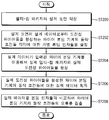
도 2는 도 1의 장치를 이용해서 와이어 본딩 기계의 동작 조건 오류를 검출하는 방법을 순차적으로 나타낸 흐름도이다.
도 3은 본 발명의 다른 실시예에 따른 와이어 본딩 기계의 동작 조건 오류 검출 장치를 나타낸 블럭도이다.
도 4는 도 3의 장치가 도전성 와이어들을 그룹핑하는 동작을 나타낸 사시도이다.
도 5는 도 3의 장치를 이용해서 와이어 본딩 기계의 동작 조건 오류를 검출하는 방법을 순차적으로 나타낸 흐름도이다.
C1 ; 제 1 반도체 칩 C2 ; 제 2 반도체 칩
CP1 ; 제 1 패드 CP2 ; 제 2 패드
WG1 ; 제 1 도전성 와이어 WG2 ; 제 2 도전성 와이어
WG2-1 ; 제 2 중앙 도전성 와이어
WG2-2 ; 제 2 가장자리 도전성 와이어
Claims (10)
- 반도체 패키지의 반도체 칩들을 전기적으로 연결시키는 도전성 와이어들에 대한 정보를 포함하는 설계 데이터로부터 상기 도전성 와이어들을 형성하는 와이어 본딩 기계의 동작 조건들 각각에 대한 개별 본딩 인자(bond parameter)들을 설정하는 단계;
상기 설계 데이터가 입력된 상기 와이어 본딩 기계를 이용해서 실제 반도체 패키지의 실제 도전성 와이어들을 형성하는 단계;
상기 실제 도전성 와이어들을 형성한 상기 와이어 본딩 기계의 동작 조건들에 대한 실제 데이터를 획득하는 단계; 및
상기 실제 데이터를 상기 본딩 인자들과 비교하여, 상기 와이어 본딩 기계의 동작 조건의 오류를 검출하는 와이어 본딩 기계의 동작 조건 오류 검출 방법. - 제 1 항에 있어서, 상기 설계 데이터에서 상기 도전성 와이어들을 동일한 전기적 연결 기능을 갖는 도전성 와이어들로 그룹핑(grouping)하는 단계를 더 포함하는 와이어 본딩 기계의 동작 조건 오류 검출 방법.
- 제 2 항에 있어서, 상기 본딩 인자들을 설정하는 단계는
상기 그룹핑된 도전성 와이어들을 형성하는 상기 와이어 본딩 기계의 동작 조건들 각각에 대한 그룹별 본딩 인자들을 설정하는 단계를 포함하는 와이어 본딩 기계의 동작 조건 오류 검출 방법. - 제 2 항에 있어서, 상기 도전성 와이어들을 상기 동일한 전기적 연결 기능을 갖는 상기 도전성 와이어들로 그룹핑하는 단계는
상기 도전성 와이어들을 상기 반도체 칩들에 동일한 입출력 신호를 부여하도록 상기 반도체 칩들을 연결하는 상기 도전성 와이어들로 1차 그룹핑하는 단계를 포함하는 와이어 본딩 기계의 동작 조건 오류 검출 방법. - 제 4 항에 있어서, 상기 1차 그룹핑된 도전성 와이어들 각각을 동일한 루프(loop) 궤적을 갖는 도전성 와이어들로 2차 그룹핑하는 단계를 더 포함하는 와이어 본딩 기계의 동작 조건 오류 검출 방법.
- 제 5 항에 있어서, 상기 본딩 인자들을 설정하는 단계는
상기 1차 그룹핑된 도전성 와이어들을 형성하는 상기 와이어 본딩 기계의 동작 조건들 각각에 대한 1차 그룹별 본딩 인자들을 설정하는 단계; 및
상기 2차 그룹핑된 도전성 와이어들을 형성하는 상기 와이어 본딩 기계의 동작 조건들 각각에 대한 2차 그룹별 본딩 인자들을 설정하는 단계를 포함하는 와이어 본딩 기계의 동작 조건 오류 검출 방법. - 제 1 항에 있어서, 상기 본딩 인자들은 상기 와이어 본딩 기계가 상기 도전성 와이어 형성에 사용되는 전류, 힘 및 시간을 포함하는 와이어 본딩 기계의 동작 조건 오류 검출 방법.
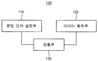
- 반도체 패키지의 반도체 칩들을 전기적으로 연결시키는 도전성 와이어들에 대한 정보를 포함하는 설계 데이터로부터 상기 도전성 와이어들을 형성하는 와이어 본딩 기계의 동작 조건들 각각에 대한 개별 본딩 인자(bond parameter)들을 설정하는 본딩 인자 설정부;
상기 설계 데이터를 이용해서 실제 반도체 패키지의 실제 도전성 와이어들을 형성하는 상기 와이어 본딩 기계의 동작 조건들에 대한 실제 데이터를 획득하는 데이터 획득부; 및
상기 실제 데이터를 상기 본딩 인자들과 비교하여, 상기 와이어 본딩 기계의 동작 조건 오류를 검출하는 검출부를 포함하는 와이어 본딩 기계의 동작 조건 오류 검출 장치. - 제 8 항에 있어서, 상기 설계 데이터에서 상기 도전성 와이어들을 동일한 전기적 연결 기능을 갖는 도전성 와이어들로 그룹핑하는 분류부를 더 포함하는 와이어 본딩 기계의 동작 조건 오류 검출 장치.
- 제 9 항에 있어서, 상기 분류부는
상기 도전성 와이어들을 상기 반도체 칩들에 동일한 입출력 신호를 부여하도록 상기 반도체 칩들을 연결하는 상기 도전성 와이어들로 1차 그룹핑하는 1차 분류부; 및
상기 1차 그룹핑된 도전성 와이어들 각각을 동일한 루프(loop) 궤적을 갖는 도전성 와이어들로 2차 그룹핑하는 2차 분류부를 포함하는 와이어 본딩 기계의 동작 조건 오류 검출 장치.
Priority Applications (2)
| Application Number | Priority Date | Filing Date | Title |
|---|---|---|---|
| KR1020130063471A KR102127892B1 (ko) | 2013-06-03 | 2013-06-03 | 와이어 본딩 기계의 동작 조건 오류 검출 방법 및 이를 수행하기 위한 장치 |
| US14/185,447 US9384105B2 (en) | 2013-06-03 | 2014-02-20 | Method of detecting faults of operation algorithms in a wire bonding machine and apparatus for performing the same |
Applications Claiming Priority (1)
| Application Number | Priority Date | Filing Date | Title |
|---|---|---|---|
| KR1020130063471A KR102127892B1 (ko) | 2013-06-03 | 2013-06-03 | 와이어 본딩 기계의 동작 조건 오류 검출 방법 및 이를 수행하기 위한 장치 |
Publications (2)
| Publication Number | Publication Date |
|---|---|
| KR20140141993A true KR20140141993A (ko) | 2014-12-11 |
| KR102127892B1 KR102127892B1 (ko) | 2020-06-29 |
Family
ID=51986585
Family Applications (1)
| Application Number | Title | Priority Date | Filing Date |
|---|---|---|---|
| KR1020130063471A Active KR102127892B1 (ko) | 2013-06-03 | 2013-06-03 | 와이어 본딩 기계의 동작 조건 오류 검출 방법 및 이를 수행하기 위한 장치 |
Country Status (2)
| Country | Link |
|---|---|
| US (1) | US9384105B2 (ko) |
| KR (1) | KR102127892B1 (ko) |
Cited By (1)
| Publication number | Priority date | Publication date | Assignee | Title |
|---|---|---|---|---|
| KR20230101372A (ko) * | 2021-12-29 | 2023-07-06 | 주식회사 에스에프에이 | 반도체 와이어본딩 공정 모니터링 장치 및 그 장치의 구동방법 |
Families Citing this family (3)
| Publication number | Priority date | Publication date | Assignee | Title |
|---|---|---|---|---|
| US10170384B2 (en) * | 2017-03-03 | 2019-01-01 | Texas Instruments Incorporated | Methods and apparatus providing a graded package for a semiconductor |
| JP2025510531A (ja) * | 2022-04-06 | 2025-04-15 | クリック アンド ソッファ インダストリーズ、インク. | ワイヤーボンディングアプリケーションに対するワイヤーボンディングツールの適合性を決定する方法、およびその関連方法 |
| WO2025198463A1 (en) * | 2024-03-21 | 2025-09-25 | Mimos Berhad | Method and system for identifying wire bond defect of a semiconductor device |
Citations (2)
| Publication number | Priority date | Publication date | Assignee | Title |
|---|---|---|---|---|
| JP2007129121A (ja) * | 2005-11-07 | 2007-05-24 | Nec Electronics Corp | 半導体チップ組立判定装置 |
| KR20110118928A (ko) * | 2010-04-26 | 2011-11-02 | 주식회사 미라콤아이앤씨 | 와이어본딩 프로세스에서의 오류 자동 검출 방법, 시스템, 및 저장 매체 |
Family Cites Families (15)
| Publication number | Priority date | Publication date | Assignee | Title |
|---|---|---|---|---|
| EP0747930B1 (en) * | 1995-05-19 | 2000-09-27 | STMicroelectronics S.r.l. | Electronic device with multiple bonding wires, method of fabrication and method of testing bonding wire integrity |
| JPH09113566A (ja) | 1995-10-16 | 1997-05-02 | Nissan Motor Co Ltd | 半導体基板の接続状態検出装置 |
| KR20000018709A (ko) | 1998-09-04 | 2000-04-06 | 윤종용 | 볼 그리드 어레이 패키지용 와이어 본딩 설비 및와이어본딩 방법 |
| KR100295415B1 (ko) | 1998-09-15 | 2001-10-26 | 마이클 디. 오브라이언 | 반도체패키지의와이어본딩상태확인방법 |
| JP2000208551A (ja) | 1999-01-19 | 2000-07-28 | Seiko Epson Corp | 半導体組立装置と半導体装置 |
| KR100777862B1 (ko) | 1999-02-02 | 2007-11-21 | 텍사스 인스트루먼츠 인코포레이티드 | 와이어 본딩 및 테스팅을 위한 결합 시스템, 방법 및 장치 |
| US6568581B2 (en) * | 2001-03-15 | 2003-05-27 | Asm Technology Singapore Pte. Ltd. | Detection of wire bonding failures |
| US6789235B1 (en) | 2001-09-05 | 2004-09-07 | National Semiconductor Corporation | Bond program verification system |
| TW513795B (en) | 2001-12-31 | 2002-12-11 | Siliconware Precision Industries Co Ltd | Wire bonding method and system for fabricating semiconductor package |
| KR100442697B1 (ko) | 2002-03-11 | 2004-08-02 | 삼성전자주식회사 | 자동 와이어 본딩 공정을 위한 통합 관리 시스템 |
| US7004373B1 (en) * | 2003-04-07 | 2006-02-28 | West Bond, Inc. | Wire bond fault detection method and apparatus |
| KR20060012466A (ko) | 2004-08-03 | 2006-02-08 | 삼성전자주식회사 | 와이어 본딩 방법 |
| KR100881198B1 (ko) * | 2007-06-20 | 2009-02-05 | 삼성전자주식회사 | 반도체 패키지 및 이를 실장한 반도체 패키지 모듈 |
| KR20090088638A (ko) | 2008-02-15 | 2009-08-20 | 삼성테크윈 주식회사 | 와이어 본딩 공정의 리젝트 데이터 관리방법 |
| CN103730390A (zh) * | 2012-10-15 | 2014-04-16 | 飞思卡尔半导体公司 | 引线接合机以及测试引线接合连接的方法 |
-
2013
- 2013-06-03 KR KR1020130063471A patent/KR102127892B1/ko active Active
-
2014
- 2014-02-20 US US14/185,447 patent/US9384105B2/en active Active
Patent Citations (2)
| Publication number | Priority date | Publication date | Assignee | Title |
|---|---|---|---|---|
| JP2007129121A (ja) * | 2005-11-07 | 2007-05-24 | Nec Electronics Corp | 半導体チップ組立判定装置 |
| KR20110118928A (ko) * | 2010-04-26 | 2011-11-02 | 주식회사 미라콤아이앤씨 | 와이어본딩 프로세스에서의 오류 자동 검출 방법, 시스템, 및 저장 매체 |
Cited By (1)
| Publication number | Priority date | Publication date | Assignee | Title |
|---|---|---|---|---|
| KR20230101372A (ko) * | 2021-12-29 | 2023-07-06 | 주식회사 에스에프에이 | 반도체 와이어본딩 공정 모니터링 장치 및 그 장치의 구동방법 |
Also Published As
| Publication number | Publication date |
|---|---|
| KR102127892B1 (ko) | 2020-06-29 |
| US20140359372A1 (en) | 2014-12-04 |
| US9384105B2 (en) | 2016-07-05 |
Similar Documents
| Publication | Publication Date | Title |
|---|---|---|
| EP2901168B1 (en) | Methods of testing a semiconductor structure | |
| US8956889B2 (en) | Method of testing through silicon VIAS (TSVs) of three dimensional integrated circuit (3DIC) | |
| KR101552922B1 (ko) | 자기 센서 테스트 장치 및 방법 | |
| US7782688B2 (en) | Semiconductor memory device and test method thereof | |
| KR20220002246A (ko) | 집적 회로 i/o 무결성 및 열화 모니터링 | |
| US20160195581A1 (en) | Apparatuses and methods for die seal crack detection | |
| US20120261662A1 (en) | Integrated circuit with test circuit | |
| US9291669B2 (en) | Semiconductor device, test structure of the semiconductor device, and method of testing the semiconductor device | |
| KR20140141993A (ko) | 와이어 본딩 기계의 동작 조건 오류 검출 방법 및 이를 수행하기 위한 장치 | |
| KR101798440B1 (ko) | 반도체 장치의 검사 장치 및 반도체 장치의 검사 방법 | |
| CN103336239B (zh) | 晶圆测试的方法 | |
| KR20120018916A (ko) | 인터포저 칩 및 인터포저 칩의 테스트 방법 | |
| US20130015872A1 (en) | Test Schemes and Apparatus for Passive Interposers | |
| KR101482683B1 (ko) | 단선 및 단락 테스트 구조를 갖는 3차원 집적 회로 및 이의 테스트 방법 | |
| US20070035318A1 (en) | Donut-type parallel probe card and method of testing semiconductor wafer using same | |
| CN110501633A (zh) | 封装级芯片测试装置及方法 | |
| US20070152316A1 (en) | Interposer pattern with pad chain | |
| WO2002023621A3 (en) | Method and apparatus for fast automated failure classification for semiconductor wafers | |
| US6703841B2 (en) | Method for detecting a discontinuity in the electrical connections of a microchip and circuit using said method | |
| US6440757B1 (en) | Microelectronic fabrication die electrical probe apparatus electrical test method providing enhanced microelectronic fabrication die electrical test accuracy and efficiency | |
| KR101575959B1 (ko) | 프로브 테스터 및 프로브 테스트 방법 | |
| EP4336195A1 (en) | Product design for test to enable electrical non-destructive test for measuring multi-chip interconnect defects | |
| JP4137082B2 (ja) | 半導体装置の試験装置 | |
| KR20260060745A (ko) | 시스템 반도체용 Open 및 Short 전기 특성 테스트 시스템 | |
| KR20050042351A (ko) | 연속성 패턴의 테스트 패턴 |
Legal Events
| Date | Code | Title | Description |
|---|---|---|---|
| PA0109 | Patent application |
St.27 status event code: A-0-1-A10-A12-nap-PA0109 |
|
| PG1501 | Laying open of application |
St.27 status event code: A-1-1-Q10-Q12-nap-PG1501 |
|
| A201 | Request for examination | ||
| PA0201 | Request for examination |
St.27 status event code: A-1-2-D10-D11-exm-PA0201 |
|
| D13-X000 | Search requested |
St.27 status event code: A-1-2-D10-D13-srh-X000 |
|
| D14-X000 | Search report completed |
St.27 status event code: A-1-2-D10-D14-srh-X000 |
|
| E902 | Notification of reason for refusal | ||
| PE0902 | Notice of grounds for rejection |
St.27 status event code: A-1-2-D10-D21-exm-PE0902 |
|
| E13-X000 | Pre-grant limitation requested |
St.27 status event code: A-2-3-E10-E13-lim-X000 |
|
| P11-X000 | Amendment of application requested |
St.27 status event code: A-2-2-P10-P11-nap-X000 |
|
| P13-X000 | Application amended |
St.27 status event code: A-2-2-P10-P13-nap-X000 |
|
| E701 | Decision to grant or registration of patent right | ||
| PE0701 | Decision of registration |
St.27 status event code: A-1-2-D10-D22-exm-PE0701 |
|
| GRNT | Written decision to grant | ||
| PR0701 | Registration of establishment |
St.27 status event code: A-2-4-F10-F11-exm-PR0701 |
|
| PR1002 | Payment of registration fee |
St.27 status event code: A-2-2-U10-U11-oth-PR1002 Fee payment year number: 1 |
|
| PG1601 | Publication of registration |
St.27 status event code: A-4-4-Q10-Q13-nap-PG1601 |
|
| PR1001 | Payment of annual fee |
St.27 status event code: A-4-4-U10-U11-oth-PR1001 Fee payment year number: 4 |
|
| PR1001 | Payment of annual fee |
St.27 status event code: A-4-4-U10-U11-oth-PR1001 Fee payment year number: 5 |
|
| P22-X000 | Classification modified |
St.27 status event code: A-4-4-P10-P22-nap-X000 |