KR20140145227A - 반도체 기반의 자기 센서 및 그 제조 방법 - Google Patents
반도체 기반의 자기 센서 및 그 제조 방법 Download PDFInfo
- Publication number
- KR20140145227A KR20140145227A KR1020130066892A KR20130066892A KR20140145227A KR 20140145227 A KR20140145227 A KR 20140145227A KR 1020130066892 A KR1020130066892 A KR 1020130066892A KR 20130066892 A KR20130066892 A KR 20130066892A KR 20140145227 A KR20140145227 A KR 20140145227A
- Authority
- KR
- South Korea
- Prior art keywords
- magnetic
- base layer
- layer
- buffer layer
- convergence plate
- Prior art date
- Legal status (The legal status is an assumption and is not a legal conclusion. Google has not performed a legal analysis and makes no representation as to the accuracy of the status listed.)
- Granted
Links
- 230000005291 magnetic effect Effects 0.000 title claims abstract description 164
- 239000004065 semiconductor Substances 0.000 title claims description 29
- 238000004519 manufacturing process Methods 0.000 title abstract description 11
- 239000010410 layer Substances 0.000 claims abstract description 181
- 239000000758 substrate Substances 0.000 claims abstract description 34
- 239000011241 protective layer Substances 0.000 claims abstract description 28
- 238000000034 method Methods 0.000 claims description 42
- 238000005468 ion implantation Methods 0.000 claims description 13
- 239000010949 copper Substances 0.000 claims description 11
- 229920002120 photoresistant polymer Polymers 0.000 claims description 11
- 239000004642 Polyimide Substances 0.000 claims description 10
- 229910052751 metal Inorganic materials 0.000 claims description 10
- 239000002184 metal Substances 0.000 claims description 10
- 229920001721 polyimide Polymers 0.000 claims description 10
- 239000000463 material Substances 0.000 claims description 9
- RYGMFSIKBFXOCR-UHFFFAOYSA-N Copper Chemical compound [Cu] RYGMFSIKBFXOCR-UHFFFAOYSA-N 0.000 claims description 5
- RTAQQCXQSZGOHL-UHFFFAOYSA-N Titanium Chemical compound [Ti] RTAQQCXQSZGOHL-UHFFFAOYSA-N 0.000 claims description 5
- 229910052802 copper Inorganic materials 0.000 claims description 5
- 238000000206 photolithography Methods 0.000 claims description 5
- 239000010936 titanium Substances 0.000 claims description 5
- 229910052719 titanium Inorganic materials 0.000 claims description 5
- MAKDTFFYCIMFQP-UHFFFAOYSA-N titanium tungsten Chemical compound [Ti].[W] MAKDTFFYCIMFQP-UHFFFAOYSA-N 0.000 claims description 4
- 230000004907 flux Effects 0.000 claims description 3
- 238000001039 wet etching Methods 0.000 claims description 2
- 238000000151 deposition Methods 0.000 description 7
- 239000000696 magnetic material Substances 0.000 description 7
- 238000009713 electroplating Methods 0.000 description 5
- 238000002161 passivation Methods 0.000 description 4
- 230000035945 sensitivity Effects 0.000 description 4
- 230000005355 Hall effect Effects 0.000 description 3
- 230000008021 deposition Effects 0.000 description 3
- 230000000694 effects Effects 0.000 description 3
- 238000005530 etching Methods 0.000 description 3
- 238000010030 laminating Methods 0.000 description 3
- 238000012986 modification Methods 0.000 description 3
- 230000004048 modification Effects 0.000 description 3
- 229910001030 Iron–nickel alloy Inorganic materials 0.000 description 2
- VYPSYNLAJGMNEJ-UHFFFAOYSA-N Silicium dioxide Chemical compound O=[Si]=O VYPSYNLAJGMNEJ-UHFFFAOYSA-N 0.000 description 2
- 239000000956 alloy Substances 0.000 description 2
- 229910045601 alloy Inorganic materials 0.000 description 2
- 230000015572 biosynthetic process Effects 0.000 description 2
- 238000000576 coating method Methods 0.000 description 2
- 230000007423 decrease Effects 0.000 description 2
- 238000010586 diagram Methods 0.000 description 2
- 230000014509 gene expression Effects 0.000 description 2
- 230000001788 irregular Effects 0.000 description 2
- 150000004767 nitrides Chemical class 0.000 description 2
- 238000005240 physical vapour deposition Methods 0.000 description 2
- 229910052814 silicon oxide Inorganic materials 0.000 description 2
- 238000004544 sputter deposition Methods 0.000 description 2
- XLYOFNOQVPJJNP-UHFFFAOYSA-N water Substances O XLYOFNOQVPJJNP-UHFFFAOYSA-N 0.000 description 2
- 238000004380 ashing Methods 0.000 description 1
- 230000002238 attenuated effect Effects 0.000 description 1
- 230000006835 compression Effects 0.000 description 1
- 238000007906 compression Methods 0.000 description 1
- 230000007797 corrosion Effects 0.000 description 1
- 238000005260 corrosion Methods 0.000 description 1
- 230000003247 decreasing effect Effects 0.000 description 1
- 230000005294 ferromagnetic effect Effects 0.000 description 1
- 230000005358 geomagnetic field Effects 0.000 description 1
- 238000009413 insulation Methods 0.000 description 1
- 150000002500 ions Chemical class 0.000 description 1
- 229910052742 iron Inorganic materials 0.000 description 1
- 230000005389 magnetism Effects 0.000 description 1
- 230000007257 malfunction Effects 0.000 description 1
- 229910052748 manganese Inorganic materials 0.000 description 1
- 239000000203 mixture Substances 0.000 description 1
- 229910052750 molybdenum Inorganic materials 0.000 description 1
- 229910052759 nickel Inorganic materials 0.000 description 1
- 230000000149 penetrating effect Effects 0.000 description 1
- 239000002861 polymer material Substances 0.000 description 1
- 239000011347 resin Substances 0.000 description 1
- 229920005989 resin Polymers 0.000 description 1
- 238000004088 simulation Methods 0.000 description 1
- 239000007787 solid Substances 0.000 description 1
- 238000001771 vacuum deposition Methods 0.000 description 1
Images









Classifications
-
- G—PHYSICS
- G01—MEASURING; TESTING
- G01C—MEASURING DISTANCES, LEVELS OR BEARINGS; SURVEYING; NAVIGATION; GYROSCOPIC INSTRUMENTS; PHOTOGRAMMETRY OR VIDEOGRAMMETRY
- G01C17/00—Compasses; Devices for ascertaining true or magnetic north for navigation or surveying purposes
- G01C17/02—Magnetic compasses
- G01C17/28—Electromagnetic compasses
-
- G—PHYSICS
- G01—MEASURING; TESTING
- G01R—MEASURING ELECTRIC VARIABLES; MEASURING MAGNETIC VARIABLES
- G01R33/00—Arrangements or instruments for measuring magnetic variables
- G01R33/0011—Arrangements or instruments for measuring magnetic variables comprising means, e.g. flux concentrators, flux guides, for guiding or concentrating the magnetic flux, e.g. to the magnetic sensor
-
- G—PHYSICS
- G01—MEASURING; TESTING
- G01R—MEASURING ELECTRIC VARIABLES; MEASURING MAGNETIC VARIABLES
- G01R33/00—Arrangements or instruments for measuring magnetic variables
- G01R33/0052—Manufacturing aspects; Manufacturing of single devices, i.e. of semiconductor magnetic sensor chips
-
- G—PHYSICS
- G01—MEASURING; TESTING
- G01R—MEASURING ELECTRIC VARIABLES; MEASURING MAGNETIC VARIABLES
- G01R33/00—Arrangements or instruments for measuring magnetic variables
- G01R33/02—Measuring direction or magnitude of magnetic fields or magnetic flux
- G01R33/06—Measuring direction or magnitude of magnetic fields or magnetic flux using galvano-magnetic devices
- G01R33/07—Hall effect devices
-
- G—PHYSICS
- G01—MEASURING; TESTING
- G01R—MEASURING ELECTRIC VARIABLES; MEASURING MAGNETIC VARIABLES
- G01R33/00—Arrangements or instruments for measuring magnetic variables
- G01R33/02—Measuring direction or magnitude of magnetic fields or magnetic flux
- G01R33/06—Measuring direction or magnitude of magnetic fields or magnetic flux using galvano-magnetic devices
- G01R33/07—Hall effect devices
- G01R33/072—Constructional adaptation of the sensor to specific applications
-
- H—ELECTRICITY
- H10—SEMICONDUCTOR DEVICES; ELECTRIC SOLID-STATE DEVICES NOT OTHERWISE PROVIDED FOR
- H10B—ELECTRONIC MEMORY DEVICES
- H10B61/00—Magnetic memory devices, e.g. magnetoresistive RAM [MRAM] devices
-
- H—ELECTRICITY
- H10—SEMICONDUCTOR DEVICES; ELECTRIC SOLID-STATE DEVICES NOT OTHERWISE PROVIDED FOR
- H10N—ELECTRIC SOLID-STATE DEVICES NOT OTHERWISE PROVIDED FOR
- H10N52/00—Hall-effect devices
-
- H—ELECTRICITY
- H10—SEMICONDUCTOR DEVICES; ELECTRIC SOLID-STATE DEVICES NOT OTHERWISE PROVIDED FOR
- H10N—ELECTRIC SOLID-STATE DEVICES NOT OTHERWISE PROVIDED FOR
- H10N52/00—Hall-effect devices
- H10N52/01—Manufacture or treatment
-
- H—ELECTRICITY
- H10—SEMICONDUCTOR DEVICES; ELECTRIC SOLID-STATE DEVICES NOT OTHERWISE PROVIDED FOR
- H10N—ELECTRIC SOLID-STATE DEVICES NOT OTHERWISE PROVIDED FOR
- H10N52/00—Hall-effect devices
- H10N52/80—Constructional details
-
- H—ELECTRICITY
- H10—SEMICONDUCTOR DEVICES; ELECTRIC SOLID-STATE DEVICES NOT OTHERWISE PROVIDED FOR
- H10N—ELECTRIC SOLID-STATE DEVICES NOT OTHERWISE PROVIDED FOR
- H10N59/00—Integrated devices, or assemblies of multiple devices, comprising at least one galvanomagnetic or Hall-effect element covered by groups H10N50/00 - H10N52/00
Landscapes
- Physics & Mathematics (AREA)
- General Physics & Mathematics (AREA)
- Condensed Matter Physics & Semiconductors (AREA)
- Engineering & Computer Science (AREA)
- Manufacturing & Machinery (AREA)
- Radar, Positioning & Navigation (AREA)
- Remote Sensing (AREA)
- Electromagnetism (AREA)
- Hall/Mr Elements (AREA)
- Measuring Magnetic Variables (AREA)
Abstract
Description
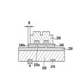
도 2는 본 발명의 바람직한 일 실시예에 따른 자기 센서를 나타낸 단면도.
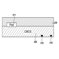
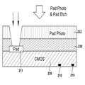
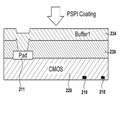
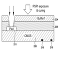
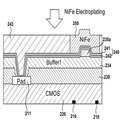
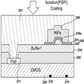
도 3a 내지 3p는 본 발명의 바람직한 일 실시예에 따른 반도체 기반의 자기 센서의 제조 방법을 설명하기 위한 단면도.
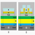
도 4는 종래의 평판형 자기 센서(A)와 본 발명의 일 실시예에 따른 자기 센서(B)의 단면 구조를 비교하여 나타낸 도면.
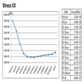
도 5a는 도 4의 자기 센서들의 홀소자에 미치는 X축 방향의 스트레스를 나타낸 그래프.
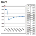
도 5b는 도 4의 자기 센서들의 홀소자에 미치는 Y축 방향의 스트레스를 나타낸 그래프.
도 6은 본 발명의 기초층의 돌출 길이에 따른 자기 센서의 단면 구조를 더욱 많은 실시예로 비교하여 나타낸 도면.
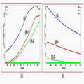
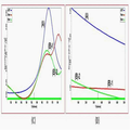
도 7은 도 6의 실시예들의 자기 센서들이 홀소자에 미치는 X축 및 Y축 방향의 스트레스를 나타낸 그래프.
도 8은 본 발명의 기초층의 돌출 길이에 따른 X축 방향의 스트레스 변화를 나타낸 그래프.
도 9는 본 발명의 기초층의 돌출 길이에 따른 Y축 방향의 스트레스 변화를 나타낸 그래프.
230 : 보호층 234 : 제1 버퍼층
235 : 예비 버퍼층 235a : 제2 버퍼층
240 : 기초층 250 : 자기 수속판
260 : 포토 레지스트
Claims (21)
- 복수의 홀소자가 배치된 반도체 기판;
상기 기판상에 형성된 보호층;
상기 보호층 상에 형성된 기초층; 및
상기 기초층 상에 형성되고, 그 표면상에 굴곡면을 갖는 자기 수속판을 구비하되,
상기 기초층의 면적은 상기 자기 수속판의 면적보다 넓은 것을 특징으로 하는 반도체 기반의 자기 센서. - 제 1항에 있어서,
상기 기초층의 테두리에는 상기 자기 수속판 외주면보다 일정 길이만큼 돌출된 돌출부가 형성된 것을 특징으로 하는 반도체 기반의 자기 센서. - 제 2항에 있어서,
상기 돌출부의 길이는 10 - 50㎛인 것을 특징으로 하는 반도체 기반의 자기 센서. - 제 1항에 있어서,
상기 보호층의 표면상에 제1 버퍼층과 복수의 일정한 높이를 가진 제2 버퍼층이 형성되고, 상기 기초층 및 자기 수속판은 상기 일정한 높이를 가진 제2 버퍼층의 형상에 따라 복수의 굴곡면이 형성되는 것을 특징으로 하는 반도체 기반의 자기 센서. - 제 4항에 있어서,
상기 일정한 높이를 가진 제2 버퍼층은 폴리이미드를 포함하는 것을 특징으로 하는 반도체 기반의 자기 센서. - 제 1항에 있어서,
상기 자기 수속판의 굴곡면은,
그 단면 형상이 다수의 요철(凹凸) 모양으로 규칙 또는 불규칙적으로 배열된 것을 특징으로 하는 반도체 기반의 자기 센서. - 제 1항에 있어서,
상기 복수의 홀소자는,
상기 자기 수속판의 끝단부와 일정 영역이 중첩되도록 배치되는 것을 특징으로 하는 반도체 기반의 자기 센서. - 제 1항에 있어서,
상기 기초층은 티타늄 또는 티타늄-텅스텐을 증착하고, 구리금속을 적층한 물질로 이루어진 것을 특징으로 하는 반도체 기반의 자기 센서. - 제 1항의 반도체 기반의 자기센서를 사용하여 제조된 것을 특징으로 하는 디지털 나침반.
- 복수의 홀소자가 설치된 기판을 형성하는 단계;
상기 기판상에 보호층을 형성하는 단계;
상기 보호층 상에 제1 버퍼층을 형성하는 단계;
상기 제1 버퍼층의 표면상에 복수의 일정한 높이를 가진 제2 버퍼층을 형성하는 단계;
상기 복수의 일정한 높이를 가진 제2 버퍼층에 대응되는 굴곡면을 갖는 기초층을 형성하는 단계; 및
상기 기초층 상에 굴곡면을 갖는 자기 수속판을 형성하되, 상기 기초층의 면적을 상기 자기 수속판의 면적보다 넓게 형성하는 단계;를 포함하는 것을 특징으로 하는 반도체 기반의 자기 센서의 제조 방법. - 제 10항에 있어서,
상기 자기 수속판 상부에 포토 공정을 통하여 상기 자기 수속판보다 큰 포토레지스트(PR)를 형성하고, 습식식각(wet etch)을 통해 상기 기초층을 제거함으로써, 상기 기초층의 테두리에 상기 자기 수속판 외주면보다 일정 길이만큼 돌출된 돌출부가 형성되도록 하는 것을 특징으로 하는 반도체 기반의 자기 센서의 제조 방법. - 제 11항에 있어서,
상기 돌출부의 길이는 10 - 50 ㎛ 인 것을 특징으로 하는 반도체 기반의 자기 센서의 제조 방법. - 제 10항에 있어서,
상기 기초층 및 자기 수속판은 상기 제2 버퍼층의 형상에 따라 복수의 굴곡면이 형성되는 것을 특징으로 하는 반도체 기반의 자기 센서의 제조 방법. - 제 13항에 있어서,
상기 제2 버퍼층은 폴리이미드를 포함하는 것을 특징으로 하는 반도체 기반의 자기 센서의 제조 방법. - 제 10항에 있어서,
상기 기초층 및 자기 수속판의 굴곡면은,
그 단면 형상이 다수의 요철(凹凸) 모양으로 규칙 또는 불규칙적으로 배열된 것을 특징으로 하는 반도체 기반의 자기 센서의 제조 방법. - 제 10항에 있어서,
상기 복수의 홀소자는,
상기 자기 수속판의 끝단부와 일정 영역이 중첩되도록 배치되는 것을 특징으로 하는 반도체 기반의 자기 센서의 제조 방법. - 제 10항에 있어서,
상기 기초층은 티타늄 또는 티타늄-텅스텐을 증착하고, 구리금속을 적층한 물질로 이루어진 것을 특징으로 하는 반도체 기반의 자기 센서의 제조 방법. - 홀소자가 배치된 반도체 기판;
상기 기판상에 형성된 보호층;
상기 보호층 상에 형성된 기초층; 및
상기 기초층 상에 형성되고, 그 표면상에 굴곡면을 갖는 자기 수속판을 구비하되,
상기 기초층은 상기 홀소자의 끝단부보다 더 돌출된 것을 특징으로 하는 반도체 기반의 자기 센서. - 제 18항에 있어서,
상기 홀소자는 상기 기판에 N형 이온 주입 영역과 P형 이온 주입 영역으로 이루어진 것을 특징으로 하는 반도체 기반의 자기 센서. - 제 19항에 있어서,
상기 N형 이온 주입 영역은 상기 P형 이온 주입 영역보다 깊게 형성된 것을 특징으로 하는 반도체 기반의 자기 센서. - 제 18항에 있어서,
상기 홀소자는,
상기 자기 수속판의 끝단부와 일정 영역이 중첩되도록 배치되는 것을 특징으로 하는 반도체 기반의 자기 센서.
Priority Applications (4)
| Application Number | Priority Date | Filing Date | Title |
|---|---|---|---|
| KR1020130066892A KR101768254B1 (ko) | 2013-06-12 | 2013-06-12 | 반도체 기반의 자기 센서 및 그 제조 방법 |
| US13/963,174 US9018028B2 (en) | 2013-06-12 | 2013-08-09 | Magnetic sensor and method of manufacture thereof |
| EP13180539.2A EP2814065B1 (en) | 2013-06-12 | 2013-08-15 | Magnetic sensor and method of manufacture thereof |
| CN201310388598.1A CN104237812B (zh) | 2013-06-12 | 2013-08-30 | 磁传感器及其制造方法 |
Applications Claiming Priority (1)
| Application Number | Priority Date | Filing Date | Title |
|---|---|---|---|
| KR1020130066892A KR101768254B1 (ko) | 2013-06-12 | 2013-06-12 | 반도체 기반의 자기 센서 및 그 제조 방법 |
Publications (2)
| Publication Number | Publication Date |
|---|---|
| KR20140145227A true KR20140145227A (ko) | 2014-12-23 |
| KR101768254B1 KR101768254B1 (ko) | 2017-08-16 |
Family
ID=49000325
Family Applications (1)
| Application Number | Title | Priority Date | Filing Date |
|---|---|---|---|
| KR1020130066892A Active KR101768254B1 (ko) | 2013-06-12 | 2013-06-12 | 반도체 기반의 자기 센서 및 그 제조 방법 |
Country Status (4)
| Country | Link |
|---|---|
| US (1) | US9018028B2 (ko) |
| EP (1) | EP2814065B1 (ko) |
| KR (1) | KR101768254B1 (ko) |
| CN (1) | CN104237812B (ko) |
Cited By (4)
| Publication number | Priority date | Publication date | Assignee | Title |
|---|---|---|---|---|
| KR20170092300A (ko) | 2016-02-03 | 2017-08-11 | 고려대학교 세종산학협력단 | 스핀홀 현상을 이용한 자기장 측정 장치 및 방법 |
| KR20170107379A (ko) * | 2016-03-15 | 2017-09-25 | 에스아이아이 세미컨덕터 가부시키가이샤 | 자기 센서 및 그것의 제조 방법 |
| KR20170107402A (ko) * | 2016-03-15 | 2017-09-25 | 에스아이아이 세미컨덕터 가부시키가이샤 | 자기 센서 및 그 제조 방법 |
| KR20170107403A (ko) * | 2016-03-15 | 2017-09-25 | 에스아이아이 세미컨덕터 가부시키가이샤 | 반도체 장치와 그것의 제조 방법 |
Families Citing this family (19)
| Publication number | Priority date | Publication date | Assignee | Title |
|---|---|---|---|---|
| KR102116147B1 (ko) | 2014-03-06 | 2020-05-28 | 매그나칩 반도체 유한회사 | 매립형 마그네틱 센서 |
| US9741924B2 (en) * | 2015-02-26 | 2017-08-22 | Sii Semiconductor Corporation | Magnetic sensor having a recessed die pad |
| JP6604730B2 (ja) * | 2015-03-17 | 2019-11-13 | エイブリック株式会社 | 半導体装置 |
| JP6663259B2 (ja) * | 2016-03-15 | 2020-03-11 | エイブリック株式会社 | 半導体装置とその製造方法 |
| EP3276365B1 (en) * | 2016-07-26 | 2020-02-12 | Melexis Technologies SA | A sensor device with a soft magnetic alloy having reduced coercivity, and method for making same |
| US10760981B2 (en) * | 2016-11-18 | 2020-09-01 | Asahi Kasei Microdevices Corporation | Hall sensor |
| WO2019111782A1 (ja) * | 2017-12-04 | 2019-06-13 | 株式会社村田製作所 | 磁気センサ |
| EP3675172B8 (en) * | 2018-12-24 | 2023-10-18 | Crocus Technology Sa | Magnetic reader sensor device for reading magnetic stripes and method for manufacturing the sensor device |
| EP4224186B1 (en) * | 2019-05-24 | 2024-10-16 | Melexis Technologies SA | Semiconductor device with embedded magnetic flux concentrator |
| US11237223B2 (en) * | 2019-07-24 | 2022-02-01 | Texas Instruments Incorporated | Magnetic flux concentrator for in-plane direction magnetic field concentration |
| US20210072327A1 (en) * | 2019-09-09 | 2021-03-11 | Texas Instruments Incorporated | Magnetic flux concentrator for out-of-plane direction magnetic field concentration |
| CN111341217B (zh) * | 2020-02-21 | 2021-10-08 | 武汉华星光电半导体显示技术有限公司 | 显示面板及显示装置 |
| US11830833B2 (en) * | 2020-07-24 | 2023-11-28 | Innolux Corporation | Electronic substrate and electronic device |
| JPWO2022107763A1 (ko) | 2020-11-23 | 2022-05-27 | ||
| JP7759626B2 (ja) | 2020-11-23 | 2025-10-24 | パナソニックIpマネジメント株式会社 | 磁気センサ |
| JPWO2022107764A1 (ko) * | 2020-11-23 | 2022-05-27 | ||
| JP2021071488A (ja) * | 2021-01-05 | 2021-05-06 | エイブリック株式会社 | 磁気センサ |
| WO2023162584A1 (ja) * | 2022-02-24 | 2023-08-31 | 株式会社村田製作所 | 磁気センサ |
| CN119255694B (zh) * | 2024-12-04 | 2025-03-18 | 苏州矩阵光电有限公司 | 水平方向检测的霍尔集成芯片 |
Family Cites Families (15)
| Publication number | Priority date | Publication date | Assignee | Title |
|---|---|---|---|---|
| DE3590792C2 (ko) * | 1985-05-10 | 1991-05-23 | Asahi Kasei Kogyo K.K., Osaka, Jp | |
| JP3494921B2 (ja) * | 1999-05-31 | 2004-02-09 | 矢崎総業株式会社 | 磁電変換素子及びその製造方法 |
| JP2000349363A (ja) * | 1999-06-07 | 2000-12-15 | Yazaki Corp | 磁電変換素子及びその製造方法 |
| JP4936299B2 (ja) | 2000-08-21 | 2012-05-23 | メレクシス・テクノロジーズ・ナムローゼフェンノートシャップ | 磁場方向検出センサ |
| JP2003294818A (ja) * | 2002-03-28 | 2003-10-15 | Asahi Kasei Corp | 磁気センサおよびその製造方法 |
| JP2004271244A (ja) * | 2003-03-05 | 2004-09-30 | Asahi Kasei Electronics Co Ltd | 磁気センサ |
| JP2005333103A (ja) * | 2004-03-30 | 2005-12-02 | Denso Corp | 縦型ホール素子およびその製造方法 |
| US7358724B2 (en) * | 2005-05-16 | 2008-04-15 | Allegro Microsystems, Inc. | Integrated magnetic flux concentrator |
| JP4994365B2 (ja) * | 2006-04-03 | 2012-08-08 | 旭化成エレクトロニクス株式会社 | ホール素子及び磁気センサ |
| EP2960667A1 (en) * | 2006-04-13 | 2015-12-30 | Asahi Kasei EMD Corporation | Magnetic sensor and method for fabricating the same |
| JP4903543B2 (ja) * | 2006-05-18 | 2012-03-28 | 旭化成エレクトロニクス株式会社 | 磁気センサ及びその製造方法 |
| JP5064732B2 (ja) * | 2006-07-12 | 2012-10-31 | 旭化成エレクトロニクス株式会社 | 磁気センサ及びその製造方法 |
| JP4792143B2 (ja) * | 2007-02-22 | 2011-10-12 | 株式会社デンソー | 半導体装置およびその製造方法 |
| CN103257325A (zh) * | 2007-03-23 | 2013-08-21 | 旭化成微电子株式会社 | 磁传感器及其灵敏度测量方法 |
| KR101876587B1 (ko) * | 2013-03-08 | 2018-08-03 | 매그나칩 반도체 유한회사 | 자기 센서 및 그 제조 방법 |
-
2013
- 2013-06-12 KR KR1020130066892A patent/KR101768254B1/ko active Active
- 2013-08-09 US US13/963,174 patent/US9018028B2/en active Active
- 2013-08-15 EP EP13180539.2A patent/EP2814065B1/en active Active
- 2013-08-30 CN CN201310388598.1A patent/CN104237812B/zh active Active
Cited By (4)
| Publication number | Priority date | Publication date | Assignee | Title |
|---|---|---|---|---|
| KR20170092300A (ko) | 2016-02-03 | 2017-08-11 | 고려대학교 세종산학협력단 | 스핀홀 현상을 이용한 자기장 측정 장치 및 방법 |
| KR20170107379A (ko) * | 2016-03-15 | 2017-09-25 | 에스아이아이 세미컨덕터 가부시키가이샤 | 자기 센서 및 그것의 제조 방법 |
| KR20170107402A (ko) * | 2016-03-15 | 2017-09-25 | 에스아이아이 세미컨덕터 가부시키가이샤 | 자기 센서 및 그 제조 방법 |
| KR20170107403A (ko) * | 2016-03-15 | 2017-09-25 | 에스아이아이 세미컨덕터 가부시키가이샤 | 반도체 장치와 그것의 제조 방법 |
Also Published As
| Publication number | Publication date |
|---|---|
| CN104237812A (zh) | 2014-12-24 |
| US20140367813A1 (en) | 2014-12-18 |
| US9018028B2 (en) | 2015-04-28 |
| CN104237812B (zh) | 2018-01-09 |
| EP2814065B1 (en) | 2017-04-12 |
| KR101768254B1 (ko) | 2017-08-16 |
| EP2814065A3 (en) | 2015-11-11 |
| EP2814065A2 (en) | 2014-12-17 |
Similar Documents
| Publication | Publication Date | Title |
|---|---|---|
| KR101768254B1 (ko) | 반도체 기반의 자기 센서 및 그 제조 방법 | |
| US10256396B2 (en) | Magnetic sensor and method of fabricating the same | |
| US20160258824A1 (en) | Strain sensing element, pressure sensor, and microphone | |
| KR20080111469A (ko) | 자기 센서 및 그 제조 방법 | |
| WO2015144073A1 (zh) | 一种单芯片三轴磁场传感器及其制备方法 | |
| US20140159717A1 (en) | Magnetoresistive sensor integrated in a chip for detecting magnetic fields perpendicular to the chip and manufacturing process thereof | |
| US10727402B2 (en) | Method for producing tunnel magnetoresistive element | |
| CN114442011B (zh) | 磁传感器设备 | |
| CN107526046B (zh) | 一种平面电感型磁传感器 | |
| CN204964732U (zh) | 单芯片三轴各向异性磁阻传感器 | |
| CN105304811B (zh) | 具有斜面的衬底结构、磁阻传感器及其制作方法 | |
| US9523747B2 (en) | Magnetoresistive device and method for manufacturing the same | |
| JP4903543B2 (ja) | 磁気センサ及びその製造方法 | |
| US9513346B2 (en) | Magnetic sensors with permanent magnets magnetized in different directions | |
| US9625536B2 (en) | Magnetic sensor and method for manufacturing the same | |
| CN112289925B (zh) | 磁传感器的制备方法 | |
| CN104597417B (zh) | 具有带有永久磁体的磁传感器的装置 | |
| CN107819034B (zh) | 晶体管及其制造方法 | |
| JP2007108011A (ja) | 磁気センサ及びその製造方法 | |
| US10563306B2 (en) | Production method for a layer structure and layer structure | |
| CN118678869A (zh) | 一种基于磁隧道结的芯片结构及芯片结构的制作方法 | |
| CN104483637A (zh) | 提高第三轴感应能力的磁传感器及其制备工艺 | |
| TW201530174A (zh) | 具有永久磁力之磁感測器之裝置 |
Legal Events
| Date | Code | Title | Description |
|---|---|---|---|
| PA0109 | Patent application |
Patent event code: PA01091R01D Comment text: Patent Application Patent event date: 20130612 |
|
| PG1501 | Laying open of application | ||
| A201 | Request for examination | ||
| PA0201 | Request for examination |
Patent event code: PA02012R01D Patent event date: 20160421 Comment text: Request for Examination of Application Patent event code: PA02011R01I Patent event date: 20130612 Comment text: Patent Application |
|
| E902 | Notification of reason for refusal | ||
| PE0902 | Notice of grounds for rejection |
Comment text: Notification of reason for refusal Patent event date: 20170308 Patent event code: PE09021S01D |
|
| E701 | Decision to grant or registration of patent right | ||
| PE0701 | Decision of registration |
Patent event code: PE07011S01D Comment text: Decision to Grant Registration Patent event date: 20170802 |
|
| GRNT | Written decision to grant | ||
| PR0701 | Registration of establishment |
Comment text: Registration of Establishment Patent event date: 20170808 Patent event code: PR07011E01D |
|
| PR1002 | Payment of registration fee |
Payment date: 20170808 End annual number: 3 Start annual number: 1 |
|
| PG1601 | Publication of registration | ||
| PR1001 | Payment of annual fee |
Payment date: 20200716 Start annual number: 4 End annual number: 4 |
|
| PR1001 | Payment of annual fee |
Payment date: 20210802 Start annual number: 5 End annual number: 5 |
|
| PR1001 | Payment of annual fee |
Payment date: 20220721 Start annual number: 6 End annual number: 6 |
|
| PR1001 | Payment of annual fee |
Payment date: 20230801 Start annual number: 7 End annual number: 7 |