KR20160032009A - 감광성 수지 조성물, 필름상 접착제, 접착 시트, 접착제 패턴, 접착제층이 형성된 반도체 웨이퍼 및 반도체 장치 - Google Patents
감광성 수지 조성물, 필름상 접착제, 접착 시트, 접착제 패턴, 접착제층이 형성된 반도체 웨이퍼 및 반도체 장치 Download PDFInfo
- Publication number
- KR20160032009A KR20160032009A KR1020157034602A KR20157034602A KR20160032009A KR 20160032009 A KR20160032009 A KR 20160032009A KR 1020157034602 A KR1020157034602 A KR 1020157034602A KR 20157034602 A KR20157034602 A KR 20157034602A KR 20160032009 A KR20160032009 A KR 20160032009A
- Authority
- KR
- South Korea
- Prior art keywords
- adhesive
- group
- film
- resin composition
- mass
- Prior art date
- Legal status (The legal status is an assumption and is not a legal conclusion. Google has not performed a legal analysis and makes no representation as to the accuracy of the status listed.)
- Ceased
Links
- JEFSGXDPIHRGAV-UHFFFAOYSA-N CC(C=C1)=CCC1OC Chemical compound CC(C=C1)=CCC1OC JEFSGXDPIHRGAV-UHFFFAOYSA-N 0.000 description 1
- 0 CC1*CCCC1 Chemical compound CC1*CCCC1 0.000 description 1
- CHLICZRVGGXEOD-UHFFFAOYSA-N Cc(cc1)ccc1OC Chemical compound Cc(cc1)ccc1OC CHLICZRVGGXEOD-UHFFFAOYSA-N 0.000 description 1
Images







Classifications
-
- C—CHEMISTRY; METALLURGY
- C09—DYES; PAINTS; POLISHES; NATURAL RESINS; ADHESIVES; COMPOSITIONS NOT OTHERWISE PROVIDED FOR; APPLICATIONS OF MATERIALS NOT OTHERWISE PROVIDED FOR
- C09J—ADHESIVES; NON-MECHANICAL ASPECTS OF ADHESIVE PROCESSES IN GENERAL; ADHESIVE PROCESSES NOT PROVIDED FOR ELSEWHERE; USE OF MATERIALS AS ADHESIVES
- C09J179/00—Adhesives based on macromolecular compounds obtained by reactions forming in the main chain of the macromolecule a linkage containing nitrogen, with or without oxygen, or carbon only, not provided for in groups C09J161/00 - C09J177/00
- C09J179/04—Polycondensates having nitrogen-containing heterocyclic rings in the main chain; Polyhydrazides; Polyamide acids or similar polyimide precursors
- C09J179/08—Polyimides; Polyester-imides; Polyamide-imides; Polyamide acids or similar polyimide precursors
-
- C09J7/02—
-
- C—CHEMISTRY; METALLURGY
- C09—DYES; PAINTS; POLISHES; NATURAL RESINS; ADHESIVES; COMPOSITIONS NOT OTHERWISE PROVIDED FOR; APPLICATIONS OF MATERIALS NOT OTHERWISE PROVIDED FOR
- C09J—ADHESIVES; NON-MECHANICAL ASPECTS OF ADHESIVE PROCESSES IN GENERAL; ADHESIVE PROCESSES NOT PROVIDED FOR ELSEWHERE; USE OF MATERIALS AS ADHESIVES
- C09J7/00—Adhesives in the form of films or foils
- C09J7/20—Adhesives in the form of films or foils characterised by their carriers
-
- G—PHYSICS
- G03—PHOTOGRAPHY; CINEMATOGRAPHY; ANALOGOUS TECHNIQUES USING WAVES OTHER THAN OPTICAL WAVES; ELECTROGRAPHY; HOLOGRAPHY
- G03F—PHOTOMECHANICAL PRODUCTION OF TEXTURED OR PATTERNED SURFACES, e.g. FOR PRINTING, FOR PROCESSING OF SEMICONDUCTOR DEVICES; MATERIALS THEREFOR; ORIGINALS THEREFOR; APPARATUS SPECIALLY ADAPTED THEREFOR
- G03F7/00—Photomechanical, e.g. photolithographic, production of textured or patterned surfaces, e.g. printing surfaces; Materials therefor, e.g. comprising photoresists; Apparatus specially adapted therefor
- G03F7/004—Photosensitive materials
-
- G—PHYSICS
- G03—PHOTOGRAPHY; CINEMATOGRAPHY; ANALOGOUS TECHNIQUES USING WAVES OTHER THAN OPTICAL WAVES; ELECTROGRAPHY; HOLOGRAPHY
- G03F—PHOTOMECHANICAL PRODUCTION OF TEXTURED OR PATTERNED SURFACES, e.g. FOR PRINTING, FOR PROCESSING OF SEMICONDUCTOR DEVICES; MATERIALS THEREFOR; ORIGINALS THEREFOR; APPARATUS SPECIALLY ADAPTED THEREFOR
- G03F7/00—Photomechanical, e.g. photolithographic, production of textured or patterned surfaces, e.g. printing surfaces; Materials therefor, e.g. comprising photoresists; Apparatus specially adapted therefor
- G03F7/004—Photosensitive materials
- G03F7/027—Non-macromolecular photopolymerisable compounds having carbon-to-carbon double bonds, e.g. ethylenic compounds
-
- G—PHYSICS
- G03—PHOTOGRAPHY; CINEMATOGRAPHY; ANALOGOUS TECHNIQUES USING WAVES OTHER THAN OPTICAL WAVES; ELECTROGRAPHY; HOLOGRAPHY
- G03F—PHOTOMECHANICAL PRODUCTION OF TEXTURED OR PATTERNED SURFACES, e.g. FOR PRINTING, FOR PROCESSING OF SEMICONDUCTOR DEVICES; MATERIALS THEREFOR; ORIGINALS THEREFOR; APPARATUS SPECIALLY ADAPTED THEREFOR
- G03F7/00—Photomechanical, e.g. photolithographic, production of textured or patterned surfaces, e.g. printing surfaces; Materials therefor, e.g. comprising photoresists; Apparatus specially adapted therefor
- G03F7/004—Photosensitive materials
- G03F7/027—Non-macromolecular photopolymerisable compounds having carbon-to-carbon double bonds, e.g. ethylenic compounds
- G03F7/032—Non-macromolecular photopolymerisable compounds having carbon-to-carbon double bonds, e.g. ethylenic compounds with binders
- G03F7/037—Non-macromolecular photopolymerisable compounds having carbon-to-carbon double bonds, e.g. ethylenic compounds with binders the binders being polyamides or polyimides
-
- G—PHYSICS
- G03—PHOTOGRAPHY; CINEMATOGRAPHY; ANALOGOUS TECHNIQUES USING WAVES OTHER THAN OPTICAL WAVES; ELECTROGRAPHY; HOLOGRAPHY
- G03F—PHOTOMECHANICAL PRODUCTION OF TEXTURED OR PATTERNED SURFACES, e.g. FOR PRINTING, FOR PROCESSING OF SEMICONDUCTOR DEVICES; MATERIALS THEREFOR; ORIGINALS THEREFOR; APPARATUS SPECIALLY ADAPTED THEREFOR
- G03F7/00—Photomechanical, e.g. photolithographic, production of textured or patterned surfaces, e.g. printing surfaces; Materials therefor, e.g. comprising photoresists; Apparatus specially adapted therefor
- G03F7/004—Photosensitive materials
- G03F7/038—Macromolecular compounds which are rendered insoluble or differentially wettable
-
- G—PHYSICS
- G03—PHOTOGRAPHY; CINEMATOGRAPHY; ANALOGOUS TECHNIQUES USING WAVES OTHER THAN OPTICAL WAVES; ELECTROGRAPHY; HOLOGRAPHY
- G03F—PHOTOMECHANICAL PRODUCTION OF TEXTURED OR PATTERNED SURFACES, e.g. FOR PRINTING, FOR PROCESSING OF SEMICONDUCTOR DEVICES; MATERIALS THEREFOR; ORIGINALS THEREFOR; APPARATUS SPECIALLY ADAPTED THEREFOR
- G03F7/00—Photomechanical, e.g. photolithographic, production of textured or patterned surfaces, e.g. printing surfaces; Materials therefor, e.g. comprising photoresists; Apparatus specially adapted therefor
- G03F7/004—Photosensitive materials
- G03F7/038—Macromolecular compounds which are rendered insoluble or differentially wettable
- G03F7/0387—Polyamides or polyimides
-
- G—PHYSICS
- G03—PHOTOGRAPHY; CINEMATOGRAPHY; ANALOGOUS TECHNIQUES USING WAVES OTHER THAN OPTICAL WAVES; ELECTROGRAPHY; HOLOGRAPHY
- G03F—PHOTOMECHANICAL PRODUCTION OF TEXTURED OR PATTERNED SURFACES, e.g. FOR PRINTING, FOR PROCESSING OF SEMICONDUCTOR DEVICES; MATERIALS THEREFOR; ORIGINALS THEREFOR; APPARATUS SPECIALLY ADAPTED THEREFOR
- G03F7/00—Photomechanical, e.g. photolithographic, production of textured or patterned surfaces, e.g. printing surfaces; Materials therefor, e.g. comprising photoresists; Apparatus specially adapted therefor
- G03F7/004—Photosensitive materials
- G03F7/075—Silicon-containing compounds
- G03F7/0751—Silicon-containing compounds used as adhesion-promoting additives or as means to improve adhesion
-
- H01L21/02304—
-
- H01L21/185—
-
- C—CHEMISTRY; METALLURGY
- C09—DYES; PAINTS; POLISHES; NATURAL RESINS; ADHESIVES; COMPOSITIONS NOT OTHERWISE PROVIDED FOR; APPLICATIONS OF MATERIALS NOT OTHERWISE PROVIDED FOR
- C09J—ADHESIVES; NON-MECHANICAL ASPECTS OF ADHESIVE PROCESSES IN GENERAL; ADHESIVE PROCESSES NOT PROVIDED FOR ELSEWHERE; USE OF MATERIALS AS ADHESIVES
- C09J2203/00—Applications of adhesives in processes or use of adhesives in the form of films or foils
- C09J2203/326—Applications of adhesives in processes or use of adhesives in the form of films or foils for bonding electronic components such as wafers, chips or semiconductors
-
- C—CHEMISTRY; METALLURGY
- C09—DYES; PAINTS; POLISHES; NATURAL RESINS; ADHESIVES; COMPOSITIONS NOT OTHERWISE PROVIDED FOR; APPLICATIONS OF MATERIALS NOT OTHERWISE PROVIDED FOR
- C09J—ADHESIVES; NON-MECHANICAL ASPECTS OF ADHESIVE PROCESSES IN GENERAL; ADHESIVE PROCESSES NOT PROVIDED FOR ELSEWHERE; USE OF MATERIALS AS ADHESIVES
- C09J2301/00—Additional features of adhesives in the form of films or foils
- C09J2301/10—Additional features of adhesives in the form of films or foils characterized by the structural features of the adhesive tape or sheet
- C09J2301/12—Additional features of adhesives in the form of films or foils characterized by the structural features of the adhesive tape or sheet by the arrangement of layers
- C09J2301/122—Additional features of adhesives in the form of films or foils characterized by the structural features of the adhesive tape or sheet by the arrangement of layers the adhesive layer being present only on one side of the carrier, e.g. single-sided adhesive tape
-
- C—CHEMISTRY; METALLURGY
- C09—DYES; PAINTS; POLISHES; NATURAL RESINS; ADHESIVES; COMPOSITIONS NOT OTHERWISE PROVIDED FOR; APPLICATIONS OF MATERIALS NOT OTHERWISE PROVIDED FOR
- C09J—ADHESIVES; NON-MECHANICAL ASPECTS OF ADHESIVE PROCESSES IN GENERAL; ADHESIVE PROCESSES NOT PROVIDED FOR ELSEWHERE; USE OF MATERIALS AS ADHESIVES
- C09J2301/00—Additional features of adhesives in the form of films or foils
- C09J2301/40—Additional features of adhesives in the form of films or foils characterized by the presence of essential components
- C09J2301/416—Additional features of adhesives in the form of films or foils characterized by the presence of essential components use of irradiation
-
- C—CHEMISTRY; METALLURGY
- C09—DYES; PAINTS; POLISHES; NATURAL RESINS; ADHESIVES; COMPOSITIONS NOT OTHERWISE PROVIDED FOR; APPLICATIONS OF MATERIALS NOT OTHERWISE PROVIDED FOR
- C09J—ADHESIVES; NON-MECHANICAL ASPECTS OF ADHESIVE PROCESSES IN GENERAL; ADHESIVE PROCESSES NOT PROVIDED FOR ELSEWHERE; USE OF MATERIALS AS ADHESIVES
- C09J2479/00—Presence of polyamine or polyimide
- C09J2479/08—Presence of polyamine or polyimide polyimide
-
- H—ELECTRICITY
- H10—SEMICONDUCTOR DEVICES; ELECTRIC SOLID-STATE DEVICES NOT OTHERWISE PROVIDED FOR
- H10W—GENERIC PACKAGES, INTERCONNECTIONS, CONNECTORS OR OTHER CONSTRUCTIONAL DETAILS OF DEVICES COVERED BY CLASS H10
- H10W72/00—Interconnections or connectors in packages
- H10W72/01—Manufacture or treatment
- H10W72/012—Manufacture or treatment of bump connectors, dummy bumps or thermal bumps
- H10W72/01221—Manufacture or treatment of bump connectors, dummy bumps or thermal bumps using local deposition
- H10W72/01223—Manufacture or treatment of bump connectors, dummy bumps or thermal bumps using local deposition in liquid form, e.g. by dispensing droplets or by screen printing
-
- H—ELECTRICITY
- H10—SEMICONDUCTOR DEVICES; ELECTRIC SOLID-STATE DEVICES NOT OTHERWISE PROVIDED FOR
- H10W—GENERIC PACKAGES, INTERCONNECTIONS, CONNECTORS OR OTHER CONSTRUCTIONAL DETAILS OF DEVICES COVERED BY CLASS H10
- H10W72/00—Interconnections or connectors in packages
- H10W72/01—Manufacture or treatment
- H10W72/012—Manufacture or treatment of bump connectors, dummy bumps or thermal bumps
- H10W72/01231—Manufacture or treatment of bump connectors, dummy bumps or thermal bumps using blanket deposition
- H10W72/01233—Manufacture or treatment of bump connectors, dummy bumps or thermal bumps using blanket deposition in liquid form, e.g. spin coating, spray coating or immersion coating
-
- H—ELECTRICITY
- H10—SEMICONDUCTOR DEVICES; ELECTRIC SOLID-STATE DEVICES NOT OTHERWISE PROVIDED FOR
- H10W—GENERIC PACKAGES, INTERCONNECTIONS, CONNECTORS OR OTHER CONSTRUCTIONAL DETAILS OF DEVICES COVERED BY CLASS H10
- H10W72/00—Interconnections or connectors in packages
- H10W72/01—Manufacture or treatment
- H10W72/012—Manufacture or treatment of bump connectors, dummy bumps or thermal bumps
- H10W72/01251—Changing the shapes of bumps
- H10W72/01255—Changing the shapes of bumps by using masks
-
- H—ELECTRICITY
- H10—SEMICONDUCTOR DEVICES; ELECTRIC SOLID-STATE DEVICES NOT OTHERWISE PROVIDED FOR
- H10W—GENERIC PACKAGES, INTERCONNECTIONS, CONNECTORS OR OTHER CONSTRUCTIONAL DETAILS OF DEVICES COVERED BY CLASS H10
- H10W72/00—Interconnections or connectors in packages
- H10W72/01—Manufacture or treatment
- H10W72/013—Manufacture or treatment of die-attach connectors
-
- H—ELECTRICITY
- H10—SEMICONDUCTOR DEVICES; ELECTRIC SOLID-STATE DEVICES NOT OTHERWISE PROVIDED FOR
- H10W—GENERIC PACKAGES, INTERCONNECTIONS, CONNECTORS OR OTHER CONSTRUCTIONAL DETAILS OF DEVICES COVERED BY CLASS H10
- H10W72/00—Interconnections or connectors in packages
- H10W72/01—Manufacture or treatment
- H10W72/013—Manufacture or treatment of die-attach connectors
- H10W72/01304—Manufacture or treatment of die-attach connectors using temporary auxiliary members, e.g. using sacrificial coatings or handle substrates
-
- H—ELECTRICITY
- H10—SEMICONDUCTOR DEVICES; ELECTRIC SOLID-STATE DEVICES NOT OTHERWISE PROVIDED FOR
- H10W—GENERIC PACKAGES, INTERCONNECTIONS, CONNECTORS OR OTHER CONSTRUCTIONAL DETAILS OF DEVICES COVERED BY CLASS H10
- H10W72/00—Interconnections or connectors in packages
- H10W72/01—Manufacture or treatment
- H10W72/013—Manufacture or treatment of die-attach connectors
- H10W72/01331—Manufacture or treatment of die-attach connectors using blanket deposition
- H10W72/01336—Manufacture or treatment of die-attach connectors using blanket deposition in solid form, e.g. by using a powder or by laminating a foil
-
- H—ELECTRICITY
- H10—SEMICONDUCTOR DEVICES; ELECTRIC SOLID-STATE DEVICES NOT OTHERWISE PROVIDED FOR
- H10W—GENERIC PACKAGES, INTERCONNECTIONS, CONNECTORS OR OTHER CONSTRUCTIONAL DETAILS OF DEVICES COVERED BY CLASS H10
- H10W72/00—Interconnections or connectors in packages
- H10W72/01—Manufacture or treatment
- H10W72/013—Manufacture or treatment of die-attach connectors
- H10W72/01351—Changing the shapes of die-attach connectors
-
- H—ELECTRICITY
- H10—SEMICONDUCTOR DEVICES; ELECTRIC SOLID-STATE DEVICES NOT OTHERWISE PROVIDED FOR
- H10W—GENERIC PACKAGES, INTERCONNECTIONS, CONNECTORS OR OTHER CONSTRUCTIONAL DETAILS OF DEVICES COVERED BY CLASS H10
- H10W72/00—Interconnections or connectors in packages
- H10W72/01—Manufacture or treatment
- H10W72/013—Manufacture or treatment of die-attach connectors
- H10W72/01361—Chemical or physical modification, e.g. by sintering or anodisation
-
- H—ELECTRICITY
- H10—SEMICONDUCTOR DEVICES; ELECTRIC SOLID-STATE DEVICES NOT OTHERWISE PROVIDED FOR
- H10W—GENERIC PACKAGES, INTERCONNECTIONS, CONNECTORS OR OTHER CONSTRUCTIONAL DETAILS OF DEVICES COVERED BY CLASS H10
- H10W72/00—Interconnections or connectors in packages
- H10W72/01—Manufacture or treatment
- H10W72/013—Manufacture or treatment of die-attach connectors
- H10W72/01365—Thermally treating
-
- H—ELECTRICITY
- H10—SEMICONDUCTOR DEVICES; ELECTRIC SOLID-STATE DEVICES NOT OTHERWISE PROVIDED FOR
- H10W—GENERIC PACKAGES, INTERCONNECTIONS, CONNECTORS OR OTHER CONSTRUCTIONAL DETAILS OF DEVICES COVERED BY CLASS H10
- H10W72/00—Interconnections or connectors in packages
- H10W72/01—Manufacture or treatment
- H10W72/0198—Manufacture or treatment batch processes
-
- H—ELECTRICITY
- H10—SEMICONDUCTOR DEVICES; ELECTRIC SOLID-STATE DEVICES NOT OTHERWISE PROVIDED FOR
- H10W—GENERIC PACKAGES, INTERCONNECTIONS, CONNECTORS OR OTHER CONSTRUCTIONAL DETAILS OF DEVICES COVERED BY CLASS H10
- H10W72/00—Interconnections or connectors in packages
- H10W72/071—Connecting or disconnecting
- H10W72/072—Connecting or disconnecting of bump connectors
- H10W72/07202—Connecting or disconnecting of bump connectors using auxiliary members
- H10W72/07204—Connecting or disconnecting of bump connectors using auxiliary members using temporary auxiliary members, e.g. sacrificial coatings
-
- H—ELECTRICITY
- H10—SEMICONDUCTOR DEVICES; ELECTRIC SOLID-STATE DEVICES NOT OTHERWISE PROVIDED FOR
- H10W—GENERIC PACKAGES, INTERCONNECTIONS, CONNECTORS OR OTHER CONSTRUCTIONAL DETAILS OF DEVICES COVERED BY CLASS H10
- H10W72/00—Interconnections or connectors in packages
- H10W72/071—Connecting or disconnecting
- H10W72/072—Connecting or disconnecting of bump connectors
- H10W72/07231—Techniques
- H10W72/07232—Compression bonding, e.g. thermocompression bonding
-
- H—ELECTRICITY
- H10—SEMICONDUCTOR DEVICES; ELECTRIC SOLID-STATE DEVICES NOT OTHERWISE PROVIDED FOR
- H10W—GENERIC PACKAGES, INTERCONNECTIONS, CONNECTORS OR OTHER CONSTRUCTIONAL DETAILS OF DEVICES COVERED BY CLASS H10
- H10W72/00—Interconnections or connectors in packages
- H10W72/071—Connecting or disconnecting
- H10W72/073—Connecting or disconnecting of die-attach connectors
- H10W72/07302—Connecting or disconnecting of die-attach connectors using an auxiliary member
- H10W72/07304—Connecting or disconnecting of die-attach connectors using an auxiliary member the auxiliary member being temporary, e.g. a sacrificial coating
-
- H—ELECTRICITY
- H10—SEMICONDUCTOR DEVICES; ELECTRIC SOLID-STATE DEVICES NOT OTHERWISE PROVIDED FOR
- H10W—GENERIC PACKAGES, INTERCONNECTIONS, CONNECTORS OR OTHER CONSTRUCTIONAL DETAILS OF DEVICES COVERED BY CLASS H10
- H10W72/00—Interconnections or connectors in packages
- H10W72/071—Connecting or disconnecting
- H10W72/073—Connecting or disconnecting of die-attach connectors
- H10W72/07331—Connecting techniques
- H10W72/07332—Compression bonding, e.g. thermocompression bonding
-
- H—ELECTRICITY
- H10—SEMICONDUCTOR DEVICES; ELECTRIC SOLID-STATE DEVICES NOT OTHERWISE PROVIDED FOR
- H10W—GENERIC PACKAGES, INTERCONNECTIONS, CONNECTORS OR OTHER CONSTRUCTIONAL DETAILS OF DEVICES COVERED BY CLASS H10
- H10W72/00—Interconnections or connectors in packages
- H10W72/071—Connecting or disconnecting
- H10W72/073—Connecting or disconnecting of die-attach connectors
- H10W72/07331—Connecting techniques
- H10W72/07337—Connecting techniques using a polymer adhesive, e.g. an adhesive based on silicone or epoxy
- H10W72/07338—Connecting techniques using a polymer adhesive, e.g. an adhesive based on silicone or epoxy hardening the adhesive by curing, e.g. thermosetting
-
- H—ELECTRICITY
- H10—SEMICONDUCTOR DEVICES; ELECTRIC SOLID-STATE DEVICES NOT OTHERWISE PROVIDED FOR
- H10W—GENERIC PACKAGES, INTERCONNECTIONS, CONNECTORS OR OTHER CONSTRUCTIONAL DETAILS OF DEVICES COVERED BY CLASS H10
- H10W72/00—Interconnections or connectors in packages
- H10W72/20—Bump connectors, e.g. solder bumps or copper pillars; Dummy bumps; Thermal bumps
- H10W72/221—Structures or relative sizes
- H10W72/225—Bumps having a filler embedded in a matrix
-
- H—ELECTRICITY
- H10—SEMICONDUCTOR DEVICES; ELECTRIC SOLID-STATE DEVICES NOT OTHERWISE PROVIDED FOR
- H10W—GENERIC PACKAGES, INTERCONNECTIONS, CONNECTORS OR OTHER CONSTRUCTIONAL DETAILS OF DEVICES COVERED BY CLASS H10
- H10W72/00—Interconnections or connectors in packages
- H10W72/20—Bump connectors, e.g. solder bumps or copper pillars; Dummy bumps; Thermal bumps
- H10W72/251—Materials
- H10W72/252—Materials comprising solid metals or solid metalloids, e.g. PbSn, Ag or Cu
-
- H—ELECTRICITY
- H10—SEMICONDUCTOR DEVICES; ELECTRIC SOLID-STATE DEVICES NOT OTHERWISE PROVIDED FOR
- H10W—GENERIC PACKAGES, INTERCONNECTIONS, CONNECTORS OR OTHER CONSTRUCTIONAL DETAILS OF DEVICES COVERED BY CLASS H10
- H10W72/00—Interconnections or connectors in packages
- H10W72/20—Bump connectors, e.g. solder bumps or copper pillars; Dummy bumps; Thermal bumps
- H10W72/251—Materials
- H10W72/253—Materials not comprising solid metals or solid metalloids, e.g. polymers or ceramics
-
- H—ELECTRICITY
- H10—SEMICONDUCTOR DEVICES; ELECTRIC SOLID-STATE DEVICES NOT OTHERWISE PROVIDED FOR
- H10W—GENERIC PACKAGES, INTERCONNECTIONS, CONNECTORS OR OTHER CONSTRUCTIONAL DETAILS OF DEVICES COVERED BY CLASS H10
- H10W72/00—Interconnections or connectors in packages
- H10W72/30—Die-attach connectors
- H10W72/321—Structures or relative sizes of die-attach connectors
- H10W72/325—Die-attach connectors having a filler embedded in a matrix
-
- H—ELECTRICITY
- H10—SEMICONDUCTOR DEVICES; ELECTRIC SOLID-STATE DEVICES NOT OTHERWISE PROVIDED FOR
- H10W—GENERIC PACKAGES, INTERCONNECTIONS, CONNECTORS OR OTHER CONSTRUCTIONAL DETAILS OF DEVICES COVERED BY CLASS H10
- H10W72/00—Interconnections or connectors in packages
- H10W72/30—Die-attach connectors
- H10W72/351—Materials of die-attach connectors
- H10W72/352—Materials of die-attach connectors comprising metals or metalloids, e.g. solders
-
- H—ELECTRICITY
- H10—SEMICONDUCTOR DEVICES; ELECTRIC SOLID-STATE DEVICES NOT OTHERWISE PROVIDED FOR
- H10W—GENERIC PACKAGES, INTERCONNECTIONS, CONNECTORS OR OTHER CONSTRUCTIONAL DETAILS OF DEVICES COVERED BY CLASS H10
- H10W72/00—Interconnections or connectors in packages
- H10W72/30—Die-attach connectors
- H10W72/351—Materials of die-attach connectors
- H10W72/353—Materials of die-attach connectors not comprising solid metals or solid metalloids, e.g. ceramics
-
- H—ELECTRICITY
- H10—SEMICONDUCTOR DEVICES; ELECTRIC SOLID-STATE DEVICES NOT OTHERWISE PROVIDED FOR
- H10W—GENERIC PACKAGES, INTERCONNECTIONS, CONNECTORS OR OTHER CONSTRUCTIONAL DETAILS OF DEVICES COVERED BY CLASS H10
- H10W72/00—Interconnections or connectors in packages
- H10W72/30—Die-attach connectors
- H10W72/351—Materials of die-attach connectors
- H10W72/353—Materials of die-attach connectors not comprising solid metals or solid metalloids, e.g. ceramics
- H10W72/354—Materials of die-attach connectors not comprising solid metals or solid metalloids, e.g. ceramics comprising polymers
-
- H—ELECTRICITY
- H10—SEMICONDUCTOR DEVICES; ELECTRIC SOLID-STATE DEVICES NOT OTHERWISE PROVIDED FOR
- H10W—GENERIC PACKAGES, INTERCONNECTIONS, CONNECTORS OR OTHER CONSTRUCTIONAL DETAILS OF DEVICES COVERED BY CLASS H10
- H10W74/00—Encapsulations, e.g. protective coatings
- H10W74/10—Encapsulations, e.g. protective coatings characterised by their shape or disposition
- H10W74/15—Encapsulations, e.g. protective coatings characterised by their shape or disposition on active surfaces of flip-chip devices, e.g. underfills
-
- H—ELECTRICITY
- H10—SEMICONDUCTOR DEVICES; ELECTRIC SOLID-STATE DEVICES NOT OTHERWISE PROVIDED FOR
- H10W—GENERIC PACKAGES, INTERCONNECTIONS, CONNECTORS OR OTHER CONSTRUCTIONAL DETAILS OF DEVICES COVERED BY CLASS H10
- H10W90/00—Package configurations
- H10W90/701—Package configurations characterised by the relative positions of pads or connectors relative to package parts
- H10W90/721—Package configurations characterised by the relative positions of pads or connectors relative to package parts of bump connectors
- H10W90/722—Package configurations characterised by the relative positions of pads or connectors relative to package parts of bump connectors between stacked chips
-
- H—ELECTRICITY
- H10—SEMICONDUCTOR DEVICES; ELECTRIC SOLID-STATE DEVICES NOT OTHERWISE PROVIDED FOR
- H10W—GENERIC PACKAGES, INTERCONNECTIONS, CONNECTORS OR OTHER CONSTRUCTIONAL DETAILS OF DEVICES COVERED BY CLASS H10
- H10W90/00—Package configurations
- H10W90/701—Package configurations characterised by the relative positions of pads or connectors relative to package parts
- H10W90/721—Package configurations characterised by the relative positions of pads or connectors relative to package parts of bump connectors
- H10W90/724—Package configurations characterised by the relative positions of pads or connectors relative to package parts of bump connectors between a chip and a stacked insulating package substrate, interposer or RDL
-
- H—ELECTRICITY
- H10—SEMICONDUCTOR DEVICES; ELECTRIC SOLID-STATE DEVICES NOT OTHERWISE PROVIDED FOR
- H10W—GENERIC PACKAGES, INTERCONNECTIONS, CONNECTORS OR OTHER CONSTRUCTIONAL DETAILS OF DEVICES COVERED BY CLASS H10
- H10W90/00—Package configurations
- H10W90/701—Package configurations characterised by the relative positions of pads or connectors relative to package parts
- H10W90/731—Package configurations characterised by the relative positions of pads or connectors relative to package parts of die-attach connectors
- H10W90/732—Package configurations characterised by the relative positions of pads or connectors relative to package parts of die-attach connectors between stacked chips
-
- H—ELECTRICITY
- H10—SEMICONDUCTOR DEVICES; ELECTRIC SOLID-STATE DEVICES NOT OTHERWISE PROVIDED FOR
- H10W—GENERIC PACKAGES, INTERCONNECTIONS, CONNECTORS OR OTHER CONSTRUCTIONAL DETAILS OF DEVICES COVERED BY CLASS H10
- H10W90/00—Package configurations
- H10W90/701—Package configurations characterised by the relative positions of pads or connectors relative to package parts
- H10W90/731—Package configurations characterised by the relative positions of pads or connectors relative to package parts of die-attach connectors
- H10W90/734—Package configurations characterised by the relative positions of pads or connectors relative to package parts of die-attach connectors between a chip and a stacked insulating package substrate, interposer or RDL
-
- H—ELECTRICITY
- H10—SEMICONDUCTOR DEVICES; ELECTRIC SOLID-STATE DEVICES NOT OTHERWISE PROVIDED FOR
- H10W—GENERIC PACKAGES, INTERCONNECTIONS, CONNECTORS OR OTHER CONSTRUCTIONAL DETAILS OF DEVICES COVERED BY CLASS H10
- H10W99/00—Subject matter not provided for in other groups of this subclass
Landscapes
- Physics & Mathematics (AREA)
- General Physics & Mathematics (AREA)
- Spectroscopy & Molecular Physics (AREA)
- Chemical & Material Sciences (AREA)
- Organic Chemistry (AREA)
- Chemical Kinetics & Catalysis (AREA)
- Adhesives Or Adhesive Processes (AREA)
- Materials For Photolithography (AREA)
- Adhesive Tapes (AREA)
- Engineering & Computer Science (AREA)
- Manufacturing & Machinery (AREA)
Abstract
Description

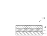
도 2는 본 발명의 접착 시트의 일실시형태를 나타낸 단면도이다.
도 3은 본 발명의 접착 시트의 일실시형태를 나타낸 단면도이다.
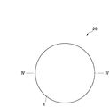
도 4는 본 발명의 접착제층이 형성된 반도체 웨이퍼의 일실시형태를 나타낸 상면도이다.
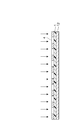
도 5는 도 4의 IV-IV선에 따른 단면도이다.
도 6은 본 발명의 반도체 장치의 일실시형태를 나타낸 단면도이다.
도 7은 본 발명의 반도체 장치의 제조 방법의 일실시형태를 나타낸 단면도이다.
도 8은 본 발명의 반도체 장치의 제조 방법의 일실시형태를 나타낸 단면도이다.
도 9는 본 발명의 반도체 장치의 제조 방법의 일실시형태를 나타낸 단면도이다.
도 10은 본 발명의 반도체 장치의 제조 방법의 일실시형태를 나타낸 단면도이다.
도 11은 본 발명의 반도체 장치의 제조 방법의 일실시형태를 나타낸 단면도이다.
도 12는 본 발명의 반도체 장치의 제조 방법의 일실시형태를 나타낸 단면도이다.








Claims (19)
- (A) 말단기로서 페놀성 수산기를 가지는 알칼리 가용성 수지;
(B) 방사선 중합성 화합물; 및
(C) 광 개시제
를 함유하는 감광성 수지 조성물. - 제1항에 있어서,
상기 알칼리 가용성 수지의 유리 전이 온도가 40℃∼150℃인, 감광성 수지 조성물. - 제1항 또는 제2항에 있어서,
상기 알칼리 가용성 수지가 말단기 및 측쇄기로서 페놀성 수산기를 가지는 폴리이미드 수지인, 감광성 수지 조성물. - 제1항 내지 제3항 중 어느 한 항에 있어서,
상기 알칼리 가용성 수지가,
테트라카르본산 이무수물;
페놀성 수산기 함유 디아민을 디아민 전체의 10 몰%∼80 몰% 함유하는 디아민; 및
페놀성 수산기 함유 아민
을 반응시켜 얻어지는 폴리이미드 수지인, 감광성 수지 조성물. - 제4항에 있어서,
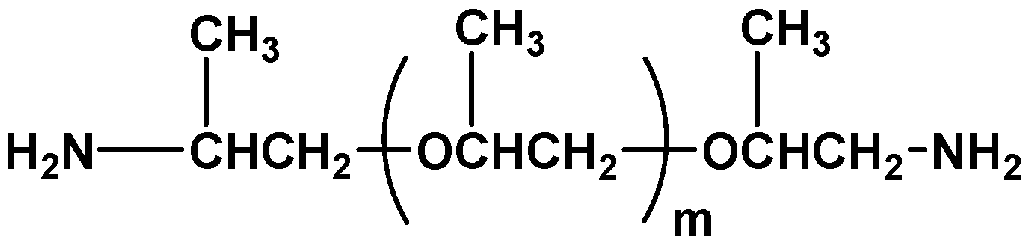
상기 디아민이, 하기 일반식(8)으로 표시되는 지방족 에테르 디아민을 디아민 전체의 10 몰%∼80 몰% 함유하는, 감광성 수지 조성물:

[상기 일반식(8) 중에서, R1∼R3는, 각각 독립적으로, 탄소수 1∼10의 알킬렌기를 나타내고, b는 2∼80의 정수를 나타냄]. - 제4항 또는 제5항에 있어서,
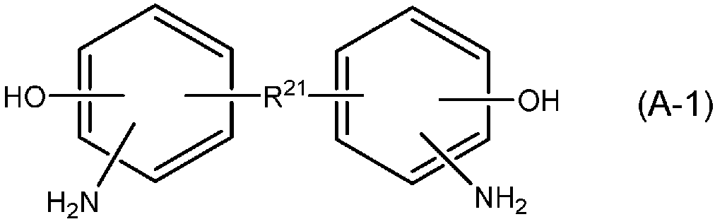
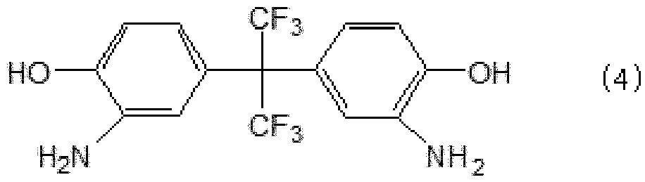
상기 페놀성 수산기 함유 디아민이, 하기 일반식(A-1)으로 표시되는 페놀성 수산기 함유 디아민을 포함하는, 감광성 수지 조성물:
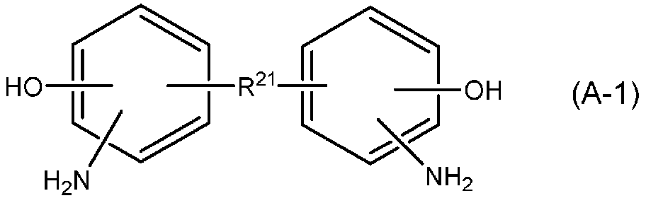
[상기 일반식(A-1) 중에서, R21은, 단결합 또는 2가의 유기기를 나타냄]. - 제1항 내지 제6항 중 어느 한 항에 있어서,
상기 알칼리 가용성 수지가, 알칼리 가용성기로서 페놀성 수산기만을 가지는 폴리이미드 수지인, 감광성 수지 조성물. - 제1항 내지 제7항 중 어느 한 항에 있어서,
상기 방사선 중합성 화합물이, 3관능 이상의 (메타)아크릴레이트를 적어도 1종 함유하는, 감광성 수지 조성물. - 제1항 내지 제8항 중 어느 한 항에 있어서,
(D) 에폭시 수지를 더 함유하는, 감광성 수지 조성물. - 제9항에 있어서,
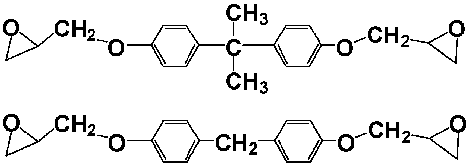
상기 에폭시 수지가, 비스페놀 F형 에폭시 수지 및 비스페놀 A형 에폭시 수지 중 적어도 1종을 함유하는, 감광성 수지 조성물. - 제1항 내지 제10항 중 어느 한 항에 있어서,
(E) 에틸렌성 불포화기 및 에폭시기를 가지는 화합물을 더 함유하는, 감광성 수지 조성물. - 제1항 내지 제11항 중 어느 한 항에 있어서,
(F) 필러(filler)를 더 함유하는, 감광성 수지 조성물. - 제1항 내지 제12항 중 어느 한 항에 있어서,
(G) 경화촉진제를 더 함유하는, 감광성 수지 조성물. - 제1항 내지 제13항 중 어느 한 항에 있어서,
반도체칩끼리의 접속 및/또는 반도체칩과 반도체칩 탑재용 지지 부재와의 접속에 사용되는 접착제용의, 감광성 수지 조성물. - 제1항 내지 제14항 중 어느 한 항에 기재된 감광성 수지 조성물을 필름상狀)으로 형성하는 것에 의해 얻어지는, 필름상 접착제.
- 기재(基材); 및
상기 기재 상에 형성된 제15항에 기재된 필름상 접착제로 이루어지는 접착제층
을 포함하는 접착 시트. - 피착체 상에 적층된 제15항에 기재된 필름상 접착제로 이루어지는 접착제층을 노광하고, 노광 후의 상기 접착제층을 알칼리 현상액으로 현상 처리함으로써 얻어지는, 접착제 패턴.
- 반도체 웨이퍼; 및
상기 반도체 웨이퍼 상에 적층된 제15항에 기재된 필름상 접착제로 이루어지는 접착제층
을 포함하는, 접착제층이 형성된 반도체 웨이퍼. - 제1항 내지 제14항 중 어느 한 항에 기재된 감광성 수지 조성물을 사용하여, 반도체칩끼리 접착된 구조, 및/또는 반도체칩과 반도체칩 탑재용 지지 부재가 접착된 구조를 가지는, 반도체 장치.
Applications Claiming Priority (1)
| Application Number | Priority Date | Filing Date | Title |
|---|---|---|---|
| PCT/JP2013/069303 WO2015008330A1 (ja) | 2013-07-16 | 2013-07-16 | 感光性樹脂組成物、フィルム状接着剤、接着シート、接着剤パターン、接着剤層付半導体ウェハ及び半導体装置 |
Publications (1)
| Publication Number | Publication Date |
|---|---|
| KR20160032009A true KR20160032009A (ko) | 2016-03-23 |
Family
ID=52345826
Family Applications (1)
| Application Number | Title | Priority Date | Filing Date |
|---|---|---|---|
| KR1020157034602A Ceased KR20160032009A (ko) | 2013-07-16 | 2013-07-16 | 감광성 수지 조성물, 필름상 접착제, 접착 시트, 접착제 패턴, 접착제층이 형성된 반도체 웨이퍼 및 반도체 장치 |
Country Status (4)
| Country | Link |
|---|---|
| US (1) | US10428253B2 (ko) |
| JP (1) | JP6436081B2 (ko) |
| KR (1) | KR20160032009A (ko) |
| WO (1) | WO2015008330A1 (ko) |
Families Citing this family (18)
| Publication number | Priority date | Publication date | Assignee | Title |
|---|---|---|---|---|
| US10155894B2 (en) * | 2014-07-07 | 2018-12-18 | Honeywell International Inc. | Thermal interface material with ion scavenger |
| CN107250317A (zh) | 2014-12-05 | 2017-10-13 | 霍尼韦尔国际公司 | 具有低热阻的高性能热界面材料 |
| US10474031B2 (en) * | 2015-03-27 | 2019-11-12 | Toray Industries, Inc. | Photosensitive resin composition, photosensitive resin composition film, cured product, insulating film and multilayer wiring board |
| EP3359603A1 (en) * | 2015-10-07 | 2018-08-15 | Henkel IP & Holding GmbH | Formulations and the use for 3d tsv packages |
| US10312177B2 (en) | 2015-11-17 | 2019-06-04 | Honeywell International Inc. | Thermal interface materials including a coloring agent |
| MX393621B (es) | 2016-03-08 | 2025-03-24 | Honeywell Int Inc | Material de camibo de fase. |
| JPWO2017169574A1 (ja) * | 2016-03-30 | 2019-02-14 | 東レ株式会社 | 感光性接着剤組成物、硬化物、感光性接着剤シート、積層基板および接着剤パターン付積層基板の製造方法 |
| US10501671B2 (en) | 2016-07-26 | 2019-12-10 | Honeywell International Inc. | Gel-type thermal interface material |
| TWI618979B (zh) * | 2017-06-30 | 2018-03-21 | 律勝科技股份有限公司 | 導熱型聚醯亞胺基板 |
| TWI618980B (zh) * | 2017-06-30 | 2018-03-21 | 律勝科技股份有限公司 | 導熱型感光性樹脂 |
| US11041103B2 (en) | 2017-09-08 | 2021-06-22 | Honeywell International Inc. | Silicone-free thermal gel |
| US10727195B2 (en) | 2017-09-15 | 2020-07-28 | Technetics Group Llc | Bond materials with enhanced plasma resistant characteristics and associated methods |
| US10428256B2 (en) | 2017-10-23 | 2019-10-01 | Honeywell International Inc. | Releasable thermal gel |
| US11072706B2 (en) | 2018-02-15 | 2021-07-27 | Honeywell International Inc. | Gel-type thermal interface material |
| JP7111031B2 (ja) * | 2018-03-23 | 2022-08-02 | 信越化学工業株式会社 | 感光性樹脂組成物、感光性樹脂積層体、及びパターン形成方法 |
| US11373921B2 (en) | 2019-04-23 | 2022-06-28 | Honeywell International Inc. | Gel-type thermal interface material with low pre-curing viscosity and elastic properties post-curing |
| KR102888782B1 (ko) | 2019-10-11 | 2025-11-24 | 삼성디스플레이 주식회사 | 접착 부재, 이를 포함한 표시장치, 및 표시장치의 제조 방법 |
| EP4498158A4 (en) * | 2022-03-22 | 2025-10-29 | Toray Industries | PHOTOSENSITIVE RESIN COMPOSITION, FILM BASED ON PHOTOSENSITIVE RESIN COMPOSITION, HARDENED PRODUCT AND ELECTRONIC COMPONENT USING IT |
Family Cites Families (55)
| Publication number | Priority date | Publication date | Assignee | Title |
|---|---|---|---|---|
| JP3999840B2 (ja) | 1997-04-16 | 2007-10-31 | 日東電工株式会社 | 封止用樹脂シート |
| JPH1124257A (ja) | 1997-07-04 | 1999-01-29 | Hitachi Chem Co Ltd | 感光性ポリイミド前駆体組成物及びそれを用いたパターン製造法 |
| JP2000290501A (ja) | 1999-04-05 | 2000-10-17 | Nitto Denko Corp | 感光性ポリイミド樹脂前駆体及び接着剤 |
| US6342333B1 (en) * | 1999-09-23 | 2002-01-29 | Hitachi Chemical Dupont Microsystems, L.L.C. | Photosensitive resin composition, patterning method, and electronic components |
| MY142246A (en) * | 2003-06-10 | 2010-11-15 | Hitachi Chemical Co Ltd | Adhesive film and process for preparing the same as well as adhesive sheet and semiconductor device |
| KR20070004100A (ko) * | 2004-04-20 | 2007-01-05 | 히다치 가세고교 가부시끼가이샤 | 접착시트, 반도체장치, 및 반도체장치의 제조방법 |
| JP4677758B2 (ja) * | 2004-10-14 | 2011-04-27 | 日立化成工業株式会社 | ダイボンドダイシングシート及びその製造方法、並びに、半導体装置の製造方法 |
| JP2006309202A (ja) | 2005-03-29 | 2006-11-09 | Toray Ind Inc | 感光性樹脂組成物およびそれを用いた半導体装置 |
| WO2006129630A1 (ja) * | 2005-05-31 | 2006-12-07 | Sumitomo Bakelite Co., Ltd. | プリアプライド用封止樹脂組成物、それを用いた半導体装置及びその製造方法 |
| JP5211438B2 (ja) * | 2005-06-09 | 2013-06-12 | 東レ株式会社 | 樹脂組成物およびそれを用いた表示装置 |
| EP1909142B1 (en) * | 2005-06-30 | 2015-06-24 | Toray Industries, Inc. | Photosensitive resin composition and adhesion enhancer |
| CN102290334B (zh) | 2005-07-05 | 2015-03-11 | 日立化成株式会社 | 半导体装置的制造方法 |
| JP2007180530A (ja) | 2005-12-01 | 2007-07-12 | Sumitomo Bakelite Co Ltd | 多層配線板および金属接合接着剤 |
| KR101014483B1 (ko) * | 2006-01-23 | 2011-02-14 | 히다치 가세고교 가부시끼가이샤 | 접착제 조성물, 필름상 접착제, 접착시트, 및 그것을이용한 반도체장치 |
| JP2008214549A (ja) | 2007-03-06 | 2008-09-18 | Sumitomo Bakelite Co Ltd | フェノール樹脂成形材料 |
| KR20100074296A (ko) * | 2007-12-04 | 2010-07-01 | 히다치 가세고교 가부시끼가이샤 | 감광성 접착제 |
| US20110121435A1 (en) | 2008-01-16 | 2011-05-26 | Kazuyuki Mitsukura | Photosensitive adhesive composition, filmy adhesive, adhesive sheet, adhesive pattern, semiconductor wafer with adhesive layer, semiconductor device, and process for producing semiconductor device |
| JP2009258471A (ja) | 2008-04-18 | 2009-11-05 | Toray Ind Inc | 感光性樹脂組成物フィルムおよびそれを用いたレジスト形成方法 |
| JP5224121B2 (ja) | 2008-04-25 | 2013-07-03 | 日立化成株式会社 | 感光性接着剤組成物、これを用いた感光性エレメント、レジストパターンの形成方法及び被接着部材の接着方法 |
| JP5136239B2 (ja) | 2008-06-26 | 2013-02-06 | 住友ベークライト株式会社 | 感光性樹脂組成物、接着フィルムおよび受光装置 |
| CN102131883A (zh) | 2008-08-27 | 2011-07-20 | 日立化成工业株式会社 | 感光性粘接剂组合物、以及使用该组合物的膜状粘接剂、粘接片、粘接剂图形、带有粘接剂层的半导体晶片和半导体装置 |
| JP6045772B2 (ja) | 2008-08-27 | 2016-12-14 | 日立化成株式会社 | 感光性接着剤組成物、フィルム状接着剤、接着シート、接着剤パターン、接着剤層付半導体ウェハ、半導体装置、及び半導体装置の製造方法 |
| BRPI0917383A2 (pt) * | 2008-08-27 | 2015-11-17 | Hitachi Chemical Co Ltd | composicao adesiva fotossensivel, adesivo em pelicula fotossensevel, padrao adesivo, wafer semicondutor com adesivo, dispositivo semicondutor e componente eletronico |
| JP2010092845A (ja) | 2008-09-10 | 2010-04-22 | Sumitomo Chemical Co Ltd | 非水電解質二次電池 |
| WO2010073683A1 (ja) | 2008-12-26 | 2010-07-01 | 不二製油株式会社 | クリームチーズ様食品 |
| JP2010256881A (ja) * | 2009-03-30 | 2010-11-11 | Toray Ind Inc | 感光性樹脂組成物 |
| JP5520510B2 (ja) | 2009-03-31 | 2014-06-11 | 太陽ホールディングス株式会社 | 光硬化性樹脂組成物 |
| JP5444813B2 (ja) | 2009-04-23 | 2014-03-19 | Jsr株式会社 | 感光性絶縁樹脂組成物および絶縁膜 |
| JP5712475B2 (ja) | 2009-04-23 | 2015-05-07 | 日立化成株式会社 | 感光性接着剤組成物、並びにそれを用いたフィルム状接着剤、接着シート、接着剤パターン、接着剤層付半導体ウェハ及び半導体装置。 |
| JP4930623B2 (ja) * | 2009-04-28 | 2012-05-16 | 日立化成工業株式会社 | 回路接続材料、これを用いたフィルム状回路接続材料、回路部材の接続構造及び回路部材の接続方法 |
| KR20120024723A (ko) * | 2009-06-30 | 2012-03-14 | 히다치 가세고교 가부시끼가이샤 | 감광성 접착제, 및 그것을 이용한 필름상 접착제, 접착 시트, 접착제 패턴, 접착제층 부착 반도체 웨이퍼 및 반도체 장치 |
| JP5402332B2 (ja) * | 2009-07-09 | 2014-01-29 | 東レ株式会社 | 感光性樹脂組成物、感光性樹脂組成物フィルムおよびそれを用いた多層配線基板 |
| JP2011017898A (ja) * | 2009-07-09 | 2011-01-27 | Toray Ind Inc | 感光性カバーレイ |
| JP5488086B2 (ja) | 2009-07-22 | 2014-05-14 | 日立化成株式会社 | 感光性接着剤組成物、感光性エレメント、レジストパターンの製造方法及び接着体の製造方法 |
| US20120183781A1 (en) * | 2009-09-30 | 2012-07-19 | Sumitomo Bakelite Co., Ltd. | Conductive connecting material, method for connecting terminals and method for producing connection terminal |
| JP2011084658A (ja) | 2009-10-15 | 2011-04-28 | Sumitomo Bakelite Co Ltd | 樹脂組成物、半導体ウエハー接合体および半導体装置 |
| JP2011095355A (ja) | 2009-10-28 | 2011-05-12 | Toray Ind Inc | 感光性樹脂組成物 |
| JP5732815B2 (ja) | 2009-10-30 | 2015-06-10 | 日立化成株式会社 | 感光性接着剤組成物、並びにそれを用いたフィルム状接着剤、接着シート、接着剤パターン、接着剤層付半導体ウェハ、接着剤層付透明基板、及び半導体装置。 |
| KR20120080634A (ko) * | 2009-11-13 | 2012-07-17 | 히다치 가세고교 가부시끼가이샤 | 반도체 장치, 반도체 장치의 제조 방법 및 접착제층 부착 반도체 웨이퍼 |
| WO2011058999A1 (ja) | 2009-11-13 | 2011-05-19 | 日立化成工業株式会社 | フィルム状接着剤の製造方法、接着シート並びに半導体装置及びその製造方法 |
| CN102598233A (zh) | 2009-11-13 | 2012-07-18 | 日立化成工业株式会社 | 液状半导体用粘接剂组合物、半导体装置以及半导体装置的制造方法 |
| JP4959778B2 (ja) | 2009-12-10 | 2012-06-27 | 信越化学工業株式会社 | 光硬化性樹脂組成物、該組成物を用いたフィルム状接着剤及び接着シート |
| JP5415923B2 (ja) * | 2009-12-14 | 2014-02-12 | 太陽ホールディングス株式会社 | 感光性樹脂組成物、そのドライフィルム及びそれらを用いたプリント配線板 |
| JP5395701B2 (ja) | 2010-02-19 | 2014-01-22 | 積水化学工業株式会社 | 接着シート用基材、接着シート及び半導体チップの実装方法 |
| WO2011125624A1 (ja) | 2010-03-31 | 2011-10-13 | 日立化成工業株式会社 | 封止用エポキシ樹脂成形材料及び電子部品装置 |
| JP5516044B2 (ja) | 2010-05-11 | 2014-06-11 | 日立化成株式会社 | 感光性接着剤組成物、これを用いた感光性エレメント、レジストパターンの形成方法及び被接着部材の接着方法 |
| JP2011246627A (ja) | 2010-05-27 | 2011-12-08 | Hitachi Chem Co Ltd | 感光性接着シート、及びパターニングされた接着フィルムの形成方法 |
| CN102985877B (zh) * | 2010-07-02 | 2015-06-10 | 东丽株式会社 | 感光性树脂组合物、感光性树脂组合物膜和使用它们的半导体器件 |
| WO2012005079A1 (ja) * | 2010-07-09 | 2012-01-12 | 東レ株式会社 | 感光性接着剤組成物、感光性接着剤フィルムおよびこれらを用いた半導体装置 |
| US8305039B2 (en) * | 2010-07-15 | 2012-11-06 | Texas Instruments Incorporated | Electrical energy storage systems and methods |
| WO2012036000A1 (ja) * | 2010-09-16 | 2012-03-22 | 日立化成工業株式会社 | ポジ型感光性樹脂組成物、レジストパターンの製造方法及び電子部品 |
| JP5820825B2 (ja) | 2011-01-18 | 2015-11-24 | 旭化成イーマテリアルズ株式会社 | 樹脂組成物、硬化物、樹脂フィルム及び配線板 |
| JP5994266B2 (ja) | 2012-02-03 | 2016-09-21 | 日立化成株式会社 | 感光性樹脂組成物、フィルム状接着剤、接着シート、接着剤パターン、接着剤層付半導体ウェハ、及び半導体装置 |
| US11635688B2 (en) * | 2012-03-08 | 2023-04-25 | Kayaku Advanced Materials, Inc. | Photoimageable compositions and processes for fabrication of relief patterns on low surface energy substrates |
| JP6155823B2 (ja) * | 2012-07-12 | 2017-07-05 | Jsr株式会社 | 有機el素子、感放射線性樹脂組成物および硬化膜 |
-
2013
- 2013-07-16 KR KR1020157034602A patent/KR20160032009A/ko not_active Ceased
- 2013-07-16 WO PCT/JP2013/069303 patent/WO2015008330A1/ja not_active Ceased
- 2013-07-16 JP JP2015527082A patent/JP6436081B2/ja not_active Expired - Fee Related
- 2013-07-16 US US14/904,145 patent/US10428253B2/en active Active
Also Published As
| Publication number | Publication date |
|---|---|
| JP6436081B2 (ja) | 2018-12-12 |
| US10428253B2 (en) | 2019-10-01 |
| WO2015008330A1 (ja) | 2015-01-22 |
| JPWO2015008330A1 (ja) | 2017-03-02 |
| US20160160102A1 (en) | 2016-06-09 |
Similar Documents
| Publication | Publication Date | Title |
|---|---|---|
| JP5732815B2 (ja) | 感光性接着剤組成物、並びにそれを用いたフィルム状接着剤、接着シート、接着剤パターン、接着剤層付半導体ウェハ、接着剤層付透明基板、及び半導体装置。 | |
| US10428253B2 (en) | Photosensitive resin composition, film adhesive, adhesive sheet, adhesive pattern, semiconductor wafer with adhesive layer, and semiconductor device | |
| KR101184467B1 (ko) | 감광성 접착제 조성물, 필름상 접착제, 접착 시트, 접착제 패턴, 접착제층 부착 반도체 웨이퍼, 반도체 장치, 및, 반도체 장치의 제조방법 | |
| JP5093229B2 (ja) | 感光性接着剤組成物、フィルム状接着剤、接着シート、接着剤パターン、接着剤層付半導体ウェハ、半導体装置、及び、半導体装置の製造方法 | |
| JP5120378B2 (ja) | 感光性接着剤組成物、フィルム状接着剤、接着シート、接着剤パターンの形成方法、接着剤層付半導体ウェハ、半導体装置、及び、半導体装置の製造方法 | |
| JP6045772B2 (ja) | 感光性接着剤組成物、フィルム状接着剤、接着シート、接着剤パターン、接着剤層付半導体ウェハ、半導体装置、及び半導体装置の製造方法 | |
| US20110151195A1 (en) | Photosensitive adhesive composition, and film adhesive, adhesive sheet, adhesive pattern, semiconductor wafer with adhesive layer and semiconductor device using the photosensitive adhesive composition | |
| US20120133061A1 (en) | Photosensitive adhesive, and film adhesive, adhesive sheet, adhesive pattern, semiconductor wafer with adhesive layer, and semiconductor device, which are made using same | |
| JP5830830B2 (ja) | 感光性接着剤組成物、それを用いたフィルム状接着剤、接着シート、接着剤層付半導体ウェハ、半導体装置、感光性接着剤組成物及びフィルム状接着剤の製造方法、並びに接着剤パターンの形成方法 | |
| US20120256326A1 (en) | Adhesive composition, semiconductor device making use thereof, and production method thereof | |
| JP5712475B2 (ja) | 感光性接着剤組成物、並びにそれを用いたフィルム状接着剤、接着シート、接着剤パターン、接着剤層付半導体ウェハ及び半導体装置。 | |
| JP5663826B2 (ja) | 接着シート、接着剤層付半導体ウェハ、並びに半導体装置及びその製造方法 | |
| JP2008088403A (ja) | 感光性接着剤組成物、及びそれを用いた接着フィルム、接着シート、接着剤パターン、並びに半導体装置 | |
| US20110223397A1 (en) | Semiconductor device and method for manufacturing the same | |
| JP2009221453A (ja) | 感光性接着剤組成物、これを用いて得られる接着フィルム、接着シート、接着剤パターン、及び半導体装置 | |
| TWI613517B (zh) | 感光性樹脂組成物、薄膜狀黏著劑、黏著片、黏著劑圖案、附有黏著劑層之半導體晶圓及半導體裝置 | |
| JP2013179272A (ja) | 太陽電池モジュールの製造方法、及び樹脂組成物 | |
| JP2016148767A (ja) | 感光性樹脂組成物、フィルム状接着剤、接着シート、接着剤パターン、接着剤層付半導体ウェハ、及び半導体装置 | |
| WO2012073972A1 (ja) | 接着剤層付き半導体ウェハ、半導体装置の製造方法及び半導体装置 | |
| WO2010032529A1 (ja) | 半導体装置及びその製造方法 | |
| JP2016114623A (ja) | 感光性樹脂組成物、フィルム状接着剤、接着シート、接着剤パターン、接着剤層付半導体ウェハ、及び半導体装置 | |
| WO2012017955A1 (ja) | 接着剤層付き半導体ウェハの製造方法、感光性接着剤及び半導体装置 | |
| JP2014215440A (ja) | 感光性樹脂組成物、フィルム状接着剤、接着シート、接着剤パターン、接着剤層付半導体ウェハ、及び半導体装置 | |
| JP5994266B2 (ja) | 感光性樹脂組成物、フィルム状接着剤、接着シート、接着剤パターン、接着剤層付半導体ウェハ、及び半導体装置 | |
| JP2016088958A (ja) | 感光性接着剤組成物、接着フィルム、接着剤パターン、接着剤層付半導体ウェハ及び半導体装置 |
Legal Events
| Date | Code | Title | Description |
|---|---|---|---|
| PA0105 | International application |
St.27 status event code: A-0-1-A10-A15-nap-PA0105 |
|
| P11-X000 | Amendment of application requested |
St.27 status event code: A-2-2-P10-P11-nap-X000 |
|
| P13-X000 | Application amended |
St.27 status event code: A-2-2-P10-P13-nap-X000 |
|
| PG1501 | Laying open of application |
St.27 status event code: A-1-1-Q10-Q12-nap-PG1501 |
|
| P22-X000 | Classification modified |
St.27 status event code: A-2-2-P10-P22-nap-X000 |
|
| P22-X000 | Classification modified |
St.27 status event code: A-2-2-P10-P22-nap-X000 |
|
| A201 | Request for examination | ||
| PA0201 | Request for examination |
St.27 status event code: A-1-2-D10-D11-exm-PA0201 |
|
| P22-X000 | Classification modified |
St.27 status event code: A-2-2-P10-P22-nap-X000 |
|
| P22-X000 | Classification modified |
St.27 status event code: A-2-2-P10-P22-nap-X000 |
|
| R18-X000 | Changes to party contact information recorded |
St.27 status event code: A-3-3-R10-R18-oth-X000 |
|
| E902 | Notification of reason for refusal | ||
| PE0902 | Notice of grounds for rejection |
St.27 status event code: A-1-2-D10-D21-exm-PE0902 |
|
| E601 | Decision to refuse application | ||
| PE0601 | Decision on rejection of patent |
St.27 status event code: N-2-6-B10-B15-exm-PE0601 |
|
| PN2301 | Change of applicant |
St.27 status event code: A-3-3-R10-R13-asn-PN2301 St.27 status event code: A-3-3-R10-R11-asn-PN2301 |
|
| R18-X000 | Changes to party contact information recorded |
St.27 status event code: A-3-3-R10-R18-oth-X000 |
|
| PN2301 | Change of applicant |
St.27 status event code: A-3-3-R10-R13-asn-PN2301 St.27 status event code: A-3-3-R10-R11-asn-PN2301 |
|
| R18-X000 | Changes to party contact information recorded |
St.27 status event code: A-3-3-R10-R18-oth-X000 |
|
| P22-X000 | Classification modified |
St.27 status event code: A-2-2-P10-P22-nap-X000 |