KR20160032702A - 기판 표면상에 패턴을 제조하기 위한 그라포-에피택시 방법 - Google Patents
기판 표면상에 패턴을 제조하기 위한 그라포-에피택시 방법 Download PDFInfo
- Publication number
- KR20160032702A KR20160032702A KR1020150131079A KR20150131079A KR20160032702A KR 20160032702 A KR20160032702 A KR 20160032702A KR 1020150131079 A KR1020150131079 A KR 1020150131079A KR 20150131079 A KR20150131079 A KR 20150131079A KR 20160032702 A KR20160032702 A KR 20160032702A
- Authority
- KR
- South Korea
- Prior art keywords
- block copolymer
- layer
- substrate
- patterns
- thickness
- Prior art date
- Legal status (The legal status is an assumption and is not a legal conclusion. Google has not performed a legal analysis and makes no representation as to the accuracy of the status listed.)
- Granted
Links
Images





Classifications
-
- H01L21/3086—
-
- G—PHYSICS
- G03—PHOTOGRAPHY; CINEMATOGRAPHY; ANALOGOUS TECHNIQUES USING WAVES OTHER THAN OPTICAL WAVES; ELECTROGRAPHY; HOLOGRAPHY
- G03F—PHOTOMECHANICAL PRODUCTION OF TEXTURED OR PATTERNED SURFACES, e.g. FOR PRINTING, FOR PROCESSING OF SEMICONDUCTOR DEVICES; MATERIALS THEREFOR; ORIGINALS THEREFOR; APPARATUS SPECIALLY ADAPTED THEREFOR
- G03F7/00—Photomechanical, e.g. photolithographic, production of textured or patterned surfaces, e.g. printing surfaces; Materials therefor, e.g. comprising photoresists; Apparatus specially adapted therefor
- G03F7/26—Processing photosensitive materials; Apparatus therefor
- G03F7/40—Treatment after imagewise removal, e.g. baking
-
- G—PHYSICS
- G03—PHOTOGRAPHY; CINEMATOGRAPHY; ANALOGOUS TECHNIQUES USING WAVES OTHER THAN OPTICAL WAVES; ELECTROGRAPHY; HOLOGRAPHY
- G03F—PHOTOMECHANICAL PRODUCTION OF TEXTURED OR PATTERNED SURFACES, e.g. FOR PRINTING, FOR PROCESSING OF SEMICONDUCTOR DEVICES; MATERIALS THEREFOR; ORIGINALS THEREFOR; APPARATUS SPECIALLY ADAPTED THEREFOR
- G03F7/00—Photomechanical, e.g. photolithographic, production of textured or patterned surfaces, e.g. printing surfaces; Materials therefor, e.g. comprising photoresists; Apparatus specially adapted therefor
- G03F7/0002—Lithographic processes using patterning methods other than those involving the exposure to radiation, e.g. by stamping
-
- G—PHYSICS
- G03—PHOTOGRAPHY; CINEMATOGRAPHY; ANALOGOUS TECHNIQUES USING WAVES OTHER THAN OPTICAL WAVES; ELECTROGRAPHY; HOLOGRAPHY
- G03F—PHOTOMECHANICAL PRODUCTION OF TEXTURED OR PATTERNED SURFACES, e.g. FOR PRINTING, FOR PROCESSING OF SEMICONDUCTOR DEVICES; MATERIALS THEREFOR; ORIGINALS THEREFOR; APPARATUS SPECIALLY ADAPTED THEREFOR
- G03F7/00—Photomechanical, e.g. photolithographic, production of textured or patterned surfaces, e.g. printing surfaces; Materials therefor, e.g. comprising photoresists; Apparatus specially adapted therefor
- G03F7/002—Photomechanical, e.g. photolithographic, production of textured or patterned surfaces, e.g. printing surfaces; Materials therefor, e.g. comprising photoresists; Apparatus specially adapted therefor using materials containing microcapsules; Preparing or processing such materials, e.g. by pressure; Devices or apparatus specially designed therefor
-
- G—PHYSICS
- G03—PHOTOGRAPHY; CINEMATOGRAPHY; ANALOGOUS TECHNIQUES USING WAVES OTHER THAN OPTICAL WAVES; ELECTROGRAPHY; HOLOGRAPHY
- G03F—PHOTOMECHANICAL PRODUCTION OF TEXTURED OR PATTERNED SURFACES, e.g. FOR PRINTING, FOR PROCESSING OF SEMICONDUCTOR DEVICES; MATERIALS THEREFOR; ORIGINALS THEREFOR; APPARATUS SPECIALLY ADAPTED THEREFOR
- G03F7/00—Photomechanical, e.g. photolithographic, production of textured or patterned surfaces, e.g. printing surfaces; Materials therefor, e.g. comprising photoresists; Apparatus specially adapted therefor
- G03F7/16—Coating processes; Apparatus therefor
- G03F7/162—Coating on a rotating support, e.g. using a whirler or a spinner
-
- H01L21/3065—
-
- H01L21/3081—
-
- H01L21/3088—
-
- H01L51/0043—
-
- H—ELECTRICITY
- H10—SEMICONDUCTOR DEVICES; ELECTRIC SOLID-STATE DEVICES NOT OTHERWISE PROVIDED FOR
- H10P—GENERIC PROCESSES OR APPARATUS FOR THE MANUFACTURE OR TREATMENT OF DEVICES COVERED BY CLASS H10
- H10P50/00—Etching of wafers, substrates or parts of devices
- H10P50/69—Etching of wafers, substrates or parts of devices using masks for semiconductor materials
- H10P50/691—Etching of wafers, substrates or parts of devices using masks for semiconductor materials for Group V materials or Group III-V materials
- H10P50/693—Etching of wafers, substrates or parts of devices using masks for semiconductor materials for Group V materials or Group III-V materials characterised by their size, orientation, disposition, behaviour or shape, in horizontal or vertical plane
- H10P50/695—Etching of wafers, substrates or parts of devices using masks for semiconductor materials for Group V materials or Group III-V materials characterised by their size, orientation, disposition, behaviour or shape, in horizontal or vertical plane characterised by the process involved to create the mask, e.g. lift-off masks or sidewalls or to modify the mask
-
- H—ELECTRICITY
- H10—SEMICONDUCTOR DEVICES; ELECTRIC SOLID-STATE DEVICES NOT OTHERWISE PROVIDED FOR
- H10P—GENERIC PROCESSES OR APPARATUS FOR THE MANUFACTURE OR TREATMENT OF DEVICES COVERED BY CLASS H10
- H10P76/00—Manufacture or treatment of masks on semiconductor bodies, e.g. by lithography or photolithography
- H10P76/20—Manufacture or treatment of masks on semiconductor bodies, e.g. by lithography or photolithography of masks comprising organic materials
- H10P76/204—Manufacture or treatment of masks on semiconductor bodies, e.g. by lithography or photolithography of masks comprising organic materials of organic photoresist masks
-
- H—ELECTRICITY
- H10—SEMICONDUCTOR DEVICES; ELECTRIC SOLID-STATE DEVICES NOT OTHERWISE PROVIDED FOR
- H10P—GENERIC PROCESSES OR APPARATUS FOR THE MANUFACTURE OR TREATMENT OF DEVICES COVERED BY CLASS H10
- H10P76/00—Manufacture or treatment of masks on semiconductor bodies, e.g. by lithography or photolithography
- H10P76/40—Manufacture or treatment of masks on semiconductor bodies, e.g. by lithography or photolithography of masks comprising inorganic materials
- H10P76/408—Manufacture or treatment of masks on semiconductor bodies, e.g. by lithography or photolithography of masks comprising inorganic materials characterised by their sizes, orientations, dispositions, behaviours or shapes
- H10P76/4085—Manufacture or treatment of masks on semiconductor bodies, e.g. by lithography or photolithography of masks comprising inorganic materials characterised by their sizes, orientations, dispositions, behaviours or shapes characterised by the processes involved to create the masks
Landscapes
- Physics & Mathematics (AREA)
- General Physics & Mathematics (AREA)
- Exposure Of Semiconductors, Excluding Electron Or Ion Beam Exposure (AREA)
- Drying Of Semiconductors (AREA)
- Engineering & Computer Science (AREA)
- Plasma & Fusion (AREA)
- Chemical & Material Sciences (AREA)
- Materials Engineering (AREA)
Abstract
상기 기판의 제 1 및 제 2 영역 (20a, 20b)상에 조립 가이드(1)를 형성하는 단계, 상기 조립 가이드는 기준 표면(1a)와 비교하여, 제 1 영역 (20a)이 제 2 영역(20b)보다 더 큰 오프닝 비율(opening ratio)를 갖는 오프닝들(10)을 가지며;
블록 공중합체 층 (4)이 상기 조립 가이드 (1)를 완전히 채우고 상기 기준 표면 (1a) 상에 과도-두께(over-thickness)를 형성하도록, 상기 기판 (2) 상에 블록 공중합체 층 (4)을 침적하는 단계,
상기 블록 공중합체를 조립(assembling) 하는 단계(F4), 상기 조립 단계에 의해, 상기 조립 가이드 (1)의 오프닝들 (10) 내에 상기 블록 공중합체 층의 조직화된 부분(4a)이 만들어지며;
상기 블록 공중합체의 조직화된 부분(4a)에 대응되는 두께에 도달할 때까지, 상기 블록 공중합체 층 (4)를 균일하게 시닝(thinning)하는 단계(F5),
상기 조립된 블록 공중합체의 상들(41) 중 하나를 제거하는 단계, 상기 제거 단계에 의해 복수의 초기 패턴들(43)이 상기 블록 공중합체 층(42)내로 연장되며; 및
상기 최종 패턴들(21)을 형성하기 위해, 상기 블록 공중합체 층 (42)의 초기 패턴들(43)을 상기 기판 (2)으로 전달하는 단계(F7).
Description
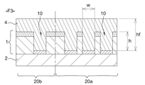
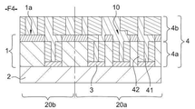
도 1a 내지 1g는 본 발명의 주 실시에 따라, 기판 표면상에 패턴을 만들기 위한 방법의 단계들의 단면 뷰를 나타낸다.
도 2는 가이드 내의 패턴들의 밀도의 함수로서 조립 가이드 내의 블록 공중합체의 두께 변화를 보여주며, 도 2는 선행 기술 방법(테스트 1번)에 따른 침적 단계후이며, 본 발명에 따른 방법(테스트 2번 및 3번)의 시닝 단계 후이다:
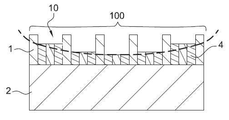
도 3a 및 도 3b는 조립 가이드 내의 블록 공중합체의 층을 나타내며, 도 3은 선행기술 방법에 따른 침적 단계 후이며, 본 발명에 따른 시닝 단계 후이다.
보다 분명하게 하기 위해, 모든 도면 내에서, 동일 또는 유사한 요소들이 동일한 기준 표시들에 의해 표시될 수 있다.


Claims (17)
- 하기의 단계를 포함하는 블록 공중합체 자기 조립에 의해 기판 표면 상(2)에 최종 패턴(21)을 제조하기 위한 방법:
상기 기판의 제 1 및 제 2 영역 (20a, 20b)상에 조립 가이드(1)를 형성하는 단계, 상기 조립 가이드는 기준 표면(1a)과 비교하여, 제 1 영역 (20a)이 제 2 영역(20b) 보다 더 큰 오프닝 비율(opening ratio)를 갖는 오프닝들(10)을 가지며;
블록 공중합체 층 (4)이 상기 조립 가이드 (1)를 완전히 채우고, 상기 기준 표면 (1a) 상에 과도-두께(over-thickness)를 형성하도록, 상기 기판 (2) 상에 블록 공중합체 층 (4)을 침적하는 단계,
상기 블록 공중합체를 조립(assembling) 하는 단계(F4), 상기 조립 단계에 의해, 상기 조립 가이드 (1)의 오프닝들 (10) 내에 상기 블록 공중합체 층의 조직화된 부분(4a)이 만들어지며;
상기 블록 공중합체의 조직화된 부분(4a)에 대응되는 두께에 도달할 때까지, 상기 블록 공중합체 층 (4)을 균일하게 시닝(thinning)하는 단계(F5),
상기 조립된 블록 공중합체의 상들(41) 중 하나를 제거하는 단계, 상기 제거 단계에 의해 복수의 초기 패턴들(43)이 상기 블록 공중합체 층(42)내로 연장되며; 및
상기 최종 패턴들(21)을 형성하기 위해, 상기 블록 공중합체 층 (42)의 초기 패턴들(43)을 상기 기판 (2)으로 전달(transfer)하는 단계(F7). - 제 1항에 있어서, 상기 블록 공중합체 층(4)의 상기 침적 단계(F3)는 스핀 코팅에 의해 수행되는 것을 특징으로 하는 방법.
- 제 1항 또는 제 2항에 있어서, 상기 블록 공중합체는 적어도 하나의 스티렌 유도체 또는 메타크릴레이트 유도체를 포함하는 것을 특징으로 하는 방법.
- 제 1항 내지 3항 중 어느 한 항에 있어서, 상기 블록 공중합체 층(4)의 시닝 단계 (F5)는 플라즈마 에칭에 의해 수행되는 것을 특징으로 하는 방법.
- 제 4항에 있어서, 상기 블록 공중합체 층(4)의 시닝 단계(F5) 및 상기 조립된 블록 공중합체의 상들 (41) 중 하나를 제거하는 단계(F6)는 동일한 플라즈마 에칭 장치 내에서 수행되는 것을 특징으로 하는 방법.
- 제 5항에 있어서, 상기 블록 공중합체 층(4)의 시닝 단계(F5) 및 상기 조립된 블록 공중합체의 상들(41) 중 하나를 제거하는 단계(F6)는 Ar/O2, SF6, CxFy, N2/H2, CO/O2, CO/H2, CH4/O2, CxFy/O2, CHxFy/O2, CxFy/H2, CHxFy/H2 및 CxHy/H2로 부터 선택된 단일한 플라즈마를 사용해서 동시에 수행되는 것을 특징으로 하는 방법.
- 제 5항에 있어서, 상기 상기 블록 공중합체 층(4)의 시닝 단계 (F5) 및 상기 조립된 블록 공중합체의 상들 (41) 중 하나를 제거하는 단계(F6)는 다른 타입의 플라즈마들을 연속 단계로 사용하거나 또는 적어도 2개의 플라즈마들을 교대로 사용해서 수행되는 것을 특징으로 하는 방법.
- 제 1항 내지 7항 중 어느 한 항에 있어서, 상기 공중합체 층(4)의 시닝 단계는 화학적 기계적 평탄화(planarization)에 의해 수행되는 것을 특징으로 하는 방법.
- 제 1항 내지 8항 중 어느 한 항에 있어서, 상기 조립 가이드 (1)는 상기 기판 (2) 상에 배열된 마스크 중으로 형성되고, 포토리소그래피 및/또는 에칭에 의해 텍스쳐되는 것(textured)을 특징으로 하는 방법.
- 제 9항에 있어서, 상기 마스크(1)는 상기 기판(2)에 접촉하는 제 1 탄소 층(11) 및 상기 제 1 탄소 층(11) 상에 배열된 제 2 반사 방지 실리콘 풍부 층(12)을 포함하고, 상기 반사 방지 실리콘 풍부 층(12)는 상기 조립된 블록 공중합체 층의 시닝 단계(F5) 동안, 정지층(stop layer)으로서 작용하는 것을 특징으로 하는 방법.
- 제 1항 내지 10항 중 어느 한 항에 있어서, 상기 조립 가이드(1)는 상기 기판 (2)의 제 1 및 제 2 영역(20a, 20b) 사이에 분포된 가이딩 패턴들(10)을 형성하는 복수의 오프닝들을 포함하는 것을 특징으로 하는 방법.
- 제 11항에 있어서, 상기 가이딩 패턴(10)은 5 nm 내지 1000 nm로 포함되는 높이를 가지는 것을 특징으로 하는 방법.
- 제 11항 또는 제 12항에 있어서, 상기 가이딩 패턴들(10)의 표면은 상기 하나 이상의 블록 공중합체 블록들에 대해 특정 친화도(affinity)를 가지는 것을 특징으로 하는 방법.
- 제 11항 또는 제 12항에 있어서, 상기 가이딩 패턴들(10)의 바닥(bottom)은 상기 블록 공중합체의 블록들에 비해 중성(netural)이며, 여기에서 상기 가이딩 패턴들(10)의 측면들은 블록 공중합체의 하나이상의 블록들에 대해 특정 친화도를 가지는 것을 특징으로 하는 방법.
- 제 11항 또는 제 12항에 있어서, 상기 가이딩 패턴들(10)의 표면은 상기 블록 공중합체의 하나 이상의 블록들에 비해 중성인 것을 특징으로 하는 방법.
- 제 13항 또는 제 14항에 있어서, 상기 블록 공중합체의 하나 이상의 블록들에 대한 조립 가이드(1)의 특정 친화도는 하나 이상의 호모폴리머들의 그래프팅에 의해 얻어지는 것을 특징으로 하는 방법.
- 제 14항 또는 제 15항에 있어서, 상기 조립 가이드 (1)의 중성화는 랜덤 공중합체의 그래프팅에 의해 얻어지는 것을 특징으로 하는 방법.
Applications Claiming Priority (2)
| Application Number | Priority Date | Filing Date | Title |
|---|---|---|---|
| FR1458748A FR3025937B1 (fr) | 2014-09-16 | 2014-09-16 | Procede de grapho-epitaxie pour realiser des motifs a la surface d'un substrat |
| FR1458748 | 2014-09-16 |
Publications (2)
| Publication Number | Publication Date |
|---|---|
| KR20160032702A true KR20160032702A (ko) | 2016-03-24 |
| KR102497635B1 KR102497635B1 (ko) | 2023-02-08 |
Family
ID=51842615
Family Applications (1)
| Application Number | Title | Priority Date | Filing Date |
|---|---|---|---|
| KR1020150131079A Active KR102497635B1 (ko) | 2014-09-16 | 2015-09-16 | 기판 표면상에 패턴을 제조하기 위한 그라포-에피택시 방법 |
Country Status (6)
| Country | Link |
|---|---|
| US (1) | US9535329B2 (ko) |
| EP (1) | EP2998981B1 (ko) |
| JP (1) | JP6735544B2 (ko) |
| KR (1) | KR102497635B1 (ko) |
| FR (1) | FR3025937B1 (ko) |
| TW (1) | TWI678598B (ko) |
Cited By (5)
| Publication number | Priority date | Publication date | Assignee | Title |
|---|---|---|---|---|
| WO2018073550A1 (fr) * | 2016-10-21 | 2018-04-26 | Commissariat A L'energie Atomique Et Aux Energies Alternatives | Procédé de formation d'un guide d'assemblage fonctionnalisé |
| KR20190000918A (ko) * | 2016-05-23 | 2019-01-03 | 도쿄엘렉트론가부시키가이샤 | 다중 재료를 갖는 층을 사용하여 기판을 패터닝하는 방법 |
| KR20190008024A (ko) * | 2017-07-14 | 2019-01-23 | 주식회사 엘지화학 | 블록 공중합체 막의 평탄화 방법 및 패턴 형성 방법 |
| KR20200020229A (ko) * | 2018-08-16 | 2020-02-26 | 주식회사 엘지화학 | 기판의 제조 방법 |
| KR20230113756A (ko) * | 2020-12-02 | 2023-08-01 | 도쿄엘렉트론가부시키가이샤 | 패터닝된 기판 상에 형성된 개구부 내의 충전 재료를 함입하기 위한 방법 |
Families Citing this family (11)
| Publication number | Priority date | Publication date | Assignee | Title |
|---|---|---|---|---|
| TWI723052B (zh) * | 2015-10-23 | 2021-04-01 | 日商東京威力科創股份有限公司 | 基板處理方法、程式及電腦記憶媒體 |
| FR3051966B1 (fr) | 2016-05-27 | 2018-11-09 | Commissariat A L'energie Atomique Et Aux Energies Alternatives | Procede de formation d’un motif de guidage fonctionnalise pour un procede de grapho-epitaxie |
| FR3051964B1 (fr) | 2016-05-27 | 2018-11-09 | Commissariat A L'energie Atomique Et Aux Energies Alternatives | Procede de formation d’un motif de guidage fonctionnalise pour un procede de grapho-epitaxie |
| FR3051965A1 (fr) | 2016-05-27 | 2017-12-01 | Commissariat Energie Atomique | Procede de formation d’un motif de guidage fonctionnalise pour un procede de grapho-epitaxie |
| FR3056334B1 (fr) | 2016-09-22 | 2018-09-28 | Commissariat A L'energie Atomique Et Aux Energies Alternatives | Procede pour augmenter la contrainte dans une region semi-conductrice destinee a former un canal de transistor |
| US10825683B2 (en) * | 2017-06-07 | 2020-11-03 | Imec Vzw | Directed self-assembly of block copolymers |
| FR3069339B1 (fr) * | 2017-07-21 | 2021-05-14 | Arkema France | Procede de controle de l'orientation des nano-domaines d'un copolymere a blocs |
| FR3069340A1 (fr) * | 2017-07-21 | 2019-01-25 | Arkema France | Procede de controle de l'orientation des nano-domaines d'un copolymere a blocs |
| US11613068B2 (en) | 2017-09-13 | 2023-03-28 | Lg Chem, Ltd. | Preparation method of patterned substrate |
| KR102582668B1 (ko) * | 2018-10-01 | 2023-09-25 | 삼성전자주식회사 | 집적회로 소자의 제조 방법 |
| JP2020119929A (ja) | 2019-01-21 | 2020-08-06 | キオクシア株式会社 | 半導体装置 |
Citations (7)
| Publication number | Priority date | Publication date | Assignee | Title |
|---|---|---|---|---|
| US20080182402A1 (en) * | 2007-01-26 | 2008-07-31 | International Business Machines Corporation | Sub-lithographic interconnect patterning using self-assembling polymers |
| JP2010522643A (ja) * | 2007-02-08 | 2010-07-08 | マイクロン テクノロジー, インク. | サブリソグラフィックパターニングのためにブロック共重合体自己集合を使用する方法 |
| JP2011522707A (ja) * | 2008-02-05 | 2011-08-04 | インターナショナル・ビジネス・マシーンズ・コーポレーション | ナノスケール構造及びその製造方法 |
| JP2013073974A (ja) * | 2011-09-26 | 2013-04-22 | Toshiba Corp | パターン形成方法 |
| JP2014022550A (ja) * | 2012-07-18 | 2014-02-03 | Toshiba Corp | パターン形成方法 |
| JP2014070154A (ja) * | 2012-09-28 | 2014-04-21 | Fujifilm Corp | パターン形成用自己組織化組成物、それを用いたブロックコポリマーの自己組織化によるパターン形成方法、及びパターン |
| JP2014135313A (ja) * | 2013-01-08 | 2014-07-24 | Dainippon Printing Co Ltd | インプリントモールドの製造方法 |
Family Cites Families (7)
| Publication number | Priority date | Publication date | Assignee | Title |
|---|---|---|---|---|
| JP4673266B2 (ja) * | 2006-08-03 | 2011-04-20 | 日本電信電話株式会社 | パターン形成方法及びモールド |
| JP5537400B2 (ja) * | 2010-12-22 | 2014-07-02 | 株式会社東芝 | パターン形成方法及び装置 |
| JP5979660B2 (ja) * | 2012-02-09 | 2016-08-24 | 東京応化工業株式会社 | コンタクトホールパターンの形成方法 |
| JP5973763B2 (ja) * | 2012-03-28 | 2016-08-23 | 東京エレクトロン株式会社 | 自己組織化可能なブロック・コポリマーを用いて周期パターン形成する方法及び装置 |
| JP5856550B2 (ja) * | 2012-08-21 | 2016-02-09 | 株式会社東芝 | パターン形成方法 |
| JP2014090029A (ja) * | 2012-10-29 | 2014-05-15 | Panasonic Corp | パターン形成方法及びフォトマスク |
| KR101993255B1 (ko) * | 2013-01-07 | 2019-06-26 | 삼성전자주식회사 | 콘택 홀 형성 방법 |
-
2014
- 2014-09-16 FR FR1458748A patent/FR3025937B1/fr not_active Expired - Fee Related
-
2015
- 2015-09-11 EP EP15184773.8A patent/EP2998981B1/fr active Active
- 2015-09-15 US US14/854,951 patent/US9535329B2/en active Active
- 2015-09-15 TW TW104130451A patent/TWI678598B/zh active
- 2015-09-15 JP JP2015181438A patent/JP6735544B2/ja active Active
- 2015-09-16 KR KR1020150131079A patent/KR102497635B1/ko active Active
Patent Citations (7)
| Publication number | Priority date | Publication date | Assignee | Title |
|---|---|---|---|---|
| US20080182402A1 (en) * | 2007-01-26 | 2008-07-31 | International Business Machines Corporation | Sub-lithographic interconnect patterning using self-assembling polymers |
| JP2010522643A (ja) * | 2007-02-08 | 2010-07-08 | マイクロン テクノロジー, インク. | サブリソグラフィックパターニングのためにブロック共重合体自己集合を使用する方法 |
| JP2011522707A (ja) * | 2008-02-05 | 2011-08-04 | インターナショナル・ビジネス・マシーンズ・コーポレーション | ナノスケール構造及びその製造方法 |
| JP2013073974A (ja) * | 2011-09-26 | 2013-04-22 | Toshiba Corp | パターン形成方法 |
| JP2014022550A (ja) * | 2012-07-18 | 2014-02-03 | Toshiba Corp | パターン形成方法 |
| JP2014070154A (ja) * | 2012-09-28 | 2014-04-21 | Fujifilm Corp | パターン形成用自己組織化組成物、それを用いたブロックコポリマーの自己組織化によるパターン形成方法、及びパターン |
| JP2014135313A (ja) * | 2013-01-08 | 2014-07-24 | Dainippon Printing Co Ltd | インプリントモールドの製造方法 |
Cited By (7)
| Publication number | Priority date | Publication date | Assignee | Title |
|---|---|---|---|---|
| KR20190000918A (ko) * | 2016-05-23 | 2019-01-03 | 도쿄엘렉트론가부시키가이샤 | 다중 재료를 갖는 층을 사용하여 기판을 패터닝하는 방법 |
| WO2018073550A1 (fr) * | 2016-10-21 | 2018-04-26 | Commissariat A L'energie Atomique Et Aux Energies Alternatives | Procédé de formation d'un guide d'assemblage fonctionnalisé |
| FR3057991A1 (fr) * | 2016-10-21 | 2018-04-27 | Commissariat A L'energie Atomique Et Aux Energies Alternatives | Procede de formation d’un guide d’assemblage fonctionnalise |
| US10784108B2 (en) | 2016-10-21 | 2020-09-22 | Commissariat A L'energie Atomique Et Aux Energies Alternatives | Method for forming a functionalised assembly guide |
| KR20190008024A (ko) * | 2017-07-14 | 2019-01-23 | 주식회사 엘지화학 | 블록 공중합체 막의 평탄화 방법 및 패턴 형성 방법 |
| KR20200020229A (ko) * | 2018-08-16 | 2020-02-26 | 주식회사 엘지화학 | 기판의 제조 방법 |
| KR20230113756A (ko) * | 2020-12-02 | 2023-08-01 | 도쿄엘렉트론가부시키가이샤 | 패터닝된 기판 상에 형성된 개구부 내의 충전 재료를 함입하기 위한 방법 |
Also Published As
| Publication number | Publication date |
|---|---|
| EP2998981B1 (fr) | 2018-01-31 |
| EP2998981A1 (fr) | 2016-03-23 |
| US20160077439A1 (en) | 2016-03-17 |
| TW201621469A (zh) | 2016-06-16 |
| JP2016105455A (ja) | 2016-06-09 |
| FR3025937B1 (fr) | 2017-11-24 |
| JP6735544B2 (ja) | 2020-08-05 |
| TWI678598B (zh) | 2019-12-01 |
| KR102497635B1 (ko) | 2023-02-08 |
| FR3025937A1 (fr) | 2016-03-18 |
| US9535329B2 (en) | 2017-01-03 |
Similar Documents
| Publication | Publication Date | Title |
|---|---|---|
| KR102497635B1 (ko) | 기판 표면상에 패턴을 제조하기 위한 그라포-에피택시 방법 | |
| US9738765B2 (en) | Hybrid topographical and chemical pre-patterns for directed self-assembly of block copolymers | |
| KR102047140B1 (ko) | 블록-공중합체를 이용하는 에칭 방법 | |
| US9552988B2 (en) | Tone inverted directed self-assembly (DSA) fin patterning | |
| US10490402B2 (en) | UV-assisted stripping of hardened photoresist to create chemical templates for directed self-assembly | |
| JP7340331B2 (ja) | 化学的ガイディング構造を基板上に形成するための方法及び化学的エピタキシー方法 | |
| US10081740B2 (en) | Directed self-assembly | |
| US9991115B2 (en) | Directed self-assembly using trench assisted chemoepitaxy | |
| US10784108B2 (en) | Method for forming a functionalised assembly guide | |
| US20210088897A1 (en) | Method for forming a chemical guiding structure on a substrate and chemoepitaxy method | |
| US9947597B2 (en) | Defectivity metrology during DSA patterning | |
| US10928725B2 (en) | Method for the directed self-assembly of a block copolymer by graphoepitaxy |
Legal Events
| Date | Code | Title | Description |
|---|---|---|---|
| PA0109 | Patent application |
St.27 status event code: A-0-1-A10-A12-nap-PA0109 |
|
| PG1501 | Laying open of application |
St.27 status event code: A-1-1-Q10-Q12-nap-PG1501 |
|
| P22-X000 | Classification modified |
St.27 status event code: A-2-2-P10-P22-nap-X000 |
|
| A201 | Request for examination | ||
| P11-X000 | Amendment of application requested |
St.27 status event code: A-2-2-P10-P11-nap-X000 |
|
| P13-X000 | Application amended |
St.27 status event code: A-2-2-P10-P13-nap-X000 |
|
| PA0201 | Request for examination |
St.27 status event code: A-1-2-D10-D11-exm-PA0201 |
|
| E902 | Notification of reason for refusal | ||
| PE0902 | Notice of grounds for rejection |
St.27 status event code: A-1-2-D10-D21-exm-PE0902 |
|
| E13-X000 | Pre-grant limitation requested |
St.27 status event code: A-2-3-E10-E13-lim-X000 |
|
| P11-X000 | Amendment of application requested |
St.27 status event code: A-2-2-P10-P11-nap-X000 |
|
| P13-X000 | Application amended |
St.27 status event code: A-2-2-P10-P13-nap-X000 |
|
| R17-X000 | Change to representative recorded |
St.27 status event code: A-3-3-R10-R17-oth-X000 |
|
| E701 | Decision to grant or registration of patent right | ||
| PE0701 | Decision of registration |
St.27 status event code: A-1-2-D10-D22-exm-PE0701 |
|
| P22-X000 | Classification modified |
St.27 status event code: A-2-2-P10-P22-nap-X000 |
|
| P22-X000 | Classification modified |
St.27 status event code: A-2-2-P10-P22-nap-X000 |
|
| PR0701 | Registration of establishment |
St.27 status event code: A-2-4-F10-F11-exm-PR0701 |
|
| PR1002 | Payment of registration fee |
St.27 status event code: A-2-2-U10-U11-oth-PR1002 Fee payment year number: 1 |
|
| PG1601 | Publication of registration |
St.27 status event code: A-4-4-Q10-Q13-nap-PG1601 |
|
| P22-X000 | Classification modified |
St.27 status event code: A-4-4-P10-P22-nap-X000 |