KR20160041969A - 멀티-다이 미세 그레인 집적된 전압 조정 - Google Patents
멀티-다이 미세 그레인 집적된 전압 조정 Download PDFInfo
- Publication number
- KR20160041969A KR20160041969A KR1020167005750A KR20167005750A KR20160041969A KR 20160041969 A KR20160041969 A KR 20160041969A KR 1020167005750 A KR1020167005750 A KR 1020167005750A KR 20167005750 A KR20167005750 A KR 20167005750A KR 20160041969 A KR20160041969 A KR 20160041969A
- Authority
- KR
- South Korea
- Prior art keywords
- semiconductor device
- passive
- power
- terminals
- semiconductor
- Prior art date
- Legal status (The legal status is an assumption and is not a legal conclusion. Google has not performed a legal analysis and makes no representation as to the accuracy of the status listed.)
- Granted
Links
Images


Classifications
-
- H—ELECTRICITY
- H01—ELECTRIC ELEMENTS
- H01G—CAPACITORS; CAPACITORS, RECTIFIERS, DETECTORS, SWITCHING DEVICES, LIGHT-SENSITIVE OR TEMPERATURE-SENSITIVE DEVICES OF THE ELECTROLYTIC TYPE
- H01G4/00—Fixed capacitors; Processes of their manufacture
- H01G4/002—Details
- H01G4/228—Terminals
-
- H01L25/0657—
-
- H—ELECTRICITY
- H01—ELECTRIC ELEMENTS
- H01G—CAPACITORS; CAPACITORS, RECTIFIERS, DETECTORS, SWITCHING DEVICES, LIGHT-SENSITIVE OR TEMPERATURE-SENSITIVE DEVICES OF THE ELECTROLYTIC TYPE
- H01G4/00—Fixed capacitors; Processes of their manufacture
- H01G4/002—Details
- H01G4/228—Terminals
- H01G4/232—Terminals electrically connecting two or more layers of a stacked or rolled capacitor
-
- H—ELECTRICITY
- H01—ELECTRIC ELEMENTS
- H01G—CAPACITORS; CAPACITORS, RECTIFIERS, DETECTORS, SWITCHING DEVICES, LIGHT-SENSITIVE OR TEMPERATURE-SENSITIVE DEVICES OF THE ELECTROLYTIC TYPE
- H01G4/00—Fixed capacitors; Processes of their manufacture
- H01G4/38—Multiple capacitors, i.e. structural combinations of fixed capacitors
-
- H—ELECTRICITY
- H01—ELECTRIC ELEMENTS
- H01G—CAPACITORS; CAPACITORS, RECTIFIERS, DETECTORS, SWITCHING DEVICES, LIGHT-SENSITIVE OR TEMPERATURE-SENSITIVE DEVICES OF THE ELECTROLYTIC TYPE
- H01G4/00—Fixed capacitors; Processes of their manufacture
- H01G4/40—Structural combinations of fixed capacitors with other electric elements, the structure mainly consisting of a capacitor, e.g. RC combinations
-
- H01L24/32—
-
- H01L24/48—
-
- H01L25/0652—
-
- H01L25/105—
-
- H01L27/101—
-
- H—ELECTRICITY
- H10—SEMICONDUCTOR DEVICES; ELECTRIC SOLID-STATE DEVICES NOT OTHERWISE PROVIDED FOR
- H10D—INORGANIC ELECTRIC SEMICONDUCTOR DEVICES
- H10D1/00—Resistors, capacitors or inductors
- H10D1/60—Capacitors
- H10D1/68—Capacitors having no potential barriers
-
- H—ELECTRICITY
- H10—SEMICONDUCTOR DEVICES; ELECTRIC SOLID-STATE DEVICES NOT OTHERWISE PROVIDED FOR
- H10D—INORGANIC ELECTRIC SEMICONDUCTOR DEVICES
- H10D1/00—Resistors, capacitors or inductors
- H10D1/60—Capacitors
- H10D1/68—Capacitors having no potential barriers
- H10D1/692—Electrodes
-
- H—ELECTRICITY
- H10—SEMICONDUCTOR DEVICES; ELECTRIC SOLID-STATE DEVICES NOT OTHERWISE PROVIDED FOR
- H10W—GENERIC PACKAGES, INTERCONNECTIONS, CONNECTORS OR OTHER CONSTRUCTIONAL DETAILS OF DEVICES COVERED BY CLASS H10
- H10W20/00—Interconnections in chips, wafers or substrates
- H10W20/20—Interconnections within wafers or substrates, e.g. through-silicon vias [TSV]
-
- H—ELECTRICITY
- H10—SEMICONDUCTOR DEVICES; ELECTRIC SOLID-STATE DEVICES NOT OTHERWISE PROVIDED FOR
- H10W—GENERIC PACKAGES, INTERCONNECTIONS, CONNECTORS OR OTHER CONSTRUCTIONAL DETAILS OF DEVICES COVERED BY CLASS H10
- H10W44/00—Electrical arrangements for controlling or matching impedance
- H10W44/601—Capacitive arrangements
-
- H—ELECTRICITY
- H10—SEMICONDUCTOR DEVICES; ELECTRIC SOLID-STATE DEVICES NOT OTHERWISE PROVIDED FOR
- H10W—GENERIC PACKAGES, INTERCONNECTIONS, CONNECTORS OR OTHER CONSTRUCTIONAL DETAILS OF DEVICES COVERED BY CLASS H10
- H10W70/00—Package substrates; Interposers; Redistribution layers [RDL]
- H10W70/60—Insulating or insulated package substrates; Interposers; Redistribution layers
- H10W70/67—Insulating or insulated package substrates; Interposers; Redistribution layers characterised by their insulating layers or insulating parts
- H10W70/68—Shapes or dispositions thereof
-
- H—ELECTRICITY
- H10—SEMICONDUCTOR DEVICES; ELECTRIC SOLID-STATE DEVICES NOT OTHERWISE PROVIDED FOR
- H10W—GENERIC PACKAGES, INTERCONNECTIONS, CONNECTORS OR OTHER CONSTRUCTIONAL DETAILS OF DEVICES COVERED BY CLASS H10
- H10W90/00—Package configurations
-
- H—ELECTRICITY
- H10—SEMICONDUCTOR DEVICES; ELECTRIC SOLID-STATE DEVICES NOT OTHERWISE PROVIDED FOR
- H10W—GENERIC PACKAGES, INTERCONNECTIONS, CONNECTORS OR OTHER CONSTRUCTIONAL DETAILS OF DEVICES COVERED BY CLASS H10
- H10W90/00—Package configurations
- H10W90/701—Package configurations characterised by the relative positions of pads or connectors relative to package parts
-
- H01L2224/0401—
-
- H01L2225/06513—
-
- H01L2225/06517—
-
- H01L2225/1023—
-
- H—ELECTRICITY
- H10—SEMICONDUCTOR DEVICES; ELECTRIC SOLID-STATE DEVICES NOT OTHERWISE PROVIDED FOR
- H10B—ELECTRONIC MEMORY DEVICES
- H10B12/00—Dynamic random access memory [DRAM] devices
-
- H—ELECTRICITY
- H10—SEMICONDUCTOR DEVICES; ELECTRIC SOLID-STATE DEVICES NOT OTHERWISE PROVIDED FOR
- H10W—GENERIC PACKAGES, INTERCONNECTIONS, CONNECTORS OR OTHER CONSTRUCTIONAL DETAILS OF DEVICES COVERED BY CLASS H10
- H10W70/00—Package substrates; Interposers; Redistribution layers [RDL]
- H10W70/60—Insulating or insulated package substrates; Interposers; Redistribution layers
- H10W70/62—Insulating or insulated package substrates; Interposers; Redistribution layers characterised by their interconnections
- H10W70/63—Vias, e.g. via plugs
- H10W70/635—Through-vias
-
- H—ELECTRICITY
- H10—SEMICONDUCTOR DEVICES; ELECTRIC SOLID-STATE DEVICES NOT OTHERWISE PROVIDED FOR
- H10W—GENERIC PACKAGES, INTERCONNECTIONS, CONNECTORS OR OTHER CONSTRUCTIONAL DETAILS OF DEVICES COVERED BY CLASS H10
- H10W70/00—Package substrates; Interposers; Redistribution layers [RDL]
- H10W70/60—Insulating or insulated package substrates; Interposers; Redistribution layers
- H10W70/62—Insulating or insulated package substrates; Interposers; Redistribution layers characterised by their interconnections
- H10W70/65—Shapes or dispositions of interconnections
- H10W70/654—Top-view layouts
- H10W70/655—Fan-out layouts
-
- H—ELECTRICITY
- H10—SEMICONDUCTOR DEVICES; ELECTRIC SOLID-STATE DEVICES NOT OTHERWISE PROVIDED FOR
- H10W—GENERIC PACKAGES, INTERCONNECTIONS, CONNECTORS OR OTHER CONSTRUCTIONAL DETAILS OF DEVICES COVERED BY CLASS H10
- H10W70/00—Package substrates; Interposers; Redistribution layers [RDL]
- H10W70/60—Insulating or insulated package substrates; Interposers; Redistribution layers
- H10W70/67—Insulating or insulated package substrates; Interposers; Redistribution layers characterised by their insulating layers or insulating parts
- H10W70/68—Shapes or dispositions thereof
- H10W70/682—Shapes or dispositions thereof comprising holes having chips therein
-
- H—ELECTRICITY
- H10—SEMICONDUCTOR DEVICES; ELECTRIC SOLID-STATE DEVICES NOT OTHERWISE PROVIDED FOR
- H10W—GENERIC PACKAGES, INTERCONNECTIONS, CONNECTORS OR OTHER CONSTRUCTIONAL DETAILS OF DEVICES COVERED BY CLASS H10
- H10W72/00—Interconnections or connectors in packages
-
- H—ELECTRICITY
- H10—SEMICONDUCTOR DEVICES; ELECTRIC SOLID-STATE DEVICES NOT OTHERWISE PROVIDED FOR
- H10W—GENERIC PACKAGES, INTERCONNECTIONS, CONNECTORS OR OTHER CONSTRUCTIONAL DETAILS OF DEVICES COVERED BY CLASS H10
- H10W72/00—Interconnections or connectors in packages
- H10W72/20—Bump connectors, e.g. solder bumps or copper pillars; Dummy bumps; Thermal bumps
- H10W72/221—Structures or relative sizes
- H10W72/227—Multiple bumps having different sizes
-
- H—ELECTRICITY
- H10—SEMICONDUCTOR DEVICES; ELECTRIC SOLID-STATE DEVICES NOT OTHERWISE PROVIDED FOR
- H10W—GENERIC PACKAGES, INTERCONNECTIONS, CONNECTORS OR OTHER CONSTRUCTIONAL DETAILS OF DEVICES COVERED BY CLASS H10
- H10W72/00—Interconnections or connectors in packages
- H10W72/20—Bump connectors, e.g. solder bumps or copper pillars; Dummy bumps; Thermal bumps
- H10W72/241—Dispositions, e.g. layouts
- H10W72/244—Dispositions, e.g. layouts relative to underlying supporting features, e.g. bond pads, RDLs or vias
-
- H—ELECTRICITY
- H10—SEMICONDUCTOR DEVICES; ELECTRIC SOLID-STATE DEVICES NOT OTHERWISE PROVIDED FOR
- H10W—GENERIC PACKAGES, INTERCONNECTIONS, CONNECTORS OR OTHER CONSTRUCTIONAL DETAILS OF DEVICES COVERED BY CLASS H10
- H10W72/00—Interconnections or connectors in packages
- H10W72/20—Bump connectors, e.g. solder bumps or copper pillars; Dummy bumps; Thermal bumps
- H10W72/241—Dispositions, e.g. layouts
- H10W72/247—Dispositions of multiple bumps
- H10W72/248—Top-view layouts, e.g. mirror arrays
-
- H—ELECTRICITY
- H10—SEMICONDUCTOR DEVICES; ELECTRIC SOLID-STATE DEVICES NOT OTHERWISE PROVIDED FOR
- H10W—GENERIC PACKAGES, INTERCONNECTIONS, CONNECTORS OR OTHER CONSTRUCTIONAL DETAILS OF DEVICES COVERED BY CLASS H10
- H10W72/00—Interconnections or connectors in packages
- H10W72/20—Bump connectors, e.g. solder bumps or copper pillars; Dummy bumps; Thermal bumps
- H10W72/29—Bond pads specially adapted therefor
-
- H—ELECTRICITY
- H10—SEMICONDUCTOR DEVICES; ELECTRIC SOLID-STATE DEVICES NOT OTHERWISE PROVIDED FOR
- H10W—GENERIC PACKAGES, INTERCONNECTIONS, CONNECTORS OR OTHER CONSTRUCTIONAL DETAILS OF DEVICES COVERED BY CLASS H10
- H10W72/00—Interconnections or connectors in packages
- H10W72/50—Bond wires
- H10W72/551—Materials of bond wires
-
- H—ELECTRICITY
- H10—SEMICONDUCTOR DEVICES; ELECTRIC SOLID-STATE DEVICES NOT OTHERWISE PROVIDED FOR
- H10W—GENERIC PACKAGES, INTERCONNECTIONS, CONNECTORS OR OTHER CONSTRUCTIONAL DETAILS OF DEVICES COVERED BY CLASS H10
- H10W72/00—Interconnections or connectors in packages
- H10W72/851—Dispositions of multiple connectors or interconnections
- H10W72/874—On different surfaces
- H10W72/884—Die-attach connectors and bond wires
-
- H—ELECTRICITY
- H10—SEMICONDUCTOR DEVICES; ELECTRIC SOLID-STATE DEVICES NOT OTHERWISE PROVIDED FOR
- H10W—GENERIC PACKAGES, INTERCONNECTIONS, CONNECTORS OR OTHER CONSTRUCTIONAL DETAILS OF DEVICES COVERED BY CLASS H10
- H10W90/00—Package configurations
- H10W90/20—Configurations of stacked chips
- H10W90/291—Configurations of stacked chips characterised by containers, encapsulations, or other housings for the stacked chips
-
- H—ELECTRICITY
- H10—SEMICONDUCTOR DEVICES; ELECTRIC SOLID-STATE DEVICES NOT OTHERWISE PROVIDED FOR
- H10W—GENERIC PACKAGES, INTERCONNECTIONS, CONNECTORS OR OTHER CONSTRUCTIONAL DETAILS OF DEVICES COVERED BY CLASS H10
- H10W90/00—Package configurations
- H10W90/701—Package configurations characterised by the relative positions of pads or connectors relative to package parts
- H10W90/721—Package configurations characterised by the relative positions of pads or connectors relative to package parts of bump connectors
- H10W90/722—Package configurations characterised by the relative positions of pads or connectors relative to package parts of bump connectors between stacked chips
-
- H—ELECTRICITY
- H10—SEMICONDUCTOR DEVICES; ELECTRIC SOLID-STATE DEVICES NOT OTHERWISE PROVIDED FOR
- H10W—GENERIC PACKAGES, INTERCONNECTIONS, CONNECTORS OR OTHER CONSTRUCTIONAL DETAILS OF DEVICES COVERED BY CLASS H10
- H10W90/00—Package configurations
- H10W90/701—Package configurations characterised by the relative positions of pads or connectors relative to package parts
- H10W90/721—Package configurations characterised by the relative positions of pads or connectors relative to package parts of bump connectors
- H10W90/724—Package configurations characterised by the relative positions of pads or connectors relative to package parts of bump connectors between a chip and a stacked insulating package substrate, interposer or RDL
-
- H—ELECTRICITY
- H10—SEMICONDUCTOR DEVICES; ELECTRIC SOLID-STATE DEVICES NOT OTHERWISE PROVIDED FOR
- H10W—GENERIC PACKAGES, INTERCONNECTIONS, CONNECTORS OR OTHER CONSTRUCTIONAL DETAILS OF DEVICES COVERED BY CLASS H10
- H10W90/00—Package configurations
- H10W90/701—Package configurations characterised by the relative positions of pads or connectors relative to package parts
- H10W90/721—Package configurations characterised by the relative positions of pads or connectors relative to package parts of bump connectors
- H10W90/728—Package configurations characterised by the relative positions of pads or connectors relative to package parts of bump connectors between a chip and a stacked discrete passive device, e.g. resistors, capacitors or inductors
-
- H—ELECTRICITY
- H10—SEMICONDUCTOR DEVICES; ELECTRIC SOLID-STATE DEVICES NOT OTHERWISE PROVIDED FOR
- H10W—GENERIC PACKAGES, INTERCONNECTIONS, CONNECTORS OR OTHER CONSTRUCTIONAL DETAILS OF DEVICES COVERED BY CLASS H10
- H10W90/00—Package configurations
- H10W90/701—Package configurations characterised by the relative positions of pads or connectors relative to package parts
- H10W90/731—Package configurations characterised by the relative positions of pads or connectors relative to package parts of die-attach connectors
- H10W90/734—Package configurations characterised by the relative positions of pads or connectors relative to package parts of die-attach connectors between a chip and a stacked insulating package substrate, interposer or RDL
-
- H—ELECTRICITY
- H10—SEMICONDUCTOR DEVICES; ELECTRIC SOLID-STATE DEVICES NOT OTHERWISE PROVIDED FOR
- H10W—GENERIC PACKAGES, INTERCONNECTIONS, CONNECTORS OR OTHER CONSTRUCTIONAL DETAILS OF DEVICES COVERED BY CLASS H10
- H10W90/00—Package configurations
- H10W90/701—Package configurations characterised by the relative positions of pads or connectors relative to package parts
- H10W90/751—Package configurations characterised by the relative positions of pads or connectors relative to package parts of bond wires
- H10W90/754—Package configurations characterised by the relative positions of pads or connectors relative to package parts of bond wires between a chip and a stacked insulating package substrate, interposer or RDL
Landscapes
- Engineering & Computer Science (AREA)
- Power Engineering (AREA)
- Manufacturing & Machinery (AREA)
- Microelectronics & Electronic Packaging (AREA)
- Semiconductor Integrated Circuits (AREA)
Abstract
Description
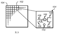
도 1은 반도체 디바이스 패키지의 실시예의 분해도 표현을 도시한다.
도 2는 반도체 디바이스 패키지의 실시예의 측면도 표현을 도시한다.
도 3은 수동 디바이스의 실시예의 표현을 도시한다.
도 4는 구조체의 하나의 가능한 실시예의 예의 확대도를 도시한다.
도 5는 구조체의 다른 가능한 실시예의 예의 표현을 도시한다.
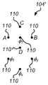
도 6은 도 5에 도시된 구조체를 위한 일반 단자 풋프린트(generic terminal footprint)를 도시한다.
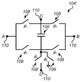
도 7은 커패시터들 및 단자들만을 갖는 구조체의 실시예의 예의 표현을 도시한다.
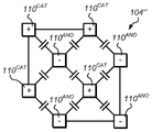
도 8은 구조체들을 사용하여 어레이를 위한 단자 풋프린트의 실시예의 표현을 도시한다.
도 9는 수동 디바이스, 전력 소모 디바이스, 및 메모리 디바이스를 갖는 패키지의 실시예의 측면도 표현을 도시한다.
도 10은 반도체 디바이스 패키지의 다른 실시예의 측면도 표현을 도시한다.
도 11은 반도체 디바이스 패키지의 또 다른 실시예의 측면도 표현을 도시한다.
도 12는 수동 디바이스, 전력 소모 디바이스, 및 메모리 디바이스를 갖는 패키지의 다른 실시예의 측면도 표현을 도시한다.
본 발명은 다양한 수정들과 대안적인 형태들을 허용하지만, 본 발명의 특정 실시예들이 도면에서 예로서 도시되고 본 명세서에서 상세히 설명될 것이다. 도면은 축척대로 도시되지 않을 수 있다. 그에 대한 도면 및 상세한 설명은 본 발명을 개시된 특정 형태로 제한하도록 의도되는 것이 아니며, 반대로, 첨부된 청구범위에 의해 정의되는 바와 같은 본 발명의 기술적 사상 및 범주 내에 있는 모든 수정들, 등가물들 및 대안들을 포괄하려는 의도로 이해하여야 한다.
Claims (15)
- 반도체 디바이스로서,
반도체 기판;
상기 반도체 기판 상에 형성된 복수의 수동 소자 - 상기 수동 소자들은 상기 반도체 기판 상에 어레이로 배열됨 -; 및
상기 수동 소자들을 적어도 하나의 추가 반도체 디바이스에 결합하기 위한 하나 이상의 단자
를 포함하는, 반도체 디바이스. - 제1항에 있어서, 상기 수동 소자들은 커패시터들을 포함하는, 반도체 디바이스.
- 제1항에 있어서, 상기 어레이 내의 상기 수동 소자들 중 2개 이상은 서로 결합되는, 반도체 디바이스.
- 제1항에 있어서, 상기 반도체 기판 상에 형성된 하나 이상의 스위치를 더 포함하는, 반도체 디바이스.
- 제1항에 있어서, 상기 단자들은 상기 수동 소자들 사이에 단락을 방지하기 위하여 최소 거리로 이격되는, 반도체 디바이스.
- 제1항에 있어서, 상기 단자들 중 적어도 하나는 관통 실리콘 비아(TSV)를 포함하는, 반도체 디바이스.
- 제1항에 있어서, 상기 반도체 기판 상에 형성된 메모리 디바이스를 더 포함하는, 반도체 디바이스.
- 반도체 디바이스 패키지로서,
제1 반도체 디바이스 - 상기 제1 반도체 디바이스는,
제1 반도체 기판;
상기 제1 반도체 기판 상에 형성된 하나 이상의 수동 소자; 및
하나 이상의 단자를 포함함 -; 및
상기 단자들 중 하나 이상을 사용하여 상기 제1 반도체 디바이스에 결합되는 제2 반도체 디바이스 - 상기 제2 반도체 디바이스는,
제2 반도체 기판; 및
상기 제2 반도체 기판 상에 형성된 하나 이상의 전류 소모 소자를 포함함 ―
를 포함하는, 반도체 디바이스 패키지. - 제8항에 있어서, 상기 수동 소자들은 상기 제1 반도체 기판 상에 어레이로 배열되는, 반도체 디바이스.
- 제8항에 있어서, 상기 제2 반도체 디바이스는 시스템 온 칩(SOC) 디바이스를 포함하는, 반도체 디바이스.
- 제8항에 있어서, 상기 어레이 내의 상기 수동 소자들 중 2개 이상은 서로 결합되는, 반도체 디바이스.
- 제8항에 있어서, 상기 제2 반도체 기판 상에 형성된 하나 이상의 스위치를 더 포함하는, 반도체 디바이스.
- 제8항에 있어서, 상기 제1 반도체 디바이스는 상기 제1 반도체 기판 상의 금속 라우팅(metal routing)을 포함하고, 상기 금속 라우팅은 상기 제1 반도체 디바이스가 상기 제2 반도체 디바이스에 결합되는 경우 전력 레일(power rail)로서 사용되는, 반도체 디바이스.
- 제8항에 있어서, 상기 제1 반도체 디바이스 및 상기 제2 반도체 디바이스는 상기 제2 세민컨덕터 디바이스가 상기 수동 소자들 및 상기 전류 소모 소자들의 하나 이상의 동작 특성을 정의하도록 결합되는, 반도체 디바이스.
- 제8항에 있어서, 상기 제1 반도체 디바이스 및 상기 제2 반도체 디바이스는 상기 수동 소자들 및 상기 전류 소모 소자들이 하나 이상의 국부화된 전압 조정 구조체로 분리되도록 결합되며, 각각의 국부화된 전압 조정 구조체는 별개의 전압 전력 공급 조정기를 포함하는, 반도체 디바이스.
Applications Claiming Priority (5)
| Application Number | Priority Date | Filing Date | Title |
|---|---|---|---|
| US201361864014P | 2013-08-09 | 2013-08-09 | |
| US61/864,014 | 2013-08-09 | ||
| US14/077,512 | 2013-11-12 | ||
| US14/077,512 US9595526B2 (en) | 2013-08-09 | 2013-11-12 | Multi-die fine grain integrated voltage regulation |
| PCT/US2014/048603 WO2015020836A2 (en) | 2013-08-09 | 2014-07-29 | Multi-die fine grain integrated voltage regulation |
Publications (2)
| Publication Number | Publication Date |
|---|---|
| KR20160041969A true KR20160041969A (ko) | 2016-04-18 |
| KR101819838B1 KR101819838B1 (ko) | 2018-01-17 |
Family
ID=52447943
Family Applications (1)
| Application Number | Title | Priority Date | Filing Date |
|---|---|---|---|
| KR1020167005750A Active KR101819838B1 (ko) | 2013-08-09 | 2014-07-29 | 멀티-다이 미세 그레인 집적된 전압 조정 |
Country Status (8)
| Country | Link |
|---|---|
| US (7) | US9595526B2 (ko) |
| EP (2) | EP4006972A3 (ko) |
| JP (1) | JP6174260B2 (ko) |
| KR (1) | KR101819838B1 (ko) |
| CN (1) | CN105474391B (ko) |
| DE (1) | DE202014011574U1 (ko) |
| TW (1) | TWI529875B (ko) |
| WO (1) | WO2015020836A2 (ko) |
Families Citing this family (22)
| Publication number | Priority date | Publication date | Assignee | Title |
|---|---|---|---|---|
| US9595526B2 (en) | 2013-08-09 | 2017-03-14 | Apple Inc. | Multi-die fine grain integrated voltage regulation |
| US10468381B2 (en) | 2014-09-29 | 2019-11-05 | Apple Inc. | Wafer level integration of passive devices |
| US9971970B1 (en) * | 2015-04-27 | 2018-05-15 | Rigetti & Co, Inc. | Microwave integrated quantum circuits with VIAS and methods for making the same |
| US9935076B1 (en) | 2015-09-30 | 2018-04-03 | Apple Inc. | Structure and method for fabricating a computing system with an integrated voltage regulator module |
| JP2017084961A (ja) * | 2015-10-28 | 2017-05-18 | 株式会社村田製作所 | 集積回路素子の実装構造 |
| US10665579B2 (en) | 2016-02-16 | 2020-05-26 | Xilinx, Inc. | Chip package assembly with power management integrated circuit and integrated circuit die |
| CN107369678A (zh) * | 2016-05-13 | 2017-11-21 | 北京中电网信息技术有限公司 | 一种系统级封装方法及其封装单元 |
| US10242967B2 (en) * | 2017-05-16 | 2019-03-26 | Raytheon Company | Die encapsulation in oxide bonded wafer stack |
| US11121301B1 (en) | 2017-06-19 | 2021-09-14 | Rigetti & Co, Inc. | Microwave integrated quantum circuits with cap wafers and their methods of manufacture |
| MY199714A (en) * | 2017-07-04 | 2023-11-20 | Intel Corp | Stacked dies with passive components within facing recesses |
| US10535394B2 (en) * | 2017-07-20 | 2020-01-14 | Samsung Electronics Co., Ltd. | Memory device including dynamic voltage and frequency scaling switch and method of operating the same |
| US10529407B2 (en) * | 2017-07-20 | 2020-01-07 | Samsung Electronics Co., Ltd. | Memory device including a plurality of power rails and method of operating the same |
| DE102017129611B4 (de) * | 2017-12-12 | 2021-04-22 | RF360 Europe GmbH | Elektrische Vorrichtung mit zwei oder mehr Chipkomponenten |
| KR102679250B1 (ko) * | 2018-09-12 | 2024-06-28 | 엘지이노텍 주식회사 | 연성 회로기판 및 이를 포함하는 칩 패키지, 및 이를 포함하는 전자 디바이스 |
| US10756622B2 (en) | 2018-12-24 | 2020-08-25 | Apple Inc | Power management system switched capacitor voltage regulator with integrated passive device |
| DE102019110716B3 (de) * | 2019-04-25 | 2020-01-16 | Semikron Elektronik Gmbh & Co. Kg | Leistungshalbleitermodul mit Leistungshalbleiterschaltern |
| US20200373224A1 (en) * | 2019-05-21 | 2020-11-26 | Microsoft Technology Licensing, Llc | Through-silicon vias and decoupling capacitance |
| US11710726B2 (en) | 2019-06-25 | 2023-07-25 | Microsoft Technology Licensing, Llc | Through-board power control arrangements for integrated circuit devices |
| KR102766383B1 (ko) | 2019-08-06 | 2025-02-12 | 삼성전자주식회사 | 멀티-코어 시스템 및 그 동작 제어 방법 |
| US11537154B2 (en) | 2020-12-09 | 2022-12-27 | Samsung Electronics Co., Ltd. | Mobile devices and methods controlling power in mobile devices |
| US12300679B2 (en) | 2021-05-17 | 2025-05-13 | Mediatek Inc. | Semiconductor package structure |
| US12431416B2 (en) * | 2022-04-11 | 2025-09-30 | Xilinx, Inc. | Chip package with integrated current control |
Family Cites Families (37)
| Publication number | Priority date | Publication date | Assignee | Title |
|---|---|---|---|---|
| US4080590A (en) * | 1976-03-31 | 1978-03-21 | International Business Machines Corporation | Capacitor storage memory |
| US5786979A (en) * | 1995-12-18 | 1998-07-28 | Douglass; Barry G. | High density inter-chip connections by electromagnetic coupling |
| WO2000079592A1 (fr) * | 1999-06-17 | 2000-12-28 | Hitachi, Ltd. | Composant a semiconducteur et dispositif electronique |
| US6532143B2 (en) * | 2000-12-29 | 2003-03-11 | Intel Corporation | Multiple tier array capacitor |
| US6477034B1 (en) * | 2001-10-03 | 2002-11-05 | Intel Corporation | Interposer substrate with low inductance capacitive paths |
| US7327554B2 (en) * | 2003-03-19 | 2008-02-05 | Ngk Spark Plug Co., Ltd. | Assembly of semiconductor device, interposer and substrate |
| US7190210B2 (en) * | 2004-03-25 | 2007-03-13 | Integral Wave Technologies, Inc. | Switched-capacitor power supply system and method |
| US7446389B2 (en) * | 2004-06-17 | 2008-11-04 | Apple Inc. | Semiconductor die package with internal bypass capacitors |
| US8178901B2 (en) * | 2005-04-28 | 2012-05-15 | St-Ericsson Sa | Integrated circuit assembly with passive integration substrate for power and ground line routing on top of an integrated circuit chip |
| JP4546415B2 (ja) * | 2005-09-01 | 2010-09-15 | 日本特殊陶業株式会社 | 配線基板、セラミックキャパシタ |
| US7692284B2 (en) * | 2005-12-12 | 2010-04-06 | Intel Corporation | Package using array capacitor core |
| US7612984B2 (en) * | 2006-11-01 | 2009-11-03 | Taiwan Semiconductor Manufacturing Company, Ltd. | Layout for capacitor pair with high capacitance matching |
| US20080128854A1 (en) * | 2006-12-04 | 2008-06-05 | Augustine Anne E | Embedded array capacitor with top and bottom exterior surface metallization |
| US8264846B2 (en) * | 2006-12-14 | 2012-09-11 | Intel Corporation | Ceramic package substrate with recessed device |
| US20080157343A1 (en) | 2006-12-29 | 2008-07-03 | Sriram Dattaguru | Ceramic interposer with silicon voltage regulator and array capacitor combination for integrated circuit packages |
| JP4734282B2 (ja) * | 2007-04-23 | 2011-07-27 | 株式会社日立製作所 | 半導体チップおよび半導体装置 |
| CN101682252B (zh) * | 2007-05-10 | 2013-10-23 | Nxp股份有限公司 | 包含可重构电容器单元的直流-直流变换器 |
| US8476735B2 (en) * | 2007-05-29 | 2013-07-02 | Taiwan Semiconductor Manufacturing Company, Ltd. | Programmable semiconductor interposer for electronic package and method of forming |
| JP4429346B2 (ja) * | 2007-08-31 | 2010-03-10 | 富士通株式会社 | 半導体装置及びその製造方法 |
| US7952160B2 (en) | 2007-12-31 | 2011-05-31 | Intel Corporation | Packaged voltage regulator and inductor array |
| US8341434B2 (en) | 2008-02-26 | 2012-12-25 | International Business Machines Corporation | Optimizing voltage on a power plane using a networked voltage regulation module array |
| JP5335931B2 (ja) | 2008-12-26 | 2013-11-06 | メギカ・コーポレイション | 電力管理集積回路を有するチップ・パッケージおよび関連技術 |
| US8242551B2 (en) * | 2009-03-04 | 2012-08-14 | Taiwan Semiconductor Manufacturing Company, Ltd. | Metal-insulator-metal structure for system-on-chip technology |
| US9607935B2 (en) * | 2009-04-21 | 2017-03-28 | Ati Technologies Ulc | Semiconductor chip package with undermount passive devices |
| US8188786B2 (en) * | 2009-09-24 | 2012-05-29 | International Business Machines Corporation | Modularized three-dimensional capacitor array |
| US8558345B2 (en) * | 2009-11-09 | 2013-10-15 | International Business Machines Corporation | Integrated decoupling capacitor employing conductive through-substrate vias |
| US9048112B2 (en) | 2010-06-29 | 2015-06-02 | Qualcomm Incorporated | Integrated voltage regulator with embedded passive device(s) for a stacked IC |
| US9064712B2 (en) * | 2010-08-12 | 2015-06-23 | Freescale Semiconductor Inc. | Monolithic microwave integrated circuit |
| US8716855B2 (en) | 2010-11-10 | 2014-05-06 | Taiwan Semiconductor Manufacturing Company, Ltd. | Integrated circuit system with distributed power supply comprising interposer and voltage regulator module |
| JP2012160693A (ja) * | 2011-01-11 | 2012-08-23 | Kyocera Corp | 積層型半導体パッケージおよび積層型半導体装置 |
| JP2012156184A (ja) * | 2011-01-24 | 2012-08-16 | Nec Corp | 実装基板及びその製造方法 |
| JP2013021269A (ja) * | 2011-07-14 | 2013-01-31 | Ngk Spark Plug Co Ltd | 部品内蔵配線基板 |
| US9337138B1 (en) * | 2012-03-09 | 2016-05-10 | Xilinx, Inc. | Capacitors within an interposer coupled to supply and ground planes of a substrate |
| US20140135545A1 (en) | 2012-11-12 | 2014-05-15 | Uop Llc | Fluid catalytic cracking process |
| US9496211B2 (en) * | 2012-11-21 | 2016-11-15 | Intel Corporation | Logic die and other components embedded in build-up layers |
| US20140252547A1 (en) | 2013-03-08 | 2014-09-11 | Advanced Semiconductor Engineering, Inc. | Semiconductor device having integrated passive device and process for manufacturing the same |
| US9595526B2 (en) | 2013-08-09 | 2017-03-14 | Apple Inc. | Multi-die fine grain integrated voltage regulation |
-
2013
- 2013-11-12 US US14/077,512 patent/US9595526B2/en active Active
-
2014
- 2014-07-29 EP EP22150527.4A patent/EP4006972A3/en not_active Withdrawn
- 2014-07-29 WO PCT/US2014/048603 patent/WO2015020836A2/en not_active Ceased
- 2014-07-29 JP JP2016533324A patent/JP6174260B2/ja active Active
- 2014-07-29 KR KR1020167005750A patent/KR101819838B1/ko active Active
- 2014-07-29 CN CN201480044455.1A patent/CN105474391B/zh active Active
- 2014-07-29 DE DE202014011574.5U patent/DE202014011574U1/de not_active Expired - Lifetime
- 2014-07-29 EP EP14758191.2A patent/EP3031081A2/en not_active Ceased
- 2014-08-08 TW TW103127346A patent/TWI529875B/zh active
-
2017
- 2017-01-31 US US15/420,572 patent/US10056384B2/en active Active
-
2018
- 2018-07-23 US US16/042,582 patent/US10411012B2/en active Active
-
2019
- 2019-08-01 US US16/529,043 patent/US11063046B2/en active Active
-
2021
- 2021-06-25 US US17/358,790 patent/US12068324B2/en active Active
-
2024
- 2024-07-19 US US18/777,726 patent/US20250015033A1/en active Pending
-
2025
- 2025-01-09 US US19/015,233 patent/US20250149489A1/en active Pending
Also Published As
| Publication number | Publication date |
|---|---|
| US20180366466A1 (en) | 2018-12-20 |
| US11063046B2 (en) | 2021-07-13 |
| US20200027881A1 (en) | 2020-01-23 |
| TW201515165A (zh) | 2015-04-16 |
| US10056384B2 (en) | 2018-08-21 |
| KR101819838B1 (ko) | 2018-01-17 |
| EP4006972A3 (en) | 2022-12-28 |
| WO2015020836A2 (en) | 2015-02-12 |
| US20250015033A1 (en) | 2025-01-09 |
| EP3031081A2 (en) | 2016-06-15 |
| US10411012B2 (en) | 2019-09-10 |
| CN105474391A (zh) | 2016-04-06 |
| US20250149489A1 (en) | 2025-05-08 |
| US20170141116A1 (en) | 2017-05-18 |
| US20150041955A1 (en) | 2015-02-12 |
| EP4006972A2 (en) | 2022-06-01 |
| JP6174260B2 (ja) | 2017-08-02 |
| WO2015020836A3 (en) | 2015-04-09 |
| TWI529875B (zh) | 2016-04-11 |
| US9595526B2 (en) | 2017-03-14 |
| JP2016529719A (ja) | 2016-09-23 |
| US12068324B2 (en) | 2024-08-20 |
| CN105474391B (zh) | 2018-08-03 |
| DE202014011574U1 (de) | 2022-06-27 |
| US20210398980A1 (en) | 2021-12-23 |
Similar Documents
| Publication | Publication Date | Title |
|---|---|---|
| KR101819838B1 (ko) | 멀티-다이 미세 그레인 집적된 전압 조정 | |
| KR101614132B1 (ko) | 임베딩된 수동 디바이스(들)를 구비한 통합된 전압 레귤레이터를 포함하는 적층형 ic | |
| US8692368B2 (en) | Integrated voltage regulator method with embedded passive device(s) | |
| US11532613B2 (en) | Structure and method for cooling three-dimensional integrated circuits | |
| CN103972224A (zh) | 具有有源内插器的集成电路封装 | |
| US9312761B2 (en) | Three-D power converter in three distinct strata | |
| TW201346906A (zh) | 低漏洩之電路、裝置與技術 | |
| US20240105699A1 (en) | 3D System and Wafer Reconstitution with Mid-layer Interposer | |
| TWI422009B (zh) | 多晶片堆疊結構 | |
| TW202213034A (zh) | 用於自我調整功率多工的系統和方法 | |
| US20250167191A1 (en) | Utilizing memory chip through-silicon vias for connecting logic chip to substrate | |
| US12525508B2 (en) | Methods, apparatuses, integrated circuits, and circuit boards for power conversion with reduced parasitics | |
| CN113555372A (zh) | 一种隔断填充单元及多电压域低功耗芯片 | |
| CN121620197A (zh) | 集成电路芯片、集成电路芯片的制备方法以及电子装置 |
Legal Events
| Date | Code | Title | Description |
|---|---|---|---|
| A201 | Request for examination | ||
| P11-X000 | Amendment of application requested |
St.27 status event code: A-2-2-P10-P11-nap-X000 |
|
| P13-X000 | Application amended |
St.27 status event code: A-2-2-P10-P13-nap-X000 |
|
| PA0105 | International application |
St.27 status event code: A-0-1-A10-A15-nap-PA0105 |
|
| PA0201 | Request for examination |
St.27 status event code: A-1-2-D10-D11-exm-PA0201 |
|
| PG1501 | Laying open of application |
St.27 status event code: A-1-1-Q10-Q12-nap-PG1501 |
|
| E902 | Notification of reason for refusal | ||
| PE0902 | Notice of grounds for rejection |
St.27 status event code: A-1-2-D10-D21-exm-PE0902 |
|
| P11-X000 | Amendment of application requested |
St.27 status event code: A-2-2-P10-P11-nap-X000 |
|
| P13-X000 | Application amended |
St.27 status event code: A-2-2-P10-P13-nap-X000 |
|
| E701 | Decision to grant or registration of patent right | ||
| PE0701 | Decision of registration |
St.27 status event code: A-1-2-D10-D22-exm-PE0701 |
|
| GRNT | Written decision to grant | ||
| PR0701 | Registration of establishment |
St.27 status event code: A-2-4-F10-F11-exm-PR0701 |
|
| PR1002 | Payment of registration fee |
St.27 status event code: A-2-2-U10-U12-oth-PR1002 Fee payment year number: 1 |
|
| PG1601 | Publication of registration |
St.27 status event code: A-4-4-Q10-Q13-nap-PG1601 |
|
| R18-X000 | Changes to party contact information recorded |
St.27 status event code: A-5-5-R10-R18-oth-X000 |
|
| PR1001 | Payment of annual fee |
St.27 status event code: A-4-4-U10-U11-oth-PR1001 Fee payment year number: 4 |
|
| PR1001 | Payment of annual fee |
St.27 status event code: A-4-4-U10-U11-oth-PR1001 Fee payment year number: 5 |
|
| PR1001 | Payment of annual fee |
St.27 status event code: A-4-4-U10-U11-oth-PR1001 Fee payment year number: 6 |
|
| PR1001 | Payment of annual fee |
St.27 status event code: A-4-4-U10-U11-oth-PR1001 Fee payment year number: 7 |
|
| PR1001 | Payment of annual fee |
St.27 status event code: A-4-4-U10-U11-oth-PR1001 Fee payment year number: 8 |
|
| P22-X000 | Classification modified |
St.27 status event code: A-4-4-P10-P22-nap-X000 |
|
| PR1001 | Payment of annual fee |
St.27 status event code: A-4-4-U10-U11-oth-PR1001 Fee payment year number: 9 |
|
| U11 | Full renewal or maintenance fee paid |
Free format text: ST27 STATUS EVENT CODE: A-4-4-U10-U11-OTH-PR1001 (AS PROVIDED BY THE NATIONAL OFFICE) Year of fee payment: 9 |
|
| P22-X000 | Classification modified |
St.27 status event code: A-4-4-P10-P22-nap-X000 |
|
| P22-X000 | Classification modified |
St.27 status event code: A-4-4-P10-P22-nap-X000 |
|
| P22-X000 | Classification modified |
St.27 status event code: A-4-4-P10-P22-nap-X000 |