KR20160048314A - Dc-dc 컨버터 및 이를 포함하는 표시 장치 - Google Patents
Dc-dc 컨버터 및 이를 포함하는 표시 장치 Download PDFInfo
- Publication number
- KR20160048314A KR20160048314A KR1020140144511A KR20140144511A KR20160048314A KR 20160048314 A KR20160048314 A KR 20160048314A KR 1020140144511 A KR1020140144511 A KR 1020140144511A KR 20140144511 A KR20140144511 A KR 20140144511A KR 20160048314 A KR20160048314 A KR 20160048314A
- Authority
- KR
- South Korea
- Prior art keywords
- voltage
- switch
- slew rate
- level
- turned
- Prior art date
- Legal status (The legal status is an assumption and is not a legal conclusion. Google has not performed a legal analysis and makes no representation as to the accuracy of the status listed.)
- Granted
Links
Images



Classifications
-
- G—PHYSICS
- G09—EDUCATION; CRYPTOGRAPHY; DISPLAY; ADVERTISING; SEALS
- G09G—ARRANGEMENTS OR CIRCUITS FOR CONTROL OF INDICATING DEVICES USING STATIC MEANS TO PRESENT VARIABLE INFORMATION
- G09G5/00—Control arrangements or circuits for visual indicators common to cathode-ray tube indicators and other visual indicators
-
- G—PHYSICS
- G09—EDUCATION; CRYPTOGRAPHY; DISPLAY; ADVERTISING; SEALS
- G09G—ARRANGEMENTS OR CIRCUITS FOR CONTROL OF INDICATING DEVICES USING STATIC MEANS TO PRESENT VARIABLE INFORMATION
- G09G3/00—Control arrangements or circuits, of interest only in connection with visual indicators other than cathode-ray tubes
- G09G3/20—Control arrangements or circuits, of interest only in connection with visual indicators other than cathode-ray tubes for presentation of an assembly of a number of characters, e.g. a page, by composing the assembly by combination of individual elements arranged in a matrix no fixed position being assigned to or needed to be assigned to the individual characters or partial characters
- G09G3/34—Control arrangements or circuits, of interest only in connection with visual indicators other than cathode-ray tubes for presentation of an assembly of a number of characters, e.g. a page, by composing the assembly by combination of individual elements arranged in a matrix no fixed position being assigned to or needed to be assigned to the individual characters or partial characters by control of light from an independent source
- G09G3/36—Control arrangements or circuits, of interest only in connection with visual indicators other than cathode-ray tubes for presentation of an assembly of a number of characters, e.g. a page, by composing the assembly by combination of individual elements arranged in a matrix no fixed position being assigned to or needed to be assigned to the individual characters or partial characters by control of light from an independent source using liquid crystals
- G09G3/3611—Control of matrices with row and column drivers
- G09G3/3696—Generation of voltages supplied to electrode drivers
-
- H—ELECTRICITY
- H02—GENERATION; CONVERSION OR DISTRIBUTION OF ELECTRIC POWER
- H02M—APPARATUS FOR CONVERSION BETWEEN AC AND AC, BETWEEN AC AND DC, OR BETWEEN DC AND DC, AND FOR USE WITH MAINS OR SIMILAR POWER SUPPLY SYSTEMS; CONVERSION OF DC OR AC INPUT POWER INTO SURGE OUTPUT POWER; CONTROL OR REGULATION THEREOF
- H02M1/00—Details of apparatus for conversion
- H02M1/08—Circuits specially adapted for the generation of control voltages for semiconductor devices incorporated in static converters
-
- H—ELECTRICITY
- H02—GENERATION; CONVERSION OR DISTRIBUTION OF ELECTRIC POWER
- H02M—APPARATUS FOR CONVERSION BETWEEN AC AND AC, BETWEEN AC AND DC, OR BETWEEN DC AND DC, AND FOR USE WITH MAINS OR SIMILAR POWER SUPPLY SYSTEMS; CONVERSION OF DC OR AC INPUT POWER INTO SURGE OUTPUT POWER; CONTROL OR REGULATION THEREOF
- H02M3/00—Conversion of DC power input into DC power output
- H02M3/02—Conversion of DC power input into DC power output without intermediate conversion into AC
- H02M3/04—Conversion of DC power input into DC power output without intermediate conversion into AC by static converters
- H02M3/10—Conversion of DC power input into DC power output without intermediate conversion into AC by static converters using discharge tubes with control electrode or semiconductor devices with control electrode
- H02M3/145—Conversion of DC power input into DC power output without intermediate conversion into AC by static converters using discharge tubes with control electrode or semiconductor devices with control electrode using devices of a triode or transistor type requiring continuous application of a control signal
- H02M3/155—Conversion of DC power input into DC power output without intermediate conversion into AC by static converters using discharge tubes with control electrode or semiconductor devices with control electrode using devices of a triode or transistor type requiring continuous application of a control signal using semiconductor devices only
- H02M3/156—Conversion of DC power input into DC power output without intermediate conversion into AC by static converters using discharge tubes with control electrode or semiconductor devices with control electrode using devices of a triode or transistor type requiring continuous application of a control signal using semiconductor devices only with automatic control of output voltage or current, e.g. switching regulators
-
- H—ELECTRICITY
- H03—ELECTRONIC CIRCUITRY
- H03K—PULSE TECHNIQUE
- H03K17/00—Electronic switching or gating, i.e. not by contact-making and –breaking
- H03K17/16—Modifications for eliminating interference voltages or currents
- H03K17/161—Modifications for eliminating interference voltages or currents in field-effect transistor switches
-
- G—PHYSICS
- G09—EDUCATION; CRYPTOGRAPHY; DISPLAY; ADVERTISING; SEALS
- G09G—ARRANGEMENTS OR CIRCUITS FOR CONTROL OF INDICATING DEVICES USING STATIC MEANS TO PRESENT VARIABLE INFORMATION
- G09G2310/00—Command of the display device
- G09G2310/06—Details of flat display driving waveforms
- G09G2310/066—Waveforms comprising a gently increasing or decreasing portion, e.g. ramp
-
- G—PHYSICS
- G09—EDUCATION; CRYPTOGRAPHY; DISPLAY; ADVERTISING; SEALS
- G09G—ARRANGEMENTS OR CIRCUITS FOR CONTROL OF INDICATING DEVICES USING STATIC MEANS TO PRESENT VARIABLE INFORMATION
- G09G2310/00—Command of the display device
- G09G2310/06—Details of flat display driving waveforms
- G09G2310/067—Special waveforms for scanning, where no circuit details of the gate driver are given
-
- G—PHYSICS
- G09—EDUCATION; CRYPTOGRAPHY; DISPLAY; ADVERTISING; SEALS
- G09G—ARRANGEMENTS OR CIRCUITS FOR CONTROL OF INDICATING DEVICES USING STATIC MEANS TO PRESENT VARIABLE INFORMATION
- G09G2310/00—Command of the display device
- G09G2310/08—Details of timing specific for flat panels, other than clock recovery
-
- G—PHYSICS
- G09—EDUCATION; CRYPTOGRAPHY; DISPLAY; ADVERTISING; SEALS
- G09G—ARRANGEMENTS OR CIRCUITS FOR CONTROL OF INDICATING DEVICES USING STATIC MEANS TO PRESENT VARIABLE INFORMATION
- G09G2330/00—Aspects of power supply; Aspects of display protection and defect management
- G09G2330/02—Details of power systems and of start or stop of display operation
- G09G2330/021—Power management, e.g. power saving
-
- G—PHYSICS
- G09—EDUCATION; CRYPTOGRAPHY; DISPLAY; ADVERTISING; SEALS
- G09G—ARRANGEMENTS OR CIRCUITS FOR CONTROL OF INDICATING DEVICES USING STATIC MEANS TO PRESENT VARIABLE INFORMATION
- G09G2330/00—Aspects of power supply; Aspects of display protection and defect management
- G09G2330/02—Details of power systems and of start or stop of display operation
- G09G2330/028—Generation of voltages supplied to electrode drivers in a matrix display other than LCD
-
- G—PHYSICS
- G09—EDUCATION; CRYPTOGRAPHY; DISPLAY; ADVERTISING; SEALS
- G09G—ARRANGEMENTS OR CIRCUITS FOR CONTROL OF INDICATING DEVICES USING STATIC MEANS TO PRESENT VARIABLE INFORMATION
- G09G2330/00—Aspects of power supply; Aspects of display protection and defect management
- G09G2330/06—Handling electromagnetic interferences [EMI], covering emitted as well as received electromagnetic radiation
-
- G—PHYSICS
- G09—EDUCATION; CRYPTOGRAPHY; DISPLAY; ADVERTISING; SEALS
- G09G—ARRANGEMENTS OR CIRCUITS FOR CONTROL OF INDICATING DEVICES USING STATIC MEANS TO PRESENT VARIABLE INFORMATION
- G09G3/00—Control arrangements or circuits, of interest only in connection with visual indicators other than cathode-ray tubes
- G09G3/20—Control arrangements or circuits, of interest only in connection with visual indicators other than cathode-ray tubes for presentation of an assembly of a number of characters, e.g. a page, by composing the assembly by combination of individual elements arranged in a matrix no fixed position being assigned to or needed to be assigned to the individual characters or partial characters
-
- H—ELECTRICITY
- H02—GENERATION; CONVERSION OR DISTRIBUTION OF ELECTRIC POWER
- H02M—APPARATUS FOR CONVERSION BETWEEN AC AND AC, BETWEEN AC AND DC, OR BETWEEN DC AND DC, AND FOR USE WITH MAINS OR SIMILAR POWER SUPPLY SYSTEMS; CONVERSION OF DC OR AC INPUT POWER INTO SURGE OUTPUT POWER; CONTROL OR REGULATION THEREOF
- H02M1/00—Details of apparatus for conversion
- H02M1/0003—Details of control, feedback or regulation circuits
- H02M1/0029—Circuits or arrangements for limiting the slope of switching signals, e.g. slew rate
Landscapes
- Engineering & Computer Science (AREA)
- Power Engineering (AREA)
- Physics & Mathematics (AREA)
- Computer Hardware Design (AREA)
- General Physics & Mathematics (AREA)
- Theoretical Computer Science (AREA)
- Chemical & Material Sciences (AREA)
- Crystallography & Structural Chemistry (AREA)
- Dc-Dc Converters (AREA)
- Power Conversion In General (AREA)
- Control Of Indicators Other Than Cathode Ray Tubes (AREA)
- Electronic Switches (AREA)
Abstract
Description
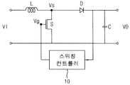
도 2는 도 1의 스위칭 컨트롤러를 나타내는 회로도이다.
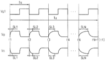
도 3은 도 1의 DC-DC 컨버터의 입출력 신호를 나타내는 타이밍도이다.
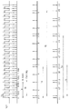
도 4는 도 2의 스위치 게이트 구동부의 입력 전압의 주기 및 슬루율 제어부의 슬루율 변화 주기를 나타내는 타이밍도이다.
도 5는 본 발명의 다른 실시예에 따른 DC-DC 컨버터의 입출력 신호를 나타내는 타이밍도이다.
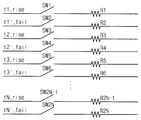
도 6은 본 발명의 다른 실시예에 따른 스위칭 컨트롤러의 슬루율 제어부를 나타내는 회로도이다.
도 7은 도 6의 스위칭 컨트롤러의 스위치 게이트 구동부의 입력 전압의 주기 및 슬루율 제어부의 슬루율 변화 주기를 나타내는 타이밍도이다.
도 8은 본 발명의 다른 실시예에 따른 DC-DC 컨버터의 스위칭 컨트롤러를 나타내는 회로도이다.
도 9는 도 8의 DC-DC 컨버터의 입출력 신호를 나타내는 타이밍도이다.
도 10은 본 발명의 다른 실시예에 따른 DC-DC 컨버터의 입출력 신호를 나타내는 타이밍도이다.
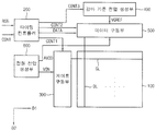
도 11은 본 발명의 다른 실시예에 따른 표시 장치를 나타내는 블록도이다.
14, 14A: 슬루율 제어부 141: 컨트롤부
142: 디지털-아날로그 컨버터 100: 표시 패널
200: 타이밍 컨트롤러 300: 게이트 구동부
400: 감마 기준 전압 생성부 500: 데이터 구동부
600: 전원 전압 생성부
Claims (20)
- 턴 온 및 턴 오프를 반복하여 입력 DC 전압을 기초로 출력 DC 전압을 생성하는 파워 스위치; 및
상기 파워 스위치의 동작을 제어하는 스위칭 컨트롤러를 포함하고,
상기 스위칭 컨트롤러는 상기 파워 스위치의 일단의 스위치 전압의 슬루율을 시간에 따라 가변시키는 슬루율 제어부를 포함하는 것을 특징으로 하는 DC-DC 컨버터. - 제1항에 있어서, 상기 스위칭 컨트롤러는 제1 주기를 갖는 제1 전압의 레벨을 조절하여 상기 제1 주기를 갖는 제2 전압을 생성하는 스위치 게이트 구동부를 더 포함하는 것을 특징으로 하는 DC-DC 컨버터.
- 제2항에 있어서, 상기 슬루율 제어부는 병렬로 연결되는 N개의 저항들을 포함하고,
상기 N개의 저항들은 상기 N개의 저항들에 직렬로 연결되는 N개의 스위치들에 의해 상기 파워 스위치와 상기 스위치 게이트 구동부를 교대로 연결하는 것을 특징으로 하는 DC-DC 컨버터. - 제3항에 있어서, 상기 N개의 저항들은 서로 다른 저항 값을 갖는 것을 특징으로 하는 DC-DC 컨버터.
- 제4항에 있어서, 상기 파워 스위치와 상기 스위치 게이트 구동부를 연결하는 상기 슬루율 제어부의 저항 값이 클수록 상기 스위치 전압의 슬루율이 낮아지는 것을 특징으로 하는 DC-DC 컨버터.
- 제3항에 있어서, 상기 슬루율 제어부의 제1 스위치 내지 제N 스위치는 순차적으로 턴 온 되고,
상기 제N 스위치가 턴 온 된 후 상기 제1 스위치가 턴 온 되며,
상기 제1 스위치가 턴 온 되고, 다시 상기 제1 스위치가 턴 온 될 때까지의 시간으로 정의되는 슬루율 변화 주기는 상기 제1 주기의 N배인 것을 특징으로 하는 DC-DC 컨버터. - 제3항에 있어서, 상기 슬루율 제어부의 제1 스위치 내지 제N 스위치는 순차적으로 턴 온 되고,
상기 제N 스위치가 턴 온 된 후 제N-1 스위치 내지 상기 제1 스위치가 순차적으로 턴 온 되며,
상기 제1 스위치가 턴 온 되고, 다시 상기 제1 스위치가 턴 온 될 때까지의 시간으로 정의되는 슬루율 변화 주기는 상기 제1 주기의 2N-2배인 것을 특징으로 하는 DC-DC 컨버터. - 제3항에 있어서, 상기 슬루율 제어부의 제1 스위치는 상기 제1 전압의 제1 펄스의 라이징 에지에 대응하여 턴 온 되고, 상기 슬루율 제어부의 제2 스위치는 상기 제1 전압의 제2 펄스의 라이징 에지에 대응하여 턴 온 되는 것을 특징으로 하는 DC-DC 컨버터.
- 제3항에 있어서, 상기 슬루율 제어부의 제1 스위치는 상기 제1 전압의 제1 펄스의 라이징 에지에 대응하여 턴 온 되고, 상기 슬루율 제어부의 제2 스위치는 상기 제1 전압의 상기 제1 펄스의 폴링 에지에 대응하여 턴 온 되는 것을 특징으로 하는 DC-DC 컨버터.
- 제9항에 있어서, 상기 제1 전압의 펄스들의 라이징 에지에 대응하여 순차적으로 턴 온 되는 제1 스위치 그룹의 반복 주기는 상기 제1 전압의 상기 펄스들의 폴링 에지에 대응하여 순차적으로 턴 온 되는 제2 스위치 그룹의 반복 주기와 상이한 것을 특징으로 하는 DC-DC 컨버터.
- 제3항에 있어서, 상기 스위치 게이트 구동부는 제1 스위칭 소자, 제2 스위칭 소자 및 제3 스위칭 소자를 포함하고,
상기 제1 스위칭 소자는 상기 제1 전압이 인가되는 제어 전극, 하이 레벨의 제1 DC 전압이 인가되는 입력 전극 및 로우 레벨의 제2 DC 전압이 인가되는 출력 전극을 포함하고,
상기 제2 스위칭 소자는 상기 제1 스위칭 소자의 상기 입력 전극에 연결되는 제어 전극, 상기 제1 DC 전압이 인가되는 입력 전극 및 상기 제3 스위칭 소자의 입력 전극에 연결되는 출력 전극을 포함하며,
상기 제3 스위칭 소자는 상기 제1 스위칭 소자의 상기 입력 전극에 연결되는 제어 전극, 상기 제2 스위칭 소자의 상기 출력 전극에 연결되는 입력 전극 및 상기 제2 DC 전압이 인가되는 출력 전극을 포함하는 것을 특징으로 하는 DC-DC 컨버터. - 제2항에 있어서, 상기 슬루율 제어부는 입력 신호에 따라 서로 다른 레벨을 갖는 가변 전원 전압을 생성하는 것을 특징으로 하는 DC-DC 컨버터.
- 제12항에 있어서, 상기 슬루율 제어부는
상기 입력 신호를 수신하여 입력 아날로그 신호를 생성하는 디지털-아날로그 컨버터;
상기 디지털-아날로그 컨버터에 연결되는 증폭기; 및
상기 증폭기에 연결되는 제4 스위칭 소자를 포함하는 것을 특징으로 하는 DC-DC 컨버터. - 제12항에 있어서, 상기 가변 전원 전압의 레벨이 클수록 상기 스위치 전압의 슬루율이 높아지는 것을 특징으로 하는 DC-DC 컨버터.
- 제12항에 있어서, 상기 가변 전원 전압의 레벨은 제1 레벨로부터 제N 레벨까지 순차적으로 감소하고,
상기 가변 전원 전압이 상기 제N 레벨에 도달한 후 상기 제1 레벨로 증가하며,
상기 가변 전원 전압이 상기 제1 레벨로부터 상기 제N 레벨까지 감소하였다가 다시 상기 제1 레벨로 돌아올 때까지의 시간으로 정의되는 슬루율 변화 주기는 상기 제1 주기의 N배인 것을 특징으로 하는 DC-DC 컨버터. - 제12항에 있어서, 상기 가변 전원 전압의 레벨은 제1 레벨로부터 제N 레벨까지 순차적으로 감소하고,
상기 가변 전원 전압이 상기 제N 레벨에 도달한 후 제N-1 레벨로부터 상기 제1 레벨까지 순차적으로 증가하며,
상기 가변 전원 전압이 상기 제1 레벨로부터 상기 제N 레벨까지 감소하였다가 다시 상기 제1 레벨로 돌아올 때까지의 시간으로 정의되는 슬루율 변화 주기는 상기 제1 주기의 2N-2배인 것을 특징으로 하는 DC-DC 컨버터. - 제12항에 있어서, 상기 스위치 게이트 구동부는 제1 스위칭 소자, 제2 스위칭 소자 및 제3 스위칭 소자를 포함하고,
상기 제1 스위칭 소자는 상기 제1 전압이 인가되는 제어 전극, 상기 가변 전원 전압이 인가되는 입력 전극 및 로우 레벨의 제2 DC 전압이 인가되는 출력 전극을 포함하고,
상기 제2 스위칭 소자는 상기 제1 스위칭 소자의 상기 입력 전극에 연결되는 제어 전극, 하이 레벨의 제1 DC 전압이 인가되는 입력 전극 및 상기 제3 스위칭 소자의 입력 전극에 연결되는 출력 전극을 포함하며,
상기 제3 스위칭 소자는 상기 제1 스위칭 소자의 상기 입력 전극에 연결되는 제어 전극, 상기 제2 스위칭 소자의 상기 출력 전극에 연결되는 입력 전극 및 상기 제2 DC 전압이 인가되는 출력 전극을 포함하는 것을 특징으로 하는 DC-DC 컨버터. - 영상을 표시하는 표시 패널;
턴 온 및 턴 오프를 반복하여 입력 DC 전압을 기초로 출력 DC 전압을 생성하는 파워 스위치 및 상기 파워 스위치의 동작을 제어하는 스위칭 컨트롤러를 포함하는 DC-DC 컨버터; 및
상기 출력 DC 전압을 기초로 상기 표시 패널을 구동하는 표시 패널 구동부를 포함하고,
상기 스위칭 컨트롤러는 상기 파워 스위치의 일단의 스위치 전압의 슬루율을 시간에 따라 가변시키는 슬루율 제어부를 포함하는 것을 특징으로 하는 표시 장치. - 제18항에 있어서, 상기 표시 패널 구동부는 상기 표시 패널의 게이트 라인에 게이트 신호를 출력하는 게이트 구동부를 포함하고,
상기 DC-DC 컨버터의 상기 출력 DC 전압은 상기 게이트 신호의 하이 레벨을 정의하는 게이트 온 전압인 것을 특징으로 하는 표시 장치. - 제18항에 있어서, 상기 표시 패널 구동부는 상기 표시 패널의 데이터 라인에 데이터 전압을 출력하는 데이터 구동부를 포함하고,
상기 DC-DC 컨버터의 상기 출력 DC 전압은 상기 데이터 전압을 생성하기 위한 아날로그 하이 전원 전압인 것을 특징으로 하는 표시 장치.
Priority Applications (3)
| Application Number | Priority Date | Filing Date | Title |
|---|---|---|---|
| KR1020140144511A KR102240284B1 (ko) | 2014-10-23 | 2014-10-23 | Dc-dc 컨버터 및 이를 포함하는 표시 장치 |
| CN201510688237.8A CN105553270B (zh) | 2014-10-23 | 2015-10-21 | Dc-dc转换器以及具有dc-dc转换器的显示装置 |
| US14/920,176 US10083671B2 (en) | 2014-10-23 | 2015-10-22 | DC-DC converter and display apparatus having the same |
Applications Claiming Priority (1)
| Application Number | Priority Date | Filing Date | Title |
|---|---|---|---|
| KR1020140144511A KR102240284B1 (ko) | 2014-10-23 | 2014-10-23 | Dc-dc 컨버터 및 이를 포함하는 표시 장치 |
Publications (2)
| Publication Number | Publication Date |
|---|---|
| KR20160048314A true KR20160048314A (ko) | 2016-05-04 |
| KR102240284B1 KR102240284B1 (ko) | 2021-04-15 |
Family
ID=55792780
Family Applications (1)
| Application Number | Title | Priority Date | Filing Date |
|---|---|---|---|
| KR1020140144511A Active KR102240284B1 (ko) | 2014-10-23 | 2014-10-23 | Dc-dc 컨버터 및 이를 포함하는 표시 장치 |
Country Status (3)
| Country | Link |
|---|---|
| US (1) | US10083671B2 (ko) |
| KR (1) | KR102240284B1 (ko) |
| CN (1) | CN105553270B (ko) |
Cited By (3)
| Publication number | Priority date | Publication date | Assignee | Title |
|---|---|---|---|---|
| KR20190065725A (ko) * | 2017-12-04 | 2019-06-12 | 엘지전자 주식회사 | 컨버터 및 그를 포함하는 전력변환장치 |
| US10522070B2 (en) | 2016-11-03 | 2019-12-31 | Samsung Display Co., Ltd. | Converter and display apparatus including the same |
| US12205518B2 (en) | 2022-11-30 | 2025-01-21 | Samsung Display Co., Ltd. | Power voltage generator, driver IC, and display device |
Families Citing this family (3)
| Publication number | Priority date | Publication date | Assignee | Title |
|---|---|---|---|---|
| KR102450738B1 (ko) * | 2017-11-20 | 2022-10-05 | 삼성전자주식회사 | 소스 구동 회로 및 이를 포함하는 디스플레이 장치 |
| US10840795B1 (en) * | 2019-10-16 | 2020-11-17 | Monolithic Power Systems, Inc. | Power transistor driver with reduced spikes for switching converters |
| CN113470590A (zh) * | 2021-07-15 | 2021-10-01 | Tcl华星光电技术有限公司 | 逻辑电路和显示面板 |
Citations (4)
| Publication number | Priority date | Publication date | Assignee | Title |
|---|---|---|---|---|
| JP2011078193A (ja) * | 2009-09-30 | 2011-04-14 | Sharp Corp | 映像表示装置 |
| JP2011091923A (ja) * | 2009-10-21 | 2011-05-06 | Mitsubishi Electric Corp | 電圧駆動型スイッチングデバイスの駆動回路 |
| JP2012129971A (ja) * | 2010-11-22 | 2012-07-05 | Denso Corp | 負荷駆動装置 |
| JP2014011830A (ja) * | 2012-06-28 | 2014-01-20 | Hitachi Appliances Inc | 電力変換装置 |
Family Cites Families (19)
| Publication number | Priority date | Publication date | Assignee | Title |
|---|---|---|---|---|
| US5636114A (en) | 1995-11-30 | 1997-06-03 | Electronic Measurements, Inc. | Lossless snubber circuit for use in power converters |
| US6335638B1 (en) | 2000-06-29 | 2002-01-01 | Pericom Semiconductor Corp. | Triple-slope clock driver for reduced EMI |
| US6434029B1 (en) | 2001-10-17 | 2002-08-13 | Astec International Limited | Boost topology having an auxiliary winding on the snubber inductor |
| TW556401B (en) | 2002-02-01 | 2003-10-01 | Potrans Electrical Corp | Converter using synchronous rectification circuit and associated with LC snubber apparatus |
| JP2005165604A (ja) | 2003-12-02 | 2005-06-23 | Seiko Instruments Inc | オーバーシュート回復回路及び電圧レギュレータ |
| US7190225B2 (en) | 2004-09-23 | 2007-03-13 | Maxim Integrated Products, Inc. | Efficient low EMI switching output stages and methods |
| US7777461B2 (en) * | 2005-10-31 | 2010-08-17 | Chil Semiconductor Corporation | Power supply and controller circuits |
| US7489117B2 (en) * | 2005-10-31 | 2009-02-10 | Chil Semiconductor Corporation | Dynamic conversion circuit for a voltage regulator module |
| US7852053B2 (en) * | 2005-10-31 | 2010-12-14 | Chil Semiconductor Corporation | Power supply and controller circuits |
| US7456618B2 (en) * | 2005-10-31 | 2008-11-25 | Chil Semiconductor, Inc. | Digital controller for a voltage regulator module |
| US7592789B2 (en) * | 2005-10-31 | 2009-09-22 | Chil Semiconductor Corporation | Power supply and related circuits |
| US8723438B2 (en) | 2007-03-12 | 2014-05-13 | Cirrus Logic, Inc. | Switch power converter control with spread spectrum based electromagnetic interference reduction |
| US8035364B2 (en) | 2007-04-25 | 2011-10-11 | Advanced Analogic Technologies, Inc. | Step-down switching regulator with freewheeling diode |
| US7923974B2 (en) * | 2008-01-04 | 2011-04-12 | Chil Semiconductor Corporation | Modification of switch activation order in a power supply |
| CN102906980B (zh) | 2010-05-21 | 2015-08-19 | 株式会社半导体能源研究所 | 半导体装置及显示装置 |
| US9093903B2 (en) * | 2011-09-28 | 2015-07-28 | Monolithic Power Systems, Inc. | Power converter with voltage window and the method thereof |
| JP2013150453A (ja) | 2012-01-19 | 2013-08-01 | Renesas Electronics Corp | コントーラ |
| KR101989575B1 (ko) * | 2012-12-07 | 2019-06-14 | 삼성전자주식회사 | 스위칭 전압 스파이크를 적응적으로 제어하는 어댑티브 전원 컨버팅 장치 |
| JP6231314B2 (ja) * | 2013-07-16 | 2017-11-15 | シナプティクス・ジャパン合同会社 | 表示駆動装置 |
-
2014
- 2014-10-23 KR KR1020140144511A patent/KR102240284B1/ko active Active
-
2015
- 2015-10-21 CN CN201510688237.8A patent/CN105553270B/zh active Active
- 2015-10-22 US US14/920,176 patent/US10083671B2/en active Active
Patent Citations (4)
| Publication number | Priority date | Publication date | Assignee | Title |
|---|---|---|---|---|
| JP2011078193A (ja) * | 2009-09-30 | 2011-04-14 | Sharp Corp | 映像表示装置 |
| JP2011091923A (ja) * | 2009-10-21 | 2011-05-06 | Mitsubishi Electric Corp | 電圧駆動型スイッチングデバイスの駆動回路 |
| JP2012129971A (ja) * | 2010-11-22 | 2012-07-05 | Denso Corp | 負荷駆動装置 |
| JP2014011830A (ja) * | 2012-06-28 | 2014-01-20 | Hitachi Appliances Inc | 電力変換装置 |
Cited By (4)
| Publication number | Priority date | Publication date | Assignee | Title |
|---|---|---|---|---|
| US10522070B2 (en) | 2016-11-03 | 2019-12-31 | Samsung Display Co., Ltd. | Converter and display apparatus including the same |
| US10796624B2 (en) | 2016-11-03 | 2020-10-06 | Samsung Display Co., Ltd. | Converter and display apparatus including the same |
| KR20190065725A (ko) * | 2017-12-04 | 2019-06-12 | 엘지전자 주식회사 | 컨버터 및 그를 포함하는 전력변환장치 |
| US12205518B2 (en) | 2022-11-30 | 2025-01-21 | Samsung Display Co., Ltd. | Power voltage generator, driver IC, and display device |
Also Published As
| Publication number | Publication date |
|---|---|
| US20160118875A1 (en) | 2016-04-28 |
| KR102240284B1 (ko) | 2021-04-15 |
| CN105553270A (zh) | 2016-05-04 |
| US10083671B2 (en) | 2018-09-25 |
| CN105553270B (zh) | 2019-10-15 |
Similar Documents
| Publication | Publication Date | Title |
|---|---|---|
| CN102111071B (zh) | Dc-dc转换器及其控制方法以及使用它们的显示装置 | |
| KR102240284B1 (ko) | Dc-dc 컨버터 및 이를 포함하는 표시 장치 | |
| CN106257580B (zh) | 显示设备和驱动该显示设备的方法 | |
| EP2393191B1 (en) | Boost converter for liquid crystal display | |
| US9143148B2 (en) | Amplification circuit, source driver, electrooptical device, and electronic device | |
| JP2018519539A (ja) | 表示パネル用の発光制御装置及び方法 | |
| JP2009271530A (ja) | ソースドライバー及びそれを含むディスプレイ装置 | |
| JP2013246431A (ja) | 表示装置及びその駆動方法 | |
| US20110102406A1 (en) | Gate driver and operating method thereof | |
| KR102554201B1 (ko) | 디스플레이 드라이버 ic 및 이를 포함하는 디스플레이 장치 | |
| US10770022B2 (en) | Source driver and a display driver integrated circuit | |
| CN113422510A (zh) | Dc-dc转换器 | |
| JP2009300866A (ja) | 駆動回路および表示装置 | |
| TWI488170B (zh) | Display the drive circuit of the panel | |
| US8253667B2 (en) | Display control device and method of controlling same | |
| KR102182052B1 (ko) | 유기발광표시장치 | |
| WO2016011678A1 (zh) | 数字模拟转换器、可编程伽玛校正缓冲电路及显示装置 | |
| KR20090105148A (ko) | 표시 장치 | |
| KR102534116B1 (ko) | Dc-dc 컨버터, 이를 포함하는 표시 장치 | |
| KR102023932B1 (ko) | 전원 공급부 및 이를 이용한 평판 표시 장치 | |
| JP7544624B2 (ja) | 出力回路、表示ドライバ及び表示装置 | |
| KR20150088598A (ko) | 데이터 구동부, 이를 구비하는 표시 장치 및 이를 이용하는 표시 패널의 구동 방법 | |
| US20050052401A1 (en) | Display apparatus, device for driving the display apparatus, and method of driving the display apparatus | |
| KR20160083577A (ko) | 표시장치 | |
| JP2009251046A (ja) | 画像表示装置およびその制御方法 |
Legal Events
| Date | Code | Title | Description |
|---|---|---|---|
| PA0109 | Patent application |
St.27 status event code: A-0-1-A10-A12-nap-PA0109 |
|
| R18-X000 | Changes to party contact information recorded |
St.27 status event code: A-3-3-R10-R18-oth-X000 |
|
| PG1501 | Laying open of application |
St.27 status event code: A-1-1-Q10-Q12-nap-PG1501 |
|
| R18-X000 | Changes to party contact information recorded |
St.27 status event code: A-3-3-R10-R18-oth-X000 |
|
| A201 | Request for examination | ||
| PA0201 | Request for examination |
St.27 status event code: A-1-2-D10-D11-exm-PA0201 |
|
| D13-X000 | Search requested |
St.27 status event code: A-1-2-D10-D13-srh-X000 |
|
| D14-X000 | Search report completed |
St.27 status event code: A-1-2-D10-D14-srh-X000 |
|
| E902 | Notification of reason for refusal | ||
| PE0902 | Notice of grounds for rejection |
St.27 status event code: A-1-2-D10-D21-exm-PE0902 |
|
| P11-X000 | Amendment of application requested |
St.27 status event code: A-2-2-P10-P11-nap-X000 |
|
| P13-X000 | Application amended |
St.27 status event code: A-2-2-P10-P13-nap-X000 |
|
| E701 | Decision to grant or registration of patent right | ||
| PE0701 | Decision of registration |
St.27 status event code: A-1-2-D10-D22-exm-PE0701 |
|
| GRNT | Written decision to grant | ||
| PR0701 | Registration of establishment |
St.27 status event code: A-2-4-F10-F11-exm-PR0701 |
|
| PR1002 | Payment of registration fee |
St.27 status event code: A-2-2-U10-U11-oth-PR1002 Fee payment year number: 1 |
|
| PG1601 | Publication of registration |
St.27 status event code: A-4-4-Q10-Q13-nap-PG1601 |
|
| PR1001 | Payment of annual fee |
St.27 status event code: A-4-4-U10-U11-oth-PR1001 Fee payment year number: 4 |
|
| PR1001 | Payment of annual fee |
St.27 status event code: A-4-4-U10-U11-oth-PR1001 Fee payment year number: 5 |
|
| PR1001 | Payment of annual fee |
St.27 status event code: A-4-4-U10-U11-oth-PR1001 Fee payment year number: 6 |
|
| U11 | Full renewal or maintenance fee paid |
Free format text: ST27 STATUS EVENT CODE: A-4-4-U10-U11-OTH-PR1001 (AS PROVIDED BY THE NATIONAL OFFICE) Year of fee payment: 6 |