KR20160051644A - Xrf를 사용한 작은 특징부의 측정 - Google Patents
Xrf를 사용한 작은 특징부의 측정 Download PDFInfo
- Publication number
- KR20160051644A KR20160051644A KR1020150150868A KR20150150868A KR20160051644A KR 20160051644 A KR20160051644 A KR 20160051644A KR 1020150150868 A KR1020150150868 A KR 1020150150868A KR 20150150868 A KR20150150868 A KR 20150150868A KR 20160051644 A KR20160051644 A KR 20160051644A
- Authority
- KR
- South Korea
- Prior art keywords
- ray
- xrf
- feature
- interest
- beam profile
- Prior art date
- Legal status (The legal status is an assumption and is not a legal conclusion. Google has not performed a legal analysis and makes no representation as to the accuracy of the status listed.)
- Granted
Links
- 238000005259 measurement Methods 0.000 title claims description 25
- 238000004876 x-ray fluorescence Methods 0.000 claims abstract description 99
- 238000007689 inspection Methods 0.000 claims abstract description 28
- 230000004044 response Effects 0.000 claims abstract description 26
- 238000012360 testing method Methods 0.000 claims abstract description 20
- 238000000691 measurement method Methods 0.000 claims abstract 2
- 238000000034 method Methods 0.000 claims description 49
- 235000012431 wafers Nutrition 0.000 claims description 33
- 238000012937 correction Methods 0.000 claims description 25
- 239000004065 semiconductor Substances 0.000 claims description 19
- 230000007613 environmental effect Effects 0.000 claims description 9
- 229910052751 metal Inorganic materials 0.000 claims description 7
- 239000002184 metal Substances 0.000 claims description 7
- 238000004364 calculation method Methods 0.000 claims description 2
- 230000005855 radiation Effects 0.000 abstract 1
- 230000006870 function Effects 0.000 description 11
- 238000004458 analytical method Methods 0.000 description 9
- 238000010586 diagram Methods 0.000 description 7
- 230000005284 excitation Effects 0.000 description 7
- 239000000463 material Substances 0.000 description 7
- 238000003858 X-ray microfluorescence spectroscopy Methods 0.000 description 5
- 238000001228 spectrum Methods 0.000 description 5
- 238000009681 x-ray fluorescence measurement Methods 0.000 description 5
- 230000008859 change Effects 0.000 description 4
- 238000004519 manufacturing process Methods 0.000 description 4
- 230000004048 modification Effects 0.000 description 4
- 238000012986 modification Methods 0.000 description 4
- 230000003287 optical effect Effects 0.000 description 4
- 238000001514 detection method Methods 0.000 description 3
- 230000008439 repair process Effects 0.000 description 3
- 238000004846 x-ray emission Methods 0.000 description 3
- XUIMIQQOPSSXEZ-UHFFFAOYSA-N Silicon Chemical compound [Si] XUIMIQQOPSSXEZ-UHFFFAOYSA-N 0.000 description 2
- 238000009795 derivation Methods 0.000 description 2
- 230000001678 irradiating effect Effects 0.000 description 2
- 230000002093 peripheral effect Effects 0.000 description 2
- 230000008569 process Effects 0.000 description 2
- 238000012545 processing Methods 0.000 description 2
- 229910052710 silicon Inorganic materials 0.000 description 2
- 239000010703 silicon Substances 0.000 description 2
- 230000003595 spectral effect Effects 0.000 description 2
- WHXSMMKQMYFTQS-UHFFFAOYSA-N Lithium Chemical compound [Li] WHXSMMKQMYFTQS-UHFFFAOYSA-N 0.000 description 1
- 238000012951 Remeasurement Methods 0.000 description 1
- 238000012512 characterization method Methods 0.000 description 1
- 230000007423 decrease Effects 0.000 description 1
- 230000008021 deposition Effects 0.000 description 1
- 230000001066 destructive effect Effects 0.000 description 1
- 238000011156 evaluation Methods 0.000 description 1
- 230000004907 flux Effects 0.000 description 1
- 229910052744 lithium Inorganic materials 0.000 description 1
- 230000007246 mechanism Effects 0.000 description 1
- 238000004445 quantitative analysis Methods 0.000 description 1
Images


Classifications
-
- G—PHYSICS
- G01—MEASURING; TESTING
- G01N—INVESTIGATING OR ANALYSING MATERIALS BY DETERMINING THEIR CHEMICAL OR PHYSICAL PROPERTIES
- G01N23/00—Investigating or analysing materials by the use of wave or particle radiation, e.g. X-rays or neutrons, not covered by groups G01N3/00 – G01N17/00, G01N21/00 or G01N22/00
- G01N23/22—Investigating or analysing materials by the use of wave or particle radiation, e.g. X-rays or neutrons, not covered by groups G01N3/00 – G01N17/00, G01N21/00 or G01N22/00 by measuring secondary emission from the material
- G01N23/223—Investigating or analysing materials by the use of wave or particle radiation, e.g. X-rays or neutrons, not covered by groups G01N3/00 – G01N17/00, G01N21/00 or G01N22/00 by measuring secondary emission from the material by irradiating the sample with X-rays or gamma-rays and by measuring X-ray fluorescence
-
- G—PHYSICS
- G01—MEASURING; TESTING
- G01B—MEASURING LENGTH, THICKNESS OR SIMILAR LINEAR DIMENSIONS; MEASURING ANGLES; MEASURING AREAS; MEASURING IRREGULARITIES OF SURFACES OR CONTOURS
- G01B15/00—Measuring arrangements characterised by the use of electromagnetic waves or particle radiation, e.g. by the use of microwaves, X-rays, gamma rays or electrons
- G01B15/02—Measuring arrangements characterised by the use of electromagnetic waves or particle radiation, e.g. by the use of microwaves, X-rays, gamma rays or electrons for measuring thickness
-
- G—PHYSICS
- G01—MEASURING; TESTING
- G01N—INVESTIGATING OR ANALYSING MATERIALS BY DETERMINING THEIR CHEMICAL OR PHYSICAL PROPERTIES
- G01N2223/00—Investigating materials by wave or particle radiation
- G01N2223/07—Investigating materials by wave or particle radiation secondary emission
- G01N2223/076—X-ray fluorescence
-
- G—PHYSICS
- G01—MEASURING; TESTING
- G01N—INVESTIGATING OR ANALYSING MATERIALS BY DETERMINING THEIR CHEMICAL OR PHYSICAL PROPERTIES
- G01N2223/00—Investigating materials by wave or particle radiation
- G01N2223/10—Different kinds of radiation or particles
- G01N2223/101—Different kinds of radiation or particles electromagnetic radiation
- G01N2223/1016—X-ray
-
- G—PHYSICS
- G01—MEASURING; TESTING
- G01N—INVESTIGATING OR ANALYSING MATERIALS BY DETERMINING THEIR CHEMICAL OR PHYSICAL PROPERTIES
- G01N2223/00—Investigating materials by wave or particle radiation
- G01N2223/30—Accessories, mechanical or electrical features
- G01N2223/303—Accessories, mechanical or electrical features calibrating, standardising
-
- G—PHYSICS
- G01—MEASURING; TESTING
- G01N—INVESTIGATING OR ANALYSING MATERIALS BY DETERMINING THEIR CHEMICAL OR PHYSICAL PROPERTIES
- G01N2223/00—Investigating materials by wave or particle radiation
- G01N2223/30—Accessories, mechanical or electrical features
- G01N2223/323—Accessories, mechanical or electrical features irradiation range monitor, e.g. light beam
-
- G—PHYSICS
- G01—MEASURING; TESTING
- G01N—INVESTIGATING OR ANALYSING MATERIALS BY DETERMINING THEIR CHEMICAL OR PHYSICAL PROPERTIES
- G01N2223/00—Investigating materials by wave or particle radiation
- G01N2223/60—Specific applications or type of materials
- G01N2223/611—Specific applications or type of materials patterned objects; electronic devices
- G01N2223/6116—Specific applications or type of materials patterned objects; electronic devices semiconductor wafer
Landscapes
- Physics & Mathematics (AREA)
- General Physics & Mathematics (AREA)
- Electromagnetism (AREA)
- Health & Medical Sciences (AREA)
- Life Sciences & Earth Sciences (AREA)
- Chemical & Material Sciences (AREA)
- Analytical Chemistry (AREA)
- Biochemistry (AREA)
- General Health & Medical Sciences (AREA)
- Immunology (AREA)
- Pathology (AREA)
- Analysing Materials By The Use Of Radiation (AREA)
Abstract
Description
도 2는 본 발명의 실시예에 따른, 웨이퍼 상의 관심의 패드(POI) 위의 엑스선 빔의 파라미터를 도시하는 반도체 웨이퍼 위의 영역의 개략 평면도이다.
도 3은 본 발명의 실시예에 따른, 웨이퍼 상의 POI 위의 스캔 동안 여기 엑스선 빔의 위치의 함수로서의 엑스선 형광(XRF) 강도의 개략도이다.
도 4는 본 발명의 실시예에 따른, 엑스선 빔 크기를 교정하기 위한 방법을 개략적으로 도시하는 순서도이다.
도 5는 본 발명의 실시예에 따른, XRF 측정의 분석에 사용되는 상대 방출 계수를 계산하기 위한 방법을 개략적으로 도시하는 순서도이다.
도 6은 본 발명의 실시예에 따른, 시료 상의 특징부의 XRF 측정 및 분석을 위한 방법을 개략적으로 도시하는 순서도이다.
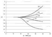
도 7은 본 발명의 실시예에 따른, 다양한 상이한 검사 조건에 대해 계산되는 환경적 보정 계수를 개략적으로 도시하는 도면이다.




Claims (20)
- 엑스선 측정 방법으로서,
교정 시기에서, 제1 빔 프로필을 갖는 제1 엑스선 빔을 교정 시료 위의 관심의 특징부를 가로질러 스캔하고, 상기 제1 엑스선 빔에 응답하여, 상기 특징부로부터 그리고 상기 특징부를 둘러싸는 상기 교정 시료의 배경 에어리어로부터 방출되는 제1 엑스선 형광(XRF)을 측정하는 단계;
상기 제1 XRF 및 상기 제1 빔 프로필에 응답하여, 상기 특징부와 상기 특징부를 둘러싸는 배경 에어리어 사이의 XRF 방출 강도의 관계를 나타내는 상대 방출 계수를 계산하는 단계;
검사 시기에서, 검사 시료 위의 상기 관심의 특징부에 조사시키기 위해, 상기 제1 빔 프로필과 상이한 제2 빔 프로필을 갖는 제2 엑스선 빔을 지향시키고, 상기 제2 엑스선 빔에 응답하여 상기 검사 시료로부터 방출된 제2 XRF를 측정하는 단계; 및
상기 제2 빔 프로필과 함께 상기 상대 방출 계수를 상기 측정된 제2 XRF에 적용함으로써 상기 검사 시료 위의 관심의 특징부의 특성을 계산하는 단계를 포함하는 것을 특징으로 하는 엑스선 측정 방법. - 제1항에 있어서, 상기 계산된 특성은 상기 특징부의 조성 및 두께로 구성된 특성의 그룹으로부터 선택되는 것을 특징으로 하는 엑스선 측정 방법.
- 제2항에 있어서, 상기 계산하는 단계는,
상기 상대 방출 계수 및 상기 제2 빔 프로필에 기초하여 환경 보정 계수를 계산하는 단계;
상기 환경 보정 계수에 의해 상기 제2 XRF의 측정 강도를 스케일링함으로써 상기 제2 XRF의 보정 강도를 계산하는 단계; 및
계산된 조성 또는 두께를 상기 보정 강도로부터 유도하는 단계를 포함하는 것을 특징으로 하는 엑스선 측정 방법. - 제3항에 있어서, 상기 환경 보정 계수는 상기 검사 시료 위의 관심의 특징부를 둘러싸는 배경 에어리어에 입사되는 제2 엑스선 빔의 일부에 의존하고 상기 제2 엑스선 빔의 일부를 보상하는 것을 특징으로 하는 엑스선 측정 방법.
- 제1항에 있어서, 상기 상대 방출 계수를 계산하는 단계는 상이한, 각각의 XRF 에너지에서, 상기 관심의 특징부 내의 복수의 상이한 요소에 대해, 제1 XRF를 측정하고 상이한, 각각의 상대 방출 계수를 계산하는 단계를 포함하고,
상기 특성을 계산하는 단계는 상기 측정된 제2 XRF의 에너지에 의존하여 적용할 상기 각각의 상대 방출 계수의 하나 이상을 선택하는 단계를 포함하는 것을 특징으로 하는 엑스선 측정 방법. - 제1항 내지 제5항중 어느 한 항에 있어서, 상기 교정 시기에서, 상기 제1 빔 프로필을 측정하는 단계를 포함하는 것을 특징으로 하는 엑스선 측정 방법.
- 제6항에 있어서, 상기 제1 빔 프로필을 측정하는 단계는 상기 제1 엑스선 빔의 복수의 상이한 에너지에서 제1 빔의 폭을 측정하는 단계, 상기 폭의 에너지 의존도를 찾는 단계를 포함하고, 상기 상대 방출 계수를 계산하는 단계는, 상기 에너지 의존도에 기초하여, 특정 에너지에서 상기 제1 빔의 폭을 추정하는 단계, 및 상기 상대 방출 계수를 찾을 때 상기 추정된 폭을 적용하는 단계를 포함하는 것을 특징으로 하는 엑스선 측정 방법.
- 제7항에 있어서, 상기 제1 빔 프로필을 측정하는 단계는 상기 상이한 에너지의 각각에서, 상기 제1 엑스선 빔을 타겟의 에지를 가로질러 스캔하는 단계, 및 상기 제1 엑스선 빔을 스캔하는 동안 상기 타겟으로부터의 XRF의 강도를 측정하는 단계를 포함하는 것을 특징으로 하는 엑스선 측정 방법.
- 제6항에 있어서, 상기 검사 시기에서, 상기 제2 빔 프로필을 측정하는 단계를 포함하고, 상기 특성을 계산하는 단계는 상기 특성을 계산할 때 상기 상대 방출 계수와 함께, 상기 측정된 제2 빔 프로필을 적용하는 단계를 포함하는 것을 특징으로 하는 엑스선 측정 방법.
- 제1항 내지 제5항중 어느 한 항에 있어서, 상기 교정 및 검사 시료는 반도체 웨이퍼를 포함하고, 상기 관심의 특징부는 상기 반도체 웨이퍼의 각각 위의 사전규정된 위치에 형성된 금속 패드를 포함하고, 상기 배경 에어리어는 상기 사전규정된 위치 둘레의 반도체 웨이퍼 위에 형성된 다른 구조를 포함하는 것을 특징으로 하는 엑스선 측정 방법.
- 엑스선 측정 장치에 있어서,
시료에 조사하기 위해 엑스선 빔을 지향시키도록 구성된 엑스선 빔 소스;
상기 엑스선 빔에 응답하여 상기 시료로부터 방출된 엑스선 형광(XRF)을 감지하도록 구성된 엑스선 검출기;
상기 엑스선 빔이 상기 시료를 가로질러 스캔하도록 구성된 모션 어셈블리; 및
상기 엑스선 빔 소스 및 상기 모션 어셈블리를 제어하고 교정 시기 및 검사 시기에 상기 방출된 XRF에 응답하여 상기 엑스선 검출기로부터 신호를 수신하도록 구성된 프로세서를 포함하고,
상기 교정 시기에, 상기 모션 어셈블리는 제1 빔 프로필을 갖는 제1 엑스선 빔을 교정 시료 위의 관심의 특징부를 가로질러 스캔하고, 상기 프로세서는 상기 제1 엑스선 빔에 응답하여, 상기 특징부 및 상기 특징부를 둘러싸는 교정 시료의 배경 에어리어로부터 방출된 제1 XRF를 측정하고 상기 제1 XRF 및 상기 제1 빔 프로필에 응답하여, 상기 특징부와 상기 특징부를 둘러싸는 배경 에어리어 사이의 XRF 방출 강도의 관계를 나타내는 상대 방출 계수를 계산하고,
상기 검사 시기에서, 상기 엑스선 소스는 검사 시료 위의 관심의 특징부에 충돌시키기 위해, 상기 제1 빔 프로필과 상이한 제2 빔 프로필을 갖는 제2 엑스선 빔을 지향시키고, 상기 프로세서는 상기 제2 엑스선 빔에 응답하여 상기 검사 시료로부터 방출된 제2 XRF를 측정하고, 상기 제2 빔 프로필과 함께 상기 상대 방출 계수를 상기 측정된 제2 XRF에 적용함으로써 상기 검사 시료 위의 관심의 특징부의 특성을 계산하는 것을 특징으로 하는 엑스선 측정 장치. - 제11항에 있어서, 상기 계산된 특성은 상기 특징부의 조성 및 두께로 구성된 특성의 그룹으로부터 선택되는 것을 특징으로 하는 엑스선 측정 장치.
- 제12항에 있어서, 상기 프로세서는,
상기 상대 방출 계수 및 상기 제2 빔 프로필에 기초하여 환경 보정 계수를 계산하는 단계;
상기 환경 보정 계수에 의해 상기 제2 XRF의 측정 강도를 스케일링함으로써 상기 제2 XRF의 보정 강도를 계산하는 단계; 및
계산된 조성 또는 두께를 상기 보정 강도로부터 유도하는 단계에 의해 상기 특성을 계산하는 것을 특징으로 하는 엑스선 측정 장치. - 제13항에 있어서, 상기 환경 보정 계수는 상기 검사 시료 위의 관심의 특징부를 둘러싸는 배경 에어리어에 입사되는 제2 엑스선 빔의 일부에 의존하고 상기 제2 엑스선 빔의 일부를 보상하는 것을 특징으로 하는 엑스선 측정 장치.
- 제11항에 있어서, 상기 프로세서는 상이한, 각각의 XRF 에너지에서, 상기 관심의 특징부 내의 복수의 상이한 요소에 대해, 제1 XRF를 측정하고, 상이한, 각각의 상대 방출 계수를 계산하고, 상기 측정된 제2 XRF의 에너지에 의존하여 상기 특성 계산에서 적용할 상기 각각의 상대 방출 계수의 하나 이상을 선택하도록 구성된 것을 특징으로 하는 엑스선 측정 장치.
- 제11항 내지 제15항중 어느 한 항에 있어서, 상기 프로세서는, 상기 교정 시기에서, 상기 제1 빔 프로필을 측정하도록 구성된 것을 특징으로 하는 엑스선 측정 장치.
- 제16항에 있어서, 상기 프로세서는, 상기 제1 엑스선 빔의 복수의 상이한 에너지에서 제1 빔의 폭을 측정하고, 상기 폭의 에너지 의존도를 찾고, 상기 에너지 의존도에 기초하여, 특정 에너지에서 상기 제1 빔의 폭을 추정하고, 상기 상대 방출 계수를 찾을 때 상기 추정된 폭을 적용하도록 구성된 것을 특징으로 하는 엑스선 측정 장치.
- 제17항에 있어서, 상기 제1 빔 프로필은, 상기 상이한 에너지의 각각에서, 상기 제1 엑스선 빔을 타겟의 에지를 가로질러 스캔함으로써, 그리고 상기 제1 엑스선 빔을 스캔하는 동안 상기 타겟으로부터의 XRF의 강도를 측정함으로써 측정되는 것을 특징으로 하는 엑스선 측정 장치.
- 제16항에 있어서, 상기 프로세서는, 상기 검사 시기에서, 상기 제2 빔 프로필을 측정하고, 상기 특성을 계산할 때 상기 상대 방출 계수와 함께, 상기 측정된 제2 빔 프로필을 적용하도록 구성된 것을 특징으로 하는 엑스선 측정 장치.
- 제11항 내지 제15항중 어느 한 항에 있어서, 상기 교정 및 검사 시료는 반도체 웨이퍼를 포함하고, 상기 관심의 특징부는 상기 반도체 웨이퍼의 각각 위의 사전규정된 위치에 형성된 금속 패드를 포함하고, 상기 배경 에어리어는 상기 사전규정된 위치 둘레의 반도체 웨이퍼 위에 형성된 다른 구조를 포함하는 것을 특징으로 하는 엑스선 측정 장치.
Applications Claiming Priority (2)
| Application Number | Priority Date | Filing Date | Title |
|---|---|---|---|
| US201462072471P | 2014-10-30 | 2014-10-30 | |
| US62/072,471 | 2014-10-30 |
Publications (2)
| Publication Number | Publication Date |
|---|---|
| KR20160051644A true KR20160051644A (ko) | 2016-05-11 |
| KR102134181B1 KR102134181B1 (ko) | 2020-07-16 |
Family
ID=55852388
Family Applications (1)
| Application Number | Title | Priority Date | Filing Date |
|---|---|---|---|
| KR1020150150868A Active KR102134181B1 (ko) | 2014-10-30 | 2015-10-29 | Xrf를 사용한 작은 특징부의 측정 |
Country Status (3)
| Country | Link |
|---|---|
| US (1) | US9829448B2 (ko) |
| KR (1) | KR102134181B1 (ko) |
| TW (1) | TWI657241B (ko) |
Families Citing this family (9)
| Publication number | Priority date | Publication date | Assignee | Title |
|---|---|---|---|---|
| US9933375B2 (en) * | 2015-09-25 | 2018-04-03 | Olympus Scientific Solutions Americas, Inc. | XRF/XRD system with dynamic management of multiple data processing units |
| EP3339847B1 (en) * | 2016-12-22 | 2020-03-18 | Malvern Panalytical B.V. | Analysis of layered samples with xrf |
| JP7394464B2 (ja) * | 2018-07-04 | 2023-12-08 | 株式会社リガク | 蛍光x線分析装置 |
| WO2021124859A1 (ja) * | 2019-12-19 | 2021-06-24 | 株式会社リガク | エネルギー分散型蛍光x線分析装置、評価方法及び評価プログラム |
| EP4019951A1 (en) | 2020-12-24 | 2022-06-29 | Inel S.A.S | Apparatuses and methods for combined simultaneous analyses of materials |
| JP2025510142A (ja) | 2022-03-24 | 2025-04-14 | サーモ フィッシャー サイエンティフィック メステクニック ゲゼルシャフト ミット ベシュレンクテル ハフツング | 基板合金の影響補償 |
| JP7458658B2 (ja) * | 2022-06-13 | 2024-04-01 | 株式会社リガク | 蛍光x線分析装置 |
| CN115684232B (zh) * | 2022-10-28 | 2025-02-18 | 深圳市埃芯半导体科技有限公司 | X射线荧光光谱分析设备的标定方法及装置 |
| WO2026055269A1 (en) * | 2024-09-09 | 2026-03-12 | Applied Materials, Inc. | Method of forming si/sige superlattice structures using xrf measurements and process control techniques |
Citations (4)
| Publication number | Priority date | Publication date | Assignee | Title |
|---|---|---|---|---|
| KR20020011369A (ko) * | 1999-03-16 | 2002-02-08 | 키네티큐 리미티드 | 재료 조성의 분석을 위한 방법 및 장치 |
| KR20060048904A (ko) * | 2004-07-30 | 2006-05-18 | 조르단 밸리 어플라이드 라디에이션 리미티드 | 확산 반사의 측정에 의한 개량된 x선 측정장치 및측정방법 |
| KR20080063443A (ko) * | 2007-01-01 | 2008-07-04 | 조르단 밸리 세미컨덕터즈 리미티드 | X선 형광을 이용한 작은 특징부의 검사 |
| KR101374308B1 (ko) * | 2005-12-23 | 2014-03-14 | 조르단 밸리 세미컨덕터즈 리미티드 | Xrf를 사용한 층 치수의 정밀 측정법 |
Family Cites Families (113)
| Publication number | Priority date | Publication date | Assignee | Title |
|---|---|---|---|---|
| US2711480A (en) | 1948-06-29 | 1955-06-21 | Friedman Herbert | Method of measuring thickness of thin layers |
| US3256431A (en) | 1962-12-20 | 1966-06-14 | Union Carbide Corp | Analyzing apparatus |
| US3581087A (en) | 1968-10-25 | 1971-05-25 | Panametrics | X-ray fluorescence measuring system employing balanced x-ray filters and circuit means to vary the effective relative transmission thereof |
| US3754138A (en) | 1971-10-07 | 1973-08-21 | Industrial Nucleonics Corp | Inner layer position measurement |
| US4048496A (en) | 1972-05-08 | 1977-09-13 | Albert Richard D | Selectable wavelength X-ray source, spectrometer and assay method |
| US3919548A (en) | 1974-07-24 | 1975-11-11 | David E Porter | X-Ray energy spectrometer system |
| US3984680A (en) | 1975-10-14 | 1976-10-05 | Massachusetts Institute Of Technology | Soft X-ray mask alignment system |
| US3980568A (en) | 1975-10-17 | 1976-09-14 | Hankison Corporation | Radiation detection system |
| US4085329A (en) | 1976-05-03 | 1978-04-18 | Hughes Aircraft Company | Hard X-ray and fluorescent X-ray detection of alignment marks for precision mask alignment |
| DE2727505A1 (de) | 1977-06-18 | 1979-01-04 | Ibm Deutschland | Roentgenfluoreszenzanalyse zur untersuchung oberflaechennaher schichten |
| FI59489C (fi) | 1978-11-21 | 1981-08-10 | Enso Gutzeit Oy | Foerfarande foer maetning av belaeggningsmaengder |
| US4446568A (en) | 1981-06-05 | 1984-05-01 | California Institute Of Technology | Versatile focusing radiation analyzer |
| US4551905A (en) | 1982-12-09 | 1985-11-12 | Cornell Research Foundation, Inc. | Fabrication of metal lines for semiconductor devices |
| GB8325544D0 (en) | 1983-09-23 | 1983-10-26 | Howe S H | Orienting crystals |
| US4590603A (en) | 1984-01-09 | 1986-05-20 | General Electric Company | Automatic X-ray entrance dose compensation |
| US4725963A (en) | 1985-05-09 | 1988-02-16 | Scientific Measurement Systems I, Ltd. | Method and apparatus for dimensional analysis and flaw detection of continuously produced tubular objects |
| DE3606748C1 (de) | 1986-03-01 | 1987-10-01 | Geesthacht Gkss Forschung | Anordnung zur zerstoerungsfreien Messung von Metallspuren |
| US4718075A (en) | 1986-03-28 | 1988-01-05 | Grumman Aerospace Corporation | Raster scan anode X-ray tube |
| US4989226A (en) | 1987-08-21 | 1991-01-29 | Brigham Young University | Layered devices having surface curvature |
| GB2208925A (en) | 1987-08-25 | 1989-04-19 | Le N Proizv Ob Burevestnik | Multichannel x-ray spectrometer |
| JP2742415B2 (ja) | 1987-11-27 | 1998-04-22 | 株式会社日立製作所 | X線分析装置 |
| JP2890553B2 (ja) | 1989-11-24 | 1999-05-17 | 株式会社島津製作所 | X線像撮像装置 |
| US5497008A (en) | 1990-10-31 | 1996-03-05 | X-Ray Optical Systems, Inc. | Use of a Kumakhov lens in analytic instruments |
| ATE164257T1 (de) | 1990-10-31 | 1998-04-15 | X Ray Optical Sys Inc | Vorrichtung zur steuerung von strahlung und ihre verwendungen |
| JPH05240808A (ja) | 1992-02-29 | 1993-09-21 | Horiba Ltd | 蛍光x線定量方法 |
| DE69325157T2 (de) | 1992-09-28 | 2000-01-20 | Hitachi, Ltd. | Methode und vorrichtung zur oberflächenanalyse |
| US5877498A (en) | 1992-09-28 | 1999-03-02 | Hitachi, Ltd. | Method and apparatus for X-ray analyses |
| JPH06186344A (ja) | 1992-12-18 | 1994-07-08 | Technos Kenkyusho:Kk | 半導体検出器 |
| JP3258118B2 (ja) | 1993-03-19 | 2002-02-18 | セイコーインスツルメンツ株式会社 | 帯状の試料の中心を検出する方法 |
| JP2727909B2 (ja) | 1993-03-26 | 1998-03-18 | 松下電器産業株式会社 | 金属配線の形成方法 |
| JP2906924B2 (ja) | 1993-06-30 | 1999-06-21 | 信越半導体株式会社 | ウエーハの表面粗さ測定方法 |
| JP3278012B2 (ja) | 1993-10-29 | 2002-04-30 | セイコーインスツルメンツ株式会社 | X線マッピング分析方法 |
| US5493122A (en) | 1994-02-04 | 1996-02-20 | Nucleonics Development Company | Energy resolving x-ray detector |
| KR100413890B1 (ko) | 1995-03-02 | 2004-03-19 | 동경 엘렉트론 주식회사 | 반도체장치의제조방법및제조장치 |
| US5619548A (en) | 1995-08-11 | 1997-04-08 | Oryx Instruments And Materials Corp. | X-ray thickness gauge |
| US5740226A (en) | 1995-11-30 | 1998-04-14 | Fujitsu Limited | Film thickness measuring and film forming method |
| US5778039A (en) | 1996-02-21 | 1998-07-07 | Advanced Micro Devices, Inc. | Method and apparatus for the detection of light elements on the surface of a semiconductor substrate using x-ray fluorescence (XRF) |
| JP3674149B2 (ja) | 1996-05-22 | 2005-07-20 | 井関農機株式会社 | 野菜収穫機 |
| US5742658A (en) | 1996-05-23 | 1998-04-21 | Advanced Micro Devices, Inc. | Apparatus and method for determining the elemental compositions and relative locations of particles on the surface of a semiconductor wafer |
| JPH09329557A (ja) | 1996-06-11 | 1997-12-22 | Seiko Instr Inc | マイクロ蛍光x線分析装置 |
| US5893758A (en) | 1996-06-26 | 1999-04-13 | Micron Technology, Inc. | Etching method for reducing cusping at openings |
| FR2750821B1 (fr) | 1996-07-05 | 1998-09-11 | Commissariat Energie Atomique | Procede et dispositif pour la prise d'images numeriques avec controle et optimisation du temps d'exposition de l'objet a des rayonnements x ou y |
| JPH1048398A (ja) | 1996-07-30 | 1998-02-20 | Rigaku Corp | X線回折装置 |
| JP2984232B2 (ja) | 1996-10-25 | 1999-11-29 | 株式会社テクノス研究所 | X線分析装置およびx線照射角設定方法 |
| JP2956830B2 (ja) | 1996-11-21 | 1999-10-04 | 日本電気株式会社 | 半導体装置の製造方法 |
| US6041098A (en) | 1997-02-03 | 2000-03-21 | Touryanski; Alexander G. | X-ray reflectometer |
| IL120429A (en) | 1997-03-12 | 2000-09-28 | Jordan Valley Applied Radiation Ltd | X-ray fluorescence analyzer |
| US5909276A (en) | 1997-03-31 | 1999-06-01 | Microtherm, Llc | Optical inspection module and method for detecting particles and defects on substrates in integrated process tools |
| JPH10318949A (ja) | 1997-05-21 | 1998-12-04 | Ricoh Co Ltd | 検査装置および半導体検査方法 |
| US5923720A (en) | 1997-06-17 | 1999-07-13 | Molecular Metrology, Inc. | Angle dispersive x-ray spectrometer |
| US6173036B1 (en) | 1997-08-01 | 2001-01-09 | Advanced Micro Devices, Inc. | Depth profile metrology using grazing incidence X-ray fluorescence |
| US5963329A (en) | 1997-10-31 | 1999-10-05 | International Business Machines Corporation | Method and apparatus for measuring the profile of small repeating lines |
| JP2000091209A (ja) | 1998-09-14 | 2000-03-31 | Nikon Corp | 露光装置の製造方法、露光装置、及びデバイス製造方法 |
| DE19820861B4 (de) | 1998-05-09 | 2004-09-16 | Bruker Axs Gmbh | Simultanes Röntgenfluoreszenz-Spektrometer |
| US6108398A (en) | 1998-07-13 | 2000-08-22 | Jordan Valley Applied Radiation Ltd. | X-ray microfluorescence analyzer |
| DE19833524B4 (de) | 1998-07-25 | 2004-09-23 | Bruker Axs Gmbh | Röntgen-Analysegerät mit Gradienten-Vielfachschicht-Spiegel |
| US6094256A (en) | 1998-09-29 | 2000-07-25 | Nikon Precision Inc. | Method for forming a critical dimension test structure and its use |
| US6040095A (en) | 1998-09-30 | 2000-03-21 | Nikon Corporation | Measurement marks for e-beam projection mask and method of using |
| US6192103B1 (en) | 1999-06-03 | 2001-02-20 | Bede Scientific, Inc. | Fitting of X-ray scattering data using evolutionary algorithms |
| US6754305B1 (en) | 1999-08-02 | 2004-06-22 | Therma-Wave, Inc. | Measurement of thin films and barrier layers on patterned wafers with X-ray reflectometry |
| US6345086B1 (en) | 1999-09-14 | 2002-02-05 | Veeco Instruments Inc. | X-ray fluorescence system and method |
| US6389102B2 (en) | 1999-09-29 | 2002-05-14 | Jordan Valley Applied Radiation Ltd. | X-ray array detector |
| US6381303B1 (en) | 1999-09-29 | 2002-04-30 | Jordan Valley Applied Radiation Ltd. | X-ray microanalyzer for thin films |
| GB2356786B (en) | 1999-11-29 | 2003-09-03 | Marconi Electronic Syst Ltd | Method and apparatus for aligning a crystalline substrate |
| US6351516B1 (en) | 1999-12-14 | 2002-02-26 | Jordan Valley Applied Radiation Ltd. | Detection of voids in semiconductor wafer processing |
| RU2180439C2 (ru) | 2000-02-11 | 2002-03-10 | Кумахов Мурадин Абубекирович | Способ получения изображения внутренней структуры объекта с использованием рентгеновского излучения и устройство для его осуществления |
| US6453006B1 (en) | 2000-03-16 | 2002-09-17 | Therma-Wave, Inc. | Calibration and alignment of X-ray reflectometric systems |
| JP2001349849A (ja) | 2000-04-04 | 2001-12-21 | Rigaku Corp | 密度不均一試料解析方法ならびにその装置およびシステム |
| US6504902B2 (en) | 2000-04-10 | 2003-01-07 | Rigaku Corporation | X-ray optical device and multilayer mirror for small angle scattering system |
| US6453002B1 (en) | 2000-04-18 | 2002-09-17 | Jordan Valley Applied Radiation Ltd. | Differential measurement of X-ray microfluorescence |
| US6970532B2 (en) | 2000-05-10 | 2005-11-29 | Rigaku Corporation | Method and apparatus for measuring thin film, and thin film deposition system |
| US6556652B1 (en) | 2000-08-09 | 2003-04-29 | Jordan Valley Applied Radiation Ltd. | Measurement of critical dimensions using X-rays |
| US6891627B1 (en) | 2000-09-20 | 2005-05-10 | Kla-Tencor Technologies Corp. | Methods and systems for determining a critical dimension and overlay of a specimen |
| US6744850B2 (en) | 2001-01-11 | 2004-06-01 | Therma-Wave, Inc. | X-ray reflectance measurement system with adjustable resolution |
| US6744950B2 (en) | 2001-01-18 | 2004-06-01 | Veridian Systems | Correlators and cross-correlators using tapped optical fibers |
| US7062013B2 (en) | 2001-04-12 | 2006-06-13 | Jordan Valley Applied Radiation Ltd. | X-ray reflectometry of thin film layers with enhanced accuracy |
| US6947520B2 (en) | 2002-12-06 | 2005-09-20 | Jordan Valley Applied Radiation Ltd. | Beam centering and angle calibration for X-ray reflectometry |
| US6895075B2 (en) | 2003-02-12 | 2005-05-17 | Jordan Valley Applied Radiation Ltd. | X-ray reflectometry with small-angle scattering measurement |
| US6512814B2 (en) | 2001-04-12 | 2003-01-28 | Jordan Valley Applied Radiation | X-ray reflectometer |
| GB0116825D0 (en) | 2001-07-10 | 2001-08-29 | Koninl Philips Electronics Nv | Determination of material parameters |
| US6704661B1 (en) | 2001-07-16 | 2004-03-09 | Therma-Wave, Inc. | Real time analysis of periodic structures on semiconductors |
| US6507634B1 (en) | 2001-09-19 | 2003-01-14 | Therma-Wave, Inc. | System and method for X-ray reflectometry measurement of low density films |
| US6890575B2 (en) | 2001-11-01 | 2005-05-10 | Guy Beauregard | Powder containing crystalline particles of maltitol |
| US6771735B2 (en) | 2001-11-07 | 2004-08-03 | Kla-Tencor Technologies Corporation | Method and apparatus for improved x-ray reflection measurement |
| JP3813512B2 (ja) | 2002-01-07 | 2006-08-23 | 株式会社東芝 | 貼り合わせ基板の評価方法及び評価装置、半導体装置の製造方法 |
| US6879051B1 (en) | 2002-01-16 | 2005-04-12 | Advanced Micro Devices, Inc. | Systems and methods to determine seed layer thickness of trench sidewalls |
| JP2004003959A (ja) | 2002-01-16 | 2004-01-08 | Seiko Instruments Inc | 蛍光x線測定方法とそれを用いた測定装置、加工方法および加工装置 |
| US6810105B2 (en) | 2002-01-25 | 2004-10-26 | Kla-Tencor Technologies Corporation | Methods and apparatus for dishing and erosion characterization |
| US6680996B2 (en) | 2002-02-19 | 2004-01-20 | Jordan Valley Applied Radiation Ltd. | Dual-wavelength X-ray reflectometry |
| US7245696B2 (en) | 2002-05-29 | 2007-07-17 | Xradia, Inc. | Element-specific X-ray fluorescence microscope and method of operation |
| US20050282300A1 (en) | 2002-05-29 | 2005-12-22 | Xradia, Inc. | Back-end-of-line metallization inspection and metrology microscopy system and method using x-ray fluorescence |
| JP2004151004A (ja) | 2002-10-31 | 2004-05-27 | Seiko Instruments Inc | 溝側壁の膜厚測定方法及びその装置 |
| US7071007B2 (en) | 2002-12-06 | 2006-07-04 | Taiwan Semiconductor Manufacturing Co., Ltd. | Method of forming a low voltage drive ferroelectric capacitor |
| US6711232B1 (en) | 2003-04-16 | 2004-03-23 | Kla-Tencor Technologies Corporation | X-ray reflectivity measurement |
| US7085676B2 (en) | 2003-06-27 | 2006-08-01 | Tokyo Electron Limited | Feed forward critical dimension control |
| US7023954B2 (en) | 2003-09-29 | 2006-04-04 | Jordan Valley Applied Radiation Ltd. | Optical alignment of X-ray microanalyzers |
| US7120228B2 (en) | 2004-09-21 | 2006-10-10 | Jordan Valley Applied Radiation Ltd. | Combined X-ray reflectometer and diffractometer |
| US7600916B2 (en) | 2004-12-01 | 2009-10-13 | Jordan Valley Semiconductors Ltd. | Target alignment for X-ray scattering measurements |
| US7110491B2 (en) | 2004-12-22 | 2006-09-19 | Jordan Valley Applied Radiation Ltd. | Measurement of critical dimensions using X-ray diffraction in reflection mode |
| US7804934B2 (en) * | 2004-12-22 | 2010-09-28 | Jordan Valley Semiconductors Ltd. | Accurate measurement of layer dimensions using XRF |
| US7103142B1 (en) | 2005-02-24 | 2006-09-05 | Jordan Valley Applied Radiation Ltd. | Material analysis using multiple X-ray reflectometry models |
| JP2006283585A (ja) | 2005-03-31 | 2006-10-19 | Yamaha Motor Co Ltd | スロットルボディ |
| US7245695B2 (en) | 2005-04-11 | 2007-07-17 | Jordan Valley Applied Radiation Ltd. | Detection of dishing and tilting using X-ray fluorescence |
| US20070274447A1 (en) | 2006-05-15 | 2007-11-29 | Isaac Mazor | Automated selection of X-ray reflectometry measurement locations |
| US20080021665A1 (en) | 2006-07-20 | 2008-01-24 | David Vaughnn | Focusing method and apparatus |
| US7474730B2 (en) | 2006-10-17 | 2009-01-06 | Oxford Instruments Analytical Oy | Compensation for fluctuations over time in the radiation characteristics of the X-ray source in an XRF analyser |
| EP2185921B1 (en) * | 2007-09-06 | 2017-10-25 | Thermo Niton Analyzers LLC | Differentiation of lead in surface layers and in bulk samples by x-ray fluorescence |
| WO2009129479A1 (en) * | 2008-04-17 | 2009-10-22 | Thermo Niton Analyzers Llc | Automated x-ray fluorescence analysis |
| EP2221396A1 (en) | 2008-12-31 | 2010-08-25 | Rohm and Haas Electronic Materials LLC | Lead-Free Tin Alloy Electroplating Compositions and Methods |
| US9390984B2 (en) | 2011-10-11 | 2016-07-12 | Bruker Jv Israel Ltd. | X-ray inspection of bumps on a semiconductor substrate |
| US8515009B1 (en) * | 2012-02-03 | 2013-08-20 | Thermo Niton Analyzers Llc | Metal authenticity testing of an object using radiation |
| US9389192B2 (en) | 2013-03-24 | 2016-07-12 | Bruker Jv Israel Ltd. | Estimation of XRF intensity from an array of micro-bumps |
| US9632043B2 (en) | 2014-05-13 | 2017-04-25 | Bruker Jv Israel Ltd. | Method for accurately determining the thickness and/or elemental composition of small features on thin-substrates using micro-XRF |
-
2015
- 2015-10-26 US US14/922,220 patent/US9829448B2/en active Active
- 2015-10-29 TW TW104135660A patent/TWI657241B/zh active
- 2015-10-29 KR KR1020150150868A patent/KR102134181B1/ko active Active
Patent Citations (4)
| Publication number | Priority date | Publication date | Assignee | Title |
|---|---|---|---|---|
| KR20020011369A (ko) * | 1999-03-16 | 2002-02-08 | 키네티큐 리미티드 | 재료 조성의 분석을 위한 방법 및 장치 |
| KR20060048904A (ko) * | 2004-07-30 | 2006-05-18 | 조르단 밸리 어플라이드 라디에이션 리미티드 | 확산 반사의 측정에 의한 개량된 x선 측정장치 및측정방법 |
| KR101374308B1 (ko) * | 2005-12-23 | 2014-03-14 | 조르단 밸리 세미컨덕터즈 리미티드 | Xrf를 사용한 층 치수의 정밀 측정법 |
| KR20080063443A (ko) * | 2007-01-01 | 2008-07-04 | 조르단 밸리 세미컨덕터즈 리미티드 | X선 형광을 이용한 작은 특징부의 검사 |
Also Published As
| Publication number | Publication date |
|---|---|
| TW201621305A (zh) | 2016-06-16 |
| TWI657241B (zh) | 2019-04-21 |
| US9829448B2 (en) | 2017-11-28 |
| KR102134181B1 (ko) | 2020-07-16 |
| US20160123909A1 (en) | 2016-05-05 |
Similar Documents
| Publication | Publication Date | Title |
|---|---|---|
| KR102134181B1 (ko) | Xrf를 사용한 작은 특징부의 측정 | |
| US7653174B2 (en) | Inspection of small features using X-ray fluorescence | |
| JP6501230B2 (ja) | 多元素同時型蛍光x線分析装置および多元素同時蛍光x線分析方法 | |
| US6947520B2 (en) | Beam centering and angle calibration for X-ray reflectometry | |
| TWI411775B (zh) | 利用漫射反射之測量提高x光反射測量 | |
| US20080049895A1 (en) | Accurate measurement of layer dimensions using XRF | |
| US7804934B2 (en) | Accurate measurement of layer dimensions using XRF | |
| US9389192B2 (en) | Estimation of XRF intensity from an array of micro-bumps | |
| KR20150130246A (ko) | 마이크로 xrf를 사용하여 얇은 기재 상의 작은 특징부의 두께 및/또는 원소 조성을 정확하게 알아내는 방법 | |
| US20060115046A1 (en) | Calibration of X-ray reflectometry system | |
| US6845147B2 (en) | Scatter spectra method for x-ray fluorescent analysis with optical components | |
| KR102264842B1 (ko) | X-선 형광을 이용한 측정 대상의 측정 방법 | |
| US10697907B2 (en) | Metrology measuring apparatus | |
| KR20050037985A (ko) | 증진된 정밀성을 가진 박막 레이어의 x-레이 반사광 측정법 | |
| HK1210267B (zh) | 一种用於借助於x射线荧光进行测量对象的测量的方法 | |
| CN115752301A (zh) | 基于激光诱导击穿光谱技术的材料平面度表征方法及系统 |
Legal Events
| Date | Code | Title | Description |
|---|---|---|---|
| PA0109 | Patent application |
Patent event code: PA01091R01D Comment text: Patent Application Patent event date: 20151029 |
|
| PG1501 | Laying open of application | ||
| A201 | Request for examination | ||
| A302 | Request for accelerated examination | ||
| PA0201 | Request for examination |
Patent event code: PA02012R01D Patent event date: 20200511 Comment text: Request for Examination of Application Patent event code: PA02011R01I Patent event date: 20151029 Comment text: Patent Application |
|
| PA0302 | Request for accelerated examination |
Patent event date: 20200511 Patent event code: PA03022R01D Comment text: Request for Accelerated Examination Patent event date: 20151029 Patent event code: PA03021R01I Comment text: Patent Application |
|
| E701 | Decision to grant or registration of patent right | ||
| PE0701 | Decision of registration |
Patent event code: PE07011S01D Comment text: Decision to Grant Registration Patent event date: 20200515 |
|
| GRNT | Written decision to grant | ||
| PR0701 | Registration of establishment |
Comment text: Registration of Establishment Patent event date: 20200709 Patent event code: PR07011E01D |
|
| PR1002 | Payment of registration fee |
Payment date: 20200710 End annual number: 3 Start annual number: 1 |
|
| PG1601 | Publication of registration |