KR20170000009A - Method of Forming Regular Array of Metal Nanoparticles - Google Patents
Method of Forming Regular Array of Metal Nanoparticles Download PDFInfo
- Publication number
- KR20170000009A KR20170000009A KR1020150088200A KR20150088200A KR20170000009A KR 20170000009 A KR20170000009 A KR 20170000009A KR 1020150088200 A KR1020150088200 A KR 1020150088200A KR 20150088200 A KR20150088200 A KR 20150088200A KR 20170000009 A KR20170000009 A KR 20170000009A
- Authority
- KR
- South Korea
- Prior art keywords
- polymer
- layer
- assembled layer
- forming
- region
- Prior art date
- Legal status (The legal status is an assumption and is not a legal conclusion. Google has not performed a legal analysis and makes no representation as to the accuracy of the status listed.)
- Granted
Links
Images








Classifications
-
- B—PERFORMING OPERATIONS; TRANSPORTING
- B22—CASTING; POWDER METALLURGY
- B22F—WORKING METALLIC POWDER; MANUFACTURE OF ARTICLES FROM METALLIC POWDER; MAKING METALLIC POWDER; APPARATUS OR DEVICES SPECIALLY ADAPTED FOR METALLIC POWDER
- B22F9/00—Making metallic powder or suspensions thereof
- B22F9/16—Making metallic powder or suspensions thereof using chemical processes
- B22F9/18—Making metallic powder or suspensions thereof using chemical processes with reduction of metal compounds
- B22F9/24—Making metallic powder or suspensions thereof using chemical processes with reduction of metal compounds starting from liquid metal compounds, e.g. solutions
-
- B—PERFORMING OPERATIONS; TRANSPORTING
- B82—NANOTECHNOLOGY
- B82B—NANOSTRUCTURES FORMED BY MANIPULATION OF INDIVIDUAL ATOMS, MOLECULES, OR LIMITED COLLECTIONS OF ATOMS OR MOLECULES AS DISCRETE UNITS; MANUFACTURE OR TREATMENT THEREOF
- B82B3/00—Manufacture or treatment of nanostructures by manipulation of individual atoms or molecules, or limited collections of atoms or molecules as discrete units
- B82B3/0009—Forming specific nanostructures
- B82B3/0014—Array or network of similar nanostructural elements
-
- B—PERFORMING OPERATIONS; TRANSPORTING
- B82—NANOTECHNOLOGY
- B82B—NANOSTRUCTURES FORMED BY MANIPULATION OF INDIVIDUAL ATOMS, MOLECULES, OR LIMITED COLLECTIONS OF ATOMS OR MOLECULES AS DISCRETE UNITS; MANUFACTURE OR TREATMENT THEREOF
- B82B3/00—Manufacture or treatment of nanostructures by manipulation of individual atoms or molecules, or limited collections of atoms or molecules as discrete units
- B82B3/0009—Forming specific nanostructures
- B82B3/0038—Manufacturing processes for forming specific nanostructures not provided for in groups B82B3/0014 - B82B3/0033
-
- C—CHEMISTRY; METALLURGY
- C08—ORGANIC MACROMOLECULAR COMPOUNDS; THEIR PREPARATION OR CHEMICAL WORKING-UP; COMPOSITIONS BASED THEREON
- C08F—MACROMOLECULAR COMPOUNDS OBTAINED BY REACTIONS ONLY INVOLVING CARBON-TO-CARBON UNSATURATED BONDS
- C08F299/00—Macromolecular compounds obtained by interreacting polymers involving only carbon-to-carbon unsaturated bond reactions, in the absence of non-macromolecular monomers
-
- B—PERFORMING OPERATIONS; TRANSPORTING
- B22—CASTING; POWDER METALLURGY
- B22F—WORKING METALLIC POWDER; MANUFACTURE OF ARTICLES FROM METALLIC POWDER; MAKING METALLIC POWDER; APPARATUS OR DEVICES SPECIALLY ADAPTED FOR METALLIC POWDER
- B22F2202/00—Treatment under specific physical conditions
- B22F2202/13—Use of plasma
-
- B—PERFORMING OPERATIONS; TRANSPORTING
- B82—NANOTECHNOLOGY
- B82Y—SPECIFIC USES OR APPLICATIONS OF NANOSTRUCTURES; MEASUREMENT OR ANALYSIS OF NANOSTRUCTURES; MANUFACTURE OR TREATMENT OF NANOSTRUCTURES
- B82Y40/00—Manufacture or treatment of nanostructures
Landscapes
- Chemical & Material Sciences (AREA)
- Engineering & Computer Science (AREA)
- Nanotechnology (AREA)
- Crystallography & Structural Chemistry (AREA)
- Chemical Kinetics & Catalysis (AREA)
- Manufacturing & Machinery (AREA)
- Health & Medical Sciences (AREA)
- Medicinal Chemistry (AREA)
- Polymers & Plastics (AREA)
- Organic Chemistry (AREA)
- General Chemical & Material Sciences (AREA)
- Chemically Coating (AREA)
- Catalysts (AREA)
Abstract
기판 상에 금속 나노입자들을 형성하는 방법이 개시된다. 기판 상에 순차적으로 친수성 고분자층과 고분자 자기조립층을 형성한다. 고분자 자기조립층에 대한 용매-증기 어닐링을 수행하여 고분자 자기조립층을 매트릭스 영역과 가용성 영역으로 상분리한다. 상분리된 가용성 영역은 용매 또는 식각용액에 대한 선택성을 가지고, 패턴의 전사가 가능해진다. 이를 통해 기판 상에 친수성 고분자 패턴을 형성할 수 있으며, 형성된 패턴 또는 홀에는 금속 전구체를 포함하는 마이셀이 형성된다. 마이셀은 산소 플라즈마 식각을 통해 금속 나노입자로 형성된다.A method for forming metal nanoparticles on a substrate is disclosed. A hydrophilic polymer layer and a polymer self-assembled layer are sequentially formed on the substrate. Solvent-vapor annealing is performed on the polymer self-assembled layer to phase-separate the polymer self-assembled layer into a matrix region and a soluble region. The phase-separated soluble region has selectivity for the solvent or etching solution, and the pattern can be transferred. Through this, a hydrophilic polymer pattern can be formed on the substrate, and a micelle including a metal precursor is formed in the formed pattern or hole. The micelles are formed of metal nanoparticles through oxygen plasma etching.
Description
본 발명은 금속 나노입자의 방법에 관한 것으로, 더욱 상세하게는 기판의 표면 상에 친수성 나노기공을 형성하고, 이를 이용하여 다양한 크기와 재질을 가지는 금속 나노입자를 형성하는 방법에 관한 것이다.More particularly, the present invention relates to a method of forming hydrophilic nanopores on the surface of a substrate and forming metal nano-particles having various sizes and materials using the nanopores.
기판 상에 형성된 금속 나노입자는 다양한 용도를 가진다. 예컨대, 형성된 금속 나노입자 등은 촉매로서 기능한다. 기판 상에 금속 나노입자를 형성하기 위해 다양한 기술들이 사용되는 바, 통상의 증착법을 사용하여 형성할 수 있으며, 용액 공정 등을 사용하여 넓은 영역에 금속 나노입자를 도포할 수 있다.Metal nanoparticles formed on a substrate have various uses. For example, the formed metal nanoparticles and the like function as a catalyst. Various techniques are used to form the metal nanoparticles on the substrate. The metal nanoparticles can be formed using a conventional deposition method, and the metal nanoparticles can be applied over a wide area using a solution process or the like.
넓은 영역에 걸쳐 균일하게 금속 입자들을 도포하여 일정한 금속막을 형성하거나 금속 패턴을 형성하는 것은 전극 또는 금속 촉매층으로 사용될 수 있다. 금속 나노입자층을 형성하는 기술의 동향은 기존의 전통적인 방법인 증착법 이외에도 다양한 방법이 사용되고 있다.It is possible to apply the metal particles uniformly over a large area to form a constant metal film or to form a metal pattern as an electrode or a metal catalyst layer. The trend of the technique of forming the metal nanoparticle layer is various other than the conventional conventional vapor deposition method.
대한민국 등록특허 제0837046호는 금속-블록공중합체 나노복합체의 형성 방법을 제공한다. 상기 특허는 코어와 쉘 형태로 형성된 마이셀 주형에 금속 전구체를 도입하고, 환원과정을 거친 후, 코어와 쉘 영역에 금속 나노입자를 형성하고 있다. 특히, 특정의 용매를 이용한 혼합 용액에 희석하는 경우, 금속 나노입자의 배치구조를 제어할 수 있다.Korean Patent No. 0837046 provides a method for forming a metal-block copolymer nanocomposite. The patent discloses that a metal precursor is introduced into a micelle mold formed in the form of a core and a shell, and after the reduction process, metal nanoparticles are formed in the core and the shell region. Particularly, when diluted in a mixed solution using a specific solvent, the arrangement structure of the metal nanoparticles can be controlled.
다만, 상기 특허는 도트 형상으로 PS-b-P2VP 블록공중합체 주형을 이용하고 있으며, 환원과정을 통해 금속-블록공중합체 복합체를 형성하고 있다. 따라서, 도트 형상만으로 금속-블록공중합체를 형성한다는 한계가 있으며, 연속적인 패턴을 형성할 수 없는 문제점이 있다. 또한, 사슬구조가 형성되더라도 불규칙한 양상을 가지고 있으므로 이를 촉매 등으로 사용하기에는 일정한 한계가 있다.However, the above-mentioned patent uses PS-b-P2VP block copolymer template in a dot shape and forms a metal-block copolymer complex through a reduction process. Therefore, there is a limit to form a metal-block copolymer by only the dot shape, and there is a problem that a continuous pattern can not be formed. In addition, even if a chain structure is formed, it has an irregular pattern, so there is a certain limit to use it as a catalyst or the like.
본 발명이 이루고자 하는 기술적 과제는 간단한 공정을 통해 넓은 영역에서 균일한 패턴들을 형성하고, 형성된 패턴들 내부에 금속 나노입자들을 형성하는 방법을 제공하는데 있다.Disclosure of Invention Technical Problem [8] The present invention provides a method of forming uniform patterns in a wide region through a simple process and forming metal nanoparticles in the formed patterns.
상기 기술적 과제를 달성하기 위한 본 발명은, 기판 상에 친수성 고분자층 및 고분자 자기조립층을 순차적으로 형성하는 단계; 상기 고분자 자기조립층에 대한 용매-증기 어닐링을 수행하여, 자기조립층에 균일한 패턴을 형성하고 상기 고분자 자기조립층을 매트릭스 영역과 상기 매트릭스 영역에 대해 식각 선택성을 가지는 가용성 영역으로 분리하는 단계; 상기 가용성 영역을 제거하고, 상기 매트릭스 영역을 잔류시키는 단계; 상기 잔류하는 매트릭스 영역을 식각 마스크로 이용하여 상기 고분자 자기조립층의 일부를 식각하여 라인 형태의 친수성 고분자 패턴을 형성하고 상기 기판의 일부를 노출시키는 단계; 상기 친수성 고분자 패턴들 사이의 이격 공간에 금속 전구체를 포함하는 마이셀을 형성하는 단계; 및 상기 마이셀에 대한 산소 플라즈마 식각을 통해 금속 나노입자를 형성하는 단계를 포함하는 금속 나노입자의 형성방법을 제공한다.According to an aspect of the present invention, there is provided a method for fabricating a semiconductor device, comprising: sequentially forming a hydrophilic polymer layer and a polymer self-assembled layer on a substrate; Performing solvent-vapor annealing of the polymeric self-assembled layer to form a uniform pattern in the self-assembled layer and separating the polymeric self-assembled layer into a matrix region and a soluble region having etch selectivity with respect to the matrix region; Removing the soluble region and leaving the matrix region; Etching a part of the polymer self-assembled layer using the remaining matrix region as an etch mask to form a line-shaped hydrophilic polymer pattern and exposing a part of the substrate; Forming a micelle containing a metal precursor in a spacing space between the hydrophilic polymer patterns; And forming metal nanoparticles through the oxygen plasma etching on the micelles.
또한, 본 발명의 상기 과제는, 기판 상에 친수성 고분자층 및 고분자 자기조립층을 순차적으로 형성하는 단계; 상기 고분자 자기조립층에 대한 용매-증기 어닐링을 수행하여, 상기 고분자 자기조립층을 매트릭스 영역과 상기 매트릭스 영역에 대해 식각 선택성을 가지고, 도트 형상의 가용성 영역으로 분리하는 단계; 상기 가용성 영역을 제거하고, 상기 매트릭스 영역을 잔류시키며, 상기 매트릭스 영역 내에 도트 홀들을 형성하는 단계; 상기 잔류하는 매트릭스 영역을 식각 마스크로 이용하여 상기 고분자 자기조립층의 일부를 식각하여 도트 형태의 친수성 고분자 패턴을 형성하고 상기 기판의 일부를 노출시키는 패턴 홀들을 형성하는 단계; 상기 패턴 홀 내에 금속 전구체를 포함하는 마이셀을 형성하는 단계; 및 상기 마이셀에 대한 산소 플라즈마 식각을 통해 금속 나노입자를 형성하는 단계를 포함하는 금속 나노입자의 형성방법의 제공을 통해서도 달성된다.According to another aspect of the present invention, there is provided a method for fabricating a semiconductor device, comprising: sequentially forming a hydrophilic polymer layer and a polymer self-assembled layer on a substrate; Performing solvent-vapor annealing of the polymer self-assembled layer to separate the polymer self-assembled layer into a dot-shaped soluble region having an etch selectivity with respect to the matrix region and the matrix region; Removing the soluble region, leaving the matrix region, and forming dot holes in the matrix region; Forming a patterned hydrophilic polymer pattern by etching a part of the polymer self-assembled layer using the remaining matrix region as an etch mask and forming pattern holes exposing a part of the substrate; Forming a micelle including a metal precursor in the pattern hole; And forming the metal nanoparticles through an oxygen plasma etching on the micelles.
상술한 본 발명에서는 고분자 자기조립층에 대한 용매-증기 어닐링을 통해 균일하게 패턴화된 다양한 형상의 가용성 영역을 형성할 수 있다. 가용성 영역은 매트릭스 영역에 대한 식각 선택성 또는 용매 선택성을 가진다. 이를 근거로 소정의 패턴을 기판 상에 형성할 수 있으며, 마이셀의 도입을 통해 일정한 간격을 가지는 금속 나노입자들을 얻을 수 있다. 형성되는 금속 나노입자들은 기판 상에 형성되며, 금, 백금, 팔라듐 또는 은 등 다양한 양상을 가질 수 있다. 또한, 형성되는 금속 나노입자들은 촉매 등으로 사용될 수 있으며, 형성된 촉매는 화학반응에서 접촉면적의 향상을 유발할 수 있다.In the present invention described above, the solvent-vapor annealing of the polymer self-assembled layer can form uniformly patterned soluble regions of various shapes. The soluble region has etch selectivity or solvent selectivity to the matrix region. Based on this, a predetermined pattern can be formed on the substrate, and metal nanoparticles having a certain interval can be obtained through introduction of micelles. The metal nanoparticles to be formed are formed on the substrate and may have various forms such as gold, platinum, palladium or silver. Also, the metal nanoparticles to be formed can be used as a catalyst, and the formed catalyst can cause an increase in the contact area in a chemical reaction.
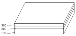
도 1 내지 도 6은 본 발명의 바람직한 제1 실시예에 따른 금속 나노입자들의 제조방법을 설명하기 위한 사시도들이다.
도 7 내지 도 11은 본 발명의 제1 실시예에 따른 제1 제조예를 설명하기 위한 이미지들이다.
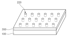
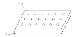
도 12 내지 도 16은 본 발명의 제2 실시예에 따른 금속 나노입자들의 제조방법을 설명하기 위한 사시도들이다.
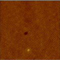
도 17 내지 도 19는 본 발명의 제2 실시예에 따른 제조예를 설명하기 위한 이미지들이다.FIGS. 1 to 6 are perspective views illustrating a method of manufacturing metal nanoparticles according to a first preferred embodiment of the present invention.
7 to 11 are images for explaining the first production example according to the first embodiment of the present invention.
12 to 16 are perspective views for explaining a method of manufacturing metal nanoparticles according to a second embodiment of the present invention.
17 to 19 are images for explaining a production example according to the second embodiment of the present invention.
본 발명은 다양한 변경을 가할 수 있고 여러 가지 형태를 가질 수 있는 바, 특정 실시예들을 도면에 예시하고 본문에 상세하게 설명하고자 한다. 그러나, 이는 본 발명을 특정한 개시 형태에 대해 한정하려는 것이 아니며, 본 발명의 사상 및 기술 범위에 포함되는 모든 변경, 균등물 내지 대체물을 포함하는 것으로 이해되어야 한다. 각 도면을 설명하면서 유사한 참조부호를 유사한 구성요소에 대해 사용하였다.The present invention is capable of various modifications and various forms, and specific embodiments are illustrated in the drawings and described in detail in the text. It should be understood, however, that the invention is not intended to be limited to the particular forms disclosed, but includes all modifications, equivalents, and alternatives falling within the spirit and scope of the invention. Like reference numerals are used for like elements in describing each drawing.
다르게 정의되지 않는 한, 기술적이거나 과학적인 용어를 포함해서 여기서 사용되는 모든 용어들은 본 발명이 속하는 기술 분야에서 통상의 지식을 가진 자에 의해 일반적으로 이해되는 것과 동일한 의미를 가지고 있다. 일반적으로 사용되는 사전에 정의되어 있는 것과 같은 용어들은 관련 기술의 문맥 상 가지는 의미와 일치하는 의미를 가지는 것으로 해석되어야 하며, 본 출원에서 명백하게 정의하지 않는 한, 이상적이거나 과도하게 형식적인 의미로 해석되지 않는다. Unless defined otherwise, all terms used herein, including technical or scientific terms, have the same meaning as commonly understood by one of ordinary skill in the art to which this invention belongs. Terms such as those defined in commonly used dictionaries are to be interpreted as having a meaning consistent with the contextual meaning of the related art and are to be interpreted as either ideal or overly formal in the sense of the present application Do not.
이하, 첨부한 도면들을 참조하여, 본 발명의 바람직한 실시예를 보다 상세하게 설명하고자 한다. Hereinafter, preferred embodiments of the present invention will be described in detail with reference to the accompanying drawings.
제1 실시예First Embodiment
도 1 내지 도 6은 본 발명의 바람직한 제1 실시예에 따른 금속 나노입자들의 제조방법을 설명하기 위한 사시도들이다.FIGS. 1 to 6 are perspective views illustrating a method of manufacturing metal nanoparticles according to a first preferred embodiment of the present invention.
도 1을 참조하면 기판(100) 상에 친수성 고분자층(200)과 고분자 자기조립층(300)을 형성한다.Referring to FIG. 1, a
기판(100)은 친수성 고분자층(200)과 고분자 자기조립층(300)의 형성에 적합한 강도와 재질을 가진 것이라면 어느 것이나 가능할 것이다. 다만, 상기 기판(100)은 표면 상에 형성되는 금속 나노입자를 수용할 수 있고, 화학적 처리 과정에서 기판(100)의 성질을 유지할 수 있는 재질이라면 어느 것이나 가능할 것이다.The
친수성 고분자층(200)을 형성하기 위해 친수성 고분자는 용매에 용해되고, 스핀 코팅 등의 방법을 통해 형성될 수 있다. 예컨대 상기 친수성 고분자층(200)은 PVA(Polyvinyl Alcohol)을 가질 수 있다. PVA를 친수성 고분자층(200)으로 사용하기 위해 PVA를 증류수에 1wt% 내지 3wt%의 농도로 용액을 제조하고, 이를 기판(100) 상에 스핀 코팅하여 친수성 고분자층(200)을 형성할 수 있다.In order to form the
친수성 고분자층(200) 상부에는 고분자 자기조립층(300)이 형성된다. 상기 고분자 자기조립층(200)은 PS-b-P2VP(Polystyrene-block-Poly-2-vinylpyridine copolymer)를 가질 수 있다. PS-b-P2VP는 블록 공중합체의 특성을 가지며, 톨루엔, THF 또는 클로로포름 등의 용매에서 0.1wt% 내지 5wt%의 농도로 혼합되고, 스핀 코팅 등을 통해 고분자 자기조립층(300)으로 형성된다.A polymer self-assembled layer (300) is formed on the hydrophilic polymer layer (200). The polymer self-assembled
도 2를 참조하면, 용매-증기 어닐링을 통해 고분자 자기조립층(300)을 매트릭스 영역(310)과 가용성 영역(320)으로 분리한다.Referring to FIG. 2, the polymer self-assembled
예컨대, 고분자 자기조립층(300)이 PS-b-P2VP로 구성된 경우, 용매-증기 어닐링을 통해 형성되는 매트릭스 영역(310)은 PS로 구성되고, 가용성 영역(320)은 P2VP로 구성된다. 용매-증기 어닐링을 위해 사용되는 용매는 클로로포름이 바람직하다. 클로로포름은 0.2ml 정도의 양으로 유리병에 투입되고, 10℃ 내지 100℃의 온도로 홀이 형성된 유리병을 통해 고분자 자기조립층에 증기의 형태로 공급된다. 만일 온도가 10℃ 미만이면 용매 증기의 발생량이 부족하여 가용성 영역과 매트릭스 영역의 분리가 충분히 일어나지 못한다. 또한, 온도가 100℃를 상회하면 고분자 자기조립층의 용해가 급격히 진행되어 매트릭스 영역과 가용성 영역을 형성이 곤란해진다.For example, when the polymer self-assembled
고분자 자기조립층(300)이 클로로포름 증기에 노출되면, 클로로포름 분자는 고분자 자기조립층(300)을 형성하는 PS-b-P2VP를 팽윤시키고 상분리를 유도한다. 따라서, 라인 형태의 가용성 영역(320)이 P2VP를 포함하면서 형성되고, 매트릭스 영역(310)은 PS로 형성된다.When the polymer self-assembled
도 3을 참조하면, 도 2에 개시된 구조물에 에탄올 등의 에천트를 도입하여 가용성 영역을 제거한다. 따라서, 라인 형태의 라인 홈(330)이 형성된 매트릭스 영역(310)을 얻을 수 있다. 만일, 가용성 영역이 P2VP로 구성된 경우, 에천트는 에탄올이 사용될 수 있다.Referring to FIG. 3, an etchant such as ethanol is introduced into the structure shown in FIG. 2 to remove the soluble region. Therefore, the
도 4를 참조하면, 식각 공정을 통해 친수성 고분자층(200)을 부분 식각하고, 하부에 배치된 기판(100)의 표면 일부를 노출시킨다. 식각 공정은 다양한 방법으로 이루어질 수 있으며, 산소 플라즈마 식각을 통해 수행됨이 바람직하다. 산소 플라즈마 식각을 이용하는 이유는 잔류할 수 있는 P2VP를 제거하기 위함이다. 즉, 상기 도 3에서 P2VP가 에탄올 등에 용해된다 하더라도 P2VP 분자의 말단은 PS 분자에 화학적으로 결합되어 완전히 제거되지 못한 상태에서 잔류하게 된다. 잔류하는 P2VP를 제거하고 식각 공정의 원활한 수행을 위해 산소 플라즈마 식각이 수행되면 P2VP는 완전히 제거되고, 잔류하는 PS 라인 패턴인 매트릭스 영역(310)을 식각 마스크로 이용하는 식각이 수행된다. 따라서, 상기 도 3에서 돌출된 형상의 PS 라인 패턴인 매트릭스 영역(310) 하부의 친수성 고분자층은 잔류하며, P2VP가 제거된 영역 하부의 친수성 고분자층은 제거되고, 기판(100)의 표면이 노출된다.Referring to FIG. 4, the
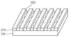
따라서, 기판(100) 상에 라인의 형태로 배치된 친수성 고분자 패턴(210)을 얻을 수 있으며, 각각의 친수성 고분자 패턴들(210) 사이의 이격공간에서는 기판(100)이 노출된다.Accordingly, a
도 5를 참조하면, 라인 형태의 친수성 고분자 패턴(210) 사이에 금속 전구체를 포함하는 마이셀(400)을 형성한다. 마이셀(400)은 PS-b-P4VP(Polystyrene-b-poly(4-vinylpyridine) copolymer)에 금속 전구체가 화학적으로 결합된 형태일 수 있다. 먼저, PS-b-P4VP를 톨루엔에 0.05wt% 내지 2wt%로 용해하고, 금속 이온을 투입한다. 제조된 용액을 상기 도 4에 개시된 구조물 상에 도포한다. 도포는 스핀 코팅법에 따른다. 이를 통해 친수성 고분자 패턴(210) 사이에 일정한 간격으로 형성된 금속 전구체를 포함하는 마이셀(400)을 얻을 수 있다. 상기 도 5에서 친수성 고분자 패턴(210)은 금속 전구체를 포함하는 마이셀(400)의 위치와 이격 거리를 결정하는데 사용된다. 또한, 마이셀(400)은 외부는 PS로 구성되고, 내부는 P4VP로 구성된다. 또한, P4VP는 금속 전구체와 결합된 형태로 제공된다. 이러한 마이셀(400)의 구조는 PS-b-P4VP에 금속 이온 M-가 결합된 구조이다. 즉, P4VP에 금속 이온 M-가 결합된 양상으로 나타나며, 이는 화학식 1에 개시된다.Referring to FIG. 5, a
[화학식 1][Chemical Formula 1]

상기 화학식 1에서 나타난 바와 같이 마이셀(400)의 외곽을 형성하는 PS(Polystyrene)은 소수성의 특징을 가진다. 또한, 이러한 마이셀(400)은 친수성 고분자 패턴(210)을 피해 기판(100) 상에 형성되며, 친수성 고분자 패턴(210)의 이격 공간 사이에 배치되는 마이셀(400)은 도포 용액의 농도가 높을수록 배치되는 마이셀(400)의 개수는 증가한다. 즉 도포 용액에서 마이셀(400)의 농도가 높을수록 친수성 고분자 패턴들(210)의 이격 공간에 배치되는 마이셀(400)의 간격은 작아지는 경향을 가진다.As shown in Formula 1, PS (Polystyrene) forming the outer surface of the
도 6을 참조하면, 상기 도 5에 개시된 구조물에서 친수성 고분자 패턴을 제거한다. 친수성 고분자 패턴의 제거는 친수성 성질을 가진 물 또는 알콜류 등의 도입을 통해 구현된다. 친수성 고분자 패턴의 제거를 통해 기판(100) 상에 일정한 간격의 규칙적 배열을 가지는 마이셀들을 얻을 수 있다.Referring to FIG. 6, the hydrophilic polymer pattern is removed from the structure shown in FIG. Removal of the hydrophilic polymer pattern is achieved through the introduction of water or alcohols having hydrophilic properties. By removing the hydrophilic polymer pattern, it is possible to obtain micelles having a regular arrangement of regular intervals on the
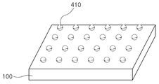
계속해서 기판(100) 상에 형성된 마이셀에서 PS-b-P4VP를 제거하고 환원반응을 통해 금속 전구체를 금속 나노입자(410)로 전환한다. 마이셀에서의 고분자의 제거 및 금속 전구체의 환원은 산소 플라즈마를 통한 식각에 의해 수행된다. 이를 통해 기판(100) 상에 규칙적인 배열을 가진 금속 나노입자(410)를 얻을 수 있다. 형성되는 금속 나노입자는 금, 백금, 팔라듐 등 다양한 양상을 가지며, 마이셀을 구성하는 고분자에 결합할 수 있는 금속이라면 어느 것이나 가능할 것이다.Subsequently, PS-b-P4VP is removed from the micelle formed on the
제1 제조예First Production Example
도 7 내지 도 11은 본 발명의 제1 실시예에 따른 제1 제조예를 설명하기 위한 이미지들이다.7 to 11 are images for explaining the first production example according to the first embodiment of the present invention.
먼저, 실리콘 기판 상에 PVA를 이용하여 친수성 고분자층을 형성한다. 친수성 고분자층 상에 PS-b-P2VP를 이용하여 고분자 자기조립층을 형성한다. 또한, 클로르포름 용매를 사용한 어닐링이 수행된다. 어닐링 온도는 35℃이며, 2시간 수행된다.First, a hydrophilic polymer layer is formed on a silicon substrate using PVA. A polymer self-assembled layer is formed on the hydrophilic polymer layer using PS-b-P2VP. Annealing with a chloroform solvent is also performed. The annealing temperature is 35 DEG C and is performed for 2 hours.
도 7은 어닐링을 통해 상분리가 일어난 상태를 도시한 이미지이다. 상기 이미지에서 P2VP는 PS로부터 상분리가 되고, 대략 지문 형태의 라인 패턴으로 형성된 것을 알 수 있다.7 is an image showing a state where phase separation has occurred through annealing. It can be seen from the image that P2VP is phase separated from PS and formed in a line pattern of approximately fingerprint type.
도 8을 참조하면, 라인형태의 P2VP 패턴이 형성된 기판을 알코올이 포함된 용액에 투입하고, 기판 상에 잔류하는 알코올을 블로잉(blowing) 과정을 통해 제거한다. 이를 통해 P2VP 패턴은 제거되고, 제거된 상태는 짙은 색의 오목부로 나타난다.Referring to FIG. 8, a substrate having a line-shaped P2VP pattern formed thereon is introduced into a solution containing alcohol, and the alcohol remaining on the substrate is removed through a blowing process. Through this, the P2VP pattern is removed, and the removed state appears as a dark colored concavity.
도 9는 잔류하는 PS 패턴을 식각 마스크로 이용하여 산소 플라즈마 식각을 수행한 이미지이며, 도 10 및 도 11은 식각을 통해 형성된 PVA 라인 패턴들 사이의 이격공간에 PS-b-P4VP를 포함하는 마이셀들을 배치한다. 도 10은 PS-b-P4VP를 0.1wt%의 농도로 스핀 코팅한 경우의 이미지이고, 도 11은 PS-b-P4VP의 농도를 0.15wt%의 농도로 스핀 코팅한 경우의 이미지이다. 마이셀의 농도가 높을수록 마이셀 입자들의 간격은 조밀해짐을 알 수 있다.FIG. 9 is an image obtained by performing oxygen plasma etching using the residual PS pattern as an etch mask. FIG. 10 and FIG. 11 are graphs showing the relationship between the thicknesses of PVA line patterns formed through etching, . 10 is an image obtained by spin-coating PS-b-P4VP at a concentration of 0.1 wt%, and FIG. 11 is an image obtained by spin coating a PS-b-P4VP concentration at a concentration of 0.15 wt%. The higher the micelle concentration, the more dense the micelle particles are.
제2 실시예Second Embodiment
도 12 내지 도 16은 본 발명의 제2 실시예에 따른 금속 나노입자들의 제조방법을 설명하기 위한 사시도들이다.12 to 16 are perspective views for explaining a method of manufacturing metal nanoparticles according to a second embodiment of the present invention.
먼저, 제1 실시예의 도 1에 언급된 바대로 기판(100) 상에 친수성 고분자층(200)과 고분자 자기조립층(300)을 순차적으로 형성한다. 친수성 고분자층(200)은 PVA를 가지며, 고분자 자기조립층(300)은 PS-b-P2VP를 가질 수 있다.First, a
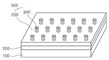
도 12를 참조하면, 도 1에 개시된 고분자 자기조립층(300)에 대해 용매-증기 어닐링을 수행하여 매트릭스 영역(330) 내에 도트 형상의 가용성 영역(340)을 형성한다. 고분자 자기조립층(300)이 PS-b-P2VP로 구성된 경우, 용매-증기 어닐링을 위한 용매로는 THF(Tetrahydrofuran)가 사용될 수 있다. 유리병 등의 적절한 용기에 THF를 투입하고, 10℃ 내지 100℃의 온도로 홀이 형성된 유리병을 통해 고분자 자기조립층에 증기의 형태로 공급된다. 만일 온도가 10℃ 미만이면 용매 증기의 발생량이 부족하여 가용성 영역과 매트릭스 영역의 분리가 충분히 일어나지 못한다. 또한, 온도가 100℃를 상회하면 고분자 자기조립층의 용해가 급격히 진행되어 매트릭스 영역과 가용성 영역을 형성이 곤란해진다. Referring to FIG. 12, solvent-vapor annealing is performed on the polymer self-assembled
THF는 P2VP보다 PS를 화학적으로 더 용해시키는 특징이 있다. 따라서, PS는 THF에 의해 먼저 용해되고, 분자결합이 끊어진 P2VP는 응집되어 도트 형상의 가용성 영역(340)을 형성한다.THF is more chemically dissolving PS than P2VP. Thus, PS is first dissolved by THF and P2VP, which breaks the molecular bond, aggregates to form dot-shaped
즉, 제1 실시예 및 제2 실시예에서의 용매-증기 어닐링을 통해 특정의 고분자들은 라인 형태 또는 도트 형태로 응집되고, 이는 가용성 영역(340)을 형성한다. 형성된 가용성 영역(340)은 매트릭스 영역(330)에 비해 특정의 에천트에 대한 선택성을 가지다. 즉, 특정의 에천트가 고분자 자기조립층(300)에 도입되는 경우, 가용성 영역(340)은 매트릭스 영역(330)에 비해 높은 용해도를 가지고, 에천트의 도입에 따라 제거되는 특징이 있다.That is, through the solvent-vapor annealing in the first embodiment and the second embodiment, the specific polymers are aggregated in the form of a line or a dot, which forms the
도 13을 참조하면, 에탄올 등의 에천트에 도 12의 구조물을 침지시키거나 에천트를 가용성 영역에 도입하여 가용성 영역을 제거한다. 따라서, 대략 도트 형태의 다수개의 도트 홀들(350)이 형성되고, PS로 구성된 매트릭스 영역(330)이 잔류한다. 따라서, 친수성 고분자층 상에는 매트릭스 영역이 잔류하며, 매트릭스 영역 내에는 친수성 고분자층의 표면 일부를 노출하는 도트 홀들(350)이 형성된다.Referring to FIG. 13, the structure of FIG. 12 is immersed in an etchant such as ethanol, or an etchant is introduced into a soluble region to remove a soluble region. Therefore, a plurality of dot holes 350 of approximately dot shape are formed, and the
도 14를 참조하면, 상기 도 13에서 잔류하는 매트릭스 영역을 식각 마스크로 이용하여 친수성 고분자층(200)을 식각한다. 상기 식각은 산소 플라즈마 식각을 이용한다. 따라서, 진공상태에서 발생되는 산소 플라즈마를 공급하여 친수성 고분자층(200)을 식각한다. 산소 플라즈마 식각의 이용을 통해 도 12의 홀 내부에 잔류하는 P2VP는 제거될 수 있다. 상기 도 13의 도트 홀들은 친수성 고분자층(200)에 전사되어 패턴 홀(220)이 형성되고, 식각을 통해 기판 표면의 일부는 노출된다.Referring to FIG. 14, the
도 15를 참조하면, 친수성 고분자층(200)의 도트 형태의 패턴 홀(220) 내부에 금속 전구체를 포함하는 마이셀(400)을 형성한다. 각각의 패턴 홀(220) 내부에는 적어도 하나의 마이셀(400)이 배치된다. 마이셀(400)은 PS-b-P4VP에 금속 전구체가 화학적으로 결합된 형태일 수 있다. 먼저, PS-b-P4VP를 톨루엔에 0.05wt% 내지 2wt%로 용해하고, 제조된 용액을 상기 도 14에 개시된 구조물 상에 도포한다. 도포는 스핀 코팅법에 따른다. 이를 통해 친수성 고분자층(200)의 패턴 홀(220) 내부에 형성된 금속 전구체 마이셀(400)을 얻을 수 있다. 마이셀(400)은 외부는 PS로 구성되고, 내부는 P4VP로 구성된다. 또한, P4VP는 금속 전구체와 결합된 형태로 제공된다. 이러한 마이셀(400)의 구조는 상기의 화학식 1과 같다.Referring to FIG. 15, a
도 16을 참조하면, 도 15에 개시된 구조물에서 친수성 고분자층을 제거한다. 친수성 고분자층의 제거는 친수성 성질을 가진 물 또는 알콜류 등의 도입을 통해 구현된다. 친수성 고분자층의 제거를 통해 기판(100) 상에 일정한 배열을 가지는 마이셀들을 얻을 수 있다.Referring to FIG. 16, the hydrophilic polymer layer is removed from the structure shown in FIG. Removal of the hydrophilic polymer layer is achieved through the introduction of water or alcohols having hydrophilic properties. By removing the hydrophilic polymer layer, micelles having a uniform arrangement on the
계속해서 기판(100) 상에 형성된 마이셀에서 PS-b-P4VP를 제거하고 환원반응을 통해 금속 전구체를 금속 나노입자(410)로 전환한다. 마이셀에서 고분자의 제거 및 금속 전구체의 환원은 산소 플라즈마를 통한 식각에 의해 수행된다. 이를 통해 기판(100) 상에 도트 형태의 배열을 가진 금속 나노입자(410)를 얻을 수 있다.Subsequently, PS-b-P4VP is removed from the micelle formed on the
제2 제조예Example 2
도 17 내지 도 19는 본 발명의 제2 실시예에 따른 제조예를 설명하기 위한 이미지들이다.17 to 19 are images for explaining a production example according to the second embodiment of the present invention.
실리콘 기판 상에 PVA를 사용하여 친수성 고분자층을 형성하고, 그 상부에 PS-b-P2VP를 이용하여 고분자 자기조립층을 형성한다. 또한, THF를 용매로 이용한 어닐링이 수행된다.A hydrophilic polymer layer is formed on the silicon substrate using PVA, and a polymer self-assembled layer is formed on the hydrophilic polymer layer using PS-b-P2VP. Further, annealing is performed using THF as a solvent.
도 17은 용매-증기 어닐링을 통해 상분리가 일어난 상태를 도시한 이미지이다. 어닐링 온도는 35℃이며, 2시간 30분 동안 용매-증기 어닐링이 수행된다. 상기 이미지 상으로 도트 형태의 밝은 부분은 P2VP가 응집된 형상을 나타낸다.17 is an image showing a phase-separated state through solvent-vapor annealing. The annealing temperature is 35 占 폚 and solvent-vapor annealing is performed for 2 hours 30 minutes. The bright portion of the dot shape on the image shows the P2VP aggregated shape.
또한, 17에 도시된 시료를 알코올에 침지시킨 후, 블로잉을 통해 표면 상의 알코올을 제거한다. 알코올의 이용에 따라 도트 형태의 P2VP의 상당 부분은 제거되고 홀이 형성된다. 이는 도 18에 도시되고 있으며, 어두운 색으로 홀의 형성을 알 수 있다.In addition, the sample shown in Fig. 17 is immersed in alcohol, and then the alcohol on the surface is removed by blowing. Depending on the use of alcohol, much of the dotted P2VP is removed and holes are formed. This is shown in FIG. 18, which shows the formation of holes with a dark color.
도 19는 마이셀을 PS-b-P4VP 34k를 이용하여 PVA로 구성된 친수성 고분자층의 홀 내부의 이미지를 도시한 것이다. 홀 내부에는 마이셀의 직경은 36nm이며, 3개의 마이셀들이 배치되고 있다. 또한, 친수성 고분자층의 홀의 직경과 홀 내부에 삽입하려는 마이셀의 직경 사이의 크기비에 따라 삽입되는 마이셀의 개수가 조절 가능하다.19 shows an image of a hole inside the hydrophilic polymer layer composed of PVA using PS-b-P4VP 34k as a micelle. Inside the hole, the diameter of the micelle is 36 nm, and three micelles are arranged. In addition, the number of inserted micelles can be adjusted according to the size ratio between the diameter of the hole of the hydrophilic polymer layer and the diameter of the micelle to be inserted into the hole.
상술한 본 발명에서는 고분자 자기조립층에 대한 용매-증기 어닐링을 통해 다양한 형상의 가용성 영역을 형성할 수 있다. 가용성 영역은 매트릭스 영역에 대한 식각 선택성 또는 용매 선택성을 가진다. 이를 근거로 소정의 패턴을 기판 상에 형성할 수 있으며, 마이셀의 도입을 통해 일정한 간격을 가지는 금속 나노입자들을 얻을 수 있다. 형성되는 금속 나노입자들은 기판 상에 형성되며, 금, 백금, 팔라듐 또는 은 등 다양한 양상을 가질 수 있다. 또한, 형성되는 금속 나노입자들은 촉매 등으로 사용될 수 있으며, 형성된 촉매는 화학반응에서 접촉면적의 향상을 유발할 수 있다.In the present invention described above, soluble regions of various shapes can be formed through solvent-vapor annealing of the polymer self-assembled layer. The soluble region has etch selectivity or solvent selectivity to the matrix region. Based on this, a predetermined pattern can be formed on the substrate, and metal nanoparticles having a certain interval can be obtained through introduction of micelles. The metal nanoparticles to be formed are formed on the substrate and may have various forms such as gold, platinum, palladium or silver. Also, the metal nanoparticles to be formed can be used as a catalyst, and the formed catalyst can cause an increase in the contact area in a chemical reaction.
100 : 기판
200 : 친수성 고분자층
300 : 고분자 자기조립층
310, 330 : 매트릭스 영역
320, 340 : 가용성 영역
400 : 마이셀100: substrate 200: hydrophilic polymer layer
300: polymer self-assembled
320, 340: Availability area 400: Michel
Claims (8)
상기 고분자 자기조립층에 대한 용매-증기 어닐링을 수행하여, 상기 고분자 자기조립층을 매트릭스 영역과 상기 매트릭스 영역에 대해 식각 선택성을 가지는 가용성 영역으로 분리하는 단계;
상기 가용성 영역을 제거하고, 상기 매트릭스 영역을 잔류시키는 단계;
상기 잔류하는 매트릭스 영역을 식각 마스크로 이용하여 상기 고분자 자기조립층의 일부를 식각하여 라인 형태의 친수성 고분자 패턴을 형성하고 상기 기판의 일부를 노출시키는 단계;
상기 친수성 고분자 패턴들 사이의 이격 공간에 금속 전구체를 포함하는 마이셀을 형성하는 단계; 및
상기 마이셀에 대한 산소 플라즈마 식각을 통해 금속 나노입자를 형성하는 단계를 포함하는 금속 나노입자의 형성방법.Sequentially forming a hydrophilic polymer layer and a polymer self-assembled layer on a substrate;
Performing solvent-vapor annealing on the polymer self-assembled layer to separate the polymer self-assembled layer into a matrix region and a soluble region having etch selectivity with respect to the matrix region;
Removing the soluble region and leaving the matrix region;
Etching a part of the polymer self-assembled layer using the remaining matrix region as an etch mask to form a line-shaped hydrophilic polymer pattern and exposing a part of the substrate;
Forming a micelle containing a metal precursor in a spacing space between the hydrophilic polymer patterns; And
And forming metal nanoparticles through the oxygen plasma etching on the micelles.
상기 고분자 자기조립층에 대한 용매-증기 어닐링을 수행하여, 상기 고분자 자기조립층을 매트릭스 영역과 상기 매트릭스 영역에 대해 식각 선택성을 가지고, 도트 형상의 가용성 영역으로 분리하는 단계;
상기 가용성 영역을 제거하고, 상기 매트릭스 영역을 잔류시키며, 상기 매트릭스 영역 내에 도트 홀들을 형성하는 단계;
상기 잔류하는 매트릭스 영역을 식각 마스크로 이용하여 상기 고분자 자기조립층의 일부를 식각하여 도트 형태의 친수성 고분자 패턴을 형성하고 상기 기판의 일부를 노출시키는 패턴 홀들을 형성하는 단계;
상기 패턴 홀 내에 금속 전구체를 포함하는 마이셀을 형성하는 단계; 및
상기 마이셀에 대한 산소 플라즈마 식각을 통해 금속 나노입자를 형성하는 단계를 포함하는 금속 나노입자의 형성방법.Sequentially forming a hydrophilic polymer layer and a polymer self-assembled layer on a substrate;
Performing solvent-vapor annealing of the polymer self-assembled layer to separate the polymer self-assembled layer into a dot-shaped soluble region having an etch selectivity with respect to the matrix region and the matrix region;
Removing the soluble region, leaving the matrix region, and forming dot holes in the matrix region;
Forming a patterned hydrophilic polymer pattern by etching a part of the polymer self-assembled layer using the remaining matrix region as an etch mask and forming pattern holes exposing a part of the substrate;
Forming a micelle including a metal precursor in the pattern hole; And
And forming metal nanoparticles through the oxygen plasma etching on the micelles.
Priority Applications (1)
| Application Number | Priority Date | Filing Date | Title |
|---|---|---|---|
| KR1020150088200A KR101830476B1 (en) | 2015-06-22 | 2015-06-22 | Method of Forming Regular Array of Metal Nanoparticles |
Applications Claiming Priority (1)
| Application Number | Priority Date | Filing Date | Title |
|---|---|---|---|
| KR1020150088200A KR101830476B1 (en) | 2015-06-22 | 2015-06-22 | Method of Forming Regular Array of Metal Nanoparticles |
Publications (2)
| Publication Number | Publication Date |
|---|---|
| KR20170000009A true KR20170000009A (en) | 2017-01-02 |
| KR101830476B1 KR101830476B1 (en) | 2018-02-21 |
Family
ID=57810368
Family Applications (1)
| Application Number | Title | Priority Date | Filing Date |
|---|---|---|---|
| KR1020150088200A Expired - Fee Related KR101830476B1 (en) | 2015-06-22 | 2015-06-22 | Method of Forming Regular Array of Metal Nanoparticles |
Country Status (1)
| Country | Link |
|---|---|
| KR (1) | KR101830476B1 (en) |
Cited By (2)
| Publication number | Priority date | Publication date | Assignee | Title |
|---|---|---|---|---|
| CN110943040A (en) * | 2018-09-21 | 2020-03-31 | 三星电子株式会社 | Method of dicing substrate and separation method for forming semiconductor chip |
| KR20230143809A (en) * | 2022-04-06 | 2023-10-13 | 한국화학연구원 | A Current Collector for a Lithium Metal Battery Having an Intaglio Pattern, a Manufacturing Method Thereof, and a Lithium Metal Battery Including The Same |
Families Citing this family (1)
| Publication number | Priority date | Publication date | Assignee | Title |
|---|---|---|---|---|
| KR102963863B1 (en) * | 2019-11-26 | 2026-05-11 | 재단법인 포항산업과학연구원 | Apparatus for Collecting Condensate and Manufacturing Method thereof |
Family Cites Families (2)
| Publication number | Priority date | Publication date | Assignee | Title |
|---|---|---|---|---|
| KR101238551B1 (en) | 2010-09-29 | 2013-03-04 | 한국과학기술원 | Method for manufacturing nanoparticle array, nanoparticle array manufactured by the same, method for manufacturing bio-sensor having plasmonic nanoparticles, method for sensing bio-material using the bio-sensor |
| KR101412228B1 (en) | 2012-06-11 | 2014-07-02 | 한국과학기술원 | Method for manufacturing thin film comprising mixed block copolymer, method for manufacturing template comprising mixed block copolymer, and thin film and template mixed block copolymer |
-
2015
- 2015-06-22 KR KR1020150088200A patent/KR101830476B1/en not_active Expired - Fee Related
Cited By (2)
| Publication number | Priority date | Publication date | Assignee | Title |
|---|---|---|---|---|
| CN110943040A (en) * | 2018-09-21 | 2020-03-31 | 三星电子株式会社 | Method of dicing substrate and separation method for forming semiconductor chip |
| KR20230143809A (en) * | 2022-04-06 | 2023-10-13 | 한국화학연구원 | A Current Collector for a Lithium Metal Battery Having an Intaglio Pattern, a Manufacturing Method Thereof, and a Lithium Metal Battery Including The Same |
Also Published As
| Publication number | Publication date |
|---|---|
| KR101830476B1 (en) | 2018-02-21 |
Similar Documents
| Publication | Publication Date | Title |
|---|---|---|
| TWI392643B (en) | Method for selectively penetrating a self-assembled block copolymer by using a metal oxide, a method for forming a metal oxide structure, and a semiconductor structure including the same | |
| US8399174B2 (en) | Method of forming fine patterns using a block copolymer | |
| TWI359458B (en) | Alternating self-assembling morphologies of dibloc | |
| CN102983065B (en) | Pattern, mask pattern forming method and method, semi-conductor device manufacturing method | |
| EP2948817B1 (en) | Surface nanofabrication methods using self-assembled polymer nanomasks | |
| JP4923904B2 (en) | Method for producing a substrate with different hydrophilic and / or lipophilic regions on the same surface | |
| WO2016065308A1 (en) | Nanoshape patterning techniques that allow high-speed and low-cost fabrication of nanoshape structures | |
| KR20090083091A (en) | Micro pattern formation method using block copolymer | |
| TW201008867A (en) | Graphoepitaxial self-assembly of arrays of downward facing half-cylinders | |
| US11923197B2 (en) | Methods of forming nanostructures utilizing self-assembled nucleic acids | |
| CN101432224A (en) | Substrate with microfine metallic lumps arranged on surface | |
| KR101830476B1 (en) | Method of Forming Regular Array of Metal Nanoparticles | |
| US12002861B2 (en) | Method of forming conductive contacts on graphene | |
| CN105278240A (en) | Methods for manufacturing block copolymers and articles manufactured therefrom | |
| US20080280099A1 (en) | Silicon Substrates with Thermal Oxide Windows for Transmission Electron Microscopy | |
| CN107258009A (en) | Method for wet etching block copolymer self-assembled patterns | |
| KR20150092397A (en) | Block copolymer and method of forming the same | |
| CN117701373A (en) | Sequencing chip and preparation method thereof | |
| KR20100111525A (en) | Method for fabricating nanopattern embedding nanoparticles, and electronic device | |
| KR101989414B1 (en) | Metal nanowires in micropatterns using block copolymers and preparing method thereof | |
| KR20150143222A (en) | Method Pattenring silica particle and Pattenring silica particle by using thereof | |
| TW201920323A (en) | Process for controlling the orientation of the nanodomains of a block copolymer | |
| JP2009081369A (en) | Stencil mask manufacturing method | |
| KR20220096324A (en) | Method for alignment of block copolymer using superfine pattern | |
| US11803120B2 (en) | Graphene-enabled block copolymer lithography transfer to arbitrary surfaces |
Legal Events
| Date | Code | Title | Description |
|---|---|---|---|
| PA0109 | Patent application |
St.27 status event code: A-0-1-A10-A12-nap-PA0109 |
|
| A201 | Request for examination | ||
| PA0201 | Request for examination |
St.27 status event code: A-1-2-D10-D11-exm-PA0201 |
|
| PG1501 | Laying open of application |
St.27 status event code: A-1-1-Q10-Q12-nap-PG1501 |
|
| D13-X000 | Search requested |
St.27 status event code: A-1-2-D10-D13-srh-X000 |
|
| D14-X000 | Search report completed |
St.27 status event code: A-1-2-D10-D14-srh-X000 |
|
| E902 | Notification of reason for refusal | ||
| PE0902 | Notice of grounds for rejection |
St.27 status event code: A-1-2-D10-D21-exm-PE0902 |
|
| E13-X000 | Pre-grant limitation requested |
St.27 status event code: A-2-3-E10-E13-lim-X000 |
|
| P11-X000 | Amendment of application requested |
St.27 status event code: A-2-2-P10-P11-nap-X000 |
|
| P13-X000 | Application amended |
St.27 status event code: A-2-2-P10-P13-nap-X000 |
|
| E701 | Decision to grant or registration of patent right | ||
| PE0701 | Decision of registration |
St.27 status event code: A-1-2-D10-D22-exm-PE0701 |
|
| GRNT | Written decision to grant | ||
| PR0701 | Registration of establishment |
St.27 status event code: A-2-4-F10-F11-exm-PR0701 |
|
| PR1002 | Payment of registration fee |
St.27 status event code: A-2-2-U10-U11-oth-PR1002 Fee payment year number: 1 |
|
| PG1601 | Publication of registration |
St.27 status event code: A-4-4-Q10-Q13-nap-PG1601 |
|
| P22-X000 | Classification modified |
St.27 status event code: A-4-4-P10-P22-nap-X000 |
|
| R18-X000 | Changes to party contact information recorded |
St.27 status event code: A-5-5-R10-R18-oth-X000 |
|
| PR1001 | Payment of annual fee |
St.27 status event code: A-4-4-U10-U11-oth-PR1001 Fee payment year number: 4 |
|
| PR1001 | Payment of annual fee |
St.27 status event code: A-4-4-U10-U11-oth-PR1001 Fee payment year number: 5 |
|
| PR1001 | Payment of annual fee |
St.27 status event code: A-4-4-U10-U11-oth-PR1001 Fee payment year number: 6 |
|
| P14-X000 | Amendment of ip right document requested |
St.27 status event code: A-5-5-P10-P14-nap-X000 |
|
| PN2301 | Change of applicant |
St.27 status event code: A-5-5-R10-R11-asn-PN2301 |
|
| P16-X000 | Ip right document amended |
St.27 status event code: A-5-5-P10-P16-nap-X000 |
|
| PN2301 | Change of applicant |
St.27 status event code: A-5-5-R10-R14-asn-PN2301 |
|
| PR1001 | Payment of annual fee |
St.27 status event code: A-4-4-U10-U11-oth-PR1001 Fee payment year number: 7 |
|
| R18-X000 | Changes to party contact information recorded |
St.27 status event code: A-5-5-R10-R18-oth-X000 |
|
| R18-X000 | Changes to party contact information recorded |
St.27 status event code: A-5-5-R10-R18-oth-X000 |
|
| PC1903 | Unpaid annual fee |
St.27 status event code: A-4-4-U10-U13-oth-PC1903 Not in force date: 20250213 Payment event data comment text: Termination Category : DEFAULT_OF_REGISTRATION_FEE |
|
| H13 | Ip right lapsed |
Free format text: ST27 STATUS EVENT CODE: N-4-6-H10-H13-OTH-PC1903 (AS PROVIDED BY THE NATIONAL OFFICE); TERMINATION CATEGORY : DEFAULT_OF_REGISTRATION_FEE Effective date: 20250213 |
|
| PC1903 | Unpaid annual fee |
St.27 status event code: N-4-6-H10-H13-oth-PC1903 Ip right cessation event data comment text: Termination Category : DEFAULT_OF_REGISTRATION_FEE Not in force date: 20250213 |
|
| R18 | Changes to party contact information recorded |
Free format text: ST27 STATUS EVENT CODE: A-5-5-R10-R18-OTH-X000 (AS PROVIDED BY THE NATIONAL OFFICE) |
|
| R18-X000 | Changes to party contact information recorded |
St.27 status event code: A-5-5-R10-R18-oth-X000 |