KR20170000009A - 금속 나노입자의 규칙배열 형성방법 - Google Patents
금속 나노입자의 규칙배열 형성방법 Download PDFInfo
- Publication number
- KR20170000009A KR20170000009A KR1020150088200A KR20150088200A KR20170000009A KR 20170000009 A KR20170000009 A KR 20170000009A KR 1020150088200 A KR1020150088200 A KR 1020150088200A KR 20150088200 A KR20150088200 A KR 20150088200A KR 20170000009 A KR20170000009 A KR 20170000009A
- Authority
- KR
- South Korea
- Prior art keywords
- polymer
- layer
- assembled layer
- forming
- region
- Prior art date
- Legal status (The legal status is an assumption and is not a legal conclusion. Google has not performed a legal analysis and makes no representation as to the accuracy of the status listed.)
- Granted
Links
Images








Classifications
-
- B—PERFORMING OPERATIONS; TRANSPORTING
- B22—CASTING; POWDER METALLURGY
- B22F—WORKING METALLIC POWDER; MANUFACTURE OF ARTICLES FROM METALLIC POWDER; MAKING METALLIC POWDER; APPARATUS OR DEVICES SPECIALLY ADAPTED FOR METALLIC POWDER
- B22F9/00—Making metallic powder or suspensions thereof
- B22F9/16—Making metallic powder or suspensions thereof using chemical processes
- B22F9/18—Making metallic powder or suspensions thereof using chemical processes with reduction of metal compounds
- B22F9/24—Making metallic powder or suspensions thereof using chemical processes with reduction of metal compounds starting from liquid metal compounds, e.g. solutions
-
- B—PERFORMING OPERATIONS; TRANSPORTING
- B82—NANOTECHNOLOGY
- B82B—NANOSTRUCTURES FORMED BY MANIPULATION OF INDIVIDUAL ATOMS, MOLECULES, OR LIMITED COLLECTIONS OF ATOMS OR MOLECULES AS DISCRETE UNITS; MANUFACTURE OR TREATMENT THEREOF
- B82B3/00—Manufacture or treatment of nanostructures by manipulation of individual atoms or molecules, or limited collections of atoms or molecules as discrete units
- B82B3/0009—Forming specific nanostructures
- B82B3/0014—Array or network of similar nanostructural elements
-
- B—PERFORMING OPERATIONS; TRANSPORTING
- B82—NANOTECHNOLOGY
- B82B—NANOSTRUCTURES FORMED BY MANIPULATION OF INDIVIDUAL ATOMS, MOLECULES, OR LIMITED COLLECTIONS OF ATOMS OR MOLECULES AS DISCRETE UNITS; MANUFACTURE OR TREATMENT THEREOF
- B82B3/00—Manufacture or treatment of nanostructures by manipulation of individual atoms or molecules, or limited collections of atoms or molecules as discrete units
- B82B3/0009—Forming specific nanostructures
- B82B3/0038—Manufacturing processes for forming specific nanostructures not provided for in groups B82B3/0014 - B82B3/0033
-
- C—CHEMISTRY; METALLURGY
- C08—ORGANIC MACROMOLECULAR COMPOUNDS; THEIR PREPARATION OR CHEMICAL WORKING-UP; COMPOSITIONS BASED THEREON
- C08F—MACROMOLECULAR COMPOUNDS OBTAINED BY REACTIONS ONLY INVOLVING CARBON-TO-CARBON UNSATURATED BONDS
- C08F299/00—Macromolecular compounds obtained by interreacting polymers involving only carbon-to-carbon unsaturated bond reactions, in the absence of non-macromolecular monomers
-
- B—PERFORMING OPERATIONS; TRANSPORTING
- B22—CASTING; POWDER METALLURGY
- B22F—WORKING METALLIC POWDER; MANUFACTURE OF ARTICLES FROM METALLIC POWDER; MAKING METALLIC POWDER; APPARATUS OR DEVICES SPECIALLY ADAPTED FOR METALLIC POWDER
- B22F2202/00—Treatment under specific physical conditions
- B22F2202/13—Use of plasma
-
- B—PERFORMING OPERATIONS; TRANSPORTING
- B82—NANOTECHNOLOGY
- B82Y—SPECIFIC USES OR APPLICATIONS OF NANOSTRUCTURES; MEASUREMENT OR ANALYSIS OF NANOSTRUCTURES; MANUFACTURE OR TREATMENT OF NANOSTRUCTURES
- B82Y40/00—Manufacture or treatment of nanostructures
Landscapes
- Chemical & Material Sciences (AREA)
- Engineering & Computer Science (AREA)
- Nanotechnology (AREA)
- Crystallography & Structural Chemistry (AREA)
- Chemical Kinetics & Catalysis (AREA)
- Manufacturing & Machinery (AREA)
- Health & Medical Sciences (AREA)
- Medicinal Chemistry (AREA)
- Polymers & Plastics (AREA)
- Organic Chemistry (AREA)
- General Chemical & Material Sciences (AREA)
- Chemically Coating (AREA)
- Catalysts (AREA)
Abstract
Description
도 7 내지 도 11은 본 발명의 제1 실시예에 따른 제1 제조예를 설명하기 위한 이미지들이다.
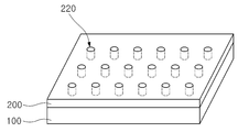
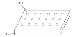
도 12 내지 도 16은 본 발명의 제2 실시예에 따른 금속 나노입자들의 제조방법을 설명하기 위한 사시도들이다.
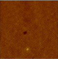
도 17 내지 도 19는 본 발명의 제2 실시예에 따른 제조예를 설명하기 위한 이미지들이다.

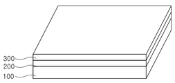
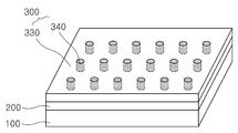
300 : 고분자 자기조립층 310, 330 : 매트릭스 영역
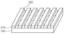
320, 340 : 가용성 영역 400 : 마이셀
Claims (8)
- 기판 상에 친수성 고분자층 및 고분자 자기조립층을 순차적으로 형성하는 단계;
상기 고분자 자기조립층에 대한 용매-증기 어닐링을 수행하여, 상기 고분자 자기조립층을 매트릭스 영역과 상기 매트릭스 영역에 대해 식각 선택성을 가지는 가용성 영역으로 분리하는 단계;
상기 가용성 영역을 제거하고, 상기 매트릭스 영역을 잔류시키는 단계;
상기 잔류하는 매트릭스 영역을 식각 마스크로 이용하여 상기 고분자 자기조립층의 일부를 식각하여 라인 형태의 친수성 고분자 패턴을 형성하고 상기 기판의 일부를 노출시키는 단계;
상기 친수성 고분자 패턴들 사이의 이격 공간에 금속 전구체를 포함하는 마이셀을 형성하는 단계; 및
상기 마이셀에 대한 산소 플라즈마 식각을 통해 금속 나노입자를 형성하는 단계를 포함하는 금속 나노입자의 형성방법. - 제1항에 있어서, 상기 고분자층은 PVA(Polyvinyl Alcohol)이고, 상기 고분자 자기조립층은 PS-b-P2VP(Polystyrene-block-Poly(2-vinylpyridine) copolymer)인 것을 특징으로 하는 금속 나노입자의 형성방법.
- 제1항에 있어서, 상기 용매-증기 어닐링은 10℃ 내지 100℃의 온도로 클로로포름을 상기 고분자 자기조립층에 증기의 형태로 공급하여 상분리를 유도하는 것을 특징으로 하는 금속 나노입자의 형성방법.
- 제1항에 있어서, 상기 마이셀은 PS-b-P4VP(Polystyrene-block-poly(4-vinylpyridine) copolymer)에 금속 전구체가 화학적으로 결합된 것을 특징으로 하는 금속 나노입자의 형성방법.
- 기판 상에 친수성 고분자층 및 고분자 자기조립층을 순차적으로 형성하는 단계;
상기 고분자 자기조립층에 대한 용매-증기 어닐링을 수행하여, 상기 고분자 자기조립층을 매트릭스 영역과 상기 매트릭스 영역에 대해 식각 선택성을 가지고, 도트 형상의 가용성 영역으로 분리하는 단계;
상기 가용성 영역을 제거하고, 상기 매트릭스 영역을 잔류시키며, 상기 매트릭스 영역 내에 도트 홀들을 형성하는 단계;
상기 잔류하는 매트릭스 영역을 식각 마스크로 이용하여 상기 고분자 자기조립층의 일부를 식각하여 도트 형태의 친수성 고분자 패턴을 형성하고 상기 기판의 일부를 노출시키는 패턴 홀들을 형성하는 단계;
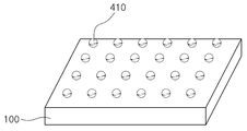
상기 패턴 홀 내에 금속 전구체를 포함하는 마이셀을 형성하는 단계; 및
상기 마이셀에 대한 산소 플라즈마 식각을 통해 금속 나노입자를 형성하는 단계를 포함하는 금속 나노입자의 형성방법. - 제5항에 있어서, 상기 고분자층은 PVA(Poly(vinyl alcohol))이고, 상기 고분자 자기조립층은 PS-b-P2VP(Polystyrene-block-Poly(2-vinylpyridine) copolymer)인 것을 특징으로 하는 금속 나노입자의 형성방법.
- 제5항에 있어서, 상기 용매-증기 어닐링은 10℃ 내지 100℃의 온도로 THF를 상기 고분자 자기조립층에 증기의 형태로 공급하여 상분리를 유도하는 것을 특징으로 하는 금속 나노입자의 형성방법.
- 제5항에 있어서, 상기 마이셀은 PS-b-P4VP(Polystyrene-block-poly(4-vinylpyridine) copolymer)에 금속 전구체가 화학적으로 결합된 것을 특징으로 하는 금속 나노입자의 형성방법.
Priority Applications (1)
| Application Number | Priority Date | Filing Date | Title |
|---|---|---|---|
| KR1020150088200A KR101830476B1 (ko) | 2015-06-22 | 2015-06-22 | 금속 나노입자의 규칙배열 형성방법 |
Applications Claiming Priority (1)
| Application Number | Priority Date | Filing Date | Title |
|---|---|---|---|
| KR1020150088200A KR101830476B1 (ko) | 2015-06-22 | 2015-06-22 | 금속 나노입자의 규칙배열 형성방법 |
Publications (2)
| Publication Number | Publication Date |
|---|---|
| KR20170000009A true KR20170000009A (ko) | 2017-01-02 |
| KR101830476B1 KR101830476B1 (ko) | 2018-02-21 |
Family
ID=57810368
Family Applications (1)
| Application Number | Title | Priority Date | Filing Date |
|---|---|---|---|
| KR1020150088200A Expired - Fee Related KR101830476B1 (ko) | 2015-06-22 | 2015-06-22 | 금속 나노입자의 규칙배열 형성방법 |
Country Status (1)
| Country | Link |
|---|---|
| KR (1) | KR101830476B1 (ko) |
Cited By (2)
| Publication number | Priority date | Publication date | Assignee | Title |
|---|---|---|---|---|
| CN110943040A (zh) * | 2018-09-21 | 2020-03-31 | 三星电子株式会社 | 切割衬底的方法和用于形成半导体芯片的分离方法 |
| KR20230143809A (ko) * | 2022-04-06 | 2023-10-13 | 한국화학연구원 | 음각의 패턴을 가지는 리튬금속전지용 집전체, 그 제조방법 및 이를 포함하는 리튬금속전지 |
Families Citing this family (1)
| Publication number | Priority date | Publication date | Assignee | Title |
|---|---|---|---|---|
| KR102963863B1 (ko) * | 2019-11-26 | 2026-05-11 | 재단법인 포항산업과학연구원 | 응축수 수집기 |
Family Cites Families (2)
| Publication number | Priority date | Publication date | Assignee | Title |
|---|---|---|---|---|
| KR101238551B1 (ko) | 2010-09-29 | 2013-03-04 | 한국과학기술원 | 나노입자 어레이 제조방법, 이에 의하여 제조된 나노입자 어레이, 플라즈몬 나노입자를 포함하는 바이오 센서의 제조방법, 이에 의하여 제조된 바이오 센서 및 이를 이용한 바이오 물질 센싱방법 |
| KR101412228B1 (ko) | 2012-06-11 | 2014-07-02 | 한국과학기술원 | 혼합 블록공중합체 박막 제조방법, 혼합 블록공중합체 주형 제조방법 및 이에 의하여 제조된 혼합 블록공중합체 박막 및 주형 |
-
2015
- 2015-06-22 KR KR1020150088200A patent/KR101830476B1/ko not_active Expired - Fee Related
Cited By (2)
| Publication number | Priority date | Publication date | Assignee | Title |
|---|---|---|---|---|
| CN110943040A (zh) * | 2018-09-21 | 2020-03-31 | 三星电子株式会社 | 切割衬底的方法和用于形成半导体芯片的分离方法 |
| KR20230143809A (ko) * | 2022-04-06 | 2023-10-13 | 한국화학연구원 | 음각의 패턴을 가지는 리튬금속전지용 집전체, 그 제조방법 및 이를 포함하는 리튬금속전지 |
Also Published As
| Publication number | Publication date |
|---|---|
| KR101830476B1 (ko) | 2018-02-21 |
Similar Documents
| Publication | Publication Date | Title |
|---|---|---|
| TWI392643B (zh) | 利用金屬氧化物使自組嵌段共聚物選擇性穿透的方法,形成金屬氧化物結構之方法及包含彼之半導體結構 | |
| US8399174B2 (en) | Method of forming fine patterns using a block copolymer | |
| TWI359458B (en) | Alternating self-assembling morphologies of dibloc | |
| CN102983065B (zh) | 图案、掩模图案形成方法和半导体器件制造方法 | |
| EP2948817B1 (en) | Surface nanofabrication methods using self-assembled polymer nanomasks | |
| JP4923904B2 (ja) | 親水性および/または親油性の異なる領域を同一表面上に備える基板を生産する方法 | |
| WO2016065308A1 (en) | Nanoshape patterning techniques that allow high-speed and low-cost fabrication of nanoshape structures | |
| KR20090083091A (ko) | 블록 공중합체를 이용한 미세 패턴 형성 방법 | |
| TW201008867A (en) | Graphoepitaxial self-assembly of arrays of downward facing half-cylinders | |
| US11923197B2 (en) | Methods of forming nanostructures utilizing self-assembled nucleic acids | |
| CN101432224A (zh) | 表面排列有微细金属块的基板 | |
| KR101830476B1 (ko) | 금속 나노입자의 규칙배열 형성방법 | |
| US12002861B2 (en) | Method of forming conductive contacts on graphene | |
| CN105278240A (zh) | 制造嵌段共聚物的方法和由其制造的物品 | |
| US20080280099A1 (en) | Silicon Substrates with Thermal Oxide Windows for Transmission Electron Microscopy | |
| CN107258009A (zh) | 用于湿法蚀刻嵌段共聚物自组装图案的方法 | |
| KR20150092397A (ko) | 블록 공중합체 및 이를 사용한 패턴 형성 방법 | |
| CN117701373A (zh) | 测序芯片及其制备方法 | |
| KR20100111525A (ko) | 나노 입자를 함유하는 나노 패턴의 제조방법 및 전자 소자 | |
| KR101989414B1 (ko) | 블록공중합체를 이용한 마이크로패턴 내부에 정렬된 금속 나노선 및 이의 제조방법 | |
| KR20150143222A (ko) | 패턴화된 실리카 입자 제조방법 및 이를 통해 제조된 패턴화된 실리카 입자 | |
| TW201920323A (zh) | 用於控制嵌段共聚物的奈米域定向之方法 | |
| JP2009081369A (ja) | ステンシルマスク製造方法 | |
| KR20220096324A (ko) | 초미세 패턴을 이용한 블록공중합체 정렬 방법 | |
| US11803120B2 (en) | Graphene-enabled block copolymer lithography transfer to arbitrary surfaces |
Legal Events
| Date | Code | Title | Description |
|---|---|---|---|
| PA0109 | Patent application |
St.27 status event code: A-0-1-A10-A12-nap-PA0109 |
|
| A201 | Request for examination | ||
| PA0201 | Request for examination |
St.27 status event code: A-1-2-D10-D11-exm-PA0201 |
|
| PG1501 | Laying open of application |
St.27 status event code: A-1-1-Q10-Q12-nap-PG1501 |
|
| D13-X000 | Search requested |
St.27 status event code: A-1-2-D10-D13-srh-X000 |
|
| D14-X000 | Search report completed |
St.27 status event code: A-1-2-D10-D14-srh-X000 |
|
| E902 | Notification of reason for refusal | ||
| PE0902 | Notice of grounds for rejection |
St.27 status event code: A-1-2-D10-D21-exm-PE0902 |
|
| E13-X000 | Pre-grant limitation requested |
St.27 status event code: A-2-3-E10-E13-lim-X000 |
|
| P11-X000 | Amendment of application requested |
St.27 status event code: A-2-2-P10-P11-nap-X000 |
|
| P13-X000 | Application amended |
St.27 status event code: A-2-2-P10-P13-nap-X000 |
|
| E701 | Decision to grant or registration of patent right | ||
| PE0701 | Decision of registration |
St.27 status event code: A-1-2-D10-D22-exm-PE0701 |
|
| GRNT | Written decision to grant | ||
| PR0701 | Registration of establishment |
St.27 status event code: A-2-4-F10-F11-exm-PR0701 |
|
| PR1002 | Payment of registration fee |
St.27 status event code: A-2-2-U10-U11-oth-PR1002 Fee payment year number: 1 |
|
| PG1601 | Publication of registration |
St.27 status event code: A-4-4-Q10-Q13-nap-PG1601 |
|
| P22-X000 | Classification modified |
St.27 status event code: A-4-4-P10-P22-nap-X000 |
|
| R18-X000 | Changes to party contact information recorded |
St.27 status event code: A-5-5-R10-R18-oth-X000 |
|
| PR1001 | Payment of annual fee |
St.27 status event code: A-4-4-U10-U11-oth-PR1001 Fee payment year number: 4 |
|
| PR1001 | Payment of annual fee |
St.27 status event code: A-4-4-U10-U11-oth-PR1001 Fee payment year number: 5 |
|
| PR1001 | Payment of annual fee |
St.27 status event code: A-4-4-U10-U11-oth-PR1001 Fee payment year number: 6 |
|
| P14-X000 | Amendment of ip right document requested |
St.27 status event code: A-5-5-P10-P14-nap-X000 |
|
| PN2301 | Change of applicant |
St.27 status event code: A-5-5-R10-R11-asn-PN2301 |
|
| P16-X000 | Ip right document amended |
St.27 status event code: A-5-5-P10-P16-nap-X000 |
|
| PN2301 | Change of applicant |
St.27 status event code: A-5-5-R10-R14-asn-PN2301 |
|
| PR1001 | Payment of annual fee |
St.27 status event code: A-4-4-U10-U11-oth-PR1001 Fee payment year number: 7 |
|
| R18-X000 | Changes to party contact information recorded |
St.27 status event code: A-5-5-R10-R18-oth-X000 |
|
| R18-X000 | Changes to party contact information recorded |
St.27 status event code: A-5-5-R10-R18-oth-X000 |
|
| PC1903 | Unpaid annual fee |
St.27 status event code: A-4-4-U10-U13-oth-PC1903 Not in force date: 20250213 Payment event data comment text: Termination Category : DEFAULT_OF_REGISTRATION_FEE |
|
| H13 | Ip right lapsed |
Free format text: ST27 STATUS EVENT CODE: N-4-6-H10-H13-OTH-PC1903 (AS PROVIDED BY THE NATIONAL OFFICE); TERMINATION CATEGORY : DEFAULT_OF_REGISTRATION_FEE Effective date: 20250213 |
|
| PC1903 | Unpaid annual fee |
St.27 status event code: N-4-6-H10-H13-oth-PC1903 Ip right cessation event data comment text: Termination Category : DEFAULT_OF_REGISTRATION_FEE Not in force date: 20250213 |
|
| R18 | Changes to party contact information recorded |
Free format text: ST27 STATUS EVENT CODE: A-5-5-R10-R18-OTH-X000 (AS PROVIDED BY THE NATIONAL OFFICE) |
|
| R18-X000 | Changes to party contact information recorded |
St.27 status event code: A-5-5-R10-R18-oth-X000 |